EP0169576B1 - Method and system of circuit pattern understanding and layout - Google Patents
Method and system of circuit pattern understanding and layout Download PDFInfo
- Publication number
- EP0169576B1 EP0169576B1 EP85109414A EP85109414A EP0169576B1 EP 0169576 B1 EP0169576 B1 EP 0169576B1 EP 85109414 A EP85109414 A EP 85109414A EP 85109414 A EP85109414 A EP 85109414A EP 0169576 B1 EP0169576 B1 EP 0169576B1
- Authority
- EP
- European Patent Office
- Prior art keywords
- layout
- shape
- program
- circuit
- patterns
- Prior art date
- Legal status (The legal status is an assumption and is not a legal conclusion. Google has not performed a legal analysis and makes no representation as to the accuracy of the status listed.)
- Expired - Lifetime
Links
Images


Classifications
-
- G—PHYSICS
- G06—COMPUTING; CALCULATING OR COUNTING
- G06F—ELECTRIC DIGITAL DATA PROCESSING
- G06F30/00—Computer-aided design [CAD]
- G06F30/30—Circuit design
- G06F30/39—Circuit design at the physical level
- G06F30/398—Design verification or optimisation, e.g. using design rule check [DRC], layout versus schematics [LVS] or finite element methods [FEM]
-
- G—PHYSICS
- G06—COMPUTING; CALCULATING OR COUNTING
- G06F—ELECTRIC DIGITAL DATA PROCESSING
- G06F30/00—Computer-aided design [CAD]
- G06F30/30—Circuit design
- G06F30/39—Circuit design at the physical level
-
- Y—GENERAL TAGGING OF NEW TECHNOLOGICAL DEVELOPMENTS; GENERAL TAGGING OF CROSS-SECTIONAL TECHNOLOGIES SPANNING OVER SEVERAL SECTIONS OF THE IPC; TECHNICAL SUBJECTS COVERED BY FORMER USPC CROSS-REFERENCE ART COLLECTIONS [XRACs] AND DIGESTS
- Y10—TECHNICAL SUBJECTS COVERED BY FORMER USPC
- Y10S—TECHNICAL SUBJECTS COVERED BY FORMER USPC CROSS-REFERENCE ART COLLECTIONS [XRACs] AND DIGESTS
- Y10S706/00—Data processing: artificial intelligence
- Y10S706/902—Application using ai with detail of the ai system
- Y10S706/919—Designing, planning, programming, CAD, CASE
- Y10S706/921—Layout, e.g. circuit, construction
Description
- The present invention relates to a CAD (Computer-Aided Design) system for designing circuits, such as electronic circuits, and an automatic integrated circuit layout producing system, and more particularly to a method and system for understanding a circuit pattern and laying out circuit elements, employing a knowledge data base.
- Function to understand a higher-level structure represented by nets on the basis of the basic net list information of a circuit has not been achieved by the conventional electronic circuit CAD. Accordingly, in laying out a differential amplifier in the layout of a bipolar linear circuit, for instance, it is simple for human to decide a layout conforming to the layout rule for the two component pair transistors (for example, a rule requiring the contiguous and opposite disposition of two pair transistors), whereas it is very difficult for a computer to decide the same. Prior art relating to such a function is described in detail in Jiry Soukup, "Circuit Lay-out", Proc. IEEE, vol. 169, No. 10, Oct. 1981.
- If subcircuits to be recognized need to be defined directly by the elements, variations of the subcircuits with a slight difference must be defined directly and individually, which requires an enormous storage capacity and is difficult to apply to practical circuits of wide variation.
- Furthermore, in a conventional automated electronic circuit layout method, the layout of an electronic circuit to be laid out is produced by selecting a layout shape corresponding to the elements of the electronic circuit among a shape data base storing layout shapes of circuit elements. Accordingly, it is impossible to use the layout shape data of the data base, when information for selecting the shape information among those of the shape data base is not given previously. Therefore, in determining the layout of a differential amplifier, which is often employed in an analog circuit, for instance, a layout meeting a restrictive layout condition that the two pair transistors of the differential amplifier are to be disposed contiguously and oppositely can be determined only when a condition that the differential amplifier shown in a circuit diagram comprises two pair transistors is designated in the circuit diagram and the layout shape of the differential amplifier is provided in the shape data base.
- When a layout is produced by a layout designer with reference to a circuit diagram, the layout designer understands the circuit to be a differential amplifier from the net list information of the transistors shown in the circuit diagram, even if the differential amplifier is not particularly indicated, and then the layout designer is able to produce an appropriate layout on the basis of his knowledge of the layout restrictions as to differential amplifiers. The layout shape of the differential amplifier can also be determined from the electrical characteristics of the differential amplifier.
- It is desirable to provide a computer with the functions of the layout designer in order to improve the functions of a layout producing system.
- Still further, a standard cell system (Saburo Muroga, "VLSI System Design", Wiley Interscience, 1982) has been a well-known automatic layout method for laying out a digital electronic circuit. According to this method, a plurality of the combinations of predetermined elements (transistor and resistance, a plurality of transistors, those elements of different constants) are provided in fixed shapes in a library as standard cells, and the combinations coinciding with the elements of the desired circuit to be laid out are selected and connected.
- Recently, the necessity of analog-digital compounded LSIs has increased with the expansion of demand for LSIs, and the curtailment of design work load, particularly, that of the work load on layout designers, is a significant object. In order to achieve such object, an automatic layout system for laying out analog circuits has been desired. However, differing from automated process for laying out a digital circuit, automated process for laying out an analog circuit is required to change the layout shape of circuit elements and parts so as to meet the characteristics of the elements and parts or the shape of the variable area for layout. Accordingly, the conventional standard cell system applicable to the digital system, in which the shapes of cells are fixed, is not applicable to laying out an analog circuit without modification.
- Furthermore, in a conventional automatic layout system for laying out electronic circuits of the digital system, elements of known shapes to be laid out are arranged in a manner to reduce the wiring distance between the elements and the elements are interconnected by automatic wiring. When an increased number of elements need to be laid out, even a computer is unable to provide a satisfactory plan of layout, as there are numerous alternative modes of layout.
- In a logic language, such as Prolog, of knowledge information system for processing such a layout, one of the artificial intelligence techniques employs a system in which various conceptions are stored and retrieved in a mode of conception, "the property O of A is V", for example, as described in P. H. Winston, B. K. P. Horn; "LISP", Chapt. 22, Addison-Wesley Publishing Co., 1981 and others. In case the layout shape of transistors is stored in laying out a circuit, when information, "The size of the shape of the base diffusion layer of trl is 4 x 5" is provided, [4, 5] can be stored with A = tr1, O = base diffusion and V = shape.
- On the contrary, when A and O are given, the value of V can be retrieved. In the above-mentioned example, an answer [4, 5] is given to a question, "What is the shape of the base diffusion of tri?"
- Thus, the retrieval system employing a form of conception represented by A, O and V uses only a simple retrieval keyword expression and a natural language, and hence this retrieval system is capable of storing and retrieving extremely numerous conceptions.
- Such a useful A-Q-V retrieval system will often be employed in information processing techniques for CAD.
- A logic program such as artificial intelligence language Prolog, which has recently become a topic of the related arts, includes a back tracking mechanism and is capable of automatically retrieving an effective plan among various possible alternative plans. Accordingly, this logic program is deemed to occupy an important position in the future CAD techniques.
- However, the logic program, in general, does not allow the use of global variables, namely, the common variables in FORTRAN, and hence it is usual to change the program described by the language while the program is executed, to achieve the A-Q-V retrieval system on the logic program, which adversely affects the processing efficiency.
- A CAD system for the automatic layout of electronic circuits according to the first part of
claim 1 is known from IEEE Transactions on Circuits and Systems, vol. CAS-30, no. 6, June 1983, pages 358-364. The known system is a hierarchical layout system wherein sub-blocks are chosen to match as nearly as possible a desired shape and size, by appropriate placing and routing within the sub-blocks, and at the lowest level by a choice of layout implementations of fundamental cells. - It is an object of the present invention to provide a system and a method for the automatic layout of electronic circuits, capable of coping with variations often appearing in actual circuits by recognizing, understanding and extracting a significant higher-level structure (sub-circuit) from net-list information concerning the elementary elements of such circuits.
- This object is met by the system of
claim 1 and the method ofclaim 2, preferred embodiments of the invention being set forth in the dependent claims. -
- Fig. 1 is a block diagram showing the functional constitution of an electronic circuit structure understanding system according to the present invention;
- Fig. 2 is a diagram of a conventional circuit, provided for information in explaining the embodiments of the present invention;
- Fig. 3 is an explanatory diagram of basic net list information of the circuit of Fig. 2, for assistance in explaining the present invention;
- Fig. 4 is an explanatory diagram for assistance in explaining an embodiment of a structural pattern according to the present invention;
- Fig. 5 is a diagram showing instructions for executing a circuit structure understanding program according to the present invention and the resultant outputs;
- Fig. 6 is a conceptional illustration showing the general constitution of a second embodiment of the present invention;
- Fig. 7 is a block diagram showing the operational environment of the present invention;
- Fig. 8 is an explanatory illustration of an embodiment of the present invention;
- Fig. 9 is a view showing the source listings of operations for recognition and extraction according to the present invention;
- Figs. 10(a) and 10(b) are explanatory illustrations of an embodiment of the present invention;
- Fig. 11 is an explanatory illustration showing the definition of blocks of a third embodiment of the present invention;
- Fig. 12 is a block diagram showing an example of a hardware environment for carrying out the present invention;
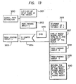
- Fig. 13 is a PAD (Problem Analysis Diagram) flow chart of the signal propagation line extraction procedure of the third embodiment of the present invention;
- Fig. 14 is a circuit diagram showing the results of exemplary signal propagation path extraction performed according to the present invention;
- Figs. 15(a) and 15(b) are block diagrams showing the organisation of a system, in a fourth embodiment, according to the present invention;
- Fig. 16 is a flow chart showing the processes of the fourth embodiment of the present invention;
- Fig. 17 is a circuit diagram of an exemplary electronic circuit to be processed by the embodiment in relation to the prior art;
- Fig. 18 is a circuit layout showing the layout shape of the parts of a circuit;
- Fig. 19 is an explanatory illustration showing a mode of layout according to the present invention;
- Fig. 20 is a conceptional illustration for the explanation of the hierarchical structure of an objective electronic circuit of a fifth embodiment of the present invention;
- Fig. 21 (a) is a block diagram of the hardware environment of an embodiment of the present invention;
- Fig. 21 (b) is an illustration showing the functional structure of a software of the system according to the present invention;
- Fig. 22 is a flow chart showing the steps of processes of the system according to the present invention;
- Figs. 23 and 24 are conceptional illustrations of layout patterns according to the present invention;
- Fig. 25 is an explanatory illustration showing the results of layout obtained by the method according to the present invention;
- Fig. 26 is a block diagram showing the functions of an automatic production system for producing electronic circuit layout, in a sixth embodiment, according to the present invention;
- Fig. 27 is a flow chart showing the processes of the program of the system of Fig. 26;
- Fig. 28 is an explanatory illustration of an example employing a resistance layout shape as a cell shape;
- Fig. 29 is an LSI layout on a substrate formed according to the present invention;
- Figs. 30(a) and 30(b) are explanatory illustrations of a cell combination according to the present invention;
- Fig. 31 is an explanatory illustration of an input program and an output program each according to the present invention;
- Figs. 32 and 33 are explanatory illustrations of programs for producing a cell layout shape plan according to the present invention;
- Fig. 34 is an explanatory illustration of a cell layout plan selecting program according to the present invention;
- Fig. 35 is an explanatory illustration of the component functions of an AOV retrieval system, in a seventh embodiment, according to the present invention; and
- Fig. 36 is a block diagram showing a hardware environment for executing the seventh embodiment of the present invention.
- A first embodiment of the present invention will be described hereinafter in connection with the accompanying drawings including Fig. 1.
- Fig. 1 shows the constitution of a system embodying the present invention. In Fig. 1, indicated at 100 is an electronic circuit structure understanding system, at 110 is an inference mechanism, at 120 is a knowlege base internally containing a
structure pattern 122 and an electronic circuit elementarynet data 124, and at 130 is a terminal equipment. - This embodiment will be described on an assumption that the present invention is embodied in the Prolog language for artificial intelligence. The Prolog language is advantageous since the
inference mechanism 110 can be realized by the inherent inference mechanism of the Prolog language. The Prolog language and the inference mechanism thereof are described in detail in "Clocksin and Mellish 81; Programming in Prolog, Springer-Verlag, 1981", and hence the description thereof will be omitted. - Fig. 2 shows a concreter example of an electronic circuit. In Fig. 2, indicated at 200 is a differential amplifier, and at 211, 212 and 213 are npn transistors. An electronic circuit structure understanding system will be described hereunder with reference to this circuit shown in Fig. 2.
- Fig. 3 shows an example of the expression of the basic net list information of the electronic circuit of Fig. 2 in the Prolog language. This expression corresponds to the contents of the electronic circuit elementary
net data 124 of Fig. 1. - In Fig. 3, a
reference numeral 300 indicates the existence of an npn transistor designated at tr1 and the base, the collector and the emitter are connected to nodes n1' nµ and n10 respectively. Fig. 3 also gives descriptions similar to that for the npn transistor tr1 for two other transistors. - In Fig. 3, a
reference numeral 302 indicates the existence of a resistance r1 and the nodes thereof are n3 and ng. Similar descriptions are given for two other resistances. - In Fig. 3, a
reference numeral 304 indicates that nodes n8 and n4 are interconnected. Similar descriptions are given for other connections. - In Fig. 3, a
reference numeral 308 indicates that a node n4 is an output node. A similar description is given for a node ns. - In Fig. 3, a
reference numeral 310 indicates that a node n3 is Vcc and areference numeral 312 indicates that a node n7 is VEE. - Fig. 4 is a structural pattern for understanding the structure of the
differential amplifier 200 of the circuit diagram shown in Fig. 2 and this structural pattern is an example of the contents of thestructural pattern 122 of Fig. 1. When a structure other than the differential amplifier needs to be understood, then like the differential amplifier which will be described hereunder, a pattern for structure understanding is produced and the same is provided in thestructural pattern 122 of the knowledge base of Fig. 1. - In Fig. 4, a
reference numeral 400 indicates that a structure having four variables, i.e., TR1, TR2, R1 and R2 (capitalized words are variables, while those consisting of small letters are constants), is a differential amplifier. TR1 and TR2 are variables to which actual transistor designations are assigned after structural understanding, while R1 and R2 are variables to which resistance designations are assigned. This example is a pattern for understanding a differential amplifier consisting of two transistors and two resistances. In a part indicated by 400, a mark ":-" separates the right-hand side and the left-hand side; the "COMPARATOR (TR1, TR2, R1, R2)" is the left-hand side and 402 to 410 are the right-hand side. The left-hand side is the object of structural understanding (a differential amplifier in this example) and the right-hand side represents preconditions for the left-hand side to be true. - A
reference numeral 402 indicates that a differential amplifier needs to have two transistors. The transistors are designated by variables TR1 and TR2, which are the same as the variables TR1 and TR2 of the left-hand side. Areference numeral 404 indicates that the actual designations of the two transistors of 402 indicated by the designations TR1 and TR2 need to be different. Areference numeral 406 indicates that the emitters of the two transistors need to be connected to one and the same node (EM1 == EM2) and that the respective types of the two transistors need to be the same (TYPE 1 == TYPE 2). - A
reference character 408 indicates that two resistances need to be provided. - A
reference numeral 410 indicates that the nodes of the two resistances need to meet one of the four conditions (";" is a logical OR symbol). The first condition indicates that a real node indicated by the node variable N11 of one of the resistance and a real node indicated by the node variable N21 of the other resistance are the same, a real node indicated by a resistance node variable N12 and a real node indicated by the collector node variable COL1 of the transistor tr1 are the same, and a real node indicated by the collector node variable COL2 of the transistor tr2 and a real node indicated by the node variable N22 of the resistance are the same. Three other definitions shown in Fig. 4 are the same as the above-mentioned definition, therefore, the description thereof will be omitted. - Fig. 5 shows a manner of giving instructions from the terminal of Fig. 1 for the structural understanding of a differential amplifier. A
reference numeral 500 indicates an instruction, "Understand the structure of a differential amplifier having variables X, Y and Z" described in the Prolog language. When this instruction is given, theinference mechanism 110 of Fig. 1 accesses information shown in Fig. 4 among the information included in the knowledge base, then finds a condition that meets the first condition tr (TR1,TYPE 1,BASE 1,COL 1, EM1) of the right-hand side from the basic net list information of the electronic circuit shown in Fig. 3, and then assigns the information to be matched to the variables TR1,TYPE 1,BASE 1,COL 1 and EM1. In this example, the first one among theconditions 300 of Fig. 3 matches the first condition tr of the right-hand side and tr1, npn, n1, n9 and n10 are assigned to the variables respectively. Details of this procedure are described in the abovementioned literature "Clocksin and Mellish 81", and hence the detailed description thereof will be omitted. Thereafter, other conditions of the right-hand side are subjected to matching with the contents of Fig. 3 sequentially while the variables once assigned to constants are fixed to decide the values of the variables meeting all the conditions of the right-hand side. In case of failure, another matching object that meets the prior condition is searched for automatically. Finally, as indicated at 510 in Fig. 5, a conclusive output indicating that the differential amplifier consisting of two transistors tr1 and tr2, and two resistances r1 and r2 is found in the basic net list information of the electronic circuit of Fig. 3 is displayed. That is, the existence of the differential amplifier is understood by the computer. - Structural understanding of various electronic circuits can be achieved by changing the contents of the
condition 124, while the contents of thestructural pattern 122 of Fig. 1 are fixed. - The present invention has been described with reference to a differential amplifier, however, the present invention is capable of understanding other structural patterns on the basis of the above- mentioned spirit, provided that net patterns specific to electronic circuits (structural patterns) or high-level structures are stored previously in the knowledge base.
- According to the present invention, the basic net list information of an electronic circuit as shown in Fig. 3 is given to make a computer achieve the understanding of upper level semantics.
- Application of the present invention to an electronic circuit layout CAD system enables a computer to execute an operation, "Place the two pair transistors of a differential amplifier adjacently and symmetrically", which is possible when a human produces a layout with reference to Fig. 2, when the basic net list information of electronic circuits is given, and thereby a layout of a higher grade as compared with conventional layout can be produced.
- Although there are various net patterns or rules specific to electronic circuits, other layouts of electronic circuits can be determined in the same manner as described hereinbefore.
- A second embodiment of the present invention will be described hereinafter.
- Fig. 6 shows a system employing a computer, embodying the present invention. A circuit
net data 1 is given to thecomputer 2 as an input. Thecomputer 2 collates the input with internally storedsubcircuit definitions 3 and provides asubcircuit 4 meeting the definition. The present invention is characterized by the recursive matching of the input with thedefinitions 3 for flexible matching. - Fig. 7 shows an exemplary hardware environment for carrying out the operations of the present invention. An input pattern given to a CPU by means of a keyboard entry unit and a pattern input tablet is matched with the
definitions 3 by the CPU, and then the CPU gives an output to a draftingmachine 18 or the like. Pattern files are stored also in adisk unit 13 or the like, and hence it is possible to provide an output on a printer or a display unit. - Fig. 8 shows the recursive definition of a subcircuit, i.e., a voltage dividing resistor. The
voltage dividing resistor 2100 is defined as a circuit having a serial connection ofresistances anode terminal 2104, acathode terminal 2105 and a voltage dividing terminal 2106, or as a circuit having a serial connection of aresistance 2107 and avoltage dividing resistor 2103, ananode terminal 2104, acathode terminal 2105 and avoltage dividing terminal 2106. In this embodiment, since recursive definition is made, a voltage dividing resistor can be recognized and extracted regardless of the number of the resistances. A source list for the recursive definition of the voltage dividing resistor for the actual extraction of the voltage dividing resistor in the Prolog language is shown in Fig. 9. (Refer to "Clocksin and Mellish (translation by Nakamura)" Prolog Programming, Japan Computer Assoc., for the Prolog language). - Fig. 10 shows a definition of a logical operation circuit having an optional combination of an NAND logic and a NOR logic (designated as "serial-parallel inverter") by the use of a serial-parallel pulldown, a recursively defined nonterminal symbol. The serial-
parallel inverter 2200 has a depletion-mode MOSFET 2201 connecting apower source 2202 to a serial-parallel pulldown 2203 connected toearth 2204, aninput terminals 2205 and anoutput terminal 2206 as shown in Fig. 10(a). A serial-parallel pulldown 2203 is a circuit having an enhancement-mode MOSFET 2216, ananode terminal 2210, aninput terminal 2209 and acathode terminal 2211, or a circuit having a serial connection of serial-parallel pulldowns anode terminal 2210,input terminals 2209 and acathode terminal 2211, or a circuit having a parallel connection of serial-parallel pulldowns anode terminal 2210,input terminals 2209 and acathode terminal 2211, as shown in Fig. 10(b). Since this embodiment is recursively defined, this embodiment is able to recognize and extract a NMOS inverter of a variety of forms. - Thus the second embodiment of the present invention is capable of recognizing and extracting a sub- circuit corresponding to a variety of circuits.
- A third embodiment of the present invention will be described hereinafter with reference to Figs. 11 to 14. The object of this embodiment is a subcircuit of high input impedance and low output impedance which can be incorporated into a circuit network as it is without deteriorating the characteristics thereof.
- Fig. 11 also shows defining a
block 3100 by the use of apull 3103 and apush 3104, namely, recursively defined nonterminal symbols. Theblock 3100 has aninput node 3101 and an array ofoutput nodes 3102 and is defined, as shown in Fig. 11, by pulls 3103,transistors push 3104. Indicated at 3107 is an output terminal of the circuit. Thepull 3103 is defined as a circuit having aresistance 3112,transistors condenser 3113, ananode node 3109, acathode node 3110 andoutput nodes 3108, or a circuit having a serial connection of pulls. The push is defined as a circuit having thetransistors input node 3114 and anoutput node 3111, or a circuit having a serial connection of pushes. The various definitions of these blocks are stored in a memory and the relation between the net and the blocks are defined beforehand. Fig. 12 shows a hardware environment for carrying out the present invention. The above-mentioned definitions are stored in amemory 3924 and amagnetic disk memory 3925. A circuit to be extracted is entered into aCPU 3921 by means of akeyboard entry unit 3923 or atablet 3922. The output of theCPU 3921 is given to adisplay unit 3926, adrafting machine 3927 or aprinter 3923, according as occasion demands. - The block defined as shown in Fig. 11 has a single input node and multiple output nodes. Therefore, repetition of a procedure comprising selecting an input node of the circuit as an input node, retrieving the block and retrieving another block by employing one of the obtained output nodes as an input node, until extraction becomes impossible achieves the search for the signal propagation path of the circuit. A PAD diagram (flow chart) of the procedure for extracting a signal propagation path from such a circuit through the depth first search of the block is shown in Fig. 13. (Refer to "Application of PAD (Problem Analysis Diagram) to the Design and Production of Programs"; Mimura et al., for PAD). Signal
propagation path extraction 3200 is a path search (3202) about L by substituting the list of input nodes of a circuit for L (3201). Path search about L (3203) is ended (3205) if L is an empty list (3204). If not (3204), the first element of L is held as Head and the rest of the elements of L are defined as Tail (3206), a block whose input node is Head is extracted, the output nodes of the block are defined as Outputs (3207), recursive path search is carried out about the Outputs (3208), recursive path search is carried out about the Tail (3209), and the block extracted atStep 3207, the block list extracted atStep 3208 and the block list extracted atStep 3209 are put together into a single block list and returned. - Thus the present invention uses blocks of the same kind for defining a block and the same path searching procedure as used for the preceding path searching is employing in the succeeding path search for the rest of the paths, and hence the path search of the present invention is recursive.
- The result of application of the present invention to an actual circuit is shown in Fig. 14. A
signal propagation path 3301 was recognized and extracted by extracting ablock 3302 having aninput terminal block 3303 employing the output node of theblock 3302 as an input node, and extractingblocks - The embodiment has been described as applied to a computer software, however, the algorithm of the present invention can partially be carried out by a microcomputer or a special purpose hardware, or can be realized by a device.
- The third embodiment of the present invention is capable of extracting a signal propagation path from the net list information of the circuit alone.
- A fourth embodiment of the present invention will be described hereinafter with reference to Figs. 15 to 19.
- Fig. 15(a) shows a hardware environment for carrying out the present invention. Net data is entered by means of a
keyboard 42, alight pen 43 and atablet 44. A knowledge base and a data base are stored in amemory 46 and amagnetic disk file 45. The result of layout and interim results are provided by output units, namely, adisplay 47, a draftingmachine 48 and aprinter 49. - Fig. 15(b) shows a software system according to the present invention. In Fig. 15(b), indicated at 4100 is a computer. In this embodiment, i.e., the layout system, the input data is circuit elementary
net data 4110, while the output data iscircuit layout data 4120. - This system includes a circuit structure understanding function and a circuit layout function, which are realized by a program for
circuit structure understanding 4140 and acircuit layout program 4160 respectively. - The program for
circuit structure understanding 4140 understands and extracts a characteristic partial structure of a circuit included in the circuit elementarynet data 4110 by using knowledge forcircuit structure understanding 4130, and produces circuitintermediate structure data 4150. - The
circuit layout program 4160 converts the circuitintermediate structure data 4150 intocircuit layout data 4120 by using acircuit layout library 4170 storing the layout shape producing knowledge for the partial structure of the circuit. - Fig. 16 shows the steps of processes of this system.
- As mentioned above, at the
first step 4200, circuit structure understanding is executed. At this step, the circuitnet data 4110 is converted into the circuitintermediate structure data 4150 by using the knowledge forcircuit structure understanding 4130. - At the
next step 4210, circuit layout is executed. At this step, the circuitintermediate structure data 4150 is converted into thecircuit layout data 4120 by using thecircuit layout library 4170. - Fig. 17 shows a circuit with which this embodiment deals. In Fig. 17, indicated at 4300 is a differential amplifier, at 4301,4302 and 4303 are resistances, at 4311,4312 and 4313 are npn transistors and 4321,4322 and 4323 are nodes.
- When a person considers the layout of the circuit, the person understands that a
configuration 4300 of Fig. 17 is a differential amplifier and places the twopair transistors - In the following description of the embodiment, the artificial intelligence language Prolog is employed. Refer to, for example, "Clocksin and Mellish; Programming in Prolog, Springer-Verlag, 1981" for this language.
- In
Program List 1, the circuit elementarynet data 4110 of Fig. 15 is described in the Prolog language and the circuit elementary net data corresponds to the circuit shown in Fig. 17, except the step 460. - In
Program List 1,step 400 indicates that a transistor trl are connected to nodes n1, n9 and n20 respectively, and the allowable current is 1. - Step 410 indicates that a resistor r1 has nodes n3 and ng, and the resistance is 10. Step 420 indicates that nodes n8 and n4 are interconnected. Step 430 indicates that the node n, is an input terminal, while step 450 indicates that the node n3 is a Vcc terminal.
- Step 460 is not included in the circuit elementary net data, and is the result of circuit structure understanding by using the circuit elementary net data. The program including step 460 corresponds to the circuit
intermediate structure data 4150 of Fig. 16. Step 460 indicates that a differential amplifier designated asComp 1 is included, two npn transistors tr1 and tr2 are included, maximum current is 1, resistors r, and r2 are included, and the respective values of resistance of the resistors r1 and r2 are 10 and 20.
-
Program List 2 indicates the exemplary contents of the knowledge forcircuit structure understanding 4130 of Fig. 15. In this program list,step 500 and the following steps represent knowledge for understanding the differential amplifier.Steps 510 and 520 indicate that two transistors need to be included. Steps 530 and 540 indicate that two transistors need to be different from each other and the respective emitters of the transistors need to be connected to a common node. Steps 550 and 560 indicate that two resistances need to be included. Step 570 indicates that the two resistances need to be connected to the collectors of the transistors. Step 580 indicates an instruction to query an external unit for the designation of the differential amplifier which has been understood.
-
Program List 3 corresponds to the program forcircuit structure understanding 4140 of Fig. 15. Step 600 is the head of the program for circuit structure understanding. Step 610 is a step for setting an object of structure understanding. When the contents of information are those as described in step 660, the first variable X is a comparator and first the structure understanding of a differential amplifer is executed. Step 620 indicates the production of data structure Z for circuit structure understanding. The substance of step 620 is shown at step 650. Step 630 indicates circuit structure understanding from the elementary net data of the program list by using the data structure Z produced at step 620 and the contents of the knowledge base for structure understanding ofProgram List 2. Step 640 indicates the addition of the understood structure to the data ofProgram List 1. Step 460 shows the results of step 640. - Step 670 indicates an external instruction provided for calling the program of step 600. Step 680 indicates an output provided when step 580 of
Program List 2 is executed during the execution of step 630. Step 690 indicates an externally given designation of the differential amplifier after structure understanding. Step 695 is an output provided as a result of understanding at step 640. This result indicates that the existence of a differential amplifier in the elementary net data ofProgram List 1 has been understood.
- Fig. 18 shows a layout shape of a circuit components for assistance in explaining the layout function of this embodiment.
- In Fig. 18, there are shown a
resistor 4720 to be formed in the diffusion layer formed over a wafer, aresistor shape 4722 over the diffusion layer and acontact hole 4724 extending between the diffusion layer and the outside. The resistor shape is defined by X, Y, W1, W2, W3 and E shown in Fig. 18. - There are also shown a
layout shape 4740 of an npn transistor, anisolation region 4742, acollector region 4744, acollector contact hole 4746, abase diffusion region 4748, abase contact hole 4750, anemitter region 4752, and anemitter contact hole 4754. The shape of the npn transistor is defined by X, Y and W1 to W7. - Indicated at 4780 is a layout shape of a differential amplifier. Indicated at 4782 and 4784 are the external shapes of resistors and indicated at 4786 and 4788 are the external shapes of two paired transistors. Indicated at 4790 is aluminum wiring. The layout shape of the differential amplifier is defined by X, Y and W1 to W20 as shown in Fig. 18. As well-known, these layout shapes are dependent on the electrical characteristics of the resistors, transistors and differential amplifiers respectively.
-
Program List 4 shows the concrete contents of thecircuit layout library 4170 of Fig. 15. - Step 800 indicates a program for resistor layout to give the shape of the
resistor 4720 of Fig. 18 to ANS. Step 810 is a program to read the resistance OHM of the relevant resistor from the program list data and step 820 is a program to give the resistor shape of the given resistance OHM to ANS. Step 830 is the realization of step 820. Step 840 is a program to read the size W1 of the contact hole of the resistor, in which the data given in step 850 causes W1 to be 5. Step 860 indicates that the width of the diffusion layer of the resistance is 10. Step 870 indicates that the resistance value per unit length of the resistance of 10 width is 2.


- Step 880 is a program to layout a transistor of a name, TRNAME, and to return the result to ANS, and its constitution is quite similar to that for the resistor. Step 890 and the following steps indicate that the shape of the transistor is dependent on maximum current.
- Step 890 indicates that the width of the
isolation region 4724 of thelayout shape 4740 shown in Fig. 18 is 10 when the maximum current is 10 or below and the same is 20 when the maximum current is over 10. - Step 892 is a program for laying out a differential amplifier. The constitution of this program is similar to that for the resistor.
-
Program List 5 provides thecircuit layout program 4160 of Fig. 15. - Step 900 is the head of the layout program. Step 902 is a program for the initial data setting process to produce a layout region. Step 904 is a program of a process for setting factors to be laid out. First a differential amplifier is laid out from the data given in step 924. Step 906 defines the data or the structure of the object to be laid out. Step 926 shows the realization of step 906. Step 908 indicates the execution of the layout.


- Step 910 is a program for assuming the position of a laid-out object on a two-dimensional plane with coordinates (I, J) is a candidate place. Step 930 is a concrete program for producing a candidate place. Step 912 is a program for assuming the direction of the object laid-out at the candidate place. As shown in step 932, the direction may be selected among four directions, 0°, 90°, 180° and 270°.
- Step 914 is a program for determining a vector (ZX, ZY) obtained by turning a two-dimensional vector (DX, DY) through an angle R. Step 934 shows the realization of step 914.
- Step 916 is a program for making a decision as to whether or not a rectangle of 11 width and J1 length can be placed at the candidate place (I, J). Step 936 shows the realization of step 916. As shown at step 938, a decision as to whether or not any object has already been laid out is made at step 937.
- Step 918 is a program for storing the layout shape of the object to be laid out in ZZ. Step 920 is a program for storing a region in which further layout of any object is impossible due to the layout of the object stored in ZZ. Step 922 is a program for giving the contents of ZZ to an external unit and displayng the same.
- Step 928 indicates a region for laying out an object; the region is a plane of 500 width and 500 length.
- Step 940 shows a function for checking whether or not any objects overlap.
- Step 942 is an external input to operate the layout program 900, and the resultant output is given to an external unit at step 922. Steps 944 and 946 indicate the outputs of step 922. The contents of the
circuit layout data 4120 of Fig. 15 are the same as the contents of steps 928, 938 and 946, and hence the description of the contents of thecircuit layout data 4120 will be omitted. - Step 946 indicates that a differential amplifier, compl, is laid at a position (101, 1) at an angle of 0°.
- Fig. 19 shows a layout region 928, laid-out objects 938 and differential amplifier layout 946.
- As apparent from Fig. 19, a
differential amplifier 4920 is placed by avoiding an obstacle, i.e.,box 4910 on aplane 4900 of (500, 500). In thedifferential amplifier 4920, pairedtransistors resistors - It is apparent from what has been described hereinbefore that the differential amplifier of the electronic circuit shown in Fig. 17 can correctly be laid out as shown in Fig. 19 through the procedures of Fig. 16 by the layout system with the functional organisation of Fig. 15.
- The circuit data used for this layout was that in
steps 400 to 460 excluding step 460 ofProgram List 1. That is, only the elementary circuit data was used. Nevertheless, the existence of a differential amplifier was understood by employing knowledge for circuit structure understanding, and the correct layer of the differential amplifier was decided by using knowledge of differential amplifier layout on the basis of the result of understanding. - Although the present invention has been described hereinbefore with reference to the embodiments thereof as realized by software, the algorithm of the present invention may be realized by means of hardware, namely, may partially be realized by means of a microcomputer or may be realized by special purpose hardware.
- The present invention is capable of realizing a highly intelligent layout system capable, for example, of understanding the existence of a differential amplifier in a circuit and achieving correct layout of the components according to the result of understanding only from the given elementary net data of the circuit. Such functions have not been realized by the conventinal layout CAD system and have been possible only by a person. Thus the present invention is capable of providing an automatic layout CAD system.
- The fifth embodiment of this invention will be described using Fig. 20 which illustrates the layout object conceptually. Reference number (5100) denotes a layout object (block) with a name of 'do' and an expected area of 750. The block 'do' includes three sub blocks do1 (5110), do2 (5120) and do3 (5130) with connections existing between the sub blocks. There are five connections do1 and do2, and there are three between do2 and do3.
- Block do1 (5140) has an individual hierarchical structure with an estimated area of 450 for example, and includes a block do11 (5142) and other blocks with connections existing between the blocks.
- Block do11 (5150) has an estimated area of 150, and includes blocks do5111, do5112 and do5113.
- Block do5111 (5160) is made up of elementary blocks b15 (5162), B16 (5164) and so on, and the block B15 (5170) is an elementary circuit with a fixed size of 4 by 6 as shown in the figure.
- The following describes the method of layout for the circuit which is described in a hierarchical structure as shown in Fig. 20. For clarifying the explanation, only the layout function of this embodiment will be described and the wiring function will be omitted.
- Fig. 21 (a) shows the hardware environment for carrying out this invention. Net data is entered through the
keyboard 5912,light pen 5913 andtablet 5912. The knowledge base and data base are realized by thememory unit 5916 and magneticdisk file unit 5915. The layout result and intermediate result are output on thedisplay unit 5917,plotter 5918 andprinter 5919. - Fig. 21 (b) shows the software organization of this invention. The
computer system 5200 is connected with the data file 5120 for the hierarchical system shown in Fig. 20, the hierarchicallayout program file 5220,pattern library file 5230 and output data file to which the layout result is delivered. - Fig. 22 shows the layout process in a flowchart.
- Initially, a layout block name (usually the highest-level block name, such as 'do' in Fig. 20) and a layout target shape of the block measured on the absolute coordinates are given (step 5300). Next, the estimated area, sub block name and other information about the block are examined (step 5304). Next, the initial layout candidate of the block is memorized (step 5302) so that it is used in selecting a satisfactory layout candidate in the later process. Next, one of the pattern libraries is selected (step 5306). Next, an assignment policy for sub blocks is assumed for the selected pattern, and the presumed shape of the block is calculated (step 5308). Next, the rotational angle of the selected pattern is assumed (step 5310). Next, the presumed shape of the block after pattern rotation measured on the absolute coordinate system is calculated (step 5312). Next, the presumed shape of the block is processed until it matches the target shape on a trial-and-error basis, and the result is memorized (step 5314). Next, all sub blocks of the block are laid out individually as shown in step 5316 (this step is carried out recursively, namely, the whole processing facility of Fig. 22 is utilized repeatedly to implement the layout). Next, the shape of the block is calculated basing on the resultant shape of layout of each sub block (step 5318). Next, the actual shape obtained by the above process is compared with the target shape as shown in
step 5320, and layout of this block is carried out on a trial-and-error basis until the actual shape reaches the target. - Program list (6) is a description of the system shown in Fig. 20, and it is included in the
hierarchical data 5210 of Fig. 21(b). This embodiment employs the Prolog language which is well known as an artificial intelligence language. - In the program list,
line 400 indicates that the block'do' consists of sub blocks do1, do2 and do3, and has an estimated area of 750.Line 410 indicates that the sub block do1 consists of sub blocks do11, do12 and do13, and has an estimated area of 450. Lines 420 and 430 are similar data for the sub blocks do11 and do111. Line 440 is data for the lowest-level block b15, indicating the area of 24 and an actual shape of 4 by 6. Lines 450 and 460 are similar data indicating the shapes of B16 and B17.

- Program list (7) contains wiring data between blocks of the circuit shown in Fig. 20.
Line 500 indicates that three wires exist between blocks do21 and do23, whileline 510 indicates that three wires exist between do22 and do23.
- Program list (8) is the
hierarchical layout program 5220 shown in Fig. 21(b). Line 600 is the head of a program named "layout" (a section on the left of the symbol ":―" is called the head, while a section on the right of the symbol is called the body). This program has name "layout", and the first variable BLOCK represents the object block to be laid out, the second variable FLOOR indicates the name of pattern when the block specified by BLOCK is laid out, the third variable ROTATION indicates the layout angle of pattern, the fourth variable [GX,GY] represents the target layout shape of the block, and the fifth variable [RX,RY] represents the real layout shape. - Line 610 corresponds to step 5302 of Fig. 22, memorizing initially an inferior layout candidate having too long wiring between layout objects and too large a divergence from the target layout shape. Line 620 corresponds to step 5304 of Fig. 22, extracting in Fig. 23 sub blocks and the estimated area of the block specified by the variable BLOCK. Line 630 corresponds to
steps 5306 through 5320 in Fig. 22, implementing the layout using patterns and creating a real shape [RX,RY] which meets the target shape [GX,GY]. Line 640 displays the resultant layout by writing data in thefile 5240 shown in Fig. 21(b). Line 650 is a particular program segment for implementing thestep 5300 of Fig. 22, requesting layout of the block'do' based on the target shape [25,30].
-
Steps 5306 through 5320 in Fig. 22 are the processes of assigning the circuit to the library patterns. Before explaining this process, the layout pattern will be described using Fig. 23. -
Reference number 5700 denotes a layout pattern of a block having no sub block as shown by b15 on line 440 in the program list (1), and it is a rectangle with a width of X and length of Y, where X and Y are unknown values. 5710 is a pattern for laying out a block consisting of three sub blocks, where B1, B2 and B3 are variables for the name of blocks allocated in it and X11-Y31 are variables representing the shape. 5720 is a pattern for layout of a block having two sub blocks, and 5730 is a pattern for laying out a block having three sub blocks, but is different from 5710. - In laying out a block, a proper pattern is selected from among those shown in Fig. 23, the circuit to be laid out is embedded in the pattern, the target value is determined in consideration of the estimated area of each sub block, e.g., variables X11, Y11 and so on for the
pattern 5710, and each sub block is laid out based on the target value (recursive process). - Fig. 24 shows the rotational angle of a pattern on the absolute coordinates, in which
pattern 5800 is derived from thepattern 5710 in Fig. 23 and laid out in 0°-angle, whilepattern 5850 is laid out in 90°-angle. The angle itself is also an object f the layout plan. - Program lists (9) through (12) are examples of programs contained in the
pattern library 5230 shown in Fig. 21(b), and are intended to layout the patterns 5700-5730 shown in Fig. 23. - In the program list (9), line 900 is the head of the program, which includes a pattern name "
floor 0", variable BLOCK indicating the block to be laild out, variable ROTATION indicating the pattern rotational angle, sub block indicated by the blank space [ ], target shape [GX,GY] in the absolute coordinate system, layout real shape [RX11,RY11], and pattern real shape [RX11,RY11]. - Line 910 calculates the rotational angle, and line 920 modifies the pattern real shape [RX11,RY11] according to the rotational angle so as to obtain the layout real shape [RX,RY] in the absolute coordinate system. Line 930 compares the real shape (RX,RY] with the target shape [GX,GY] and sets the difference to SHAPEGAPVALUE. Line 940 checks the block for the differencee SGV between the real shape and target shape of the layout plan which has been created and stored. Line 950 compares the current shape with thε planned one and updates the stored shape if improvement is found. Line 980 compares the real shape [RX,RY] with the target shape [GX,GY] to check the satisfaction of the result, and terminates the processing of program 900 if the result is satisfactory, otherwise the process is cycled from the beginning. Lines 910-980 correspond to steps 5306-5320 in Fig. 22, but because of the simple pattern structure, some of processing in Fig. 22 is unnecessary and thus such portions may not exist in the program list (9).

- The program list (10) corresponds to the
pattern 5710 in Fig. 23. Line 1000 is the head of the program, and a pattern is selected bystep 5306 of Fig. 22 through the matching operation with line 630 of program list (8). Lines 1010 and 1020 corresponds to step 5308 of Fig. 22. Line 1030 tests whether all of the target shape variables are positive. Line 1040 calculates the approximate total wiring length between blocks resulting from sub-block assignment to a layout pattern in line 1010. Line 1050 provides the presumed rotational angle in correspondence to step 5310 of Fig. 22. Line 1052 corresponds to step 5312 of Fig. 22, and lines 1054 and 1056 correspond to step 5314. Lines 1058 through 1062 are layout processing for the sub blocks B1, B2 and B3, the recursive process corresponding to step 5316 of Fig. 22 to call programs in the program list (9). Line 1064 corresponds to step 5318 and line 1066 corresponds to step 1066 of Fig. 22.

- Program list (11) corresponds to the
pattern 5720 in Fig. 23, and the explanation of lines 1100 through 1166, which resemble the lines of the list (8), will be omitted. - Program list (12) corresponds to the
pattern 5730 in Fig. 23, and the explanation of lines 1200 through 1266, which resemble the lines of the list (8), will be omitted. - Program list (13) is the realization of the functions used by the programs in the program lists (6) through (12). Line 1300 indicates that the possible rotational angles are 0° and 90°, line 1310 describes the rule for altering the vector (X, Y) in response to the rotational angle, line 1320 calculates the maximum value, line 1330 calculates the gap value between the real shape and target shape, line 1340 tests the proximity of the real shape to the target shape, lines 1350 and 1360 read the number of connections between blocks from data in list (7), lines 1370 and 1380 update the layout result, and line 1390 indicates that the MAX value used in step 1340 is 500.


- The circuit in Fig. 20 is expressed in the program lists (6) and (7), and the program list (8) is given the instruction 650 for execution. Then, the pattern libraries of lists (9) through (13) are used repeatedly, and consequently a layout plan can be created in the
file 5240 in Fig. 21. - Fig. 25 illustrates the resultant layout plan. The overall layout represents 'do' in which do1 is allocated in
portion 1500, do2 is allocated in portion 1510, do12 is inportion 1520, and b1 is inportion 1530.Symbol 1540 indicates that two connections are made between b41 and b42. - An embodiment of this invention for carrying out the above computational processes using a large scale computer has been described, and several modifications are possible, such as dividing the inventive process into blocks so that each block is treated by a microprocessor, or implementiong the process with a specialised computer.
- As described above, the fifth embodiment of this invention provides an efficient solution of large scale layout problems involving complex restrictive conditions among objects.
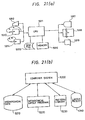
- The following describes the sixth embodiment of this invention with reference to the drawings: Fig. 26 is a functional block diagram showing the automatic electronic circuit layout system, i.e., the cell library, embodying the invention.
Reference number 6100 denotes a computer which stores aprogram 6130 for generating cell layout plans and aprogram 6140 for selecting a plan which meets the condition from among the cell layout plans. By entering the restrictive conditions pertaining to the characteristics and shape of cells using the goaldata input unit 6110, a cell layout selected by theselection program 6140 is produced via the celllayout output unit 6120. - As mentioned previously, the parts layout for analog circuits varies depending on the electrical characteristics of the parts and the shape of layout spaces. The
computer 6100 shown in Fig. 26 realizes a comprehensive cell library by storing a celllayout generation program 6130 for generating the cell layout organically and aprogram 6140 for selecting a cell which meets the purpose and restriction from among the generated layout shapes. Namely, in contrast to a conventional standard cell system in which the cell shape is fixed, the cell shape can be determined quickly using theprograms - Fig. 27 is a flowchart showing the processing of the program shown in Fig. 26. Initially, when the goal specifications and goal shape are entered through the goal
data input unit 6110, the celllayout proposal program 6130 generates cell shapes sequentially and organically (steps 6210, 6220). The cell layoutplan selection program 6140 compares the generated cell shapes with the already generated shape plan, and stores whichever is more consistent with the goal (step 6240). This operation is repeated until all candidates have been tried so that the cell shape which is most consistent with the goal is stored (step 6230). After the selecting process has completed, the stored cell shape most consistent with the goal is retrieved and output via the cell layout output unit 6120 (step 6250). - Fig. 28 is a set of diagrams used to explain the application of this invention in determining the layout shape of a resistor, the simplest component used in an analog circuit. The resistor to be laid out is symbolized as shown by 6310, and is assumed to have a resistance of 100. In designing a layout for this
resistor 6310, various patterns including alinear type 6320,bend type 6330,parallel type 6340, and so on may be used. When the layout of a resistor is intended to be produced in LSI, one of thepatterns 6320―6340 most consistent with the goal will be selected in consideration of the resistance which characterizes theresistor 6310 and the shape of the space where it is to be laid, and the detailed shape of the pattern will be determined. - In Fig. 28,
sections whole sections - The layout shape is defined by the outside dimensions X and Y, the length of element (resistor body) L1, the width of element W1, the base length of contact W2, the height of contact W3, the spacing of elements E, and the number of repetitions of pattern K, as shown in Fig. 28. The variable K has a value of K=2 for the
pattern 6330 of Fig. 28, and K=4 for thepattern 6340. - In this embodiment, the resistance and the goal shape are given to select one of the three patterns which best meets the goal, and to determine the detailed shape of the pattern.
- Fig. 29 is a layout diagram of a wafer to which this invention is applied, and Fig. 30 is a set of diagrams showing the application of this invention for combining cells. In LSI technology, a group of resistors, capacitors, transistors, etc. and the combination thereof is termed a "cell". On the
wafer 641 shown in Fig. 29, a hatchedportion 642 has already been used to lay out a cell, and this invention can conveniently be applied to place resistors in a vacant area of dimensions a by b. - In addition to discrete components such as resistors, this invention is effective for layout shapes of components in a hierarchical arrangement in which a master part includes slave parts by generating various layout shapes of slave parts so that the final characteristics and shape of the master part well matches the goal. For example, in generating a layout of a differential amplifier as shown in Fig. 30(a), the amplifier is segmented into transistors Q1 and Q2, and resistors R1 and R2 to form
cells 651 through 654, and these cells are assembled so that the complete amplifier is consistent in the characteristics and shape with the goal. Accordingly, by the provision of theprogram 6130 for generating layouts of various cells sequentially, a layout shape for a master part including several slave parts can be configured to meet the goal. - Fig. 31 is an explanatory diagram for the input and output program in the inventive cell library. In this embodiment, a logic programming language is used to describe the program. The logic programming language is designed for use in a fifth generation computer, as described in detail in "Clocksin & Mellish 81; Programming in Prolog, Springer-Verlag, 1981", for example.
- Fig. 31 shows as an example program segments corresponding to the goal
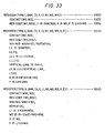
data input unit 6110 and celllayout output unit 6120 in Fig. 26.Line 6400 is an input requesting the generation of a cell layout for a resistor having a resistance of '1000' and dimensions of '5' by '50'.Line 6402 is the corresponding output instructing that a shape "type 1" (patterns convenience type 1,type 2 andtype 3, respectively) be made to have X=5, Y=60, L1=50, W1=1, W2=5, and W3=5. Similarly,lines type 2 is outputted as X=17, Y=18, L1=8, W1=1, W2=5, W3=5, K=2, and E=2.Lines type 3 indicating X=11,Y=11,L1=1,W1=1,W2=11,W3=5,K=3, and E=2. (Although in this embodiment the experiment was conducted using a logic programming language having only the integer processing function, resulting in the inclusion of truncation error in part of the output, such a problem is overcome by running the program using a logic programming language capable of real number processing.) - Figs. 32 and 33 are explanatory diagrams for the inventive cell layout proposal program.
Line 6500 of Fig. 32 represents that the contacts havedimensions 5 by 5,line 6510 represents that the element with a width '1' running for a length of 1 unit on the diffusion layer has a resistance of 20 units.Line 6520 indicates that a resistor created on the diffusion layer has a width of 2 units.Line 6530 and successive lines indicate that a maximum of 10 repetitions are allowable in the arrangement ofpatterns - Fig. 33 is a set of programs for creating the shapes of resistors using data given in Fig. 32. The line block starting with 6600 is a program for creating a pattern of
type 1, the line block from 6610 is a program fortype 2, and the line block from 6640 is a program fortype 3.Line 6602 is a section for making an assumption of the contact size in the data of Fig. 32,line 6604 includes a section for making an assumption of the width of the resistor wire, and the section for calculating the values of L1, X and Y based on these assumptions.Line 6600 is a program involving the resistance "ohm" as an input variable and X, Y, L1, W2 and W3 as an output variables. - Fig. 34 is an explanatory diagram for the inventive cell layout plan selection program. The cell layout
plan selection program 6140 selects one of generated cell layout shapes which matches the purpose, and provides it as a final plan.Line 6700 is a program which enters resistance Ohm and goal shape X-Obj, Y-Obj, and outputs Ans.Line 6702 is a section which stores a dummy shape plan for the comparision online 6240.Line 6704 is a section for creating a layout shape plan for the resistor using the program of Fig. 33.Line 6706 is a section which analyzes the difference between the created shape and the goal shape.Line 6708 is a section which compares the already created plan with the newly created plan and stores the one more consistent with the goal.Line 6710 is a section for creating all alternative shape plans. The sequence returns toline 6700 to repeat the above operations.Line 6740 is a program for outputting the final result, and it corresponds to step 2650 in Fig. 27.Lines programs - A conventional standard cell system, when intended for the layout of analog circuits, is usually merely the storing of fixed shape cells and does not always provide cell options for the circuit characteristics and the shape of part layout areas, whereas the inventive method generates cell layouts to meet restrictions pertaining to the characteristics of circuit components and their layout areas.
- According to the sixth embodiment of this invention, as described above, cell layouts for analog circuits can be generated automatically to meet the restrictions pertaining to the characteristics of circuit components and their layout areas, whereby standard cells for analog circuit can be realized.
- The seventh embodiment of this invention will be described in connection with Fig. 35 showing the software organization of the inventive AOV data retrieval system. This system is realized by
basic functions 7110 andAOV retrieving functions 7120. The basic functions include a tree structure defining function and two more functions, binary trees being used as the tree structure in this embodiment. These functions are named 'binary' (7132), 'delete' and 'recall' in this embodiment. - The AOV retrieving functions include
data reading functions 7150 made up of 3-level functions such as the level-1 reading function named 'fget-a'. Remaining functions are also made up of 3-level functions with appropriate names. - Fig. 36 shows the hardware environment for carrying out this invention. Net data is entered through a
keyboard 72,light pen 73 andtablet 74. The knowledge base and data base are realized using amemory unit 76 andmagnetic disc file 75. The layout result and intermediate result are outputted through adisplay 77,plotter 78 andprinter 79. - The realization of the tree
structure definition functions 7132 shown in Fig. 35 is listed in the following program list (14).
-
Line 200 is a function for retrieving information 'Prop' corresponding to key K from node K(K,P) in the binary tree. Line 210 is a left sub-tree retrieval function, line 220 is a right sub-tree retrieval function, andline 230 is a function for adding a new information node K(K, Prop) to the tree during the void tree retrieval. In the list, 't(X,K(K,Prop), Z)' signifies a binary tree, where X is a left sub-tree, Z is a right sub-tree and K(K, Prop) is a node having key K and information Prop. The term void signifies a void tree. - The following program list (15) shows the function used to delete information from the tree structure.

-
Line 300 indicates that the deletion of node K(K, Prop) in the tree structure t(X,K(K,Prop), void) results in a remainder of X.Lines 310 through 350 are also functions for deleting information in the tree structure. Each function has a deleting method which depends on the property of the tree structure, and a deleting operation is carried out separately for each case. Function 'successor" used on line 320 is a function for removing a successor tree of a node within the tree structure, and its realization is as shown on lines 360 and 370. - The tree structure retrieval function in Fig. 35 is listed in program list (16).

-
Line 400 is a function for finding a node having key 'Key' in the local variable dictionary and outputting its content to 'Ans'. The function uses on its right side the above-mentioned binary function. - The realization of the AOV retrieval function in Fig. 35 is listed in the following program list (17).

-
Line 500 is a function for extracting information using the single-level key "A" from tree structure local variables'Dic' into 'Ans'. Line 505 extracts information using two-level keys 'A' and '0' into 'Ans'. Line 506 extracts information corresponding to three-level keys 'A', '0' and 'V'. Line 515 is a function for transforming an old tree'Dicold' upon the entry of information 'In' corresponding to key'A' into a new tree 'Dicnew'. Lines 520 and 525 are functions with 2-level and 3-level keys. Lines 530 through 540 are functions for deleting part of the tree structure, and lines 545 through 555 are functions for changing part of the tree structure. - The following program list (18) shows examples of using the functions in the program list (17).

- Line 600 signifies that information indicating the base diffusion layer (base-diff) of a transistor (tr1) having a shape [4,5] is added to the tree structure 'Dic1' to form a new tree structure Dic2, and thereafter an inquiry is made as to "what is the shape of base-diff of trl", resulting in a reply of Ans=[4,5]. Line 620 is an example of storing the same information in the tree structure 'Dic2' and, thereafter, changing the shape [4,5] to [6,8], and confirming whether the change has been made correctly. The correct change is shown on line 630.
- As described above, the reason that the inventive system can be realized in the logic language without degrading the efficiency of retrieval is the formation of a tree structure with satisfactory retrieval efficiency in the logic language and realization of the AOV retrieval system using it.
- As described above, this invention enables a significant speedup of retrieving, input modifying and updating graphic information used in CAD systems, data bases of design information and knowledge base though the use of the conventional language. The application of this invention ranges extensively in fields involving data transactions, such as translation, recognition and rule processing, in which enhancement of efficiency is expected.
- This invention realizes the AOV retrieval system in logic languages such as Prolog which is expected to become important in CAD systems and the like in the future, without degrading the retrieval efficiency although it has previously been difficult to realize in such languages from the viewpoint of retrieval efficiency. The invention makes possible an incomparable speedup when compared with the conventional case of converting the program itself into a program which uses global variables.
- When a large number of complex shapes are stored in the computer system and the optimal one is selected by trying several layout plans for a set of shapes, as is commonly seen in layout CAD systems, it is desirable to have both the alternative search function possessed by the logic language and the shape expression ability posessed by the AOV retrieval system.
- This invention accomplishes the purpose.
Claims (7)
Applications Claiming Priority (14)
| Application Number | Priority Date | Filing Date | Title |
|---|---|---|---|
| JP15526184A JPS6134674A (en) | 1984-07-27 | 1984-07-27 | Electronic circuit layout system |
| JP15525784A JPS6134671A (en) | 1984-07-27 | 1984-07-27 | Electronic circuit structure understanding system |
| JP15525984A JPS6134673A (en) | 1984-07-27 | 1984-07-27 | Circuit signal propagation path extracting system |
| JP15525884A JPS6134672A (en) | 1984-07-27 | 1984-07-27 | Circuit structure understanding system |
| JP155261/84 | 1984-07-27 | ||
| JP155259/84 | 1984-07-27 | ||
| JP155257/84 | 1984-07-27 | ||
| JP155258/84 | 1984-07-27 | ||
| JP166050/84 | 1984-08-08 | ||
| JP59166050A JPH0623988B2 (en) | 1984-08-08 | 1984-08-08 | Electronic circuit layout generation method |
| JP59166350A JPH067387B2 (en) | 1984-08-10 | 1984-08-10 | Automatic layout method |
| JP59166349A JPS6145329A (en) | 1984-08-10 | 1984-08-10 | Data transaction system for logical language |
| JP166350/84 | 1984-08-10 | ||
| JP166349/84 | 1984-08-10 |
Publications (3)
| Publication Number | Publication Date |
|---|---|
| EP0169576A2 EP0169576A2 (en) | 1986-01-29 |
| EP0169576A3 EP0169576A3 (en) | 1987-10-21 |
| EP0169576B1 true EP0169576B1 (en) | 1990-12-19 |
Family
ID=27566177
Family Applications (1)
| Application Number | Title | Priority Date | Filing Date |
|---|---|---|---|
| EP85109414A Expired - Lifetime EP0169576B1 (en) | 1984-07-27 | 1985-07-26 | Method and system of circuit pattern understanding and layout |
Country Status (3)
| Country | Link |
|---|---|
| US (1) | US4651284A (en) |
| EP (1) | EP0169576B1 (en) |
| DE (1) | DE3580946D1 (en) |
Families Citing this family (58)
| Publication number | Priority date | Publication date | Assignee | Title |
|---|---|---|---|---|
| US4964060A (en) * | 1985-12-04 | 1990-10-16 | Hartsog Charles H | Computer aided building plan review system and process |
| JPS62159278A (en) * | 1986-01-08 | 1987-07-15 | Hitachi Ltd | Automatic logical designing system |
| US4831543A (en) * | 1986-02-21 | 1989-05-16 | Harris Semiconductor (Patents) Inc. | Hierarchical net list derivation system |
| JPH0785249B2 (en) * | 1986-05-16 | 1995-09-13 | 株式会社日立製作所 | Design support device |
| AU7728187A (en) * | 1986-09-12 | 1988-03-17 | Digital Equipment Corporation | Cad of logic circuits: rule structure for inserting new elements |
| US5191646A (en) * | 1986-11-20 | 1993-03-02 | Hitachi, Ltd. | Display method in software development support system |
| JPS63137327A (en) * | 1986-11-29 | 1988-06-09 | Toshiba Corp | Meaning network device |
| US4849928A (en) * | 1987-01-28 | 1989-07-18 | Hauck Lane T | Logic array programmer |
| US4949388A (en) * | 1987-02-19 | 1990-08-14 | Gtx Corporation | Method and apparatus for recognition of graphic symbols |
| JPH0652502B2 (en) * | 1987-05-06 | 1994-07-06 | 株式会社日立製作所 | Reasoning method |
| US4815003A (en) * | 1987-06-19 | 1989-03-21 | General Electric Company | Structured design method for high density standard cell and macrocell layout of VLSI chips |
| US4852015A (en) * | 1987-06-24 | 1989-07-25 | Eta Systems, Inc. | Automatic circuit layout router |
| JP2535976B2 (en) * | 1987-11-17 | 1996-09-18 | 株式会社日立製作所 | Form connection configuration automatic creation system |
| US4868770A (en) * | 1987-12-02 | 1989-09-19 | Analogy, Inc. | Simulation results enhancement method and system |
| US4922432A (en) * | 1988-01-13 | 1990-05-01 | International Chip Corporation | Knowledge based method and apparatus for designing integrated circuits using functional specifications |
| US4965758A (en) * | 1988-03-01 | 1990-10-23 | Digital Equipment Corporation | Aiding the design of an operation having timing interactions by operating a computer system |
| US5062054A (en) * | 1988-03-10 | 1991-10-29 | Matsushita Electric Industrial Co., Ltd. | Layout pattern generation and geometric processing system for LSI circuits |
| US5031111C1 (en) * | 1988-08-08 | 2001-03-27 | Trw Inc | Automated circuit design method |
| US5239465A (en) * | 1988-10-11 | 1993-08-24 | Hitachi, Ltd. | Method and system for layout design of integrated circuits with a data transferring flow |
| US4965741A (en) * | 1988-10-17 | 1990-10-23 | Ncr Corporation | Method for providing an improved human user interface to a knowledge based system |
| JP2954223B2 (en) * | 1988-11-08 | 1999-09-27 | 富士通株式会社 | Method for manufacturing semiconductor device |
| US5351197A (en) * | 1989-04-13 | 1994-09-27 | Cascade Design Automation Corporation | Method and apparatus for designing the layout of a subcircuit in an integrated circuit |
| US5157668A (en) * | 1989-07-05 | 1992-10-20 | Applied Diagnostics, Inc. | Method and apparatus for locating faults in electronic units |
| US5202841A (en) * | 1989-07-14 | 1993-04-13 | Mitsubishi Denki Kabushiki Kaisha | Layout pattern verification system |
| JP2801931B2 (en) * | 1989-09-07 | 1998-09-21 | 松下電器産業株式会社 | Logic design processing device, circuit conversion rule translation device, and circuit conversion rule translation method |
| US5367468A (en) * | 1990-02-21 | 1994-11-22 | Kabushiki Kaisha Toshiba | Design aid method and design aid apparatus for integrated circuits |
| US5490232A (en) * | 1990-10-25 | 1996-02-06 | Daiwa House Industry Co., Ltd. | Computer-aided thought process simulation design system |
| US5459673A (en) * | 1990-10-29 | 1995-10-17 | Ross Technology, Inc. | Method and apparatus for optimizing electronic circuits |
| US5299139A (en) * | 1991-06-21 | 1994-03-29 | Cadence Design Systems, Inc. | Short locator method |
| US5471398A (en) * | 1991-07-01 | 1995-11-28 | Texas Instruments Incorporated | MTOL software tool for converting an RTL behavioral model into layout information comprising bounding boxes and an associated interconnect netlist |
| US5293479A (en) * | 1991-07-08 | 1994-03-08 | Quintero Smith Incorporated | Design tool and method for preparing parametric assemblies |
| US5347465A (en) * | 1992-05-12 | 1994-09-13 | International Business Machines Corporation | Method of integrated circuit chips design |
| EP0597087B1 (en) * | 1992-06-02 | 1999-07-28 | Hewlett-Packard Company | Computer-aided design method for multilevel interconnect technologies |
| US5493504A (en) * | 1992-10-28 | 1996-02-20 | Nippon Telegraph And Telephone Corporation | System and method for processing logic function and fault diagnosis using binary tree representation |
| US5587918A (en) * | 1992-12-28 | 1996-12-24 | Kabushiki Kaisha Toshiba | Circuit pattern comparison apparatus |
| US5519633A (en) * | 1993-03-08 | 1996-05-21 | International Business Machines Corporation | Method and apparatus for the cross-sectional design of multi-layer printed circuit boards |
| US5475804A (en) * | 1993-06-18 | 1995-12-12 | Motorola, Inc. | Electronics circuit graphics symbol scaling method |
| US5818726A (en) * | 1994-04-18 | 1998-10-06 | Cadence Design Systems, Inc. | System and method for determining acceptable logic cell locations and generating a legal location structure |
| US5764534A (en) * | 1994-10-13 | 1998-06-09 | Xilinx, Inc. | Method for providing placement information during design entry |
| US7068270B1 (en) * | 1994-12-02 | 2006-06-27 | Texas Instruments Incorporated | Design of integrated circuit package using parametric solids modeller |
| JP2800881B2 (en) * | 1995-07-31 | 1998-09-21 | 日本電気株式会社 | Wiring parasitic load calculation method |
| US6321367B1 (en) * | 1996-08-30 | 2001-11-20 | Altera Corporation | Apparatus and method for automatically generating circuit layouts |
| US5914889A (en) * | 1996-09-13 | 1999-06-22 | Lucent Technologies Inc. | Method and system for generating a mask layout of an optical integrated circuit |
| DE19711909C2 (en) * | 1997-03-21 | 1999-01-07 | Siemens Ag | Method for determining the processing sequence of program modules simulating circuit components using a network list |
| US6577992B1 (en) | 1999-05-07 | 2003-06-10 | Nassda Corporation | Transistor level circuit simulator using hierarchical data |
| US6405351B1 (en) | 2000-06-27 | 2002-06-11 | Texas Instruments Incorporated | System for verifying leaf-cell circuit properties |
| US6606732B2 (en) | 2000-12-11 | 2003-08-12 | International Business Machines Corporation | Method for specifying, identifying, selecting or verifying differential signal pairs on IC packages |
| JP2002252161A (en) * | 2001-02-23 | 2002-09-06 | Hitachi Ltd | Semiconductor manufacturing system |
| US7024640B2 (en) * | 2001-06-29 | 2006-04-04 | Koninklijke Philips Electronics N.V. | Integrated circuit cell identification |
| US6978012B2 (en) * | 2002-01-02 | 2005-12-20 | Intel Corporation | Echo cancellation using a variable offset comparator |
| US20040103375A1 (en) * | 2002-11-27 | 2004-05-27 | Rutie Chen | Method and apparatus for automated schematic rendering |
| US20050033662A1 (en) * | 2003-08-04 | 2005-02-10 | James Buch | Method for visualizing differing types of window coverings within a room setting |
| JP2005202928A (en) * | 2003-12-19 | 2005-07-28 | Fujitsu Ltd | Layout processor, layout processing method and program |
| US20080148200A1 (en) * | 2006-12-14 | 2008-06-19 | Christian Von Mueffling | Method for checking the layout of an integrated circuit |
| US7818710B2 (en) * | 2007-07-03 | 2010-10-19 | Micron Technology, Inc. | Method and system for lithographic simulation and verification |
| WO2015053852A1 (en) | 2013-10-07 | 2015-04-16 | Parviz Saghizadeh | Complex layout-based topological data analysis of analog netlists to extract hierarchy and functionality |
| US9830414B2 (en) | 2014-06-16 | 2017-11-28 | Raytheon Company | Pattern matching techniques in analog and mixed signal circuits |
| US10192018B1 (en) * | 2016-03-31 | 2019-01-29 | Cadence Design Systems, Inc. | Method and system for implementing efficient trim data representation for an electronic design |
Family Cites Families (3)
| Publication number | Priority date | Publication date | Assignee | Title |
|---|---|---|---|---|
| US4055802A (en) * | 1976-08-12 | 1977-10-25 | Bell Telephone Laboratories, Incorporated | Electrical identification of multiply configurable circuit array |
| US4613940A (en) * | 1982-11-09 | 1986-09-23 | International Microelectronic Products | Method and structure for use in designing and building electronic systems in integrated circuits |
| US4554625A (en) * | 1983-06-14 | 1985-11-19 | International Business Machines Corporation | Method for generating an optimized nested arrangement of constrained rectangles |
-
1985
- 1985-07-26 EP EP85109414A patent/EP0169576B1/en not_active Expired - Lifetime
- 1985-07-26 DE DE8585109414T patent/DE3580946D1/en not_active Expired - Lifetime
- 1985-07-26 US US06/759,134 patent/US4651284A/en not_active Expired - Lifetime
Also Published As
| Publication number | Publication date |
|---|---|
| US4651284A (en) | 1987-03-17 |
| EP0169576A2 (en) | 1986-01-29 |
| EP0169576A3 (en) | 1987-10-21 |
| DE3580946D1 (en) | 1991-01-31 |
Similar Documents
| Publication | Publication Date | Title |
|---|---|---|
| EP0169576B1 (en) | Method and system of circuit pattern understanding and layout | |
| US5212650A (en) | Procedure and data structure for synthesis and transformation of logic circuit designs | |
| US5559718A (en) | System and method for model-based verification of local design rules | |
| US5267175A (en) | Data base access mechanism for rules utilized by a synthesis procedure for logic circuit design | |
| Weste | Virtual grid symbolic layout | |
| US7206731B2 (en) | Electromagnetic/circuit co-simulation and co-optimization with parametric layout components | |
| US5381343A (en) | Hier archical pitchmaking compaction method and system for integrated circuit design | |
| US4831543A (en) | Hierarchical net list derivation system | |
| US8473885B2 (en) | Physical design system and method | |
| US5351197A (en) | Method and apparatus for designing the layout of a subcircuit in an integrated circuit | |
| US6374200B1 (en) | Layout apparatus for laying out objects in space and method thereof | |
| EP0259703A2 (en) | Rule structure for insertion of new elements in a circuit design synthesis procedure | |
| US6298469B1 (en) | Method and system for allowing an integrated circuit to be portably generated from one manufacturing process to another | |
| Kim et al. | Exploiting domain knowledge in IC cell layout | |
| US6532582B1 (en) | Method and apparatus for optimal critical netlist area selection | |
| Su et al. | HPEX: A hierarchical parasitic circuit extractor | |
| Richard | A standard cell initial placement strategy | |
| EP0262397A2 (en) | Procedure and data structure for synthesis and transformation of logic circuit designs | |
| Mani et al. | Using genetic algorithm for slicing floorplan area optimization in circuit design | |
| EP1010109B1 (en) | A method for storing of layout data, routing method and electronic device | |
| Dutton | Stanford overview in VLSI research | |
| Beyls et al. | A design methodology based upon symbolic layout and integrated CAD tools | |
| Dobes | A multi-contouring algorithm | |
| Evans et al. | ADL: An algorithmic design language for integrated circuit synthesis | |
| Iimura | iCHARM: Hierarchical CMOS circuit extraction with power bus extraction |
Legal Events
| Date | Code | Title | Description |
|---|---|---|---|
| PUAI | Public reference made under article 153(3) epc to a published international application that has entered the european phase |
Free format text: ORIGINAL CODE: 0009012 |
|
| AK | Designated contracting states |
Designated state(s): DE FR GB |
|
| PUAL | Search report despatched |
Free format text: ORIGINAL CODE: 0009013 |
|
| AK | Designated contracting states |
Kind code of ref document: A3 Designated state(s): DE FR GB |
|
| 17P | Request for examination filed |
Effective date: 19880229 |
|
| 17Q | First examination report despatched |
Effective date: 19890713 |
|
| GRAA | (expected) grant |
Free format text: ORIGINAL CODE: 0009210 |
|
| AK | Designated contracting states |
Kind code of ref document: B1 Designated state(s): DE FR GB |
|
| REF | Corresponds to: |
Ref document number: 3580946 Country of ref document: DE Date of ref document: 19910131 |
|
| ET | Fr: translation filed | ||
| PLBE | No opposition filed within time limit |
Free format text: ORIGINAL CODE: 0009261 |
|
| STAA | Information on the status of an ep patent application or granted ep patent |
Free format text: STATUS: NO OPPOSITION FILED WITHIN TIME LIMIT |
|
| 26N | No opposition filed | ||
| PGFP | Annual fee paid to national office [announced via postgrant information from national office to epo] |
Ref country code: FR Payment date: 19980710 Year of fee payment: 14 |
|
| PGFP | Annual fee paid to national office [announced via postgrant information from national office to epo] |
Ref country code: GB Payment date: 19980716 Year of fee payment: 14 |
|
| PGFP | Annual fee paid to national office [announced via postgrant information from national office to epo] |
Ref country code: DE Payment date: 19980928 Year of fee payment: 14 |
|
| PG25 | Lapsed in a contracting state [announced via postgrant information from national office to epo] |
Ref country code: GB Free format text: LAPSE BECAUSE OF NON-PAYMENT OF DUE FEES Effective date: 19990726 |
|
| PG25 | Lapsed in a contracting state [announced via postgrant information from national office to epo] |
Ref country code: FR Free format text: THE PATENT HAS BEEN ANNULLED BY A DECISION OF A NATIONAL AUTHORITY Effective date: 19990731 |
|
| GBPC | Gb: european patent ceased through non-payment of renewal fee |
Effective date: 19990726 |
|
| PG25 | Lapsed in a contracting state [announced via postgrant information from national office to epo] |
Ref country code: DE Free format text: LAPSE BECAUSE OF NON-PAYMENT OF DUE FEES Effective date: 20000503 |
|
| REG | Reference to a national code |
Ref country code: FR Ref legal event code: ST |