EP0179665B1 - Apparatus and method for magnetron-enhanced plasma-assisted chemical vapor deposition - Google Patents
Apparatus and method for magnetron-enhanced plasma-assisted chemical vapor deposition Download PDFInfo
- Publication number
- EP0179665B1 EP0179665B1 EP85307699A EP85307699A EP0179665B1 EP 0179665 B1 EP0179665 B1 EP 0179665B1 EP 85307699 A EP85307699 A EP 85307699A EP 85307699 A EP85307699 A EP 85307699A EP 0179665 B1 EP0179665 B1 EP 0179665B1
- Authority
- EP
- European Patent Office
- Prior art keywords
- deposition
- films
- plasma
- magnetic field
- film
- Prior art date
- Legal status (The legal status is an assumption and is not a legal conclusion. Google has not performed a legal analysis and makes no representation as to the accuracy of the status listed.)
- Expired - Lifetime
Links
Classifications
-
- H—ELECTRICITY
- H01—ELECTRIC ELEMENTS
- H01J—ELECTRIC DISCHARGE TUBES OR DISCHARGE LAMPS
- H01J37/00—Discharge tubes with provision for introducing objects or material to be exposed to the discharge, e.g. for the purpose of examination or processing thereof
- H01J37/32—Gas-filled discharge tubes
- H01J37/32431—Constructional details of the reactor
- H01J37/32623—Mechanical discharge control means
-
- C—CHEMISTRY; METALLURGY
- C23—COATING METALLIC MATERIAL; COATING MATERIAL WITH METALLIC MATERIAL; CHEMICAL SURFACE TREATMENT; DIFFUSION TREATMENT OF METALLIC MATERIAL; COATING BY VACUUM EVAPORATION, BY SPUTTERING, BY ION IMPLANTATION OR BY CHEMICAL VAPOUR DEPOSITION, IN GENERAL; INHIBITING CORROSION OF METALLIC MATERIAL OR INCRUSTATION IN GENERAL
- C23C—COATING METALLIC MATERIAL; COATING MATERIAL WITH METALLIC MATERIAL; SURFACE TREATMENT OF METALLIC MATERIAL BY DIFFUSION INTO THE SURFACE, BY CHEMICAL CONVERSION OR SUBSTITUTION; COATING BY VACUUM EVAPORATION, BY SPUTTERING, BY ION IMPLANTATION OR BY CHEMICAL VAPOUR DEPOSITION, IN GENERAL
- C23C16/00—Chemical coating by decomposition of gaseous compounds, without leaving reaction products of surface material in the coating, i.e. chemical vapour deposition [CVD] processes
- C23C16/04—Coating on selected surface areas, e.g. using masks
- C23C16/045—Coating cavities or hollow spaces, e.g. interior of tubes; Infiltration of porous substrates
-
- C—CHEMISTRY; METALLURGY
- C23—COATING METALLIC MATERIAL; COATING MATERIAL WITH METALLIC MATERIAL; CHEMICAL SURFACE TREATMENT; DIFFUSION TREATMENT OF METALLIC MATERIAL; COATING BY VACUUM EVAPORATION, BY SPUTTERING, BY ION IMPLANTATION OR BY CHEMICAL VAPOUR DEPOSITION, IN GENERAL; INHIBITING CORROSION OF METALLIC MATERIAL OR INCRUSTATION IN GENERAL
- C23C—COATING METALLIC MATERIAL; COATING MATERIAL WITH METALLIC MATERIAL; SURFACE TREATMENT OF METALLIC MATERIAL BY DIFFUSION INTO THE SURFACE, BY CHEMICAL CONVERSION OR SUBSTITUTION; COATING BY VACUUM EVAPORATION, BY SPUTTERING, BY ION IMPLANTATION OR BY CHEMICAL VAPOUR DEPOSITION, IN GENERAL
- C23C16/00—Chemical coating by decomposition of gaseous compounds, without leaving reaction products of surface material in the coating, i.e. chemical vapour deposition [CVD] processes
- C23C16/44—Chemical coating by decomposition of gaseous compounds, without leaving reaction products of surface material in the coating, i.e. chemical vapour deposition [CVD] processes characterised by the method of coating
- C23C16/455—Chemical coating by decomposition of gaseous compounds, without leaving reaction products of surface material in the coating, i.e. chemical vapour deposition [CVD] processes characterised by the method of coating characterised by the method used for introducing gases into reaction chamber or for modifying gas flows in reaction chamber
- C23C16/45563—Gas nozzles
- C23C16/4558—Perforated rings
-
- C—CHEMISTRY; METALLURGY
- C23—COATING METALLIC MATERIAL; COATING MATERIAL WITH METALLIC MATERIAL; CHEMICAL SURFACE TREATMENT; DIFFUSION TREATMENT OF METALLIC MATERIAL; COATING BY VACUUM EVAPORATION, BY SPUTTERING, BY ION IMPLANTATION OR BY CHEMICAL VAPOUR DEPOSITION, IN GENERAL; INHIBITING CORROSION OF METALLIC MATERIAL OR INCRUSTATION IN GENERAL
- C23C—COATING METALLIC MATERIAL; COATING MATERIAL WITH METALLIC MATERIAL; SURFACE TREATMENT OF METALLIC MATERIAL BY DIFFUSION INTO THE SURFACE, BY CHEMICAL CONVERSION OR SUBSTITUTION; COATING BY VACUUM EVAPORATION, BY SPUTTERING, BY ION IMPLANTATION OR BY CHEMICAL VAPOUR DEPOSITION, IN GENERAL
- C23C16/00—Chemical coating by decomposition of gaseous compounds, without leaving reaction products of surface material in the coating, i.e. chemical vapour deposition [CVD] processes
- C23C16/44—Chemical coating by decomposition of gaseous compounds, without leaving reaction products of surface material in the coating, i.e. chemical vapour deposition [CVD] processes characterised by the method of coating
- C23C16/50—Chemical coating by decomposition of gaseous compounds, without leaving reaction products of surface material in the coating, i.e. chemical vapour deposition [CVD] processes characterised by the method of coating using electric discharges
- C23C16/505—Chemical coating by decomposition of gaseous compounds, without leaving reaction products of surface material in the coating, i.e. chemical vapour deposition [CVD] processes characterised by the method of coating using electric discharges using radio frequency discharges
- C23C16/509—Chemical coating by decomposition of gaseous compounds, without leaving reaction products of surface material in the coating, i.e. chemical vapour deposition [CVD] processes characterised by the method of coating using electric discharges using radio frequency discharges using internal electrodes
-
- C—CHEMISTRY; METALLURGY
- C23—COATING METALLIC MATERIAL; COATING MATERIAL WITH METALLIC MATERIAL; CHEMICAL SURFACE TREATMENT; DIFFUSION TREATMENT OF METALLIC MATERIAL; COATING BY VACUUM EVAPORATION, BY SPUTTERING, BY ION IMPLANTATION OR BY CHEMICAL VAPOUR DEPOSITION, IN GENERAL; INHIBITING CORROSION OF METALLIC MATERIAL OR INCRUSTATION IN GENERAL
- C23C—COATING METALLIC MATERIAL; COATING MATERIAL WITH METALLIC MATERIAL; SURFACE TREATMENT OF METALLIC MATERIAL BY DIFFUSION INTO THE SURFACE, BY CHEMICAL CONVERSION OR SUBSTITUTION; COATING BY VACUUM EVAPORATION, BY SPUTTERING, BY ION IMPLANTATION OR BY CHEMICAL VAPOUR DEPOSITION, IN GENERAL
- C23C16/00—Chemical coating by decomposition of gaseous compounds, without leaving reaction products of surface material in the coating, i.e. chemical vapour deposition [CVD] processes
- C23C16/44—Chemical coating by decomposition of gaseous compounds, without leaving reaction products of surface material in the coating, i.e. chemical vapour deposition [CVD] processes characterised by the method of coating
- C23C16/50—Chemical coating by decomposition of gaseous compounds, without leaving reaction products of surface material in the coating, i.e. chemical vapour deposition [CVD] processes characterised by the method of coating using electric discharges
- C23C16/517—Chemical coating by decomposition of gaseous compounds, without leaving reaction products of surface material in the coating, i.e. chemical vapour deposition [CVD] processes characterised by the method of coating using electric discharges using a combination of discharges covered by two or more of groups C23C16/503 - C23C16/515
-
- H—ELECTRICITY
- H01—ELECTRIC ELEMENTS
- H01J—ELECTRIC DISCHARGE TUBES OR DISCHARGE LAMPS
- H01J37/00—Discharge tubes with provision for introducing objects or material to be exposed to the discharge, e.g. for the purpose of examination or processing thereof
- H01J37/32—Gas-filled discharge tubes
- H01J37/32431—Constructional details of the reactor
- H01J37/3266—Magnetic control means
-
- H—ELECTRICITY
- H01—ELECTRIC ELEMENTS
- H01J—ELECTRIC DISCHARGE TUBES OR DISCHARGE LAMPS
- H01J37/00—Discharge tubes with provision for introducing objects or material to be exposed to the discharge, e.g. for the purpose of examination or processing thereof
- H01J37/32—Gas-filled discharge tubes
- H01J37/32917—Plasma diagnostics
- H01J37/32935—Monitoring and controlling tubes by information coming from the object and/or discharge
-
- H—ELECTRICITY
- H01—ELECTRIC ELEMENTS
- H01J—ELECTRIC DISCHARGE TUBES OR DISCHARGE LAMPS
- H01J2237/00—Discharge tubes exposing object to beam, e.g. for analysis treatment, etching, imaging
- H01J2237/32—Processing objects by plasma generation
- H01J2237/33—Processing objects by plasma generation characterised by the type of processing
- H01J2237/332—Coating
- H01J2237/3322—Problems associated with coating
- H01J2237/3327—Coating high aspect ratio workpieces
Landscapes
- Chemical & Material Sciences (AREA)
- Engineering & Computer Science (AREA)
- Physics & Mathematics (AREA)
- Plasma & Fusion (AREA)
- Materials Engineering (AREA)
- Chemical Kinetics & Catalysis (AREA)
- General Chemical & Material Sciences (AREA)
- Mechanical Engineering (AREA)
- Metallurgy (AREA)
- Organic Chemistry (AREA)
- Analytical Chemistry (AREA)
- Chemical Vapour Deposition (AREA)
- Formation Of Insulating Films (AREA)
- Physical Deposition Of Substances That Are Components Of Semiconductor Devices (AREA)
Description
- In one aspect, the present invention relates to magnetron-enhanced plasma-assisted chemical vapor deposition (CVD) reactors and associated methods for performing high rate deposition of dielectric, semiconductor and conductor films. In addition, the technique can be used for low temperature nitridation and oxidation. In still other aspects, the invention relates to apparatus and methods for performing in-situ multiple integrated circuit processing steps, and to deposition techniques for implementing conformal coatings and planarization.
- The early gas chemistry deposition techniques which were applied to semiconductor integrated circuit fabrication used thermally-activated chemistry to deposit from a gas onto a heated substrate. Such chemical vapor deposition (CVD) of a solid onto a surface involves a heterogeneous surface reaction of gaseous species that adsorb onto the surface. The rate of film growth and the film quality depend on the surface temperature and on the gaseous species available.
- More recently, plasma-enhanced low temperature deposition (and etching) techniques have been developed for depositing diverse materials, including metals such as aluminum and tungsten, dielectric films such as silicon nitride and silicon dioxide, and semiconductor films such as silicon.
- The plasma used in the plasma-assisted CVD processes is a low pressure reactant gas discharge which is developed in an RF field. The plasma is, by definition, an electrically neutral ionized gas in which there are equal number densities of electrons and ions. At the relatively low pressures used in plasma-assisted CVD, the discharge is in the "glow" region and the electron energies can be quite high relative to heavy particle energies. The very high electron temperatures increase the density of disassociated species within the plasma which are available for deposition on nearby surfaces (such as substrates). The enhanced supply of reactive free radicals makes possible the deposition of dense, good quality films at lower temperatures and at faster deposition rates (30-40 nm per minute) (300-400 Angstroms per minute) than are possible using purely thermally-activated processes (10-20 nm per minute) (100-200 Angstroms per minute). However, the deposition rates available using plasma-enhanced processes are still relatively low. In addition, there are other difficulties associated with chemical vapor deposition and plasma-enhanced CVD processes. These difficulties are discussed below.
- Using plasma-assisted chemical vapor deposition, silicon nitride is formed from silane, nitrogen and ammonia reactants as follows:

- The trend toward ever greater device densities and smaller minimum feature sizes and smaller separations in VLSI integrated circuits imposes increasingly stringent requirements on the basic IC fabrication steps of masking, film formation (by deposition or growth), doping and etching. For example, it becomes increasingly difficult to form conformal coatings on stepped surface topography or to achieve planarization of interlevel dielectric layers, even when using plasma-enhanced CVD films. FIG. 1 represents a typical cross-section of an IC step topography in which a first film such as a conductor layer 11 has been formed over the existing stepped topography of a partially completed integrated circuit (not shown) and is undergoing the deposition of an interlayer dielectric layer 12 such as silicon dioxide. This is done preparatory to the formation of a second level conductor layer (not shown). Typically, where the mean free path of the depositing active species is long compared to the step dimensions, (and where there is no rapid surface migration) the deposition rates at the bottom 13, sides 14 and top 15 of the step topography are proportional to the associated arrival angles. Since the bottom surface arrival angle is a function of the depth and width of the trench, the thickness of the deposited layer at the bottom 13 of the trench tends to be less than that at the sides 14 which, in turn, is less than the thickness at the top 15.
- Increasing the pressure used in the deposition process would increase the collision rate of the active species and decrease the mean free path. This would increase the effective size of the arrival angles and increase the deposition rate at the side walls 14 and bottom 13 of the trench. However, and referring to FIG. 2A, this would also increase the arrival angle and associated deposition rate at the step corners 16. For steps separated by a wide trench, the resulting inwardly-sloped film configuration and the associated cusps 17 provide a less than ideal coverage. Nonetheless, the film topography can be made planar (to facilitate formation of the subsequent second level conductor layer) by the use of conventional planarization techniques. In contrast, and referring to FIG. 2B, where the steps are separated by a narrow trench, for example in dense 256 kilobit VLSI structures, the increased deposition rate at the corners 16 encloses a void 18. The void is exposed by a subsequent planarization procedure and allows the second level conductor to penetrate and run along the void and short the conductors and devices along the void.
- Thus, the current state-of-the-art of the plasma-assisted CVD technique can be summarized as follows. Plasma-assisted CVD reactors provide maximum deposition rates of approximately 30-40 nm (300 - 400 Angstroms). However, problems exist in meeting the needs of future plasma deposition technology, for example in eliminating or decreasing high hydrogen impurity levels in plasma CVD nitride films and in the difficulty in achieving conformal step coverage and effective planarization in the topography of small- dimension VLSI devices.
- The requirements for any successful future plasma deposition technology are several. The capability for forming low hydrogen silicon nitride and the requirements of topography in terms of step coverage and planarization have been mentioned. In addition, the capability for forming interlevel plasma oxide films as well as low hydrogen-content oxynitride films is desirable. Oxynitride films have different dielectric properties from oxides and nitrides and are being implemented as gate dielectrics in both volatile and nonvolatile IC technologies. Furthermore, it is desirable to have the capability to form interconnects and metalization of materials such as silicides, aluminum and refractory metals. Increasingly, and in particular as multi-level mask conductor and dielectric structures are implemented, it is desirable to have an in-situ process which is capable of performing a multiplicity of steps without removing the wafer from the chamber by simply changing the reactant gas chemistry and operation conditions. This latter statement is demonstrated by two examples.
- Consider first the use of silicon nitride as a passivation layer. As mentioned, low-hydrogen content nitride is desirable to eliminate hot carrier problems, but low-hydrogen nitride films can be highly stressed. One approach which permits the use of low-hydrogen nitride passivation layers is to first deposit phosphosilicate glass (PSG) to alleviate the stress, then deposit the low-hydrogen content nitride. Obviously, throughput would be increased and the defect density would be decreased if the two deposition steps could be performed in the same reactor.
- A second example involves the use of aluminum. Sputter-deposited aluminum is the favorite metal for interconnects despite the several problems associated with its use. For example, pure aluminum undergoes electromigration which causes cracks, voids, etc. Aluminum also forms hillocks or columns which can punch through insulating layers. It is possible to dope aluminum with copper to decrease electromigration, but copper itself is very hard to etch. A better solution is to form a multi-layer structure of alumi- num/tungsten/aluminum. Again, throughput would be increased by using chemical vapor deposition to deposit the three layers in the same reactor. Perhaps more important than all is that CVD aluminum will have much better step-coverage than sputter-deposited aluminum films.
- Furthermore, in implementing the dense, complex, process-sensitive present and future integrated circuits structures, it is and will be desirable to have a plasma deposition technology which is adaptable to automatic cassette-to-cassette wafer handling, both for off-loading wafers from the cassette into the processing chamber and returning the wafers to the cassette after processing.
- Finally, throughput and particulate control will be helped by the use of load lock mechanisms. Load lock mechanisms not only decrease pumping and processing time, but also decrease exposure of the very susceptible VLSI structures to contaminants.
- In view of the above discussion, it is an object of the present invention to provide apparatus and methods for high-rate plasma deposition of dielectric and metal and semiconductor films.
- The above and other objectives are accomplished by the application of a magnetic field to assist and enhance plasma chemical vapor deposition. The application of magnetic fields parallel to a work surface is known to be efficient in magnetron solid sputtering technology and in gas chemistry etching, but previously has not been applied to gas chemistry deposition. The low pressures required in gas chemistry processes conventionally permit only a low concentration of plasma reactant species and a corresponding low deposition rate. However, we have found that the appropriate application of a magnetic field in conjunction with plasma CVD techniques provides very high deposition rates of dense, high quality films at very low pressure and low substrate temperatures and with excellent uniformity. The technique is applicable to the deposition of a wide range of metal, insulator and conductor film compositions, including the formation of low-hydrogen-content silicon nitride films at high deposition rates, and is uniquely suited to the formation of conformal films.
- This invention provides a plasma reactor for depositing a film on a substantially planar substrate, comprising: a vacuum chamber having a gas inlet adapted for introducing a reaction gas mixture into the chamber; an electrode mounted within the chamber, the electrode having a substantially planar face, and being adapted for receiving RF energy from an RF power supply so as to excite the gas mixture into a plasma state and thereby create an electric field between the plasma and the electrode; means for mounting the substrate on the electrode with the substrate lying parallel to the face of the electrode, whereby the electric field is perpendicular to the plane of the substrate; and a magnetic assembly for producing a magnetic field which is parallel to the substrate; wherein the magnetic assembly is adapted to produce a magnetic field which is perpendicular to the electric field at the substrate and is substantially uniform in magnitude and direction throughout the chamber.
- Preferably first and second reflectors are mounted adjacent opposite ends of the electrode and oriented perpendicular to the electrode face, the reflectors being composed of an electrically conductive, non-magnetic material.
- More specifically the magnet assembly which provides said uniform magnetic field comprises an electromagnet to enable the field strength to be varied.
- In any of the above arrangements the magnet assembly may comprise an electromagnet providing North and South poles reversible by reversing the current supply.
- Also in any of the above arrangements the magnet assembly may comprise first and second electromagnet coils positioned parallel to each other at opposite ends of the chambers.
- In the latter arrangement the first and second electromagnet coils may each have a diameter approximately equal to twice the distance between them.
- The invention also provides a process for depositing a film on a substrate, comprising the steps of: supplying a reaction gas mixture in to a vaccum chamber; supplying RF energy to an electrode within the chamber so as to excite the gas mixture into a plasma state and thereby create an electric field between the plasma and the electrode; and mounting the substrate parallel to, and closely adjacent to, a planar face of the electrode, whereby the plane of the substrate is perpendicular to the electric field; and producing a magnetic field which is parallel to the substrate; wherein the magnetic field produced is perpendicular to the electric field at the substrate, and substantially uniform in magnitude and direction throughout the cross-section of the chamber.
- More particularly the step of producing a magnetic field may further comprise varying the magnetic field strength while the film is being deposited on the substrate.
- The step of producing a magnetic field may further comprise varying the frequency of the magnetic field while the film is being deposited on the substrate.
- In any of the above methods the step of supplying a reaction gas mixture may include supplying an etching gas to etch the film while it is being deposited.
- In the latter case the method may also include the step of increasing the proportion of etching gas in the gas mixture after a time when the film deposition is nearing completion.
- The above and other aspects of the present invention are described in conjunction with the drawings, in which:
- FIG. 1 is a schematic cross-sectional representation of an integrated circuit which illustrates the arrival angles associated with the deposition of a layer of material such as dielectric onto a surface of stepped topography;
- FIGS. 2A and 2B are schematic cross-sections, similar to FIG. 1, which illustrate the effect of trench width on planarization;
- FIG. 3 is a perspective view, partly in schematic form and partially cut-away, of a magnetron reaction system which is constructed in accordance with the principles of the present invention;
- FIG. 4 is a cross-sectional view of the reactor of FIG. 3;
- FIG. 5 is an enlarged partial view of the electrode cross-section shown in FIG. 4, schematically illustrating the magnetic field lines which confine electrons adjacent the electrode surface;
- FIGS. 6A, 6B and 6C illustrate the intensity of the spectral response of the active nitrogen species present in the plasma at different values of the magnetic field;
- FIGS. 7 and 8 graphically illustrate silicon nitride deposition rates as a function of magnetic field and total reactant gas flow, respectively, for selected operating conditions of the reactor system of FIG. 3;
- FIG. 9 graphically illustrates DC bias as a function of magnetic field for selected operating conditions of the reactor system of FIG. 3;
- FIGS. 10 and 11 graphically illustrate DC bias voltage us a function of pressure for selected operating conditions of the reactor system of FIG. 3; and
- FIG. 12 is a cross-section of the surface topology of an integrated circuit, in the manner of FIG. 1, illustrating the conformal, planar qualities of oxide and nitride films deposited using the reactor system of FIG. 3.
- FIG. 3 illustrates a magnetron reaction system 30 which is constructed in accordance with the present invention. The system 30 includes a cylindrical stainless steel vacuum chamber 31 which mounts a band cathode assembly 32 therein. The cathode 32 is insulatingly mounted within and insulated from the chamber 31 by insulating mounting posts 33-33. In a preferred embodiment, the cathode 32 comprises a central axial section 34 and inner end reflector sections 36-36 which are formed of aluminum or other conductive non-magnetic material. Outer end sections 37-37 are formed of insulating material, such as Maycor@. Power is supplied for effecting plasma operation by an RF system 38 which includes an RF power supply and load matching network, and is connected to the cathode 32 by insulated power lead 39.
- Reactant gas is applied to the chamber 31 by one or more gas manifold rings 41 via an inlet shaft 42 from a gas supply system. This system includes a number of gas storage tanks or reservoirs 43-43 which supply gases through line 42 to the inlet manifold ring 41.
- Referring also to the cross-sectional view of the cathode 34 and inlet manifold ring 41 shown in FIG. 4, a semiconductor wafer is positioned by means 44, such as clips, to the side of the cathode (or may be mounted or held within a recess (not shown) in the cathode). In a presently preferred arrangement, a gas ring 41 is provided for each wafer or substrate 5. Alternatively, the gas ring can be mounted on the cathode. The diameter of the gas ring 41 is slightly larger than the diameter of the associated substrate 5 and the ring apertures 46 are formed toward the inside of the ring so that the manifold directs reactant gas at a slight angle onto the substrate. This provides an even gas flow across the substrate surface and off the substrate, through the ring and to an exhaust outlet 47 in the chamber wall which is aligned with the ring and the wafer. The outlet 47 is connected to a mechanical pump (not shown) via a vacuum valve and Roots blower. This arrangement facilitates uniform coverage and processing of the substrate by the reactant gas. This arrangement also decreases the inherent tendency of reaction chambers to form on the relatively cool inner chamber walls deposits which can be redeposited on the substrate as contaminants. While other inlet means can be used, such as nozzles and apertured flat manifolds, the ring configuration is preferred for its uniform gas distribution and suppression of wall deposits. Control of the system can be provided via a capacitance manometer sensor which operates through a pressure control system and DC motor to control the speed of the blower.
- Although only one substrate 5, inlet manifold 41 and exhaust outlet 47 are shown in FIG. 3 to facilitate illustration, preferably two of each (or more) are used, as shown in FIG. 4. The number used depends upon the available mounting space or surfaces in the particular implementation of the cathode 32. Typically the cathode has a two-sided configuration as shown in FIGS. 3 and 4, or is a polygon. However, as described below, the magnetic field within the chamber is uniform and as a consequence other electrode shapes can be used.
- The system 30 is operable to deposit films at room temperature, i.e. without heating of the substrate 5 by means other than the deposition reaction. However, as shown in the cross-sectional view of FIG. 4, in one working embodiment, the cathode body 34 has heating means 52 therein, such as an electric resistance filament for uniformly heating the substrates 5 to enhance film quality. The maximum heating requirements, 250 ° C, are lower than the temperatures used in plasma CVD. The RF energy could be used to heat the substrate support and the substrate. Cooling fluid, such as nitrogen gas, can also be provided to the interior of the cathode body 34 to facilitate control of the substrate temperature.
- Electro-magnets 54-55, typically formed of copper coil (not shown), are circumferentially positioned about the chamber 31 near the top and bottom thereof. The electro-magnets form north and south poles which are reversible by reversing the coil current. In particular, the chamber dimensions and coils form a Helmholtz configuration in which the coil separation, which is precisely maintained by mounting standoffs 56-56, is approximately one-half the coil diameter. In this configuration, the electromagnets form a uniform magnetic field over substantially the entire diametrical cross-section of the chamber. The parallel magnetic field lines, indicated by arrows B-B, are substantially parallel to the cylinder axis. In positioning the cathode 34 and the substrate 5 parallel to the cylinder axis (the cathode is transparent to the magnetic field lines), the magnetic field lines are formed parallel to the substrate surface.
- Referring to FIGS. 4 and 5, during deposition operation of the reactor system 30, selected gas or gases are inlet from the reservoir 43-43 via line(s) 42 and from there through the inlet ring manifold(s) 41 to the reaction chamber 30, which is evacuated by the exhaust pump system.
- Application of RF power from the power supply 38 creates a low pressure, reactant gas discharge or plasma of electrons, ions and disassociated species in the vicinity of the substrate 5. As shown schematically in FIG. 5, an electric field E is formed across the plasma shield or dark space directed from the positive potential plasma toward the surface of the electrode section 34. This field accelerates electrons across the sheath away from the electrode surface and accelerates positive ions across the sheath toward the electrode 34.
- At the same time, the uniform magnetic field is applied to the chamber parallel to the substrates 5 and perpendicular to the electric field. The electrons are confined by the magnetic field lines in that the magnetic field lines prevent the electrons from moving easily from the cathode 34 to the anode 31. Also, the magnetic and electric fields impart an Ex B drift velocity to the electrons such that they tend to drift and to jump from point to point along the cathode surface. The electrons are concentrated in a band having a net drift velocity along the cathode and substrate. In conjunction with the end reflectors 36-36, the ExB drift velocity tends to confine the electrons within the plasma. The theory and explanation of the effect of magnetic fields in confining electrons is known. However, the application of this principle to chemical deposition has not been done, and there is no suggestion that it could be done with a very high deposition rate at the very low system pressure (about 26,7 Pa (200 millitorr) maximum) which is an inherent limitation of magnetic-assisted plasma systems.
- The surprising effectiveness of the magnetic field and the reactor 30 in increasing the number density of electrons and, as a consequence, the density of reactive species available for reaction at the substrate 5 is evidenced in FIGS. 6A through 6C. These figures show the intensity of the spectral response of the active nitrogen species present in a nitrogen plasma at different values of the magnetic field. In each case, the nitrogen plasma was formed using 26.7 Pa 200 millitorr pressure and 500 watts RF power. The field intensity was 0 G (Gauss), 125 G and 250 G, respectively, for FIGS. 6A, 6B and 6C. The respective scaling factors of 6.66, 3.02 and 1.6 which were required to equalize the nitrogen spectral intensities for the 0, 125 G and 250 G magnetic field values suggest that the available active nitrogen species increased above the base value shown in FIG. 6A in proportion to the increase in the magnetic field.
- The enhanced availability of active nitrogen species permits nitrogen gas to be used without ammonia for the deposition of silicon nitride and silicon oxynitride. It is highly desirable to use nitrogen for plasma nitride/oxynitride deposition because it provides a relatively low hydrogen film content. However, nitrogen is relatively inactive and conventionally provides unacceptably low deposition rates in plasma CVD deposition. Consequently, ammonia, NH3, is used for nitride/oxynitride deposition, despite the resulting high hydrogen film content. To our knowledge, the present magnetron-enhanced plasma deposition process is the only gas chemistry process which provides low hydrogen film content and high deposition rates in combination with excellent film quality.
- Another advantage of the present invention relates to the high deposition rate at low pressure and to the availability of a variable magnetic field for process optimization. These are illustrated, for example, by the silicon nitride deposition curves 71 and 72 shown in FIG. 7. The data points for curves 71 and 72 were taken using relative flow rates, respectively, of 10% SiH4/90% N2 and 50% SiH4/50% N2. Despite the low, 1,3 Pa (10 millitorr) pressure which was used, very high deposition rates were obtainable, and the deposition rate range of 0-500 nm per minute (0-5,000 Angstroms per minute) was an asymptotic function of the associated magnetic field range of 0-500 Gauss.
- Referring to Figure 8, curve 81 is a plot of silicon nitride deposition rate as a function of total reactant gas flow. This figure demonstrates that high deposition rates are available as a function of reactant gas flow at low pressure. The data of FIG. 8 were taken at 500 watts, 250 G, 300 °C, using 50% SiH4/50% N2 gas flow and a low, 1,3 Pa (10 millitorr) pressure. The maximum deposition rate of approximately 400 nm per minute (4,000 Angstroms per minute) was achieved at a total gas flow of approximately 150 SCCM and the deposition rate range of 0-400 nm per minute (0-4,000 Angstroms per minute) was associated with a total reactant gas flow rate range of 0-150 SCCM.
- Another advantageous aspect of the present magnetron-enhanced plasma-assisted CVD technique is the capability for high deposition rates (described above) which are obtained at low DC bias independent of pressure, and with low defect densities in the deposited films. To explain, consider first the well-known fact that low DC bias and the resulting relatively low-energy ion bombardment result in low substrate and film defect densities.
- Furthermore, the FIG. 9 curve 91 of DC bias as a function of magnetic field illustrates that the bias voltage of system 30 (which results from the application of the magnetic field) decreases with increasing magnetic field to a relatively constant value for B 150 Gauss. Thus, increasing the magnetic field to obtain high deposition rates (see FIG. 7) also has the benefit of providing an associated decreased DC bias voltage level and low defect densities. In addition, the curves 101, 102, 103 and 104 shown in FIGS. 10 and 11 illustrating DC bias as a function of pressure at 50, 100, 250 and 500 Gauss indicate that DC bias is relatively constant over the investigated range of chamber pressures. Thus, the relatively high deposition rates provided by the present reactor system 30 and deposition technique are provided at low DC bias, with associated low defect densities, and are relatively independent of pressure. This permits the use of low pressure in situations where high pressure is undesirable.
- The high deposition rate provided by the present invention is accompanied by excellent film quality and excellent conformal qualities. While a permanent magnet arrangement is applicable to the equipment design to provide quality films, the variable magnetic field which is provided by the electromagnets 54 and 55 is important in providing the ability to tailor the deposition conditions to the particular film and other requirements.
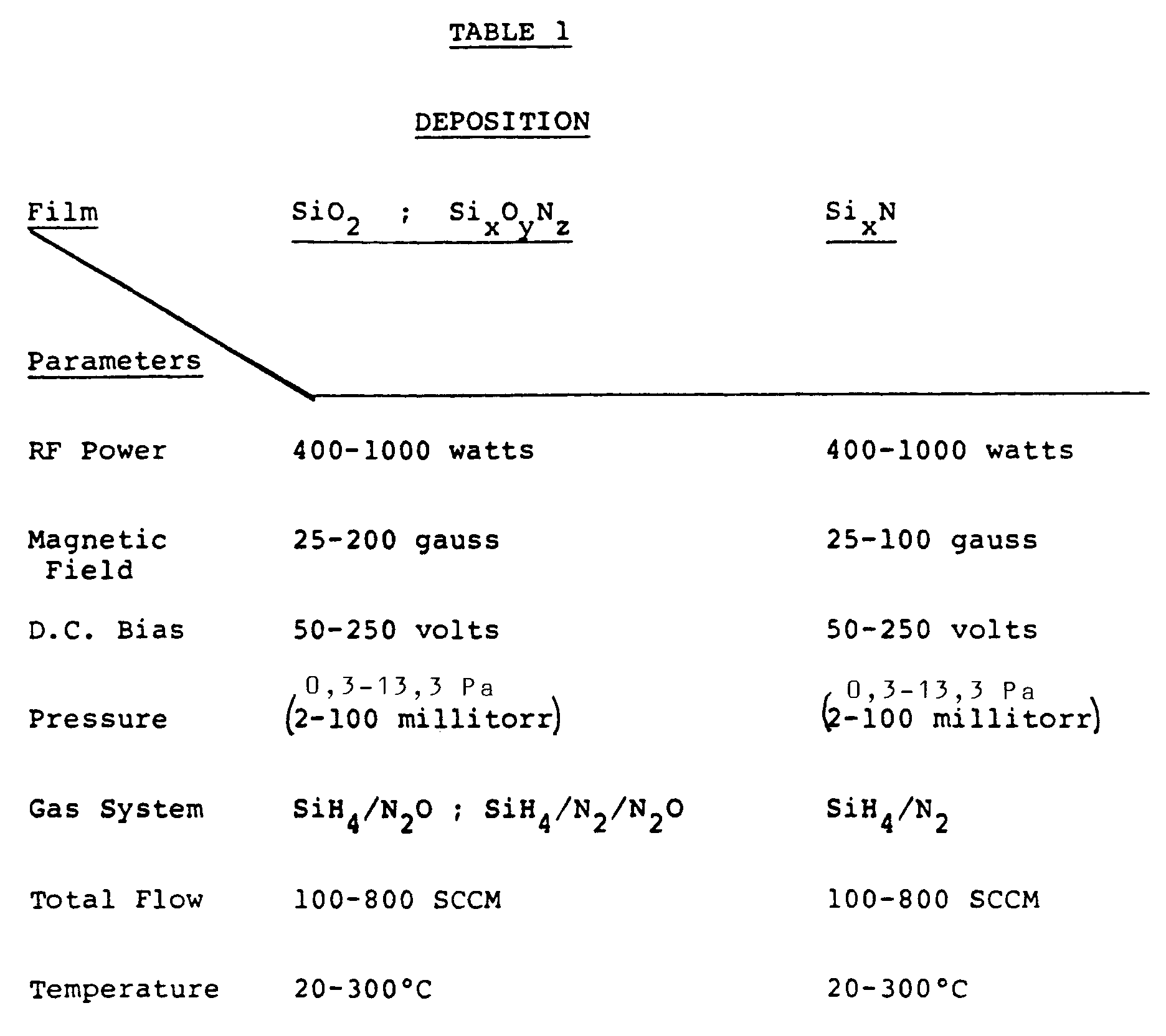
- An experimental program was set up to demonstrate the deposition process. Silicon nitride (SixNy), silicon oxynitride (SixOyNz) and silicon dioxide (Si02) were deposited on monocrystalline silicon films using the general method described above and the process parameters described in Table 1 below. Two different sized reactor chambers 30 were used, with like results. Both used the Helmholtz magnet configuration. The first chamber was 30,5 cm (12 inches) in diameter by 30,5 cm (12 inches) in height, with magnet dimensions of approximately 30,5 cm (12 inches) inside diameter and 15,25 cm (6 inches) separation. The second chamber 30 measured 45,7 cm (18 inches) in inside diameter by 38,1 cm (15 inches) in height and the associated magnets were approximately 45,7 cm (18 inches) in inside diameter with a separation of approximately 22,9 cm (9 inches).
- As mentioned previously, the silicon nitride films were formed using SiH4/N2, i.e., without ammonia, NH3. The silicon oxynitride and silicon dioxide films were formed using SiH4/N2/N20 and SiH4/N20, respectively. Equal N2 and N20 flow rates were used in the oxynitride deposition, but those of ordinary skill in the art understand that the N2/N20 flow rate ratio can be varied to control the oxynitride composition.
- The films were characterized as follows: An indication of the stoichometry of the films was obtained by measuring the refractive index (Nf) using an Ellipsometer. Film thickness was determined using four-point probe measurements. Film thickness values were then used with the deposition times to obtain the deposition rates. The amount of film stress was determined by measuring the net radius of curvature of the wafer after deposition. The films were also wet-etched in buffered hydrogen fluoride (BHF) etching solution (13:2 NH4:HF) at 25 ° C to provide an indirect estimate of film density and quality. A relatively low BHF etch rate of, respectively, up to about 5/90 nm per minute (50/900 Angstroms per minute) for silicon nitride/silicon dioxide is generally considered to be indicative of a high quality, dense film.
- Referring to Table 2, for the deposited silicon nitride, silicon oxynitride, and silicon dioxide films, the measured refractive indices and film composition values were well within the acceptable range.
- Nuclear reaction analysis and IR analysis also indicated a low hydrogen content of 5-13% for the silicon nitride films. In addition, the BHF etch rate of 2-7 nm per minute (20 to 70 Angstroms per minute) is consistent with the 5 nm per minute (50 Angstroms per minute) value which is representative of dense high quality silicon nitride films. The 2-7 nm per minute (20-70 Angstroms per minute) etch rate is taken as evidence that the deposited silicon nitride films were of very high quality and density. Furthermore, the adhesion of the silicon nitride films was excellent. The silicon nitride film compressive stress was about 5 x 10⁹ - 1 x 10¹⁰ dynes per square centimeter. This value is believed characteristic of the high density, high adhesion, low hydrogen content of the silicon nitride films. Finally, the deposition experiments indicated good quality silicon nitride films can be deposited at room temperature by increasing the power to compensate for the lack of supplemental heating. Below about 100°C, high quality films were obtained for pressures 4 4 Pa (30 mtorr) for power levels 400 watts. Also, above about 100°C, the high film quality was insensitive to temperature over the range of process variables.

- For the silicon oxynitride films, the etch rate of 40 nm per minute (400 Angstroms per minute) is again relatively low compared to the values of perhaps 100-250 nm per minute (1,000 - 2,500 Angstroms per minute), depending upon the oxygen content, which are associated with dense films, again suggesting the films were of high quality and were dense. Deposition rates were 100-500 nm per minute (1,000 - 5,000 Angstroms per minute). Hydrogen content was low, about 3-8%, and adhesion was excellent. The films did not exhibit cracking or wrinkling.
- Finally, the deposited silicon dioxide films exhibited an etch rate of about (1,040 to 1,140 Angstroms per minute), indicating a good quality dense film. It is worth noting that the BHF etch rate for quality thermal silicon oxide films (which are formed slowly and require that the IC structure be subjected to relatively high temperatures of about 800 to 900 ° C for long periods of time) is about 900 Angstroms per minute. The thermal oxide-quality of the present, magnetron-enhanced plasma oxide films is provided at low temperatures and extremely short deposition times (because of the very high deposition rate of approximately 100-500 nm per minute (1,000 to 5,000 Angstroms per minute)). In consequence, the existing IC structure is not subjected to high temperature for long periods of time, as is the case with the formation thermal silicon oxide films.
- Furthermore, for silicon oxide films the films were in compression. The compressive stress values were within the range (4.5 - 7.5) 109 dynes per square centimeter, and in general there was no film cracking or wrinkling.
- It should be noted that some film cracking was observed where process pressures were below approximately 0,7 Pa (5 millitorr) and there was evidence of gas phase reaction at about 7 Pa (50 millitorr). The former problem can be avoided by adjustment of the magnetic field whereas the latter is a function of the chamber configuration, power and flow rate.
- It should be noted that the range of deposition rates of about 100-500 nm per minute (1,000 - 5,000 Angstroms per minute) for the nitride, oxynitride and oxide films was a function of magnetic field intensity and gas flow rate, with the higher deposition rates being provided by the higher magnetic field values and/or gas flow rates. Furthermore, the investigations conducted to date indicate the 500 nm (5,000 Angstrom) maximum value is not the upper limit. The experimental data suggests that increasing the magnetic field, or increasing gas flow at a given pressure will provide even higher deposition rates of quality films.
- As mentioned above, the ability to form conformal and planarized films on small dimension dense topographical features, is very important to current and future IC deposition technology. An experimental program was established to investigate the conformal and planarization qualities of magnetron-enhanced plasma silicon nitride and silicon dioxide films. Referring to FIG. 12, the oxide and nitride films 122 were formed to a thickness of one /1.m (micron) on stepped silicon conductor films 121 which were formed with line widths of 0.5-2 microns and step heights of one micron and were separated by 1.5-2 micron-wide trenches. The reactor 30 was used in accordance with the method described above. The TABLE 1 deposition parameters were used to deposit the silicon nitride and silicon oxide films. In addition, silicon oxide films were formed by adding NF3 or CF4 etching gas to the chamber simultaneously with the deposition gas. Both etching and deposition proceed more slowly on the bottom walls 123 and sidewalls 124. Consequently, etching simultaneously with deposition was used to enhance conformal film formation, i.e., to control the step coverage profile by offsetting any differences in deposition rates on the different surfaces and, thus, equalizing film thickness on the bottom 123, sidewalls 124 and top surfaces 125. It was also used to control the deposition rate.
- The step coverage was characterized using SEM (scanning electron micrographs). As shown by the FIG. 12 schematized illustration of the resulting deposited silicon nitride and silicon oxide films 122, the step coverage was quite conformal for both film types (1) and (2). Early in the two-micron growth process, the film thickness at the bottom 123, sidewalls 124 and top surfaces 125 was equal, as indicated by the dotted line 126. The bottom surface cusps and voids associated with conventional plasma deposited films were absent. In short, despite the close step spacing, conformal silicon nitride and silicon dioxide films were obtained. Then, as film deposition continued, a nearly flat, planar upper surface 127 was formed.
- The observed uniform film thickness is thought to be the result of high surface mobility. Please note, the peak-to-peak voltage and the DC bias for given conditions are typically less using a magnetic field than for a zero magnetic field and in consequence the average energy of ions impinging on the substrate 5 (along with substrate and film defect densities) is also lower. Nonetheless, the very high number density of active chemical species arriving at the substrate surface is believed to result in a high surface mobility which provides a uniform film growth. Conformal step coverage is also aided, that is the tendency to form uniform a film of uniform thickness over the top, bottom and sides of steps is increased, as the pressure is decreased, down to a value of at least about 5 millitorr. Variation of the pressure provides control of the profile of the deposited film by in-situ physical sputtering of the film. The mean free path of species arriving at the substrate surface varies with pressure and becomes more unidirectional at low pressure, reducing the film thickness on the edge and top of step coverage due to in-situ physical sputtering.
- In addition to the use of various parameters as discussed above to control film growth rate, conformal coverage and various film characteristics, film stress can be controlled by varying the magnetic field. The effect of magnetic field variation on stress in nitride films was investigated. Low frequency fields (about 50-450 kilohertz) provided higher film stress than did higher frequency fields (about 13-27 megahertz), typically with enhanced adhesion. Low stress, good adhesion nitride films were provided by starting deposition using a low frequency magnetic field, then switching to a high frequency magnetic field. The initial deposition at low frequency provides excellent adhesion to the underlying material, while the stress is a weighted average
Claims (1)
Priority Applications (1)
| Application Number | Priority Date | Filing Date | Title |
|---|---|---|---|
| EP94104745A EP0612861A1 (en) | 1984-10-25 | 1985-10-24 | Apparatus and method for magnetron-enhanced plasma-assisted chemical vapor deposition |
Applications Claiming Priority (2)
| Application Number | Priority Date | Filing Date | Title |
|---|---|---|---|
| US664657 | 1984-10-25 | ||
| US06/664,657 US4668365A (en) | 1984-10-25 | 1984-10-25 | Apparatus and method for magnetron-enhanced plasma-assisted chemical vapor deposition |
Related Child Applications (1)
| Application Number | Title | Priority Date | Filing Date |
|---|---|---|---|
| EP94104745.8 Division-Into | 1994-03-24 |
Publications (3)
| Publication Number | Publication Date |
|---|---|
| EP0179665A2 EP0179665A2 (en) | 1986-04-30 |
| EP0179665A3 EP0179665A3 (en) | 1989-02-08 |
| EP0179665B1 true EP0179665B1 (en) | 1994-12-28 |
Family
ID=24666897
Family Applications (2)
| Application Number | Title | Priority Date | Filing Date |
|---|---|---|---|
| EP85307699A Expired - Lifetime EP0179665B1 (en) | 1984-10-25 | 1985-10-24 | Apparatus and method for magnetron-enhanced plasma-assisted chemical vapor deposition |
| EP94104745A Withdrawn EP0612861A1 (en) | 1984-10-25 | 1985-10-24 | Apparatus and method for magnetron-enhanced plasma-assisted chemical vapor deposition |
Family Applications After (1)
| Application Number | Title | Priority Date | Filing Date |
|---|---|---|---|
| EP94104745A Withdrawn EP0612861A1 (en) | 1984-10-25 | 1985-10-24 | Apparatus and method for magnetron-enhanced plasma-assisted chemical vapor deposition |
Country Status (4)
| Country | Link |
|---|---|
| US (1) | US4668365A (en) |
| EP (2) | EP0179665B1 (en) |
| JP (2) | JPH0696768B2 (en) |
| DE (1) | DE3587964T2 (en) |
Families Citing this family (144)
| Publication number | Priority date | Publication date | Assignee | Title |
|---|---|---|---|---|
| US5780313A (en) | 1985-02-14 | 1998-07-14 | Semiconductor Energy Laboratory Co., Ltd. | Method of fabricating semiconductor device |
| US6784033B1 (en) | 1984-02-15 | 2004-08-31 | Semiconductor Energy Laboratory Co., Ltd. | Method for the manufacture of an insulated gate field effect semiconductor device |
| JPH0752718B2 (en) * | 1984-11-26 | 1995-06-05 | 株式会社半導体エネルギー研究所 | Thin film formation method |
| US6786997B1 (en) | 1984-11-26 | 2004-09-07 | Semiconductor Energy Laboratory Co., Ltd. | Plasma processing apparatus |
| US4797527A (en) * | 1985-02-06 | 1989-01-10 | Kanegafuchi Kagaku Kogyo Kabushiki Kaisha | Electrode for electric discharge machining and method for producing the same |
| US6673722B1 (en) | 1985-10-14 | 2004-01-06 | Semiconductor Energy Laboratory Co., Ltd. | Microwave enhanced CVD system under magnetic field |
| US5512102A (en) * | 1985-10-14 | 1996-04-30 | Semiconductor Energy Laboratory Co., Ltd. | Microwave enhanced CVD system under magnetic field |
| US6230650B1 (en) | 1985-10-14 | 2001-05-15 | Semiconductor Energy Laboratory Co., Ltd. | Microwave enhanced CVD system under magnetic field |
| US4949671A (en) * | 1985-10-24 | 1990-08-21 | Texas Instruments Incorporated | Processing apparatus and method |
| US5300951A (en) * | 1985-11-28 | 1994-04-05 | Kabushiki Kaisha Toshiba | Member coated with ceramic material and method of manufacturing the same |
| US5366554A (en) * | 1986-01-14 | 1994-11-22 | Canon Kabushiki Kaisha | Device for forming a deposited film |
| US4974543A (en) * | 1986-02-28 | 1990-12-04 | Xerox Corporation | Apparatus for amorphous silicon film |
| US4873605A (en) * | 1986-03-03 | 1989-10-10 | Innovex, Inc. | Magnetic treatment of ferromagnetic materials |
| US4786361A (en) * | 1986-03-05 | 1988-11-22 | Kabushiki Kaisha Toshiba | Dry etching process |
| US5308431A (en) * | 1986-04-18 | 1994-05-03 | General Signal Corporation | System providing multiple processing of substrates |
| US5102495A (en) * | 1986-04-18 | 1992-04-07 | General Signal Corporation | Method providing multiple-processing of substrates |
| CA1331163C (en) * | 1986-04-18 | 1994-08-02 | Applied Materials, Inc. | Multiple-processing and contamination-free plasma etching system |
| US6103055A (en) * | 1986-04-18 | 2000-08-15 | Applied Materials, Inc. | System for processing substrates |
| US5013385A (en) * | 1986-04-18 | 1991-05-07 | General Signal Corporation | Quad processor |
| US5044314A (en) * | 1986-10-15 | 1991-09-03 | Advantage Production Technology, Inc. | Semiconductor wafer processing apparatus |
| GB8629634D0 (en) * | 1986-12-11 | 1987-01-21 | Dobson C D | Reactive ion & sputter etching |
| US5215619A (en) * | 1986-12-19 | 1993-06-01 | Applied Materials, Inc. | Magnetic field-enhanced plasma etch reactor |
| ATE177877T1 (en) * | 1986-12-19 | 1999-04-15 | Applied Materials Inc | BROMINE ETCHING PROCESS FOR SILICON |
| US5277939A (en) * | 1987-02-10 | 1994-01-11 | Semiconductor Energy Laboratory Co., Ltd. | ECR CVD method for forming BN films |
| US4793897A (en) * | 1987-03-20 | 1988-12-27 | Applied Materials, Inc. | Selective thin film etch process |
| JPS63244619A (en) * | 1987-03-30 | 1988-10-12 | Sumitomo Metal Ind Ltd | Plasma system |
| FR2614317B1 (en) * | 1987-04-22 | 1989-07-13 | Air Liquide | PROCESS FOR PROTECTING POLYMERIC SUBSTRATE BY PLASMA DEPOSITION OF COMPOUNDS OF THE SILICON OXYNITRIDE TYPE AND DEVICE FOR IMPLEMENTING SAME. |
| US4912065A (en) * | 1987-05-28 | 1990-03-27 | Matsushita Electric Industrial Co., Ltd. | Plasma doping method |
| DE3719616A1 (en) * | 1987-06-12 | 1988-12-29 | Leybold Ag | METHOD AND DEVICE FOR COATING A SUBSTRATE |
| ZA884511B (en) * | 1987-07-15 | 1989-03-29 | Boc Group Inc | Method of plasma enhanced silicon oxide deposition |
| US4854263B1 (en) * | 1987-08-14 | 1997-06-17 | Applied Materials Inc | Inlet manifold and methods for increasing gas dissociation and for PECVD of dielectric films |
| KR910007384B1 (en) * | 1987-09-16 | 1991-09-25 | 가부시끼가이샤 한도다이 에네르기 겐뀨쇼 | Formation of superconductor oxide film |
| US4991542A (en) * | 1987-10-14 | 1991-02-12 | The Furukawa Electric Co., Ltd. | Method of forming a thin film by plasma CVD and apapratus for forming a thin film |
| JP2512783B2 (en) * | 1988-04-20 | 1996-07-03 | 株式会社日立製作所 | Plasma etching method and apparatus |
| FR2631346B1 (en) * | 1988-05-11 | 1994-05-20 | Air Liquide | MULTILAYER PROTECTIVE COATING FOR SUBSTRATE, METHOD FOR PROTECTING SUBSTRATE BY PLASMA DEPOSITION OF SUCH A COATING, COATINGS OBTAINED AND APPLICATIONS THEREOF |
| JPH0223613A (en) * | 1988-07-12 | 1990-01-25 | Tokyo Ohka Kogyo Co Ltd | Plasma reactor |
| WO1990004045A1 (en) * | 1988-10-14 | 1990-04-19 | Advantage Production Technology Inc. | Semiconductor wafer processing method and apparatus |
| US5076205A (en) * | 1989-01-06 | 1991-12-31 | General Signal Corporation | Modular vapor processor system |
| DE3902628A1 (en) * | 1989-01-30 | 1990-08-02 | Hauni Elektronik Gmbh | THICK FILM MATERIAL FOR SENSORS OR ACTUATORS AND METHOD FOR THE PRODUCTION THEREOF |
| US5421891A (en) * | 1989-06-13 | 1995-06-06 | Plasma & Materials Technologies, Inc. | High density plasma deposition and etching apparatus |
| US4948458A (en) * | 1989-08-14 | 1990-08-14 | Lam Research Corporation | Method and apparatus for producing magnetically-coupled planar plasma |
| JPH0784662B2 (en) * | 1989-12-12 | 1995-09-13 | アプライドマテリアルズジャパン株式会社 | Chemical vapor deposition method and apparatus |
| US4971655A (en) * | 1989-12-26 | 1990-11-20 | Micron Technology, Inc. | Protection of a refractory metal silicide during high-temperature processing using a dual-layer cap of silicon dioxide and silicon nitride |
| DE4010672A1 (en) * | 1990-04-03 | 1991-10-10 | Leybold Ag | Reactive ion etching process - useful for rapid anisotropic etching of masked semiconductor substrates |
| US5186594A (en) * | 1990-04-19 | 1993-02-16 | Applied Materials, Inc. | Dual cassette load lock |
| CA2039109A1 (en) * | 1990-04-23 | 1991-10-24 | David B. Chang | Selective emissivity coatings for interior temperature reduction of an enclosure |
| FR2661688B1 (en) * | 1990-05-02 | 1992-07-17 | Air Liquide | MULTILAYER COATING FOR POLYCARBONATE SUBSTRATE AND PROCESS FOR PREPARING SUCH A COATING. |
| US5089442A (en) * | 1990-09-20 | 1992-02-18 | At&T Bell Laboratories | Silicon dioxide deposition method using a magnetic field and both sputter deposition and plasma-enhanced cvd |
| US5274270A (en) * | 1990-12-17 | 1993-12-28 | Nchip, Inc. | Multichip module having SiO2 insulating layer |
| JP3139031B2 (en) * | 1991-02-21 | 2001-02-26 | 日本板硝子株式会社 | Heat shielding glass |
| JP3670277B2 (en) | 1991-05-17 | 2005-07-13 | ラム リサーチ コーポレーション | Method for depositing SiOx films with low intrinsic stress and / or low hydrogen content |
| DE4118973C2 (en) * | 1991-06-08 | 1999-02-04 | Fraunhofer Ges Forschung | Device for the plasma-assisted processing of substrates and use of this device |
| US5212118A (en) * | 1991-08-09 | 1993-05-18 | Saxena Arjun N | Method for selective chemical vapor deposition of dielectric, semiconductor and conductive films on semiconductor and metallic substrates |
| US5204138A (en) * | 1991-12-24 | 1993-04-20 | International Business Machines Corporation | Plasma enhanced CVD process for fluorinated silicon nitride films |
| JP2791525B2 (en) * | 1992-04-16 | 1998-08-27 | 三菱電機株式会社 | Method of selecting antireflection film and antireflection film selected by the method |
| US5277751A (en) * | 1992-06-18 | 1994-01-11 | Ogle John S | Method and apparatus for producing low pressure planar plasma using a coil with its axis parallel to the surface of a coupling window |
| US5248371A (en) * | 1992-08-13 | 1993-09-28 | General Signal Corporation | Hollow-anode glow discharge apparatus |
| EP0602595B1 (en) * | 1992-12-15 | 1997-07-23 | Applied Materials, Inc. | Vaporizing reactant liquids for CVD |
| JP2875945B2 (en) * | 1993-01-28 | 1999-03-31 | アプライド マテリアルズ インコーポレイテッド | Method of depositing silicon nitride thin film on large area glass substrate at high deposition rate by CVD |
| US5542559A (en) * | 1993-02-16 | 1996-08-06 | Tokyo Electron Kabushiki Kaisha | Plasma treatment apparatus |
| JPH06326026A (en) | 1993-04-13 | 1994-11-25 | Applied Materials Inc | Formation method for thin film in semiconductor device |
| CH687987A5 (en) * | 1993-05-03 | 1997-04-15 | Balzers Hochvakuum | A process for the increase of the deposition rate in a plasma discharge space and plasma chamber. |
| US5571571A (en) * | 1993-06-16 | 1996-11-05 | Applied Materials, Inc. | Method of forming a thin film for a semiconductor device |
| US5851602A (en) * | 1993-12-09 | 1998-12-22 | Applied Materials, Inc. | Deposition of high quality conformal silicon oxide thin films for the manufacture of thin film transistors |
| EP0661732B1 (en) | 1993-12-28 | 2004-06-09 | Applied Materials, Inc. | A method of forming silicon oxy-nitride films by plasma-enhanced chemical vapor deposition |
| JP3080843B2 (en) * | 1994-08-24 | 2000-08-28 | 松下電器産業株式会社 | Thin film forming method and apparatus |
| EP0723944A1 (en) * | 1995-01-26 | 1996-07-31 | Optical Coating Laboratory, Inc. | Wear resistant windows |
| JPH08203884A (en) * | 1995-01-31 | 1996-08-09 | Mitsubishi Electric Corp | Oxynitride, deposition thereof, and deposition of isolation oxide of oxynitride |
| US5571576A (en) * | 1995-02-10 | 1996-11-05 | Watkins-Johnson | Method of forming a fluorinated silicon oxide layer using plasma chemical vapor deposition |
| US5962923A (en) * | 1995-08-07 | 1999-10-05 | Applied Materials, Inc. | Semiconductor device having a low thermal budget metal filling and planarization of contacts, vias and trenches |
| US6238533B1 (en) | 1995-08-07 | 2001-05-29 | Applied Materials, Inc. | Integrated PVD system for aluminum hole filling using ionized metal adhesion layer |
| JP3979687B2 (en) | 1995-10-26 | 2007-09-19 | アプライド マテリアルズ インコーポレイテッド | Method for improving film stability of halogen-doped silicon oxide films |
| US6144544A (en) * | 1996-10-01 | 2000-11-07 | Milov; Vladimir N. | Apparatus and method for material treatment using a magnetic field |
| US6113731A (en) * | 1997-01-02 | 2000-09-05 | Applied Materials, Inc. | Magnetically-enhanced plasma chamber with non-uniform magnetic field |
| JP3343200B2 (en) * | 1997-05-20 | 2002-11-11 | 東京エレクトロン株式会社 | Plasma processing equipment |
| US20050272254A1 (en) * | 1997-11-26 | 2005-12-08 | Applied Materials, Inc. | Method of depositing low resistivity barrier layers for copper interconnects |
| JP4947834B2 (en) * | 1997-11-26 | 2012-06-06 | アプライド マテリアルズ インコーポレイテッド | Damage-free coating engraving deposition method |
| US7253109B2 (en) * | 1997-11-26 | 2007-08-07 | Applied Materials, Inc. | Method of depositing a tantalum nitride/tantalum diffusion barrier layer system |
| US6015476A (en) * | 1998-02-05 | 2000-01-18 | Applied Materials, Inc. | Plasma reactor magnet with independently controllable parallel axial current-carrying elements |
| US7378146B1 (en) * | 1998-08-05 | 2008-05-27 | International Business Machines Corporation | Transparent hard coats for optical elements |
| US6328858B1 (en) | 1998-10-01 | 2001-12-11 | Nexx Systems Packaging, Llc | Multi-layer sputter deposition apparatus |
| US6217272B1 (en) | 1998-10-01 | 2001-04-17 | Applied Science And Technology, Inc. | In-line sputter deposition system |
| US6579421B1 (en) | 1999-01-07 | 2003-06-17 | Applied Materials, Inc. | Transverse magnetic field for ionized sputter deposition |
| TW455912B (en) * | 1999-01-22 | 2001-09-21 | Sony Corp | Method and apparatus for film deposition |
| US6251776B1 (en) * | 1999-04-02 | 2001-06-26 | Advanced Micro Devices, Inc. | Plasma treatment to reduce stress corrosion induced voiding of patterned metal layers |
| JP4393677B2 (en) | 1999-09-14 | 2010-01-06 | 株式会社堀場エステック | Liquid material vaporization method and apparatus, and control valve |
| US6372668B2 (en) * | 2000-01-18 | 2002-04-16 | Advanced Micro Devices, Inc. | Method of forming silicon oxynitride films |
| US20070048882A1 (en) * | 2000-03-17 | 2007-03-01 | Applied Materials, Inc. | Method to reduce plasma-induced charging damage |
| US8048806B2 (en) * | 2000-03-17 | 2011-11-01 | Applied Materials, Inc. | Methods to avoid unstable plasma states during a process transition |
| US8617351B2 (en) * | 2002-07-09 | 2013-12-31 | Applied Materials, Inc. | Plasma reactor with minimal D.C. coils for cusp, solenoid and mirror fields for plasma uniformity and device damage reduction |
| US6821912B2 (en) | 2000-07-27 | 2004-11-23 | Nexx Systems Packaging, Llc | Substrate processing pallet and related substrate processing method and machine |
| US6530733B2 (en) | 2000-07-27 | 2003-03-11 | Nexx Systems Packaging, Llc | Substrate processing pallet and related substrate processing method and machine |
| US6682288B2 (en) | 2000-07-27 | 2004-01-27 | Nexx Systems Packaging, Llc | Substrate processing pallet and related substrate processing method and machine |
| US20020197402A1 (en) * | 2000-12-06 | 2002-12-26 | Chiang Tony P. | System for depositing a film by modulated ion-induced atomic layer deposition (MII-ALD) |
| JP4009087B2 (en) * | 2001-07-06 | 2007-11-14 | アプライド マテリアルズ インコーポレイテッド | Magnetic generator in semiconductor manufacturing apparatus, semiconductor manufacturing apparatus, and magnetic field intensity control method |
| US7374636B2 (en) * | 2001-07-06 | 2008-05-20 | Applied Materials, Inc. | Method and apparatus for providing uniform plasma in a magnetic field enhanced plasma reactor |
| KR20040028985A (en) * | 2001-09-14 | 2004-04-03 | 동경 엘렉트론 주식회사 | Plasma reactor coil magnet system |
| TWI283899B (en) * | 2002-07-09 | 2007-07-11 | Applied Materials Inc | Capacitively coupled plasma reactor with magnetic plasma control |
| WO2004022238A2 (en) * | 2002-09-09 | 2004-03-18 | Oster Magnetics, Inc. | Apparatus for manipulating magnetic fields |
| DE10247051A1 (en) * | 2002-10-09 | 2004-04-22 | Polymer Latex Gmbh & Co Kg | Latex and process for its manufacture |
| US7458335B1 (en) | 2002-10-10 | 2008-12-02 | Applied Materials, Inc. | Uniform magnetically enhanced reactive ion etching using nested electromagnetic coils |
| KR101177127B1 (en) * | 2002-11-29 | 2012-08-24 | 오씨 외를리콘 발처스 악티엔게젤샤프트 | Method for the production of a substrate and unit for the same |
| US7422654B2 (en) * | 2003-02-14 | 2008-09-09 | Applied Materials, Inc. | Method and apparatus for shaping a magnetic field in a magnetic field-enhanced plasma reactor |
| US7100954B2 (en) * | 2003-07-11 | 2006-09-05 | Nexx Systems, Inc. | Ultra-thin wafer handling system |
| US8470141B1 (en) * | 2005-04-29 | 2013-06-25 | Angstrom Sciences, Inc. | High power cathode |
| US7967911B2 (en) | 2006-04-11 | 2011-06-28 | Applied Materials, Inc. | Apparatus and methods for chemical vapor deposition |
| WO2007139140A1 (en) | 2006-05-31 | 2007-12-06 | Tokyo Electron Limited | Plasma cvd method, method for forming silicon nitride film and method for manufacturing semiconductor device |
| JP2008071982A (en) * | 2006-09-15 | 2008-03-27 | Hitachi Industrial Equipment Systems Co Ltd | Transformer |
| US7496423B2 (en) * | 2007-05-11 | 2009-02-24 | Applied Materials, Inc. | Method of achieving high productivity fault tolerant photovoltaic factory with batch array transfer robots |
| US20080279672A1 (en) * | 2007-05-11 | 2008-11-13 | Bachrach Robert Z | Batch equipment robots and methods of stack to array work-piece transfer for photovoltaic factory |
| US20080279658A1 (en) * | 2007-05-11 | 2008-11-13 | Bachrach Robert Z | Batch equipment robots and methods within equipment work-piece transfer for photovoltaic factory |
| US20080292433A1 (en) * | 2007-05-11 | 2008-11-27 | Bachrach Robert Z | Batch equipment robots and methods of array to array work-piece transfer for photovoltaic factory |
| US8366997B2 (en) | 2009-02-10 | 2013-02-05 | Shoto Technologies Llc | Modular laboratory automation system |
| EP3222749A1 (en) | 2009-05-13 | 2017-09-27 | SiO2 Medical Products, Inc. | Outgassing method for inspecting a coated surface |
| WO2013170052A1 (en) | 2012-05-09 | 2013-11-14 | Sio2 Medical Products, Inc. | Saccharide protective coating for pharmaceutical package |
| US9458536B2 (en) | 2009-07-02 | 2016-10-04 | Sio2 Medical Products, Inc. | PECVD coating methods for capped syringes, cartridges and other articles |
| US11624115B2 (en) | 2010-05-12 | 2023-04-11 | Sio2 Medical Products, Inc. | Syringe with PECVD lubrication |
| KR20130057460A (en) * | 2010-08-31 | 2013-05-31 | 시마쯔 코포레이션 | Amorphous silicon nitride film and method for producing same |
| JP5594773B2 (en) * | 2010-09-30 | 2014-09-24 | 国立大学法人九州大学 | Selective film formation method, film formation apparatus, and structure |
| US9878101B2 (en) | 2010-11-12 | 2018-01-30 | Sio2 Medical Products, Inc. | Cyclic olefin polymer vessels and vessel coating methods |
| US8697198B2 (en) * | 2011-03-31 | 2014-04-15 | Veeco Ald Inc. | Magnetic field assisted deposition |
| US9272095B2 (en) | 2011-04-01 | 2016-03-01 | Sio2 Medical Products, Inc. | Vessels, contact surfaces, and coating and inspection apparatus and methods |
| US11116695B2 (en) | 2011-11-11 | 2021-09-14 | Sio2 Medical Products, Inc. | Blood sample collection tube |
| EP2776603B1 (en) | 2011-11-11 | 2019-03-06 | SiO2 Medical Products, Inc. | PASSIVATION, pH PROTECTIVE OR LUBRICITY COATING FOR PHARMACEUTICAL PACKAGE, COATING PROCESS AND APPARATUS |
| US9554968B2 (en) | 2013-03-11 | 2017-01-31 | Sio2 Medical Products, Inc. | Trilayer coated pharmaceutical packaging |
| CA2890066C (en) | 2012-11-01 | 2021-11-09 | Sio2 Medical Products, Inc. | Coating inspection method |
| EP2920567B1 (en) | 2012-11-16 | 2020-08-19 | SiO2 Medical Products, Inc. | Method and apparatus for detecting rapid barrier coating integrity characteristics |
| EP2738790A1 (en) * | 2012-11-28 | 2014-06-04 | Abengoa Solar New Technologies, S.A. | Procedure for preparing one single barrier and/or dielectric layer or multilayer on a substrate and device for the implementation thereof |
| US9764093B2 (en) * | 2012-11-30 | 2017-09-19 | Sio2 Medical Products, Inc. | Controlling the uniformity of PECVD deposition |
| CN105705676B (en) * | 2012-11-30 | 2018-09-07 | Sio2医药产品公司 | Control the uniformity of the PECVD depositions on injector for medical purpose, cylindrantherae etc. |
| US20160015898A1 (en) | 2013-03-01 | 2016-01-21 | Sio2 Medical Products, Inc. | Plasma or cvd pre-treatment for lubricated pharmaceutical package, coating process and apparatus |
| US9937099B2 (en) | 2013-03-11 | 2018-04-10 | Sio2 Medical Products, Inc. | Trilayer coated pharmaceutical packaging with low oxygen transmission rate |
| US9564309B2 (en) * | 2013-03-14 | 2017-02-07 | Asm Ip Holding B.V. | Si precursors for deposition of SiN at low temperatures |
| US9824881B2 (en) | 2013-03-14 | 2017-11-21 | Asm Ip Holding B.V. | Si precursors for deposition of SiN at low temperatures |
| US9863042B2 (en) | 2013-03-15 | 2018-01-09 | Sio2 Medical Products, Inc. | PECVD lubricity vessel coating, coating process and apparatus providing different power levels in two phases |
| EP3122917B1 (en) | 2014-03-28 | 2020-05-06 | SiO2 Medical Products, Inc. | Antistatic coatings for plastic vessels |
| US10151025B2 (en) * | 2014-07-31 | 2018-12-11 | Seagate Technology Llc | Helmholtz coil assisted PECVD carbon source |
| US9576792B2 (en) | 2014-09-17 | 2017-02-21 | Asm Ip Holding B.V. | Deposition of SiN |
| WO2017031354A2 (en) | 2015-08-18 | 2017-02-23 | Sio2 Medical Products, Inc. | Pharmaceutical and other packaging with low oxygen transmission rate |
| US10410857B2 (en) | 2015-08-24 | 2019-09-10 | Asm Ip Holding B.V. | Formation of SiN thin films |
| US10006123B2 (en) * | 2016-05-10 | 2018-06-26 | The Boeing Company | Species controlled chemical vapor deposition |
| US10580645B2 (en) | 2018-04-30 | 2020-03-03 | Asm Ip Holding B.V. | Plasma enhanced atomic layer deposition (PEALD) of SiN using silicon-hydrohalide precursors |
| TWI686106B (en) * | 2019-01-25 | 2020-02-21 | 國立清華大學 | Field emission enhanced handheld atmospheric pressure plasma generator |
| CN113496869A (en) * | 2020-04-03 | 2021-10-12 | 重庆超硅半导体有限公司 | Back film layer of silicon wafer for epitaxial substrate and manufacturing method thereof |
Family Cites Families (17)
| Publication number | Priority date | Publication date | Assignee | Title |
|---|---|---|---|---|
| US3558348A (en) * | 1968-04-18 | 1971-01-26 | Bell Telephone Labor Inc | Dielectric films for semiconductor devices |
| US4155825A (en) * | 1977-05-02 | 1979-05-22 | Fournier Paul R | Integrated sputtering apparatus and method |
| GB2009249B (en) * | 1977-11-24 | 1982-06-30 | Lysaght Australia Ltd | Coating mass controll using magnetic field |
| US4265729A (en) * | 1978-09-27 | 1981-05-05 | Vac-Tec Systems, Inc. | Magnetically enhanced sputtering device |
| DE2941559C2 (en) * | 1979-10-13 | 1983-03-03 | Messerschmitt-Bölkow-Blohm GmbH, 8000 München | Process for depositing silicon on a substrate |
| US4361472A (en) * | 1980-09-15 | 1982-11-30 | Vac-Tec Systems, Inc. | Sputtering method and apparatus utilizing improved ion source |
| JPS5756036A (en) * | 1980-09-20 | 1982-04-03 | Mitsubishi Electric Corp | Plasma chemical vapor phase reactor |
| US4487162A (en) * | 1980-11-25 | 1984-12-11 | Cann Gordon L | Magnetoplasmadynamic apparatus for the separation and deposition of materials |
| JPS57161057A (en) * | 1981-03-30 | 1982-10-04 | Mitsubishi Electric Corp | Chemical vapor phase growth device using plasma |
| DE3280026D1 (en) * | 1981-05-29 | 1989-12-21 | Kanegafuchi Chemical Ind | Process for preparing amorphous silicon semiconductor |
| US4512283A (en) * | 1982-02-01 | 1985-04-23 | Texas Instruments Incorporated | Plasma reactor sidewall shield |
| IN160089B (en) * | 1982-07-14 | 1987-06-27 | Standard Oil Co Ohio | |
| JPS5944831A (en) * | 1982-09-07 | 1984-03-13 | Toshiba Corp | Deposition of thin film |
| US4500409A (en) * | 1983-07-19 | 1985-02-19 | Varian Associates, Inc. | Magnetron sputter coating source for both magnetic and non magnetic target materials |
| US4500408A (en) * | 1983-07-19 | 1985-02-19 | Varian Associates, Inc. | Apparatus for and method of controlling sputter coating |
| JPS60200956A (en) * | 1984-03-23 | 1985-10-11 | Anelva Corp | Discharge reaction device |
| JPS619577U (en) * | 1984-06-23 | 1986-01-21 | ダイキン工業株式会社 | Scroll type fluid machine |
-
1984
- 1984-10-25 US US06/664,657 patent/US4668365A/en not_active Expired - Fee Related
-
1985
- 1985-10-24 EP EP85307699A patent/EP0179665B1/en not_active Expired - Lifetime
- 1985-10-24 DE DE3587964T patent/DE3587964T2/en not_active Expired - Fee Related
- 1985-10-24 EP EP94104745A patent/EP0612861A1/en not_active Withdrawn
- 1985-10-25 JP JP60239253A patent/JPH0696768B2/en not_active Expired - Lifetime
-
1994
- 1994-06-29 JP JP6147307A patent/JPH07166360A/en active Pending
Non-Patent Citations (1)
| Title |
|---|
| APPLIED PHYSICS LETTERS, vol. 37, no. 9, November 01, 1980, pp. 787-788, American Institute of Physics, New York, NY, US; M.TANIGUCHI et al.: "Novel effects of magnetic field on the silane glow discharge" * |
Also Published As
| Publication number | Publication date |
|---|---|
| EP0612861A1 (en) | 1994-08-31 |
| DE3587964T2 (en) | 1995-05-11 |
| JPS61179872A (en) | 1986-08-12 |
| EP0179665A3 (en) | 1989-02-08 |
| JPH0696768B2 (en) | 1994-11-30 |
| EP0179665A2 (en) | 1986-04-30 |
| US4668365A (en) | 1987-05-26 |
| DE3587964D1 (en) | 1995-02-09 |
| JPH07166360A (en) | 1995-06-27 |
Similar Documents
| Publication | Publication Date | Title |
|---|---|---|
| EP0179665B1 (en) | Apparatus and method for magnetron-enhanced plasma-assisted chemical vapor deposition | |
| US4668338A (en) | Magnetron-enhanced plasma etching process | |
| US6444084B1 (en) | Low density high frequency process for a parallel-plate electrode plasma reactor having an inductive antenna | |
| US6191026B1 (en) | Method for submicron gap filling on a semiconductor substrate | |
| US7138767B2 (en) | Surface wave plasma processing system and method of using | |
| US7268084B2 (en) | Method for treating a substrate | |
| US7396431B2 (en) | Plasma processing system for treating a substrate | |
| US5770098A (en) | Etching process | |
| KR100355914B1 (en) | Direct Circuit Manufacturing Method Using Low Temperature Plasma | |
| US6291357B1 (en) | Method and apparatus for etching a substrate with reduced microloading | |
| KR100849707B1 (en) | Selective etching of carbon-doped low-k dielectrics | |
| US6583065B1 (en) | Sidewall polymer forming gas additives for etching processes | |
| US20060029745A1 (en) | High throughput ILD fill process for high aspect ratio gap fill | |
| JPH0740569B2 (en) | ECR plasma deposition method | |
| JPH05308062A (en) | Dry etching method | |
| US5880033A (en) | Method for etching metal silicide with high selectivity to polysilicon | |
| JPH08236513A (en) | Method of etching substrate in plasma | |
| US7584714B2 (en) | Method and system for improving coupling between a surface wave plasma source and a plasma space | |
| JPH09312297A (en) | Plasma annealing of thin film | |
| US20030235993A1 (en) | Selective etching of low-k dielectrics | |
| JPH11168090A (en) | Semiconductor manufacturing method | |
| EP0469791A1 (en) | Soluble oxides for integrated circuits | |
| US6492279B1 (en) | Plasma etching methods | |
| JP3220528B2 (en) | Vacuum processing equipment | |
| Matsuo | Reactive ion-beam etching and plasma deposition techniques using electron cyclotron resonance plasmas |
Legal Events
| Date | Code | Title | Description |
|---|---|---|---|
| PUAI | Public reference made under article 153(3) epc to a published international application that has entered the european phase |
Free format text: ORIGINAL CODE: 0009012 |
|
| AK | Designated contracting states |
Kind code of ref document: A2 Designated state(s): CH DE FR GB IT LI NL |
|
| PUAL | Search report despatched |
Free format text: ORIGINAL CODE: 0009013 |
|
| AK | Designated contracting states |
Kind code of ref document: A3 Designated state(s): CH DE FR GB IT LI NL |
|
| 17P | Request for examination filed |
Effective date: 19890801 |
|
| 17Q | First examination report despatched |
Effective date: 19900117 |
|
| GRAA | (expected) grant |
Free format text: ORIGINAL CODE: 0009210 |
|
| ITF | It: translation for a ep patent filed |
Owner name: FUMERO BREVETTI S.N.C. |
|
| AK | Designated contracting states |
Kind code of ref document: B1 Designated state(s): CH DE FR GB IT LI NL |
|
| PG25 | Lapsed in a contracting state [announced via postgrant information from national office to epo] |
Ref country code: LI Effective date: 19941228 Ref country code: CH Effective date: 19941228 |
|
| REF | Corresponds to: |
Ref document number: 3587964 Country of ref document: DE Date of ref document: 19950209 |
|
| ET | Fr: translation filed | ||
| REG | Reference to a national code |
Ref country code: CH Ref legal event code: PL |
|
| PGFP | Annual fee paid to national office [announced via postgrant information from national office to epo] |
Ref country code: GB Payment date: 19950825 Year of fee payment: 11 |
|
| PGFP | Annual fee paid to national office [announced via postgrant information from national office to epo] |
Ref country code: FR Payment date: 19950928 Year of fee payment: 11 |
|
| PGFP | Annual fee paid to national office [announced via postgrant information from national office to epo] |
Ref country code: NL Payment date: 19951027 Year of fee payment: 11 |
|
| PLBE | No opposition filed within time limit |
Free format text: ORIGINAL CODE: 0009261 |
|
| STAA | Information on the status of an ep patent application or granted ep patent |
Free format text: STATUS: NO OPPOSITION FILED WITHIN TIME LIMIT |
|
| 26N | No opposition filed | ||
| PGFP | Annual fee paid to national office [announced via postgrant information from national office to epo] |
Ref country code: DE Payment date: 19951229 Year of fee payment: 11 |
|
| PG25 | Lapsed in a contracting state [announced via postgrant information from national office to epo] |
Ref country code: GB Effective date: 19961024 |
|
| PG25 | Lapsed in a contracting state [announced via postgrant information from national office to epo] |
Ref country code: NL Effective date: 19970501 |
|
| GBPC | Gb: european patent ceased through non-payment of renewal fee |
Effective date: 19961024 |
|
| PG25 | Lapsed in a contracting state [announced via postgrant information from national office to epo] |
Ref country code: FR Effective date: 19970630 |
|
| NLV4 | Nl: lapsed or anulled due to non-payment of the annual fee |
Effective date: 19970501 |
|
| PG25 | Lapsed in a contracting state [announced via postgrant information from national office to epo] |
Ref country code: DE Effective date: 19970701 |
|
| REG | Reference to a national code |
Ref country code: FR Ref legal event code: ST |