EP0188134A2 - Semiconductor memory device having serial data input and output circuit - Google Patents
Semiconductor memory device having serial data input and output circuit Download PDFInfo
- Publication number
- EP0188134A2 EP0188134A2 EP85309562A EP85309562A EP0188134A2 EP 0188134 A2 EP0188134 A2 EP 0188134A2 EP 85309562 A EP85309562 A EP 85309562A EP 85309562 A EP85309562 A EP 85309562A EP 0188134 A2 EP0188134 A2 EP 0188134A2
- Authority
- EP
- European Patent Office
- Prior art keywords
- memory device
- semiconductor memory
- serial data
- gates
- serial
- Prior art date
- Legal status (The legal status is an assumption and is not a legal conclusion. Google has not performed a legal analysis and makes no representation as to the accuracy of the status listed.)
- Granted
Links
Images


Classifications
-
- H—ELECTRICITY
- H01—ELECTRIC ELEMENTS
- H01L—SEMICONDUCTOR DEVICES NOT COVERED BY CLASS H10
- H01L27/00—Devices consisting of a plurality of semiconductor or other solid-state components formed in or on a common substrate
-
- G—PHYSICS
- G11—INFORMATION STORAGE
- G11C—STATIC STORES
- G11C7/00—Arrangements for writing information into, or reading information out from, a digital store
- G11C7/10—Input/output [I/O] data interface arrangements, e.g. I/O data control circuits, I/O data buffers
- G11C7/1075—Input/output [I/O] data interface arrangements, e.g. I/O data control circuits, I/O data buffers for multiport memories each having random access ports and serial ports, e.g. video RAM
-
- G—PHYSICS
- G11—INFORMATION STORAGE
- G11C—STATIC STORES
- G11C7/00—Arrangements for writing information into, or reading information out from, a digital store
Definitions
- the present invention relates to a semiconductor memory device. More particularly, it relates to a semiconductor memory device having a high-speed serial data input and output circuit in addition to a random data input and output circuit.
- An image data processing system or the like requires a large-capacity memory.
- a dynamic random-access memory is extensively used.
- high-speed data store and/or read-out are also highly required.
- dual-port memory devices i.e., semiconductor memory devices including a high-speed data input and output circuit provided outside the dynamic RAM.
- a dual-port memory device is operable for not only normal random access through a conventional port, but also high-speed serial data input and output used by a high-speed data input and output circuit through another port.
- a semiconductor memory device including: at least one memory cell array including a plurality of memory cells arranged in a matrix form with a plurality of bit lines and a plurality of word lines, a circuit, operatively connected to the memory cell array, for selecting one of the word lines in response to an address signal, and a plurality of gates, operatively connected between the bit lines and at least one data bus, for transferring data to be stored or read between the bit lines and the data bus.
- the semiconductor memory device also includes a circuit for serially data input and output, including a plurality of transfer gates, operatively connected to the bit lines, and operable in a group in response to a transfer clock pulse, a plurality of latch circuits having terminals operatively connected to the transfer gates and holding data to be stored or read, a plurality of serial gates, having terminals operatively connected to other terminals of the latch circuits and having other terminals connected to at least one serial data bus, and a plurality of ring-connected shift registers triggering the serial gates, a single bit being shifted therethrough.
- a circuit for serially data input and output including a plurality of transfer gates, operatively connected to the bit lines, and operable in a group in response to a transfer clock pulse, a plurality of latch circuits having terminals operatively connected to the transfer gates and holding data to be stored or read, a plurality of serial gates, having terminals operatively connected to other terminals of the latch circuits and having other terminals connected to at least one
- the semiconductor memory device further includes a decoding circuit operatively connected to the gates and triggering at least one of the gates in response to another address signal in a random access operation mode and operatively connected to the shift registers and setting a single bit to a corresponding shift register in response to the column address signal in a serial data input and output operation mode.
- the serial data input and output circuit is operable independently from the memory cell array, except during a time for operatively connecting the bit lines and the latch circuits through the transfer gates, for serially inputting data to or outputting data from the latch circuits through the serial data bus by sequentially triggering the serial gates from a certain gate designated by the corresponding shift register in response to the decoding circuit.
- the decoding circuit is operated only during the time for operatively connecting the bit lines and the latch circuits in the serial data input and output operation mode.
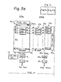
- a prior art dual-port type dynamic RAM device includes a dynamic RAM portion 100 and a serial data input and output (I/O) portion 200.
- the dynamic RAM portion 100 includes a dynamic RAM cell array 1, a sense amplifier group 2, first and second gate groups 3 and 4, a column decoder 5, a row decoder 6, an amplifier circuit 7, an I/O circuit 8, and a pair of data buses (DB and DB) 10 A and 10 B .
- the dynamic RAM portion 100 is of an open-bit line type, wherein each pair of bit lines BL i and BL i extends from both sides of the corresponding sense amplifier SA i .
- the dynamic RAM cell array 1 includes 64 Kbit of memory cells (MC's) connected between bits lines BL 0 to BL 255 and BL 0 to BL 255 and word lines WL 0 to WL 127 and WL 0 to WL 127 .
- the row decoder 6 receives a row address signal of eight bits RA 0 to RA 7 and energizes a word line defined by the received row address signal.
- the column decoder 5 also receives a column address signal of eight bits CA 0 to CA 7 and outputs a column decoded signal CDA defined by the received column address signal to the first and second gate groups 3 and 4.
- the sense amplifier group 2 consists of 256 sense amplifiers SA 0 to SA 255 , each operatively connected to a pair of corresponding bit lines BL . and BL . .
- the first gate group 3 consists of 256 gates GA 0 to GA 255 , each connected between the data bus 10 A and the corresponding bit line BL..
- the second gate group 4 also consists of 256 gates GH 0 to GB 255 , each connected between another data bus 10 B and the correspoding bit line BL i .
- bit lines BL 0 to BL 255 and BL 0 to BL 255 are precharged.
- a pair of word lines WL. and WL i and a pair of dummy word lines are selected by the row decoder 6 in response to the row address sgnal of RA 0 to RA 7 , connecting a plurality of memory cells MC between the selected word lines WL i and WL i and the bit lines BL 0 to BL 255 and BL 0 to BL 255 .
- the voltage difference based on the content stored in each . memory cell i.e., "1" or "0" appears on each bit line.
- the sense amplifiers SA 0 to SA 255 are rendered to an active state and amplify the voltage differences on the bit lines.
- One of each pair of bit lines becomes high level, e.g., approximately the power source voltage level V CC , and the other becomes low level, for example, the ground level V SS .
- the column decoder 5 is operated and outputs a column decoded signal CD. to gates of a pair of gates GA i and GB i in response to the received column address signal CA 0 to CA 7 , resulting in the connection of the corresponding bit lines BL. and BL i to the data buses 10A and 10 B through the corresponding gates GA i and GB., respectively.
- Stored data in the selected memory cell is detected at the amplifier circuit 7 and is output to a port (not shown) through the I/O circuit 8.
- a port (not shown) through the I/O circuit 8.
- data to be stored is supplied to the port and is stored in the corresponding memory cell through the I/O circuit 8 and the amplifier circuit 7.
- the serial I/O portion 200 is provided outside of the dynamic RAM portion 100.
- the serial I/O portion 200 includes transfer gate group 21A, a latch circuit group 22, a serial gate grpup 23, a shift register group 24, another column decoder 25, an amplifier circuit 26, and an I/O circuit 27.
- the transfer gate group 21A consists of 256 gates TGA O to TGA 255 connected to the bit lines BL 0 to BL255.
- the latch circuit group 22 consists of 256 flip-flops FF 0 to FF255 , each having a set input terminal connected to the corresponding transfer gate TGA i .
- the serial gate group 23 consists of 256 gates SG 0 to SG 255 , each having a terminal connected to an output terminal of the corresponding flip-flop FF i and another terminal connected to a serial data bus (SDB) 20.
- the shift register group 24 consists of 256 shift registers SR 0 to SR 255 connected in cascade to form a ring counter.
- the bit lines are precharged and the pair of word lines and the dummy word lines are selected, whereby a plurality of data in the memory cells selected by the word lines are sensed at the sense amplifiers, set forth above.
- a transfer clock signal TCLK A is supplied to the transfer gate group 21A, 256 gates TGA 0 to TGA 255 , which are formed by metal-oxide semiconductor field-effect transistors (MOS FET's), are turned ON during a time for the application of a transfer clock signal TCLK A , transferring 256 data on the bit lines BL 0 to BL 255 to the flip-flops FF 0 to FF255 , thus holding the data in the flin-floas.
- MOS FET's metal-oxide semiconductor field-effect transistors
- the column decoder 25 receives the column address signal of CA 0 to CA 7 , independently from the application of it to the column decoder 5 and outputs a column decoded signal CDB . defined by the received column address signal of CA 0 to CA 7 to the corresponding shift register SR j .
- the column decoded signal CDB. indicates a first location of data read from the flip-flops.
- the j-th shift register BR energizes a j-th serial gate SG j to turn the gate ON, outputting data stored in j-th flip-flop FF. to the serial data bus 20.
- the data on the serial data bus 20 is amplified at the amplifier circuit 26 and output as an output data SS OUT to another port through the I/O circuit 27.
- a clock signal is supplied to the shift register group 24
- data of "1" in the j-th shift register SR j is transferred to the (j+l)-th shift register SR j+1 , outputting the next data stored in the (j+1)-th flip-flop FF j+1 to another port.
- Similar operation may follow consecutively, serially outputting up to 256 data once stored in the flip-flops FF 0 to FF 255 to another port without further transferring data from the dynamic RAM cell array 1. Accordingly, a large amount of data can be. easily and rapidly output.
- a large data store may be also effected in a similar way set forth above.
- Provision of the above serial data I/O portion 200 enables high-speed data input and output in addition to a normal random access operation in the dynamic RAM portion 100. This, however, increases the complexity of the circuit and thus reduces the integration of the circuit in a chip. It also results in high power consumption in the chip. These disadvantages are serious ones in semiconductor memory devices, especially dynamic RAM devices.
- the dynamic RAM device shown in Fig. 1 is provided with two independent column decoders 5 and 25, one column decoder 5 activating the gate groups 3 and 4 and another column decoder 25 designating a start location for serial data input and output.
- Figure 2 is a circuit diagram of a part of the column decoder 5.
- i- and j-th column decoding circuits are shown.
- a plurality of pairs of column address signal lines A 0 and a 0 to A 7 and A 7 extend in parallel in the column decoder 5.
- eight transistors Q l to Q 8 are provided between lines L 1 and L 2 .
- Gates thereof are connected to one side of the plurality of pairs of column address signal lines so that an i-th column decoded signal CDA i is output when the plurality of pairs of column address signal A 0 and A O to A 7 and A 7 indicate the number "i".
- 256 column decoding circuits each of which is formed similar to the i- or j-th column decoding circuit shown in Fig. 2, are provided.
- Another column decoder 25 is also provided with 256 column decoding circuits, each of which is formed similar to that in the column decoder 5.
- Each dynamic RAM device includes a dynamic RAM portion 100A, 100B and a serial data I/O portion 200A, 200B.
- Each dynamic RAM device has the same circuit construction as that shown in Fig. 1.
- the dynamic RAM devices are operable independently from each other.
- four column decoders 5A, 5B, 25A, and 25B are provided.
- the column decoders 5A and 5B activate gates for data buses, while the column decoders 25A and 25B designate start locations of serial data input and output.
- Each column decoder is naturally formed similar to that shown in Fig. 2.
- the column decoder 5 may operate in a random data access mode.
- the column decoder 25 may operate in a serial data input and output operation mode and in a short period for designating the first data input and output location to the corresponding shift register. This enables the deletion of the column decoder 25 and common use of the column decoder 5 for the random data access as well as the serial data input and output.
- the common use of the column decoder 5 will cause no conflict between random access means and the serial access means as long as only a single set of column address receiving circuitry is provided in the semiconductor memory device since only one column address can be applied to the semiconductor memory device at a time regardless of the access mode. This concept can be applied to the dynamic RAM devices shown in Fig. 3.
- FIG. 4 a circuit diagram of an embodiment of a semiconductor memory device is shown.
- the semiconductor memory device in Fig. 4 is of an open-bit line type dynamic RAM device as shown in Fig. 1.
- the dynamic RAM device in Fig. 4 includes a dynamic RAM portion 100 and a serial data I/O portion 200'.
- the dynamic RAM portion 100 is identical to that shown in Fig. 1.
- the serial data I/O portion 200' does not include the column decoder 25 shown in Fig. 1.
- the shift register group 24 receives column decoded signals CD O to CD 255 from the column decoder 5 instead of the column decoder 25.
- the decoding circuit shown in Fig.2 is still used for the column decoder 5 in Fig. 4.
- the operation of the i-th column decoding circuit will be described.
- a reset pulse R is supplied to gates of MOS transistors Q 12 and Q 13 , resulting in the column decoded signal CD i being the low level of the ground level V SS and the potential of the line L 1 being pulled-up to the high level V CC .
- a column decoded signal CD i of high level is output upon receipt of the column decoder selection signal CDS of high level.
- the column decoding circuit is formed as a NOR gate circuit.
- the selected column decoded signal CD i is used for gating i-th gates GA i and GB i in the gate groups 3 and 4 in the random access operation mode or for setting one to the i-th shift register SR i in the serial data input and output operation mode.
- the i-th shift register SR i includes a depletion (D)-type transistor Q 50 , a pair of enhancement (E)-type transistors Q 51 and Q 52 forming a flip-flop, E-type transistors Q 53 to Q 55 , series-connected E-type transistors Q 56 and Q 57 , an E-type transistor Q 58 , an E-type transistor Q 59 , a pair of E-type transistors Q 60 and Q61 forming a flip-flop, a D-type transistor Q 62 , and a capacitor C 50 of a depletion layer of a transistor.
- D depletion
- E enhancement
- a source of the transistor Q 53 is supplied with a first clock pulse P 1 for driving shift registers.
- a gate of the transistor Q 56 is supplied with a transfer clock signal TLK' which is high level in the serial data input and output operation mode and enables setting of one bit to a shift register in response to the column decoded signal.
- a gate of the transistor Q 57 receives the i-th column decoded signal CD i .
- the (i+1)-th shift register SR j+1 has a similar circuit construction to that of the shift register SR i .
- a transistor Q 73 receives a second clock pulse P 2 for driving shift registers.
- the D-type transistor Q 50 ' Q 62 ' Q 70 and Q 82 can be replaced with resistors.
- Figures 6a and 6b are views of waveforms of the first and second clock pulses P 1 and P 2 for driving the shift registers.
- the clock pulses P 1 and P 2 differ in phase by 180°.
- the reset pulse R is supplied to gates of transistors Q 55 and Q 75 , resulting in voltage levels at nodes SP i and SL i in the register SR i and SP i+1 and SL i+1 in the register SR i+1 being at low level, the flip-flops formed by the pairs of transistors Q51 ' Q 52 ' Q60 ' Q 61 ' Q 71 ' Q 72 and Q 80 , Q 81 being reset, and thus pointer outputs PO i and P i+1 ' connected to gates of i- and (i+l)-th serial gates SG i and SG i+l in the serial data gate group 23, being low level.
- the content previously stored in the i-th flip-flop FF i in the flip-flop group 22 is transferred to the serial data bus 20, coutputting the data on the serial data bus 20 to another port through the amplifier circuit 26 and the I/O circuit 27.
- the i-th pointer output PO i is supplied to a gate of the transistor Q 78 parallel- connected to a series circuit of the transistors Q76 and Q 77 , in the adjoining shift egister SR i+1 , charging the nodes SP i+1 and SL i+1 up at high level and rendering the flip-flop of the transistors Q 80 and Q 81 in the SET state. Due to the application of the second clock P 2 to the transistor Q73 , the flip-flop of the transistors Q 71 and Q 72 is set, outputting the (i+l)-th pointer output PO i+1 of high level to the (i+1)-th gate SG i+1 .
- the (i+1)-th pointer command PO i+1 is supplied to a gate of the transistor Q 59 forming a reset gate of the flip-flop of the transistors Q60 and Q 61 .
- the flip-flop of the transistors Q 60 and Q 61 as well as the flip-flop of the transistors Q 51 and Q 52 in the preceding step of the shift register SR i are reset.
- the i-th pointer output PO i is restored to low level. This means that the logical "1" data stored in the shift register SR i is shifted to the following shift register SR i+1 .
- the (i+1)-th data stored in the (i+1)-th flip-flop FF i+1 is output to another port in the same way as described above.
- the first clock P 1 is supplied to the (i+2)-th shift register SR i+2 , the (i+2)-th pointer output PO i+2 of high level is output and the (i+1)-th pointer output PO i+1 becomes low level.
- the above operation is continued for a desired number times for serially outputting desired data.
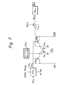
- the circuit of the o-th filp- flop FF and the connection between the flip-flop FF and the relevant circuits i.e., the serial data gates SGA 0 and SGB O , the transfer care TG O , the sense amplifier SA O , and the serial data buses SDB and SDB, are shown.
- the flip-flop FF consists of MOS transistors Q 41 and Q 42 and is connected to an active pull-up circuit 22a.
- the serial data bus (SDB) 20 is shown as a single data bus.
- complementary-type data buses SDB and SDB which may increase the reliability of sensing data, are shown. Accordingly, a pair of serial data gates SGA 0 and SGB 0 connecting the flip-flop FF o to the data buses SDB and SDB are provided.
- the complementary serial data buses SDB and SDB can naturally be applied to the circuit shown in Fig. 4.
- the dynamic RAM device can effect both the random data access operation and high-speed serial data input and output operation. Due to the deletion of the column decoder 25 and common use of the column decoder 5 for the random data access operation and the designation of the first location to the shift registers in the serial data input and output operation mode, there is achieved a dynamic RAM device with reduced circuit complexity, use of space, and power consumption.
- the circuits of the shift registers and the flip-flops FF are simple. This may increase the above effects.
- Figure 8 is a circuit diagram of another embodiment of a semiconductor memory device in accordance with the present invention.
- the semiconductor memory device is an open-bit line type dual port dynamic RAM device similar to that in Fig. 4.
- the dynamic RAM device in question includes four data buses (DBl to DB4) 10 1 to 10 4 , four amplifier circuits 7 1 to 7 4 , and a multiplexer 9 in a dynamic RAM portion 100b.
- the dynamic RAM device also includes four serial data buses (SDBl to SDB4) 20 1 to 20 4 , four amplifier circuits 26 1 to 26 4 , and a multiplexer 28 in a serial data I/O portion 200b.
- the addition of the data buses 10 1 to 10 4 and the serial data buses 20 1 to 20 4 greatly improves the access time of the dynamic RAM cell.
- the multiplexer 9 performs the multiplexing of data from and to the amplifier circuits 7 1 to 7 4 in a predetermined time interval during the random access mode.
- the multiplexer 28 performs the multiplexing of data from and to the amplifier circuits 26 1 to 26 4 in a predetermined time interval during the serial data input and output mode.
- first and second gate groups 3A and 4A Due to the addition of the data buses, the circuit connection of first and second gate groups 3A and 4A is somewhat changed from that in Fig. 4.
- the connection of the serial data gate group 23 to the serial data buses 20 1 to 20 4 is also changed.
- Four gates, such as G 0 and G 1 in the first gate group 3A and G 2 and G 3 in the second gate group 4A, may be triggered in a group by one column decoded signal, such as CD O .
- four serial gates, such as SG 0 to SG 3 in the serial data gate group 23, may be triggered in a group. Accordingly, a column decoder 5' does not require the column address signal of A 6 , A 6 and A 7 , A 7 , thus is simplified as shown in Fig. 9.
- a shift register group 24' has, accordingly, only 64 shift registers SR 0 to SR 63 '
- the predecoder circuit 50 includes an address drive clock circuit 51, tandem-connected gates 52 and 53 for shifting the level of a signal output from the circuit 51, a column decoder activating circuit 54 generating the column decoder activation signal CDA, and a 1/4 decoder 55.
- the 1/4 decoder 55 receives the column address signal A 6 and A 7 and the column decoder activation signal CDA and outputs column decoder selection signals CDS 0 to CDS 3 .
- MOS transistors Q 90 to Q 95 the connection of which is represented by a general form, correspond to, for example, transistors Q 1 to Q 6 shown in Fig. 9.
- a flip-flop circuit of MOS transistors Q 15 and Q 16 and a capacitor C 10 are provided.
- Another flip-flop circuit of MOS transistors Q 35 and Q 36 and a capacitor C 30 are also provided.
- Other transistors Q 14 ' Q 17 , Q 18 , and Q 19 correspond to the transistors Q 12 , Q 10 , Q 11 , and Q 13 shown in Fig. 9, respectively.
- a folded-bit line type dual ports dynamic RAM device is shown.
- the dynamic RAM device includes a dynamic RAM portion 100C and a serial data I/O portion 200C.
- a part of the circuit shown in Fig. 11 is shown in detail, the circuit of Fig. 12 corresponds to that of Fig. 7.
- the transfer gate group 21' in Fig. 11 consists of 256 pairs of transfer gates, each pair of gates, such as TGA 0 and TGB O , being provided between the sense amplifier SA 0 and the flip-flop FF o and connected to the pair of bit lines BL 0 and BL 0 .
- a column decoder 5 activates either a gate group 3 connected between a sense amplifier group 2 and a data bus 10 in the dynamic RAM portion 100C or a shift register group 24 in the serial data input and output portion 200C, in response to the random access mode or the serial data input and output mode.
- Other circuit constructions and operations are similar to those of Fig. 4.
- FIG. 13 another folded-bit type dual port dynamic RAM device is shown.
- the dynamic RAM device includes four data buses 10 1 to 10 4 and four serial data buses 20 1 to 20 4 , as shown in Fig. 8. Accordingly, the circuit construction and operation of Fig. 8 can be applied to the dynamic RAM device in Fig. 13 in the same way, except for the connection between the bit lines and the transfer gates, shown in Fig. 12.
- FIGs. 14a and 14b the operation timings of the common column decoder 5' in Fig. 13 will be described.
- shaded portions represent operation times of the column decoder 5'.
- Figure 14a represents operation times for the random access in a dynamic RAM portion 100d. Each operation time for random access is T I .
- Figure 14b represents operation times for the serial data input and output. Each operation time of the column decoder for the serial data input and output is T 2 .
- the subsequent operation time T 3 not the shaded portion, shows an operation for serial data input and output after once storing 256 data from the dynamic RAM cell portion 1' into 256 flip-flops FF 0 to FF255.
- the dynamic RAM cell portion I' includes 64 Kbit of memory cells. Assuming the random access for four data requires 250 nanoseconds (ns), the above time T 1 is 250 ns. Assuming also the time for selecting one pair of word lines WL i and WL i and transferring 256 data on the bit lines BL O , BL O to BL 255 ' BL 255 to the flip-flops FF 0 to FF 255 requires 250 ns, the time T 2 is also 250 ns.
- the time T 3 is 10.24 us.
- the column decoder 5' operates for the time T 1 for each request.
- the column decoder 5' operates for the time T 2 , equal to the time T 1 .
- the subsequent serial data transfer in the serial data input and output portion 200d is effected during a considerably long time T 3'
- the column decoder 5' is available for the random access mode operation. Even if use of the column decoder 5' overlapps at the time t 3 , the random access operation may be delayed by the time ⁇ 1 .
- the serial data input and output operation at the time t 5 may be delayed by the time T2 .
- these time delays ⁇ 1 and T2 are less than 250 ns in this example. Consequently, the actual decline in performance in the random access and/or the serial data input and output, even upon overlapping of requests, is negligible.
- FIG. 15 a circuit of two dynamic RAM devices on a chip in accordance with the present invention, which is improved over the circuit of the dynamic RAM devices shown in Fig. 3, is shown.
- Each dynamic RAM device includes a dynamic RAM portion 100e, 100f and a serial data input and output portion 200e, 200f.
- a single column decoder 5 is provided for the two dynamic RAM devices, resulting in a great reduction of space used by the circuit.
- Figure 16 is a part of a schematic layout of an example concerning the circuit shown in Fig. 11.
- the column decoder 5 is provided between the gate group 3 and the shift register group 24.
- the serial gate group 23 is provided adjacent to the flip-flop group 24. The many bit lines between the sense amplifier group 2 and the transfer gate group 21' and the lines between the transfer gate group 21' and the flip-flop group 22 should also be minimized in length.
Abstract
Description
- The present invention relates to a semiconductor memory device. More particularly, it relates to a semiconductor memory device having a high-speed serial data input and output circuit in addition to a random data input and output circuit.
- An image data processing system or the like requires a large-capacity memory. To meet the requirement for a large-capacity memory at low cost, a dynamic random-access memory (RAM) is extensively used. In addition, in order to display a large amount of image data stored in the RAM on a cathode ray tube (CRT) display unit and perform image data processing for a large amount of image data, such as gradients and filtering, high-speed data store and/or read-out are also highly required. A normal semiconductor memory device having a dynamic RAM and operable for random access for each data, per se, however, suffers from a disadvantage of low-speed data store and/or read-out for a large amount of image data.
- Recently, in order to overcome the above disadvantage, there have been proposed so-called dual-port memory devices, i.e., semiconductor memory devices including a high-speed data input and output circuit provided outside the dynamic RAM. A dual-port memory device is operable for not only normal random access through a conventional port, but also high-speed serial data input and output used by a high-speed data input and output circuit through another port.
- These prior art semiconductor memory devices, however, still suffer from disadvantages of complex circuit configurations and the use of a considerably large space on the semiconductor chip, which may lead to low integration, and high power consumption.
- It is accordingly desirable to provide a semiconductor memory device having a serial data inpur and output circuit with low-cost, large-capacity memory cells; reduced complexity of circuit configuration and use of space on a chip; and low power consumption.
- According to an embodiment of the present invention, there is provided- a semiconductor memory device including: at least one memory cell array including a plurality of memory cells arranged in a matrix form with a plurality of bit lines and a plurality of word lines, a circuit, operatively connected to the memory cell array, for selecting one of the word lines in response to an address signal, and a plurality of gates, operatively connected between the bit lines and at least one data bus, for transferring data to be stored or read between the bit lines and the data bus. The semiconductor memory device also includes a circuit for serially data input and output, including a plurality of transfer gates, operatively connected to the bit lines, and operable in a group in response to a transfer clock pulse, a plurality of latch circuits having terminals operatively connected to the transfer gates and holding data to be stored or read, a plurality of serial gates, having terminals operatively connected to other terminals of the latch circuits and having other terminals connected to at least one serial data bus, and a plurality of ring-connected shift registers triggering the serial gates, a single bit being shifted therethrough. The semiconductor memory device further includes a decoding circuit operatively connected to the gates and triggering at least one of the gates in response to another address signal in a random access operation mode and operatively connected to the shift registers and setting a single bit to a corresponding shift register in response to the column address signal in a serial data input and output operation mode. The serial data input and output circuit is operable independently from the memory cell array, except during a time for operatively connecting the bit lines and the latch circuits through the transfer gates, for serially inputting data to or outputting data from the latch circuits through the serial data bus by sequentially triggering the serial gates from a certain gate designated by the corresponding shift register in response to the decoding circuit.
- Preferably, the decoding circuit is operated only during the time for operatively connecting the bit lines and the latch circuits in the serial data input and output operation mode.
- Reference will now be made, by way of example, to the- accompanying drawings, in which:
- Fig. 1 is a circuit diagram of a prior art semiconductor memory device having a high-speed serial input and output circuit;
- Fig. 2 is a circuit diagram of a part of a column decoder shown in Fig. 1;
- Fig. 3 is a circuit diagram of another prior art semiconductor memory device including twc memory systems, each having a high-speed serial input and output circuit;
- Fig. 4 is a circuit diagram of an embodiment of a semiconductor memory device having a high-speed serial input and output circuit in accordance with the present invention;
- Fig. 5 is a circuit diagram of a part of a serial register array shown in Fig. 4;
- Figs. 6a and 6b are views of waveforms of clock pulses applied to the serial register array shown in Fig. 5;
- Fig. 7 is a circuit diagram of sense amplifiers, transfer gates, serial transfer gates, filp-flops, and shift registers shown in Fig. 4;
- Fig. 8 is a circuit diagram of another embodiment of a semiconductor memory device in accordance with the present invention;
- Fig. 9 is a circuit diagram of an example of a part of a column decoder shown in Fig. 8;
- Fig. 10 is a circuit diagram of another example of a part of a column decoder and a circuit relevant to the column decoder shown in Fig. 8;
- Fig. 11 is a circuit diagram of still another embodiment of a semiconductor memory device in accordance with the present invention;
- Fig. 12 is a circuit diagram of sense amplifiers, transfer gates, serial transfer gates, flip-flops, and shift registers shown in Fig. ll;
- Fig. 13 is a circuit diagram of yet another embodiment of a semiconductor memory device in accordance with the present invention;
- Figs. 14a and 14b are timing charts illustrating the operation of a column decoder shown in Fig. 13;
- Fig. 15 is a circuit diagram of another embodiment of a semiconductor memory device in accordance with the present invention; and
- Fig. 16 is a schematic layout of a part of the semiconductor memory device shown in Fig. 11.
- Before describing preferred embodiments of the present invention, an explanation will be given of the prior art for reference.
- Referring to Fig. 1, a prior art dual-port type dynamic RAM device includes a
dynamic RAM portion 100 and a serial data input and output (I/O)portion 200. Thedynamic RAM portion 100 includes a dynamicRAM cell array 1, asense amplifier group 2, first andsecond gate groups column decoder 5, arow decoder 6, anamplifier circuit 7, an I/O circuit 8, and a pair of data buses (DB andDB) 10A and 10B. Thedynamic RAM portion 100 is of an open-bit line type, wherein each pair of bit lines BLi andBL i RAM cell array 1 includes 64 Kbit of memory cells (MC's) connected between bits linesBL 0 BL 255 WL 0 WL 127 . Therow decoder 6 receives a row address signal of eight bits RA0 to RA7 and energizes a word line defined by the received row address signal. Thecolumn decoder 5 also receives a column address signal of eight bits CA0 to CA7 and outputs a column decoded signal CDA defined by the received column address signal to the first andsecond gate groups sense amplifier group 2 consists of 256 sense amplifiers SA0 to SA255 , each operatively connected to a pair of corresponding bit lines BL. and BL.. Thefirst gate group 3 consists of 256 gates GA0 to GA255 , each connected between thedata bus 10A and the corresponding bit line BL.. Thesecond gate group 4 also consists of 256 gates GH0 to GB255 , each connected between anotherdata bus 10B and the correspoding bit lineBL i . - In a random access mode for data read, the bit lines BL0 to BL255 and
BL 0 BL 255 WL i row decoder 6 in response to the row address sgnal of RA0 to RA7 , connecting a plurality of memory cells MC between the selected word lines WLi andWL i BL 0 BL 255 . As a result, the voltage difference based on the content stored in each . memory cell, i.e., "1" or "0", appears on each bit line. The sense amplifiers SA0 to SA255 are rendered to an active state and amplify the voltage differences on the bit lines. One of each pair of bit lines becomes high level, e.g., approximately the power source voltage level VCC , and the other becomes low level, for example, the ground level VSS. After that, thecolumn decoder 5 is operated and outputs a column decoded signal CD. to gates of a pair of gates GAi and GBi in response to the received column address signal CA0 to CA7 , resulting in the connection of the corresponding bit lines BL. andBL i data buses amplifier circuit 7 and is output to a port (not shown) through the I/O circuit 8. In a random access mode for data store, data to be stored is supplied to the port and is stored in the corresponding memory cell through the I/O circuit 8 and theamplifier circuit 7. - The serial I/
O portion 200 is provided outside of thedynamic RAM portion 100. The serial I/O portion 200 includestransfer gate group 21A, alatch circuit group 22, aserial gate grpup 23, ashift register group 24, anothercolumn decoder 25, anamplifier circuit 26, and an I/O circuit 27. Thetransfer gate group 21A consists of 256 gates TGAO to TGA255 connected to the bit lines BL0 to BL255. Thelatch circuit group 22 consists of 256 flip-flops FF0 to FF255 , each having a set input terminal connected to the corresponding transfer gate TGAi. Theserial gate group 23 consists of 256 gates SG0 to SG255 , each having a terminal connected to an output terminal of the corresponding flip-flop FFi and another terminal connected to a serial data bus (SDB) 20. Theshift register group 24 consists of 256 shift registers SR0 to SR255 connected in cascade to form a ring counter. - In a serial access mode for data read, the bit lines are precharged and the pair of word lines and the dummy word lines are selected, whereby a plurality of data in the memory cells selected by the word lines are sensed at the sense amplifiers, set forth above. As a transfer clock signal TCLKA is supplied to the
transfer gate group column decoder 25 receives the column address signal of CA0 to CA7, independently from the application of it to thecolumn decoder 5 and outputs a column decoded signal CDB. defined by the received column address signal of CA0 to CA7 to the corresponding shift register SRj. The column decoded signal CDB. indicates a first location of data read from the flip-flops. Upon receipt of the column decoded signal CDB. , the j-th shift register BR energizes a j-th serial gate SGj to turn the gate ON, outputting data stored in j-th flip-flop FF. to theserial data bus 20. The data on theserial data bus 20 is amplified at theamplifier circuit 26 and output as an output data SSOUT to another port through the I/O circuit 27. As a clock signal is supplied to theshift register group 24, data of "1" in the j-th shift register SRj is transferred to the (j+l)-th shift register SRj+1, outputting the next data stored in the (j+1)-th flip-flop FFj+1to another port. Similar operation may follow consecutively, serially outputting up to 256 data once stored in the flip-flops FF0 to FF255 to another port without further transferring data from the dynamicRAM cell array 1. Accordingly, a large amount of data can be. easily and rapidly output. A large data store may be also effected in a similar way set forth above. - Provision of the above serial data I/
O portion 200 enables high-speed data input and output in addition to a normal random access operation in thedynamic RAM portion 100. This, however, increases the complexity of the circuit and thus reduces the integration of the circuit in a chip. It also results in high power consumption in the chip. These disadvantages are serious ones in semiconductor memory devices, especially dynamic RAM devices. - In particular, the dynamic RAM device shown in Fig. 1 is provided with two
independent column decoders column decoder 5 activating thegate groups column decoder 25 designating a start location for serial data input and output. Figure 2 is a circuit diagram of a part of thecolumn decoder 5. In Fig. 2, i- and j-th column decoding circuits are shown. A plurality of pairs of column address signal lines A0 and a0 to A7 and A7 extend in parallel in thecolumn decoder 5. With respect to the i-th column decoding circuit, eight transistors Ql to Q8 are provided between lines L1 and L2. Gates thereof are connected to one side of the plurality of pairs of column address signal lines so that an i-th column decoded signal CDAi is output when the plurality of pairs of column address signal A0 and AO to A7 and A7 indicate the number "i". In thecolumn decoder - Another
column decoder 25 is also provided with 256 column decoding circuits, each of which is formed similar to that in thecolumn decoder 5. - Referring to Fig. 3, two dynamic RAM devices are formed in a chip. Each dynamic RAM device includes a
dynamic RAM portion O portion 200A, 200B. Each dynamic RAM device has the same circuit construction as that shown in Fig. 1. The dynamic RAM devices are operable independently from each other. In Fig. 3, fourcolumn decoders column decoders column decoders 25A and 25B designate start locations of serial data input and output. Each column decoder is naturally formed similar to that shown in Fig. 2. - Referring back to Fig. 1, note that the two
column decoders column decoder 5 may operate in a random data access mode. Thecolumn decoder 25 may operate in a serial data input and output operation mode and in a short period for designating the first data input and output location to the corresponding shift register. This enables the deletion of thecolumn decoder 25 and common use of thecolumn decoder 5 for the random data access as well as the serial data input and output. In addition, the common use of thecolumn decoder 5 will cause no conflict between random access means and the serial access means as long as only a single set of column address receiving circuitry is provided in the semiconductor memory device since only one column address can be applied to the semiconductor memory device at a time regardless of the access mode. This concept can be applied to the dynamic RAM devices shown in Fig. 3. - Preferred embodiments of the present invention will now be described in detail.
- Referring to Fig. 4, a circuit diagram of an embodiment of a semiconductor memory device is shown. The semiconductor memory device in Fig. 4 is of an open-bit line type dynamic RAM device as shown in Fig. 1. The dynamic RAM device in Fig. 4 includes a
dynamic RAM portion 100 and a serial data I/O portion 200'. Thedynamic RAM portion 100 is identical to that shown in Fig. 1. On the other hand, the serial data I/O portion 200' does not include thecolumn decoder 25 shown in Fig. 1. Theshift register group 24 receives column decoded signals CDO to CD255 from thecolumn decoder 5 instead of thecolumn decoder 25. - The decoding circuit shown in Fig.2 is still used for the
column decoder 5 in Fig. 4. The operation of the i-th column decoding circuit will be described. In an initial condition, a reset pulse R is supplied to gates of MOS transistors Q12 and Q13 , resulting in the column decoded signal CDi being the low level of the ground level VSS and the potential of the line L1 being pulled-up to the high level VCC. When the column address signal A0 , A0 to A7 , A7 does not coincide with the number "i", at least one of the MOS transistors Q1 to Q8 is turned ON, thus a short-circuit is made between the lines L1 and L2 , whereupon a column decoded signal CDi of low level is output, unless a column decoder selection signal CDS of high level is supplied to a source of a MOS transistor Q10. On the other hand, when the column address signal indicates the number "i", all transistors Q1 to Q8 are turned OFF, thus the line L1 is kept at high level. This high voltage is supplied to a gate of the transistor Q10 through a MOS transistor Q11. Accordingly, upon receipt of the column decoder selection signal CDS of high level, a column decoded signal CDi of high level is output. In this case, other column decoded signals CD0 to CDi-1 and CDi+1 to CD255 are naturally low level. As can be seen from the description, the column decoding circuit is formed as a NOR gate circuit. Referring back to Fig. 4, the selected column decoded signal CDi is used for gating i-th gates GAi and GBi in thegate groups - Referring to Fig. 5, the circuit of the i- and (i+l)-th shift registers SRi and SRi+1 is shown. The i-th shift register SRi includes a depletion (D)-type transistor Q50 , a pair of enhancement (E)-type transistors Q51 and Q52 forming a flip-flop, E-type transistors Q53 to Q55 , series-connected E-type transistors Q56 and Q57 , an E-type transistor Q58 , an E-type transistor Q59 , a pair of E-type transistors Q60 and Q61 forming a flip-flop, a D-type transistor Q62 , and a capacitor C50 of a depletion layer of a transistor. A source of the transistor Q53 is supplied with a first clock pulse P1 for driving shift registers. A gate of the transistor Q56 is supplied with a transfer clock signal TLK' which is high level in the serial data input and output operation mode and enables setting of one bit to a shift register in response to the column decoded signal. A gate of the transistor Q57 receives the i-th column decoded signal CDi. The (i+1)-th shift register SRj+1 has a similar circuit construction to that of the shift register SRi. However, a transistor Q73 receives a second clock pulse P2 for driving shift registers. The D-type transistor Q50 ' Q62 ' Q70 and Q82 can be replaced with resistors.
- The operation of the shift registers shown in Fig. 5 will be described with reference to Figs. 6a and 6b. Figures 6a and 6b are views of waveforms of the first and second clock pulses P1 and P2 for driving the shift registers. The clock pulses P1 and P2 differ in phase by 180°.
- In an initial condition, the reset pulse R is supplied to gates of transistors Q55 and Q75 , resulting in voltage levels at nodes SPi and SLi in the register SRi and SPi+1 and SLi+1 in the register SRi+1 being at low level, the flip-flops formed by the pairs of transistors Q51 ' Q52 ' Q60 ' Q61 ' Q71 ' Q72 and Q80, Q81 being reset, and thus pointer outputs POi and Pi+1 ' connected to gates of i- and (i+l)-th serial gates SGi and SGi+l in the serial
data gate group 23, being low level. When a column decoded signal CDi of high level is supplied to the gate of the transistor Q57 and the clock pulse TLK' is supplied to the gate of the transistor Q56 , the node SPi is charged up, rendering the flip-flop of the transistors Q60 and Q61 in the SET state and charging the node SLi up to high level. Due to the application of the first clock pulse P1 to the source of the transistor Q53 , the flip-flop of the transistors Q51 and Q52 is set and thus the i-th pointer output POi of high level is output. Due to the application of the pointer output POi of high level to the i-th gate SGi , the content previously stored in the i-th flip-flop FFi in the flip-flop group 22 is transferred to theserial data bus 20, coutputting the data on theserial data bus 20 to another port through theamplifier circuit 26 and the I/O circuit 27. Simultaneously, the i-th pointer output POi is supplied to a gate of the transistor Q78 parallel- connected to a series circuit of the transistors Q76 and Q77 , in the adjoining shift egister SRi+1 , charging the nodes SPi+1 and SLi+1 up at high level and rendering the flip-flop of the transistors Q80 and Q81 in the SET state. Due to the application of the second clock P2 to the transistor Q73 , the flip-flop of the transistors Q71 and Q72 is set, outputting the (i+l)-th pointer output POi+1 of high level to the (i+1)-th gate SGi+1. At this time, the (i+1)-th pointer command POi+1 is supplied to a gate of the transistor Q59 forming a reset gate of the flip-flop of the transistors Q60 and Q61. The flip-flop of the transistors Q60 and Q61 as well as the flip-flop of the transistors Q51 and Q52 in the preceding step of the shift register SRi are reset. As a result, the i-th pointer output POi is restored to low level. This means that the logical "1" data stored in the shift register SRi is shifted to the following shift register SRi+1. In this case, the (i+1)-th data stored in the (i+1)-th flip-flop FFi+1 is output to another port in the same way as described above. When the first clock P1 is supplied to the (i+2)-th shift register SRi+2 , the (i+2)-th pointer output POi+2 of high level is output and the (i+1)-th pointer output POi+1 becomes low level. The above operation is continued for a desired number times for serially outputting desired data. - Referring to Fig. 7, the circuit of the o-th filp- flop FF and the connection between the flip-flop FF and the relevant circuits, i.e., the serial data gates SGA0 and SGBO , the transfer care TGO , the sense amplifier SAO , and the serial data buses SDB and SDB, are shown. The flip-flop FF consists of MOS transistors Q41 and Q42 and is connected to an active pull-up
circuit 22a. In Fig. 4, the serial data bus (SDB) 20 is shown as a single data bus. In Fig. 7, however, complementary-type data buses SDB and SDB, which may increase the reliability of sensing data, are shown. Accordingly, a pair of serial data gates SGA0 and SGB0 connecting the flip-flop FFo to the data buses SDB and SDB are provided. The complementary serial data buses SDB and SDB can naturally be applied to the circuit shown in Fig. 4. - As can be seen from the description with reference to Figs. 4 to 7, in spite of the deletion of the
column decoder 25 shown in Fig. 1, the dynamic RAM device can effect both the random data access operation and high-speed serial data input and output operation. Due to the deletion of thecolumn decoder 25 and common use of thecolumn decoder 5 for the random data access operation and the designation of the first location to the shift registers in the serial data input and output operation mode, there is achieved a dynamic RAM device with reduced circuit complexity, use of space, and power consumption. - The circuits of the shift registers and the flip-flops FF are simple. This may increase the above effects.
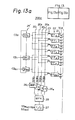
- Figure 8 is a circuit diagram of another embodiment of a semiconductor memory device in accordance with the present invention.
- The semiconductor memory device is an open-bit line type dual port dynamic RAM device similar to that in Fig. 4. The dynamic RAM device in question, however, includes four data buses (DBl to DB4) 101 to 104 , four
amplifier circuits 71 to 74 , and amultiplexer 9 in adynamic RAM portion 100b. The dynamic RAM device also includes four serial data buses (SDBl to SDB4) 201 to 204 , fouramplifier circuits 261 to 264 , and amultiplexer 28 in a serial data I/O portion 200b. The addition of thedata buses 101 to 104 and theserial data buses 201 to 204 greatly improves the access time of the dynamic RAM cell. Themultiplexer 9 performs the multiplexing of data from and to theamplifier circuits 71 to 74 in a predetermined time interval during the random access mode. Themultiplexer 28 performs the multiplexing of data from and to theamplifier circuits 261 to 264 in a predetermined time interval during the serial data input and output mode. - Due to the addition of the data buses, the circuit connection of first and
second gate groups data gate group 23 to theserial data buses 201 to 204 is also changed. Four gates, such as G0 and G1 in thefirst gate group 3A and G2 and G3 in thesecond gate group 4A, may be triggered in a group by one column decoded signal, such as CDO. Similarly, four serial gates, such as SG0 to SG3 in the serialdata gate group 23, may be triggered in a group. Accordingly, a column decoder 5' does not require the column address signal of A6 , A6 and A7 , A7 , thus is simplified as shown in Fig. 9. A shift register group 24' has, accordingly, only 64 shift registers SR0 to SR63' - The principle of the operation of the dynamic RAM device shown in Fig. 8 is the same to that of the dynamic RAM device shown in Fig. 4, thus a description thereof is omitted.
- Referring to Fig. 10, a circuit diagram of another example showing a part of a
column decoder 5" corresponding to that in Fig. 9 and apredecoder circuit 50 are shown. Thepredecoder circuit 50 includes an addressdrive clock circuit 51, tandem-connectedgates circuit 51, a columndecoder activating circuit 54 generating the column decoder activation signal CDA, and a 1/4decoder 55. The 1/4decoder 55 receives the column address signal A6 and A7 and the column decoder activation signal CDA and outputs column decoder selection signals CDS0 to CDS3. In thecolumn decoder 5", MOS transistors Q90 to Q95 the connection of which is represented by a general form, correspond to, for example, transistors Q1 to Q6 shown in Fig. 9. In order to improve the operational reliability, a flip-flop circuit of MOS transistors Q15 and Q16 and a capacitor C10 are provided. Another flip-flop circuit of MOS transistors Q35 and Q36 and a capacitor C30 are also provided. Other transistors Q14 ' Q17 , Q18 , and Q19 correspond to the transistors Q12 , Q10 , Q11 , and Q13 shown in Fig. 9, respectively. - Referring to Fig. 11, a folded-bit line type dual ports dynamic RAM device is shown.
- Each pair of bit lines, such as BL0 and BL0 , are folded at the sense amplifier SAO. This type of bit line arrangement may increase the resistance against noise. The dynamic RAM device includes a dynamic RAM portion 100C and a serial data I/O portion 200C. Referring to Fig. 12, a part of the circuit shown in Fig. 11 is shown in detail, the circuit of Fig. 12 corresponds to that of Fig. 7. The transfer gate group 21' in Fig. 11 consists of 256 pairs of transfer gates, each pair of gates, such as TGA0 and TGBO , being provided between the sense amplifier SA0 and the flip-flop FFo and connected to the pair of bit lines BL0 and
BL0 . Acolumn decoder 5 activates either agate group 3 connected between asense amplifier group 2 and adata bus 10 in the dynamic RAM portion 100C or ashift register group 24 in the serial data input and output portion 200C, in response to the random access mode or the serial data input and output mode. Other circuit constructions and operations are similar to those of Fig. 4. - Referring to Fig. 13, another folded-bit type dual port dynamic RAM device is shown. The dynamic RAM device includes four
data buses 101 to 104 and fourserial data buses 201 to 204 , as shown in Fig. 8. Accordingly, the circuit construction and operation of Fig. 8 can be applied to the dynamic RAM device in Fig. 13 in the same way, except for the connection between the bit lines and the transfer gates, shown in Fig. 12. - Referring to Figs. 14a and 14b, the operation timings of the common column decoder 5' in Fig. 13 will be described. In Figs. 14a and 14b, shaded portions represent operation times of the column decoder 5'. Figure 14a represents operation times for the random access in a
dynamic RAM portion 100d. Each operation time for random access is TI. Figure 14b represents operation times for the serial data input and output. Each operation time of the column decoder for the serial data input and output is T2. The subsequent operation time T3 , not the shaded portion, shows an operation for serial data input and output after once storing 256 data from the dynamic RAM cell portion 1' into 256 flip-flops FF0 to FF255. - The dynamic RAM cell portion I' includes 64 Kbit of memory cells. Assuming the random access for four data requires 250 nanoseconds (ns), the above time T1 is 250 ns. Assuming also the time for selecting one pair of word lines WLi and WLi and transferring 256 data on the bit lines BLO , BLO to BL255 ' BL 255 to the flip-flops FF0 to FF255 requires 250 ns, the time T2 is also 250 ns. Furthermore, assuming the time for serially outputting 256 data stored in the flip-flops to another port through
amplifier circuits 261 to 264 , amultiplexer 28, and an I/O circuit 27 requires 40 ns x 256, i.e., 10.24 microseconds (ps), the time T3 is 10.24 us. When random accesses are requested at the times t1 and t2 , the column decoder 5' operates for the time T1 for each request. When a serial data input and output is requested at the time t3 , the column decoder 5' operates for the time T2 , equal to the time T1. The subsequent serial data transfer in the serial data input andoutput portion 200d is effected during a considerably long time T3' Note that during the time T3 , the column decoder 5' is available for the random access mode operation. Even if use of the column decoder 5' overlapps at the time t3 , the random access operation may be delayed by the time τ1. On the contrary, the serial data input and output operation at the time t5 may be delayed by the time T2. However, these time delays τ1 and T2 are less than 250 ns in this example. Consequently, the actual decline in performance in the random access and/or the serial data input and output, even upon overlapping of requests, is negligible. - If the
multiplexers - Referring to Fig. 15, a circuit of two dynamic RAM devices on a chip in accordance with the present invention, which is improved over the circuit of the dynamic RAM devices shown in Fig. 3, is shown. Each dynamic RAM device includes a
dynamic RAM portion output portion single column decoder 5 is provided for the two dynamic RAM devices, resulting in a great reduction of space used by the circuit. - In the above description, the circuit configurations and the operations of the embodiments were discussed. In addition, consideration must be given to a circuit arrangement minimizing the lines between the column decoder and the gate group(s) 3 (and 4) connected to the
data bus 10, lines between the column decoder and theshift register group 24, lines between thesense amplifier group 2 and thetransfer gate group 21, and other lines. Figure 16 is a part of a schematic layout of an example concerning the circuit shown in Fig. 11. Thecolumn decoder 5 is provided between thegate group 3 and theshift register group 24. Theserial gate group 23 is provided adjacent to the flip-flop group 24. The many bit lines between thesense amplifier group 2 and the transfer gate group 21' and the lines between the transfer gate group 21' and the flip-flop group 22 should also be minimized in length. - Many widely different embodiments of the present invention may be constructed without departing from the spirit and scope of the present invention. It should be understood that the present invention is not limited to the specific embodiments described in this specification, except as defined in the appended claims.
Claims (19)
the number of said memory cell arrays being equal to the number of said serial input and output circuits.
Applications Claiming Priority (2)
| Application Number | Priority Date | Filing Date | Title |
|---|---|---|---|
| JP313/85 | 1985-01-05 | ||
| JP60000313A JPS61160898A (en) | 1985-01-05 | 1985-01-05 | Semiconductor memory device |
Publications (3)
| Publication Number | Publication Date |
|---|---|
| EP0188134A2 true EP0188134A2 (en) | 1986-07-23 |
| EP0188134A3 EP0188134A3 (en) | 1988-08-10 |
| EP0188134B1 EP0188134B1 (en) | 1991-09-25 |
Family
ID=11470421
Family Applications (1)
| Application Number | Title | Priority Date | Filing Date |
|---|---|---|---|
| EP85309562A Expired - Lifetime EP0188134B1 (en) | 1985-01-05 | 1985-12-31 | Semiconductor memory device having serial data input and output circuit |
Country Status (7)
| Country | Link |
|---|---|
| US (1) | US4769789A (en) |
| EP (1) | EP0188134B1 (en) |
| JP (1) | JPS61160898A (en) |
| KR (1) | KR900008935B1 (en) |
| CA (1) | CA1246741A (en) |
| DE (1) | DE3584241D1 (en) |
| IE (1) | IE57268B1 (en) |
Cited By (5)
| Publication number | Priority date | Publication date | Assignee | Title |
|---|---|---|---|---|
| DE3727688A1 (en) * | 1986-08-19 | 1988-02-25 | Toshiba Kawasaki Kk | SEMICONDUCTOR STORAGE SYSTEM |
| FR2623320A1 (en) * | 1987-11-18 | 1989-05-19 | Sony Corp | MEMORY OF DYNAMIC TYPE |
| EP0325105A1 (en) * | 1988-01-19 | 1989-07-26 | Kabushiki Kaisha Toshiba | Multiport memory |
| EP0363031A1 (en) * | 1988-09-20 | 1990-04-11 | Fujitsu Limited | Serial input/output semiconductor memory |
| EP0422965A2 (en) * | 1989-10-13 | 1991-04-17 | Texas Instruments Incorporated | Circuit for continuous processing of video signals in a synchronous vector processor |
Families Citing this family (16)
| Publication number | Priority date | Publication date | Assignee | Title |
|---|---|---|---|---|
| JPS6142795A (en) * | 1984-08-03 | 1986-03-01 | Toshiba Corp | Row decoder system of semiconductor memory device |
| JPS6240698A (en) * | 1985-08-16 | 1987-02-21 | Fujitsu Ltd | Semiconductor memory device |
| JPS62146490A (en) * | 1985-12-20 | 1987-06-30 | Sanyo Electric Co Ltd | Semiconductor memory |
| US4807198A (en) * | 1987-12-28 | 1989-02-21 | Motorola, Inc. | Memory input buffer with hysteresis and dc margin |
| JP2591010B2 (en) * | 1988-01-29 | 1997-03-19 | 日本電気株式会社 | Serial access memory device |
| NL8802125A (en) * | 1988-08-29 | 1990-03-16 | Philips Nv | INTEGRATED MEMORY CIRCUIT WITH PARALLEL AND SERIAL INPUT AND OUTPUT. |
| JPH0283899A (en) * | 1988-09-20 | 1990-03-23 | Fujitsu Ltd | Semiconductor memory |
| JP2993671B2 (en) * | 1989-01-07 | 1999-12-20 | 三菱電機株式会社 | Semiconductor storage device |
| US4984214A (en) * | 1989-12-05 | 1991-01-08 | International Business Machines Corporation | Multiplexed serial register architecture for VRAM |
| JPH05182454A (en) * | 1991-06-25 | 1993-07-23 | Mitsubishi Electric Corp | Dual port memory device |
| US5355335A (en) * | 1991-06-25 | 1994-10-11 | Fujitsu Limited | Semiconductor memory device having a plurality of writing and reading ports for decreasing hardware amount |
| DE69226150T2 (en) * | 1991-11-05 | 1999-02-18 | Hsu Fu Chieh | Redundancy architecture for circuit module |
| AU4798793A (en) * | 1992-08-10 | 1994-03-03 | Monolithic System Technology, Inc. | Fault-tolerant, high-speed bus system and bus interface for wafer-scale integration |
| US5535172A (en) * | 1995-02-28 | 1996-07-09 | Alliance Semiconductor Corporation | Dual-port random access memory having reduced architecture |
| US6167486A (en) | 1996-11-18 | 2000-12-26 | Nec Electronics, Inc. | Parallel access virtual channel memory system with cacheable channels |
| US6708254B2 (en) | 1999-11-10 | 2004-03-16 | Nec Electronics America, Inc. | Parallel access virtual channel memory system |
Citations (3)
| Publication number | Priority date | Publication date | Assignee | Title |
|---|---|---|---|---|
| EP0056240A2 (en) * | 1981-01-08 | 1982-07-21 | Nec Corporation | Memory device |
| EP0097778A2 (en) * | 1982-06-30 | 1984-01-11 | International Business Machines Corporation | Digital storage |
| WO1984001230A1 (en) * | 1982-09-23 | 1984-03-29 | Motorola Inc | Serial data mode circuit for a memory |
Family Cites Families (4)
| Publication number | Priority date | Publication date | Assignee | Title |
|---|---|---|---|---|
| NL7713706A (en) * | 1977-12-12 | 1979-06-14 | Philips Nv | INFORMATION BUFFER MEMORY OF THE "FIRST-IN, FIRST-OUT" TYPE WITH A VARIABLE INPUT AND A VARIABLE OUTPUT. |
| US4498155A (en) * | 1979-11-23 | 1985-02-05 | Texas Instruments Incorporated | Semiconductor integrated circuit memory device with both serial and random access arrays |
| JPS5727477A (en) * | 1980-07-23 | 1982-02-13 | Nec Corp | Memory circuit |
| US4586167A (en) * | 1983-01-24 | 1986-04-29 | Mitsubishi Denki Kabushiki Kaisha | Semiconductor memory device |
-
1985
- 1985-01-05 JP JP60000313A patent/JPS61160898A/en active Pending
- 1985-12-30 US US06/814,388 patent/US4769789A/en not_active Expired - Lifetime
- 1985-12-30 CA CA000498754A patent/CA1246741A/en not_active Expired
- 1985-12-31 KR KR1019850010094A patent/KR900008935B1/en not_active IP Right Cessation
- 1985-12-31 EP EP85309562A patent/EP0188134B1/en not_active Expired - Lifetime
- 1985-12-31 DE DE8585309562T patent/DE3584241D1/en not_active Expired - Fee Related
-
1986
- 1986-01-03 IE IE17/86A patent/IE57268B1/en not_active IP Right Cessation
Patent Citations (3)
| Publication number | Priority date | Publication date | Assignee | Title |
|---|---|---|---|---|
| EP0056240A2 (en) * | 1981-01-08 | 1982-07-21 | Nec Corporation | Memory device |
| EP0097778A2 (en) * | 1982-06-30 | 1984-01-11 | International Business Machines Corporation | Digital storage |
| WO1984001230A1 (en) * | 1982-09-23 | 1984-03-29 | Motorola Inc | Serial data mode circuit for a memory |
Cited By (8)
| Publication number | Priority date | Publication date | Assignee | Title |
|---|---|---|---|---|
| DE3727688A1 (en) * | 1986-08-19 | 1988-02-25 | Toshiba Kawasaki Kk | SEMICONDUCTOR STORAGE SYSTEM |
| FR2623320A1 (en) * | 1987-11-18 | 1989-05-19 | Sony Corp | MEMORY OF DYNAMIC TYPE |
| US5280448A (en) * | 1987-11-18 | 1994-01-18 | Sony Corporation | Dynamic memory with group bit lines and associated bit line group selector |
| EP0325105A1 (en) * | 1988-01-19 | 1989-07-26 | Kabushiki Kaisha Toshiba | Multiport memory |
| US5007028A (en) * | 1988-01-19 | 1991-04-09 | Kabushiki Kaisha Toshiba | Multiport memory with improved timing of word line selection |
| EP0363031A1 (en) * | 1988-09-20 | 1990-04-11 | Fujitsu Limited | Serial input/output semiconductor memory |
| EP0422965A2 (en) * | 1989-10-13 | 1991-04-17 | Texas Instruments Incorporated | Circuit for continuous processing of video signals in a synchronous vector processor |
| EP0422965A3 (en) * | 1989-10-13 | 1993-09-22 | Texas Instruments Incorporated | Circuit for continuous processing of video signals in a synchronous vector processor and method of operating same |
Also Published As
| Publication number | Publication date |
|---|---|
| CA1246741A (en) | 1988-12-13 |
| EP0188134B1 (en) | 1991-09-25 |
| JPS61160898A (en) | 1986-07-21 |
| EP0188134A3 (en) | 1988-08-10 |
| US4769789A (en) | 1988-09-06 |
| KR860006135A (en) | 1986-08-18 |
| DE3584241D1 (en) | 1991-10-31 |
| KR900008935B1 (en) | 1990-12-13 |
| IE57268B1 (en) | 1992-07-01 |
Similar Documents
| Publication | Publication Date | Title |
|---|---|---|
| US4769789A (en) | Semiconductor memory device having serial data input and output circuit | |
| KR940000148B1 (en) | Dual port semiconductor memory device | |
| US4733376A (en) | Semiconductor memory device having serial data input circuit and serial data output circuit | |
| JP2740063B2 (en) | Semiconductor storage device | |
| US6377503B1 (en) | Synchronous dynamic random access memory | |
| US4875196A (en) | Method of operating data buffer apparatus | |
| US4394753A (en) | Integrated memory module having selectable operating functions | |
| US5398213A (en) | Access time speed-up circuit for a semiconductor memory device | |
| JP2002063791A (en) | Semiconductor memory and memory system | |
| JPH05159567A (en) | Dual-port memory | |
| EP0187289A2 (en) | Hierarchical memory system | |
| EP0388175B1 (en) | Semiconductor memory device | |
| EP0366588B1 (en) | Memory organization with arrays having an alternate data port facility | |
| JP2000315390A (en) | Integrated circuit having memory cell storing data bit and method for writing write-in data bit in memory cell in integrated circuit | |
| US5523979A (en) | Semiconductor memory device for block access applications | |
| EP0062547A2 (en) | Memory circuit | |
| US4485461A (en) | Memory circuit | |
| JPS61500573A (en) | semiconductor memory | |
| JP2575061B2 (en) | Semiconductor storage device | |
| JPS62287498A (en) | Semiconductor memory unit | |
| US6285617B1 (en) | Semiconductor memory device preventing malfunction during refresh operation even when noise is superimposed on control signal | |
| JPH0289288A (en) | Semiconductor memory | |
| JPH0330184A (en) | Semiconductor storage device | |
| JPS63152091A (en) | Dynamic ram | |
| JPH0316083A (en) | Semiconductor memory device |
Legal Events
| Date | Code | Title | Description |
|---|---|---|---|
| PUAI | Public reference made under article 153(3) epc to a published international application that has entered the european phase |
Free format text: ORIGINAL CODE: 0009012 |
|
| AK | Designated contracting states |
Kind code of ref document: A2 Designated state(s): DE FR GB |
|
| PUAL | Search report despatched |
Free format text: ORIGINAL CODE: 0009013 |
|
| AK | Designated contracting states |
Kind code of ref document: A3 Designated state(s): DE FR GB |
|
| 17P | Request for examination filed |
Effective date: 19880922 |
|
| 17Q | First examination report despatched |
Effective date: 19900315 |
|
| GRAA | (expected) grant |
Free format text: ORIGINAL CODE: 0009210 |
|
| AK | Designated contracting states |
Kind code of ref document: B1 Designated state(s): DE FR GB |
|
| REF | Corresponds to: |
Ref document number: 3584241 Country of ref document: DE Date of ref document: 19911031 |
|
| ET | Fr: translation filed | ||
| PLBE | No opposition filed within time limit |
Free format text: ORIGINAL CODE: 0009261 |
|
| STAA | Information on the status of an ep patent application or granted ep patent |
Free format text: STATUS: NO OPPOSITION FILED WITHIN TIME LIMIT |
|
| 26N | No opposition filed | ||
| PGFP | Annual fee paid to national office [announced via postgrant information from national office to epo] |
Ref country code: GB Payment date: 19931001 Year of fee payment: 9 |
|
| PGFP | Annual fee paid to national office [announced via postgrant information from national office to epo] |
Ref country code: DE Payment date: 19940224 Year of fee payment: 9 |
|
| PG25 | Lapsed in a contracting state [announced via postgrant information from national office to epo] |
Ref country code: GB Effective date: 19941231 |
|
| GBPC | Gb: european patent ceased through non-payment of renewal fee |
Effective date: 19941231 |
|
| PG25 | Lapsed in a contracting state [announced via postgrant information from national office to epo] |
Ref country code: DE Effective date: 19950901 |
|
| PGFP | Annual fee paid to national office [announced via postgrant information from national office to epo] |
Ref country code: FR Payment date: 19971209 Year of fee payment: 13 |
|
| PG25 | Lapsed in a contracting state [announced via postgrant information from national office to epo] |
Ref country code: FR Free format text: LAPSE BECAUSE OF NON-PAYMENT OF DUE FEES Effective date: 19990831 |
|
| REG | Reference to a national code |
Ref country code: FR Ref legal event code: ST |