EP0189039A2 - Card with a microprocessor and/or at least an electronic memory - Google Patents
Card with a microprocessor and/or at least an electronic memory Download PDFInfo
- Publication number
- EP0189039A2 EP0189039A2 EP86100075A EP86100075A EP0189039A2 EP 0189039 A2 EP0189039 A2 EP 0189039A2 EP 86100075 A EP86100075 A EP 86100075A EP 86100075 A EP86100075 A EP 86100075A EP 0189039 A2 EP0189039 A2 EP 0189039A2
- Authority
- EP
- European Patent Office
- Prior art keywords
- core
- film
- conductors
- layers
- card
- Prior art date
- Legal status (The legal status is an assumption and is not a legal conclusion. Google has not performed a legal analysis and makes no representation as to the accuracy of the status listed.)
- Withdrawn
Links
Images

Classifications
-
- G—PHYSICS
- G06—COMPUTING; CALCULATING OR COUNTING
- G06K—GRAPHICAL DATA READING; PRESENTATION OF DATA; RECORD CARRIERS; HANDLING RECORD CARRIERS
- G06K19/00—Record carriers for use with machines and with at least a part designed to carry digital markings
- G06K19/06—Record carriers for use with machines and with at least a part designed to carry digital markings characterised by the kind of the digital marking, e.g. shape, nature, code
- G06K19/067—Record carriers with conductive marks, printed circuits or semiconductor circuit elements, e.g. credit or identity cards also with resonating or responding marks without active components
- G06K19/07—Record carriers with conductive marks, printed circuits or semiconductor circuit elements, e.g. credit or identity cards also with resonating or responding marks without active components with integrated circuit chips
- G06K19/072—Record carriers with conductive marks, printed circuits or semiconductor circuit elements, e.g. credit or identity cards also with resonating or responding marks without active components with integrated circuit chips the record carrier comprising a plurality of integrated circuit chips
-
- G—PHYSICS
- G06—COMPUTING; CALCULATING OR COUNTING
- G06K—GRAPHICAL DATA READING; PRESENTATION OF DATA; RECORD CARRIERS; HANDLING RECORD CARRIERS
- G06K19/00—Record carriers for use with machines and with at least a part designed to carry digital markings
- G06K19/06—Record carriers for use with machines and with at least a part designed to carry digital markings characterised by the kind of the digital marking, e.g. shape, nature, code
- G06K19/067—Record carriers with conductive marks, printed circuits or semiconductor circuit elements, e.g. credit or identity cards also with resonating or responding marks without active components
- G06K19/07—Record carriers with conductive marks, printed circuits or semiconductor circuit elements, e.g. credit or identity cards also with resonating or responding marks without active components with integrated circuit chips
- G06K19/077—Constructional details, e.g. mounting of circuits in the carrier
- G06K19/07743—External electrical contacts
Definitions
- the present invention relates to cards such as "credit cards" which are provided with a microprocessor and / or at least one electronic memory capable of storing data of all kinds such as individual codes, credits in one or more currencies, data personal medical, etc., and if necessary carry out certain operations on this data according to a determined program contained in the microprocessor in response to signals which are delivered to it by an electronic device external to the card with which the latter can be connected to using visible contacts connected to the microprocessor and the memories contained in the card.
- cards such as "credit cards” which are provided with a microprocessor and / or at least one electronic memory capable of storing data of all kinds such as individual codes, credits in one or more currencies, data personal medical, etc., and if necessary carry out certain operations on this data according to a determined program contained in the microprocessor in response to signals which are delivered to it by an electronic device external to the card with which the latter can be connected to using visible contacts connected to the microprocessor and the memories contained in the card.
- the object of the present invention is to produce such an electronic card which is inviolable.
- the present invention relates to an electronic card provided with a microprocessor and / or at least one electronic memory which overcomes the aforementioned drawbacks.
- This card comprising contacts accessible from the outside thereof, characterized in that it consists of several layers of compatible plastics, compositions, and characteristics different, forming a monolithic assembly, by the fact that these layers are at least three in number, a core comprising at least one local hard core having at least one recess and two protective layers of thinner thickness than the core covering the two upper and lower faces of this core; by the fact that a film comprising a printed circuit whose outputs are connected to an integrated circuit comprising a microprocessor and / or at least one electronic memory is disposed between the core and one of the protective layers at the location of the hard local core, the integrated circuit being housed at least partially in the recess of this hard core; and by the fact that the outputs of the printed circuit are connected by conductors to the contacts of the card, these conductors also being located between the core and said protective layer.
- the electronic card illustrated in the drawing comprises several layers of compatible plastics, of different compositions and characteristics, made monolithic by hot rolling.
- the central layer or core is composite formed of a plastic sheet i comprising two through openings, one containing a hard core 2 provided with a recess 3 and the other containing a plastic plate 4 incorporating an identification or marking as a watermark.
- the hard core 2 comprises a non-through recess 3 opening into a recess 5 which one of the faces of this core 2 has.
- This portion of film 6 is placed in the recess 5 of the hard core 2, the integrated circuit or chip 7 being placed in the recess 3 of this hard core 2.
- the output terminals of the printed circuit carried by the film 6 are connected to the contacts 8, accessible from outside the card, by conductors 9.
- the portion of film 6 carrying the printed circuit has openings 10 placed in such a way that all the connections connecting the output terminals of the printed circuit to the terminals of the integrated circuit (s) pass through these openings 10.
- the illustrated card also includes printed plastic sheets 11,12 located on either side of the core 1,2 as well as transparent protective layers 13,14 located on the free faces of the printed sheets 11,12.
- the five layers, ie the core 1,2, the printed sheets 11,12 and the protective layers 13,14 are made monolithic by hot rolling, the different plastics forming these layers being compatible.
- the printed sheet 13 is made integral, by the hot rolling of the hard core 2 around at least part of all the connections of the printed circuit carried by this film 6. Thus, it is impossible to separate the core 1,2 from the layer which is superimposed on it, in this example layer 11, without destroying the printed circuit which makes the card inviolable.
- the core 1,2 can be made of white opaque plastic with a thickness of 0.40 mm
- the printed sheets, bearing indications of use of the card, a trademark or any other indication useful to the user may be of a thickness of 0.20 mm tinted in the mass for example, and that the layers of protection are transparent with a thickness of 0.06 mm so that the inscriptions carried by the printed sheets are visible.
- the film 6 carrying the printed circuit is generally in Kapton (trademark registered by Du Pont de Nemours) and even if this plastic material is incompatible with the plastics forming the core 1,2 and the printed layer 11, the card is inviolable thanks to the openings 10 made in this film 6 allowing an intimate connection between the layers 1,2 and 11 around each connection of the printed circuit and therefore the destruction of these during an attempt to separate these two layers.
- Kapton trademark registered by Du Pont de Nemours
- the number of integrated circuits 7 is arbitrary and depends on the functions of the card, these integrated circuits can be electronic memories or microprocessors or a combination of these elements.
- either or even the two printed layers can be omitted, the protective layers 13, 14 then being directly linked to the core 1,2.
- these protective layers are not necessarily transparent, and may themselves be mass-colored or include inscriptions in their mass.
- the recess 3 of the hard core 2 in which the integrated circuit is housed could be through and once the integrated circuit housed in this hole, the rest of it is filled with an epoxy or silicone resin to completely coat said integrated circuit.
- the conductors connecting the contacts of the card to the terminals of the integrated circuit can be carried by the film 6, it may then be that part of this film exceeds the hard core 2.
- the card is composed of a core 15 provided on its lower and upper faces with two protective layers 16, 17; this core and these layers being made of hot-rollable plastic material.
- the electronic part of the card is entirely carried by a film 18 in Kapton (registered trademark) having openings 19, here two in the example illustrated, intended to receive integrated circuits.
- Kapton registered trademark
- the upper surface at least of this film 18 comprises tinned copper conductors 20 which are glued to the film 18. These conductors have one end connected to a contact 21 whose free surface is generally gold-plated and another end extending beyond from the edge of the film inside one of the openings 19. This end 22 is intended to be welded to a contact 23 of an integrated circuit 24.
- the contacts 21 are accessible from the outside of the card by a slot 25 in the protective layer 17.
- the film 18 provided with the conductors 20 and the integrated circuits 24, is placed in the desired position between the core 15 and the protective layer 17.
- the three layers 15,16,17 are hot rolled which has the effect of heat sealing its layers to each other and also filling all the voids located around the conductors 20 and / or printed circuits by plastic deformation of the core in which the printed circuits are embedded 24.
- the card thus obtained is extremely robust, the film, the conductors and the integrated circuits being completely embedded in the mass of plastic material.
- the core 15 is heat-sealed to the protective layer 17 between each conductor 20 so that the card is tamper-proof; any attempt to separate the layers 17 and 15 leads to the destruction of the connections connecting the contacts 21 to the integrated circuits 24.
Abstract
Cette carte comporte des contacts (8) et se compose de plusieurs couches de matières plastiques (1, 2; 11, 12, 13, 14) compatibles. L'âme (1, 2) comporte au moins un noyau local (2) dur présentant un évidement (3). Deux couches de protection (13, 14) de plus faible épaisseur que l'àme recouvrent les deux faces supérieure et inférieure. Un film (6) comprend un circuit imprimé dont les sorties sont reliées à un circuit intégré (7) comportant un microprocesseur et/ou au moins une mémoire électronique est disposé entre i'âme (1, 2) et l'une des couches (13, 14) de protection à l'endroit du noyau local (2) dur. Le circuit intégré (7) est logé au moins partiellement dans l'évidement (3) de ce noyau (2) dur. Les sorties du circuit imprimé sont reliées par des conducteurs (9) aux contacts (8) de la carte, ces conducteurs étant également situés entre l'âme (1, 2) et ladite couche de protection (13).
Description
La présente invention se rapporte aux cartes type "cartes de crédit" qui sont munies d'un microprocesseur et/ou d'au moins une mémoire électronique pouvant stocker des données de tous genres telles que codes individuels, crédits en une ou plusieurs monnaies, données médicales personnelles, etc., et le cas échéant effectuer certaines opérations sur ces données selon un programme déterminé contenu dans le microprocesseur en réponse à des signaux qui lui sont délivrés par un appareillage électronique extérieur à la carte avec lequel celle-ci peut être branchée à l'aide de contacts apparents reliés au microprocesseur et aux mémoires contenus dans la carte.The present invention relates to cards such as "credit cards" which are provided with a microprocessor and / or at least one electronic memory capable of storing data of all kinds such as individual codes, credits in one or more currencies, data personal medical, etc., and if necessary carry out certain operations on this data according to a determined program contained in the microprocessor in response to signals which are delivered to it by an electronic device external to the card with which the latter can be connected to using visible contacts connected to the microprocessor and the memories contained in the card.
11 existe de telles cartes qui toutefois présentent l'inconvénient que le microprocesseur ou les mémoires peuvent être accessibles de l'extérieur de la carte et séparés de celle-ci ce qui peut permettre le décodage des informations contenues dans ceux-ci.There are such cards which, however, have the disadvantage that the microprocessor or the memories can be accessible from outside the card and separated from it, which can allow the decoding of the information contained therein.
Il est également connu du brevet US 3.702.464 une carte dans laquelle les conducteurs du circuit imprimé reliant le circuit intégré aux contacts sont apposés sur l'une des surfaces d'une des couches de matériel plastique. De telles cartes n'ont pas pu être réalisées car lors du laminage des couches de matière plastique les conducteurs fondent en coulant et se rejoignent formant des courts-circuits.It is also known from US Pat. No. 3,702,464 a card in which the conductors of the printed circuit connecting the integrated circuit to the contacts are affixed to one of the surfaces of one of the layers of plastic material. Such cards could not be produced because during the laminating of the plastic layers the conductors melt while flowing and join forming short-circuits.
La présente invention a pour but de réaliser une telle carte électronique qui soit inviolable.The object of the present invention is to produce such an electronic card which is inviolable.
La présente invention a pour objet une carte électronique munie d'un microprocesseur et/ou d'au moins une mémoire électronique obviant aux inconvénients précités. Cette carte comportant des contacts accessibles de l'extérieur de celle-ci, caractérisée par le fait qu'elle se compose de plusieurs couches de matières plastiquescompatibles, de compositions, et de caractéristiques différentes, formant un ensemble monolithique, par le fait que ces couches sont au moins au nombre de trois, une âme comportant au moins un noyau local dur présentant au moins un évidement et deux couches de protection de plus faible épaisseur que l'âme recouvrant les deux faces supérieure et inférieure de cette âme; par le fait qu'un film comprenant un circuit imprimé dont les sorties sont reliées à un circuit intégré comportant un microprocesseur et/ou au moins une mémoire électronique est disposé entre l'âme et l'une des couches de protection à l'endroit du noyau local dur, le circuit intégré étant logé au moins partiellement dans l'évidement de ce noyau dur; et par le fait que les sorties du circuit imprimé sont reliées par des conducteurs aux contacts de la carte, ces conducteurs étant également situés entre l'âme et ladite couche de protection.The present invention relates to an electronic card provided with a microprocessor and / or at least one electronic memory which overcomes the aforementioned drawbacks. This card comprising contacts accessible from the outside thereof, characterized in that it consists of several layers of compatible plastics, compositions, and characteristics different, forming a monolithic assembly, by the fact that these layers are at least three in number, a core comprising at least one local hard core having at least one recess and two protective layers of thinner thickness than the core covering the two upper and lower faces of this core; by the fact that a film comprising a printed circuit whose outputs are connected to an integrated circuit comprising a microprocessor and / or at least one electronic memory is disposed between the core and one of the protective layers at the location of the hard local core, the integrated circuit being housed at least partially in the recess of this hard core; and by the fact that the outputs of the printed circuit are connected by conductors to the contacts of the card, these conductors also being located between the core and said protective layer.
Le dessin annexé illustre schématiquement et à titre d' exemple une forme d'exécution de la carte électronique selon l'invention.The accompanying drawing illustrates schematically and by way of example an embodiment of the electronic card according to the invention.
- La figure 1 est une vue de dessus de la carte, une partie étant arrachée.Figure 1 is a top view of the card, a portion being cut away.
- La figure 2 est une coupe à plus grande échelle suivant la ligne II-II de la figure 1.FIG. 2 is a section on a larger scale along the line II-II of FIG. 1.
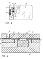
- La figure 3 illustre de dessus une variante de cette carte.Figure 3 illustrates from above a variant of this card.
- La figure 4 est une coupe partielle de la carte illustrée à la figure 3.FIG. 4 is a partial section of the card illustrated in FIG. 3.
La carte électronique illustrée au dessin comporte plusieurs couches de matières plastiques compatibles, de compositions et de caractéristiques différentes, rendues monolithiques par laminage à chaud.The electronic card illustrated in the drawing comprises several layers of compatible plastics, of different compositions and characteristics, made monolithic by hot rolling.
La couche centrale ou âme est composite formée d'une feuille i de matière plastique 1 comprenant deux ouvertures traversantes, l'une renfermant un noyau dur 2 muni d'un évidement 3 et l'autre renfermant une plaquette de matière plastique 4 incorporant une identification ou marquage sous forme de filigrane.The central layer or core is composite formed of a plastic sheet i comprising two through openings, one containing a
Dans la forme d'exécution illustrée le noyau dur 2 comporte un évidement 3 non traversant débouchant dans une creusure 5 que comporte l'une des faces de ce noyau 2.In the embodiment illustrated the
Une portion de film 6 découpée, comportant au moins un trou, porte un circuit imprimé dont les sorties sont reliées d'une part aux bornes d'un circuit intégré 7 situé dans le trou. Il s'agit d'une "tape automatic 'bonded chip" actuellement couramment utilisée en électronique.A cut portion of
Cette portion de film 6 est placée dans la creusure 5 du noyau dur 2, le circuit intégré ou chip 7 étant placé dans l'évidement 3 de ce noyau dur 2.This portion of
Les bornes de sortie du circuit imprimé porté par le film 6 sont reliées aux contacts 8, accessibles depuis l'extérieur de la carte, par des conducteurs 9.The output terminals of the printed circuit carried by the
La portion de film 6 portant le circuit imprimé comporte des ouvertures 10 placées de telle manière que toutes les connexions reliant les bornes de sorties du circuit imprimé aux bornes du ou des circuits intégrés traversent ces ouvertures 10.The portion of
La carte illustrée comporte encore des feuilles plastiques imprimées 11,12 situées de part et d'autre de l'âme 1,2 ainsi que des couches de protection transparentes 13,14 situées sur les faces libres des feuilles imprimées 11,12.The illustrated card also includes printed
Les cinq couches, soit l'âme 1,2, les feuilles imprimées 11,12 et les couches de protection 13,14 sont rendues monolithiques par laminage à chaud, les différents plastiques formant ces couches étant compatibles.The five layers, ie the
Du fait des ouvertures 10 pratiquées dans la portion de film 6, la feuille imprimée 13 est rendue solidaire, par le laminage à chaud du noyau dur 2 autour d'une partie au moins de toutes les connexions du circuit imprimé porté par ce film 6. Ainsi, il est impossible de séparer l'âme 1,2 de la couche qui lui est-superposée, dans cet exemple la couche 11, sans détruire le circuit imprimé ce qui rend la carte inviolable.Because of the
A titre d'exemple, on peut mentionner que l'âme 1,2 peut être en plastique opaque blanc d'une épaisseur de 0,40 mm, que les feuilles imprimées, portant des indications d'usage de la carte, une marque de fabrique ou tout autre indication utile à l'utilisateur, peuvent être d'une épaisseur de 0,20 mm teintées dans la masse par exemple, et que les couches de protection sont transparentes d'une épaisseur de 0,06 mm pour que les inscriptions portées par les feuilles imprimées soient visibles.By way of example, it may be mentioned that the
Le film 6 portant le circuit imprimé est généralement en Kapton (marque déposée par Du Pont de Nemours) et même si cette matière plastique est incompatible avec les matières plastiques formant l'âme 1,2 et la couche imprimée 11, la carte est inviolable grâce aux ouvertures 10 pratiquées dans ce film 6 permettant une liaison intime entre les couches 1,2 et 11 autour de chaque connexion du circuit imprimé et donc la destruction de celles-ci lors d'une tentative de séparation de ces deux couches.The
Du fait du noyau dur 2 de l'âme 1,2 au niveau du film 6 portant le circuit imprimé et le circuit intégré, et du fait que ce circuit intégré est logé dans un évidement de ce noyau dur 2 on obtient d'une part que l'épaisseur de la carte soit constante malgré l'épaisseur du circuit intégré 7 qui est plus grande que celle du film 6 et d'autre part une bonne protection de la partie électronique, circuit intégré et circuit imprimé, de la carte contre les chocs, pressions, déformations, etc. que peut subir cette carte.Due to the
De nombreuses variantes de la carte peuvent être prévues, le nombre de circuits intégrés 7 est arbitraire et dépend des fonctions de la carte, ces circuits intégrés peuvent être des mémoires électroniques ou des microprocesseurs ou une combinaison de ces éléments.Many variants of the card can be provided, the number of integrated circuits 7 is arbitrary and depends on the functions of the card, these integrated circuits can be electronic memories or microprocessors or a combination of these elements.
Dans une variante l'une ou l'autre, voire les deux couches imprimées peuvent être supprimées, les couches de protection 13, 14 étant alors directement liées à l'âme 1,2. Dans ces cas ces couches de protection ne sont pas nécessairement transparentes, et peuvent elles-mêmes être teintées dans la masse ou comporter des inscriptions dans leur masse.In one variant, either or even the two printed layers can be omitted, the
Il est évident qu'une exécution de la carte sans le noyau 4 comportant le filigrane peut être prévue.It is obvious that an execution of the card without the core 4 carrying the watermark can be provided.
En variante, l'évidement 3 du noyau dur 2 dans lequel est logé le circuit intégré pourrait être traversant et une fois le circuit intégré logé dans ce trou, le reste de celui-ci est rempli d'une résine époxy ou silicone pour enrober complètement ledit circuit intégré.Alternatively, the recess 3 of the
Dans une autre variante, les conducteurs reliant les contacts de la carte aux bornes du circuit intégré peuvent être portés par le film 6, il se peut alors qu'une partie de ce film dépasse le noyau dur 2.In another variant, the conductors connecting the contacts of the card to the terminals of the integrated circuit can be carried by the
C'est précisément une telle variante qui est illustrée aux " figures 3 et 4, elle présente notamment l'avantage de faciliter grandement la soudure des conducteurs collés sur le film aux bornes du ou des circuits intégrés.It is precisely such a variant which is illustrated in "Figures 3 and 4, it has in particular the advantage of greatly facilitating the soldering of the conductors bonded to the film at the terminals of the integrated circuit or circuits.
Dans cette variante illustrée aux figures 3 et 4 la carte est composée d'une âme 15 munie sur ses faces inférieur et supé- rieureae deux couches de protection 16,17; cette âme et ces couches étant en matériau plastique laminable à chaud.In this variant illustrated in FIGS. 3 and 4, the card is composed of a
La partie électronique de la carte est entièrement portée par un film 18 en Kapton (marque déposée) présentant des ouvertures 19, ici deux dans l'exemple illustré, destinée à recevoir des circuits intégrés.The electronic part of the card is entirely carried by a
La surface supérieur au moins de ce film 18 comporte des conducteurs en cuivre étamé 20 qui sont collés au film 18. Ces conducteurs ont une extrémité reliée à un contact 21 dont la surface libre est généralement dorée et une autre extrémité s'étendant au-delà du bord du film à l'intérieur d'une des ouvertures 19. Cette extrémité 22 est destinée à être soudée sur un contact 23 d'un circuit intégré 24. Les contacts 21 sont accessibles à partir de l'extérieur de la carte par une fente 25 pratiquée dans la couche de protection 17.The upper surface at least of this
Lorsque les conducteurs 20 sont collés sur le film 18, on peut facilement souder chaque extrémité 21 des conducteurs 20 sur le contact correspondant du ou des circuits intégrés 24. En effet les conducteurs 20 étant en cuivre on ne risque pas que ceux-ci fondent ou coulent. D'autre part l'absence de support de ces extrémités facilite cette soudure et empêche la création de courts-circuits.When the
Une fois la partie électronique ainsi terminée le film 18 muni des conducteurs 20 et des circuits intégrés 24, est placé dans la position voulue entre l'âme 15 et la couche de protection 17.Once the electronic part is thus finished, the
Enfin les trois couches 15,16,17 sont laminées à chaud ce qui a pour effet de thermosouder ses couches les unes aux autres et également de remplir tous les vides situés autour des conducteurs 20 et/ou des circuits imprimés par déformation plastique de l'âme dans laquelle viennent s'incruster les circuits imprimés 24.Finally the three
La carte ainsi obtenue est extrêmement robuste, le film, les conducteurs et les circuits intégrés étant complètement noyés dans la masse de matière plastique. De plus, l'âme 15 est thermo- soudée à la couche de protection 17 entre chaque conducteur 20 de sorte que la carte est inviolable; toute tentative de séparer les couches 17 etl5 entraîne la destruction des connexions reliant les contacts 21 aux circuits intégrés 24.The card thus obtained is extremely robust, the film, the conductors and the integrated circuits being completely embedded in the mass of plastic material. In addition, the
Claims (7)
Applications Claiming Priority (2)
| Application Number | Priority Date | Filing Date | Title |
|---|---|---|---|
| CH252/85A CH661808A5 (en) | 1985-01-21 | 1985-01-21 | CARD PROVIDED WITH A MICROPROCESSOR AND / OR AT LEAST ONE ELECTRONIC MEMORY. |
| CH252/85 | 1985-01-21 |
Publications (2)
| Publication Number | Publication Date |
|---|---|
| EP0189039A2 true EP0189039A2 (en) | 1986-07-30 |
| EP0189039A3 EP0189039A3 (en) | 1987-01-21 |
Family
ID=4182768
Family Applications (1)
| Application Number | Title | Priority Date | Filing Date |
|---|---|---|---|
| EP86100075A Withdrawn EP0189039A3 (en) | 1985-01-21 | 1986-01-04 | Card with a microprocessor and/or at least an electronic memory |
Country Status (4)
| Country | Link |
|---|---|
| US (1) | US4733061A (en) |
| EP (1) | EP0189039A3 (en) |
| CH (1) | CH661808A5 (en) |
| DE (1) | DE189039T1 (en) |
Cited By (9)
| Publication number | Priority date | Publication date | Assignee | Title |
|---|---|---|---|---|
| EP0263746A2 (en) * | 1986-10-02 | 1988-04-13 | Francelco, Societe Anonyme | System for reading identification cards with electrical contacts |
| EP0268830A2 (en) * | 1986-11-20 | 1988-06-01 | GAO Gesellschaft für Automation und Organisation mbH | Data carrier with integrated circuit and process for making the same |
| FR2624999A1 (en) * | 1987-12-22 | 1989-06-23 | Sgs Thomson Microelectronics | Method of manufacturing smart cards |
| FR2629666A1 (en) * | 1988-03-31 | 1989-10-06 | Toshiba Kk | INTEGRATED CIRCUIT CARD COMPRISING CIRCUIT MODULES FOR MOUNTING ELECTRONIC COMPONENTS |
| WO1990008365A1 (en) * | 1989-01-19 | 1990-07-26 | W. & T. Avery Limited | Portable electronic token |
| EP0706152A3 (en) * | 1994-11-03 | 1996-06-05 | Fela Holding Ag | Chip card and method for fabricating it |
| USRE35578E (en) * | 1988-12-12 | 1997-08-12 | Sgs-Thomson Microelectronics, Inc. | Method to install an electronic component and its electrical connections on a support, and product obtained thereby |
| WO1997042658A1 (en) * | 1996-05-06 | 1997-11-13 | Siemens Aktiengesellschaft | Chip card module with conductive plastic coating and process for manufacturing the same |
| FR2749687A1 (en) * | 1996-06-07 | 1997-12-12 | Solaic Sa | MEMORY CARD AND METHOD FOR MANUFACTURING SUCH A CARD |
Families Citing this family (13)
| Publication number | Priority date | Publication date | Assignee | Title |
|---|---|---|---|---|
| FR2597229B1 (en) * | 1986-04-11 | 1991-01-11 | Flonic Sa | ELECTRONIC MEMORY CARD PROCESSING DEVICE FOR PROVIDING BENEFITS |
| US5179517A (en) * | 1988-09-22 | 1993-01-12 | Bally Manufacturing Corporation | Game machine data transfer system utilizing portable data units |
| US5227338A (en) * | 1990-04-30 | 1993-07-13 | International Business Machines Corporation | Three-dimensional memory card structure with internal direct chip attachment |
| US5954583A (en) * | 1992-11-05 | 1999-09-21 | Com21 Limited | Secure access control system |
| US5451763A (en) * | 1994-07-05 | 1995-09-19 | Alto Corporation | Personal medical IC card and read/write unit |
| DE19611237A1 (en) * | 1996-03-21 | 1997-09-25 | Siemens Ag | Multichip card e.g. telephone card |
| FR2756955B1 (en) * | 1996-12-11 | 1999-01-08 | Schlumberger Ind Sa | METHOD FOR PRODUCING AN ELECTRONIC CIRCUIT FOR A CONTACTLESS MEMORY CARD |
| JP3173438B2 (en) * | 1997-06-04 | 2001-06-04 | ソニー株式会社 | Memory card and mounting device |
| DE19841551B4 (en) * | 1998-09-11 | 2006-01-05 | Donnelly Hohe Gmbh & Co. Kg | Electric rearview mirror |
| JP4470242B2 (en) * | 1999-04-23 | 2010-06-02 | ソニー株式会社 | Semiconductor memory card |
| US7810718B2 (en) * | 2005-05-12 | 2010-10-12 | Cubic Corporation | Variable thickness data card body |
| US10984304B2 (en) | 2017-02-02 | 2021-04-20 | Jonny B. Vu | Methods for placing an EMV chip onto a metal card |
| USD956760S1 (en) * | 2018-07-30 | 2022-07-05 | Lion Credit Card Inc. | Multi EMV chip card |
Citations (8)
| Publication number | Priority date | Publication date | Assignee | Title |
|---|---|---|---|---|
| US3702464A (en) * | 1971-05-04 | 1972-11-07 | Ibm | Information card |
| EP0029785A1 (en) * | 1979-11-27 | 1981-06-03 | Societe Flonic | Electrical connection system |
| GB2081950A (en) * | 1980-07-09 | 1982-02-24 | Philips Nv | A portable identifying element |
| GB2081644A (en) * | 1980-08-07 | 1982-02-24 | Gao Ges Automation Org | Identification card with an ic module and method of producing it |
| GB2095175A (en) * | 1981-03-24 | 1982-09-29 | Gao Ges Automation Org | An identification card having an ic-module |
| GB2096541A (en) * | 1981-04-14 | 1982-10-20 | Gao Ges Automation Org | An identification card having an ic module |
| EP0094716A1 (en) * | 1982-05-14 | 1983-11-23 | Rtc-Compelec | Process for connecting a semiconductor to elements of a support, particularly of a portable card |
| JPS58210646A (en) * | 1982-06-02 | 1983-12-07 | Kyodo Printing Co Ltd | Ic chip mold product |
Family Cites Families (1)
| Publication number | Priority date | Publication date | Assignee | Title |
|---|---|---|---|---|
| US4501960A (en) * | 1981-06-22 | 1985-02-26 | Motorola, Inc. | Micropackage for identification card |
-
1985
- 1985-01-21 CH CH252/85A patent/CH661808A5/en not_active IP Right Cessation
-
1986
- 1986-01-04 EP EP86100075A patent/EP0189039A3/en not_active Withdrawn
- 1986-01-04 DE DE198686100075T patent/DE189039T1/en active Pending
- 1986-01-06 US US06/816,614 patent/US4733061A/en not_active Expired - Lifetime
Patent Citations (8)
| Publication number | Priority date | Publication date | Assignee | Title |
|---|---|---|---|---|
| US3702464A (en) * | 1971-05-04 | 1972-11-07 | Ibm | Information card |
| EP0029785A1 (en) * | 1979-11-27 | 1981-06-03 | Societe Flonic | Electrical connection system |
| GB2081950A (en) * | 1980-07-09 | 1982-02-24 | Philips Nv | A portable identifying element |
| GB2081644A (en) * | 1980-08-07 | 1982-02-24 | Gao Ges Automation Org | Identification card with an ic module and method of producing it |
| GB2095175A (en) * | 1981-03-24 | 1982-09-29 | Gao Ges Automation Org | An identification card having an ic-module |
| GB2096541A (en) * | 1981-04-14 | 1982-10-20 | Gao Ges Automation Org | An identification card having an ic module |
| EP0094716A1 (en) * | 1982-05-14 | 1983-11-23 | Rtc-Compelec | Process for connecting a semiconductor to elements of a support, particularly of a portable card |
| JPS58210646A (en) * | 1982-06-02 | 1983-12-07 | Kyodo Printing Co Ltd | Ic chip mold product |
Non-Patent Citations (2)
| Title |
|---|
| ELECTRONIQUE INDUSTRIELLE, no. 15, 1er mai 1981, pages 87,88 PARIS (FR) "Carte de paiement-électronique: la version de LEP" * |
| PATENTS ABSTRACTS OF JAPAN, volume 8, no. 59 (E-232)(1496) 17 mars 1984 & JP-A-58 210 646 (KIYOUDOU INSATSU K.K.) 07-12-1983. * |
Cited By (13)
| Publication number | Priority date | Publication date | Assignee | Title |
|---|---|---|---|---|
| EP0263746B1 (en) * | 1986-10-02 | 1992-04-08 | Francelco, Societe Anonyme | System for reading identification cards with electrical contacts |
| EP0263746A2 (en) * | 1986-10-02 | 1988-04-13 | Francelco, Societe Anonyme | System for reading identification cards with electrical contacts |
| EP0268830A2 (en) * | 1986-11-20 | 1988-06-01 | GAO Gesellschaft für Automation und Organisation mbH | Data carrier with integrated circuit and process for making the same |
| EP0268830A3 (en) * | 1986-11-20 | 1989-03-08 | Gao Gesellschaft Fur Automation Und Organisation Mbh | Data carrier with integrated circuit and process for makdata carrier with integrated circuit and process for making the same ing the same |
| FR2624999A1 (en) * | 1987-12-22 | 1989-06-23 | Sgs Thomson Microelectronics | Method of manufacturing smart cards |
| FR2629666A1 (en) * | 1988-03-31 | 1989-10-06 | Toshiba Kk | INTEGRATED CIRCUIT CARD COMPRISING CIRCUIT MODULES FOR MOUNTING ELECTRONIC COMPONENTS |
| USRE35578E (en) * | 1988-12-12 | 1997-08-12 | Sgs-Thomson Microelectronics, Inc. | Method to install an electronic component and its electrical connections on a support, and product obtained thereby |
| EP0383435A1 (en) * | 1989-01-19 | 1990-08-22 | Gec Avery Limited | Portable electronic token |
| WO1990008365A1 (en) * | 1989-01-19 | 1990-07-26 | W. & T. Avery Limited | Portable electronic token |
| EP0706152A3 (en) * | 1994-11-03 | 1996-06-05 | Fela Holding Ag | Chip card and method for fabricating it |
| WO1997042658A1 (en) * | 1996-05-06 | 1997-11-13 | Siemens Aktiengesellschaft | Chip card module with conductive plastic coating and process for manufacturing the same |
| FR2749687A1 (en) * | 1996-06-07 | 1997-12-12 | Solaic Sa | MEMORY CARD AND METHOD FOR MANUFACTURING SUCH A CARD |
| WO1997048074A1 (en) * | 1996-06-07 | 1997-12-18 | Solaic | Memory card and method for producing same |
Also Published As
| Publication number | Publication date |
|---|---|
| EP0189039A3 (en) | 1987-01-21 |
| US4733061A (en) | 1988-03-22 |
| CH661808A5 (en) | 1987-08-14 |
| DE189039T1 (en) | 1986-11-27 |
Similar Documents
| Publication | Publication Date | Title |
|---|---|---|
| EP0189039A2 (en) | Card with a microprocessor and/or at least an electronic memory | |
| CH619310A5 (en) | Portable card for signal processing system and method of manufacturing this card | |
| FR2572826A1 (en) | CARD CONTAINING A PASTILLE WITH INTEGRATED CIRCUIT | |
| CA2360359C (en) | Non-contact or non-contact hybrid smart card for limiting risks of fraud | |
| CA2429435C (en) | Contact-free or hybrid contact-contact-free smart card with enhanced strength of the electronic module | |
| CA1264872A (en) | Mounting of an integrated circuit on a support | |
| EP0957449A1 (en) | Non-contact memory card , and method of manufacturing of such card | |
| EP0297991B1 (en) | Method of fabricating an electronic microcircuit card | |
| EP0614574A1 (en) | Printed circuit board including an integrated circuit protection system | |
| EP0198376A1 (en) | Electronic unit, in particular for a microcircuit card, and card having such a unit | |
| EP0845755B1 (en) | IC-card and program for IC-cards | |
| WO2001041061A1 (en) | Method for making a non-contact hybrid smart card with an antenna support made of fibrous material | |
| FR2623313A1 (en) | CONTACT FRAME FOR CARD READER | |
| EP0207852B1 (en) | Method for mounting an integrated circuit on a support, resultant device and its use in an electronic microcircuit card | |
| FR2520541A1 (en) | Mounting assembly for memory integrated circuit in bank card - comprises flexible film support carrying metallic connecting pads for chip connections | |
| CA2841742A1 (en) | Hybrid contact/contactless integrated circuit card, the strength of the electronic module of which is reinforced | |
| FR2511799A1 (en) | BOOK RELATED TO SOUND ILLUSTRATION | |
| FR2805074A1 (en) | ANTI-INTRUSION DEVICE | |
| FR2617668A1 (en) | Device comprising an electronic circuit mounted on a flexible support and flexible board comprising it | |
| FR2828953A1 (en) | Portable electronic badge/card integrated circuit switch having electrical circuit structural switch two conductors spilling out onto surface formed and finger contact activated. | |
| CA2293460A1 (en) | Method for making a contactless smart card | |
| EP0676716A1 (en) | Portable digital information carrier | |
| EP0915431B1 (en) | IC card and manufacturing method of such a card | |
| WO1999060518A1 (en) | Electronic circuit support comprising tear resistant means | |
| FR2745931A1 (en) | SMARTCARD |
Legal Events
| Date | Code | Title | Description |
|---|---|---|---|
| PUAI | Public reference made under article 153(3) epc to a published international application that has entered the european phase |
Free format text: ORIGINAL CODE: 0009012 |
|
| AK | Designated contracting states |
Kind code of ref document: A2 Designated state(s): AT BE CH DE FR GB IT LI LU NL SE |
|
| ITCL | It: translation for ep claims filed |
Representative=s name: ING. ENRICO LORENZONI |
|
| TCNL | Nl: translation of patent claims filed | ||
| TCAT | At: translation of patent claims filed | ||
| DET | De: translation of patent claims | ||
| PUAL | Search report despatched |
Free format text: ORIGINAL CODE: 0009013 |
|
| AK | Designated contracting states |
Kind code of ref document: A3 Designated state(s): AT BE CH DE FR GB IT LI LU NL SE |
|
| RAP1 | Party data changed (applicant data changed or rights of an application transferred) |
Owner name: LUPA FINANCES S.A. |
|
| RIN1 | Information on inventor provided before grant (corrected) |
Inventor name: HEGI, PAUL |
|
| 17P | Request for examination filed |
Effective date: 19870220 |
|
| GBC | Gb: translation of claims filed (gb section 78(7)/1977) | ||
| 17Q | First examination report despatched |
Effective date: 19890215 |
|
| STAA | Information on the status of an ep patent application or granted ep patent |
Free format text: STATUS: THE APPLICATION IS DEEMED TO BE WITHDRAWN |
|
| 18D | Application deemed to be withdrawn |
Effective date: 19900215 |
|
| RIN1 | Information on inventor provided before grant (corrected) |
Inventor name: HEGI, PAUL |