EP0192553B1 - Alimentation haute tension continue, notamment pour tube émetteur de rayons X - Google Patents
Alimentation haute tension continue, notamment pour tube émetteur de rayons X Download PDFInfo
- Publication number
- EP0192553B1 EP0192553B1 EP86400265A EP86400265A EP0192553B1 EP 0192553 B1 EP0192553 B1 EP 0192553B1 EP 86400265 A EP86400265 A EP 86400265A EP 86400265 A EP86400265 A EP 86400265A EP 0192553 B1 EP0192553 B1 EP 0192553B1
- Authority
- EP
- European Patent Office
- Prior art keywords
- power supply
- high voltage
- line
- inverter
- voltage
- Prior art date
- Legal status (The legal status is an assumption and is not a legal conclusion. Google has not performed a legal analysis and makes no representation as to the accuracy of the status listed.)
- Expired - Lifetime
Links
Images
Classifications
-
- H—ELECTRICITY
- H05—ELECTRIC TECHNIQUES NOT OTHERWISE PROVIDED FOR
- H05G—X-RAY TECHNIQUE
- H05G1/00—X-ray apparatus involving X-ray tubes; Circuits therefor
- H05G1/08—Electrical details
- H05G1/26—Measuring, controlling or protecting
- H05G1/30—Controlling
- H05G1/32—Supply voltage of the X-ray apparatus or tube
-
- H—ELECTRICITY
- H02—GENERATION; CONVERSION OR DISTRIBUTION OF ELECTRIC POWER
- H02M—APPARATUS FOR CONVERSION BETWEEN AC AND AC, BETWEEN AC AND DC, OR BETWEEN DC AND DC, AND FOR USE WITH MAINS OR SIMILAR POWER SUPPLY SYSTEMS; CONVERSION OF DC OR AC INPUT POWER INTO SURGE OUTPUT POWER; CONTROL OR REGULATION THEREOF
- H02M3/00—Conversion of dc power input into dc power output
- H02M3/22—Conversion of dc power input into dc power output with intermediate conversion into ac
- H02M3/24—Conversion of dc power input into dc power output with intermediate conversion into ac by static converters
- H02M3/28—Conversion of dc power input into dc power output with intermediate conversion into ac by static converters using discharge tubes with control electrode or semiconductor devices with control electrode to produce the intermediate ac
- H02M3/325—Conversion of dc power input into dc power output with intermediate conversion into ac by static converters using discharge tubes with control electrode or semiconductor devices with control electrode to produce the intermediate ac using devices of a triode or a transistor type requiring continuous application of a control signal
- H02M3/335—Conversion of dc power input into dc power output with intermediate conversion into ac by static converters using discharge tubes with control electrode or semiconductor devices with control electrode to produce the intermediate ac using devices of a triode or a transistor type requiring continuous application of a control signal using semiconductor devices only
- H02M3/337—Conversion of dc power input into dc power output with intermediate conversion into ac by static converters using discharge tubes with control electrode or semiconductor devices with control electrode to produce the intermediate ac using devices of a triode or a transistor type requiring continuous application of a control signal using semiconductor devices only in push-pull configuration
- H02M3/3376—Conversion of dc power input into dc power output with intermediate conversion into ac by static converters using discharge tubes with control electrode or semiconductor devices with control electrode to produce the intermediate ac using devices of a triode or a transistor type requiring continuous application of a control signal using semiconductor devices only in push-pull configuration with automatic control of output voltage or current
-
- H—ELECTRICITY
- H02—GENERATION; CONVERSION OR DISTRIBUTION OF ELECTRIC POWER
- H02M—APPARATUS FOR CONVERSION BETWEEN AC AND AC, BETWEEN AC AND DC, OR BETWEEN DC AND DC, AND FOR USE WITH MAINS OR SIMILAR POWER SUPPLY SYSTEMS; CONVERSION OF DC OR AC INPUT POWER INTO SURGE OUTPUT POWER; CONTROL OR REGULATION THEREOF
- H02M5/00—Conversion of ac power input into ac power output, e.g. for change of voltage, for change of frequency, for change of number of phases
- H02M5/40—Conversion of ac power input into ac power output, e.g. for change of voltage, for change of frequency, for change of number of phases with intermediate conversion into dc
- H02M5/42—Conversion of ac power input into ac power output, e.g. for change of voltage, for change of frequency, for change of number of phases with intermediate conversion into dc by static converters
- H02M5/44—Conversion of ac power input into ac power output, e.g. for change of voltage, for change of frequency, for change of number of phases with intermediate conversion into dc by static converters using discharge tubes or semiconductor devices to convert the intermediate dc into ac
- H02M5/453—Conversion of ac power input into ac power output, e.g. for change of voltage, for change of frequency, for change of number of phases with intermediate conversion into dc by static converters using discharge tubes or semiconductor devices to convert the intermediate dc into ac using devices of a triode or transistor type requiring continuous application of a control signal
- H02M5/458—Conversion of ac power input into ac power output, e.g. for change of voltage, for change of frequency, for change of number of phases with intermediate conversion into dc by static converters using discharge tubes or semiconductor devices to convert the intermediate dc into ac using devices of a triode or transistor type requiring continuous application of a control signal using semiconductor devices only
-
- H—ELECTRICITY
- H02—GENERATION; CONVERSION OR DISTRIBUTION OF ELECTRIC POWER
- H02M—APPARATUS FOR CONVERSION BETWEEN AC AND AC, BETWEEN AC AND DC, OR BETWEEN DC AND DC, AND FOR USE WITH MAINS OR SIMILAR POWER SUPPLY SYSTEMS; CONVERSION OF DC OR AC INPUT POWER INTO SURGE OUTPUT POWER; CONTROL OR REGULATION THEREOF
- H02M7/00—Conversion of ac power input into dc power output; Conversion of dc power input into ac power output
- H02M7/42—Conversion of dc power input into ac power output without possibility of reversal
- H02M7/44—Conversion of dc power input into ac power output without possibility of reversal by static converters
- H02M7/48—Conversion of dc power input into ac power output without possibility of reversal by static converters using discharge tubes with control electrode or semiconductor devices with control electrode
- H02M7/53—Conversion of dc power input into ac power output without possibility of reversal by static converters using discharge tubes with control electrode or semiconductor devices with control electrode using devices of a triode or transistor type requiring continuous application of a control signal
- H02M7/537—Conversion of dc power input into ac power output without possibility of reversal by static converters using discharge tubes with control electrode or semiconductor devices with control electrode using devices of a triode or transistor type requiring continuous application of a control signal using semiconductor devices only, e.g. single switched pulse inverters
- H02M7/5387—Conversion of dc power input into ac power output without possibility of reversal by static converters using discharge tubes with control electrode or semiconductor devices with control electrode using devices of a triode or transistor type requiring continuous application of a control signal using semiconductor devices only, e.g. single switched pulse inverters in a bridge configuration
- H02M7/53871—Conversion of dc power input into ac power output without possibility of reversal by static converters using discharge tubes with control electrode or semiconductor devices with control electrode using devices of a triode or transistor type requiring continuous application of a control signal using semiconductor devices only, e.g. single switched pulse inverters in a bridge configuration with automatic control of output voltage or current
- H02M7/53873—Conversion of dc power input into ac power output without possibility of reversal by static converters using discharge tubes with control electrode or semiconductor devices with control electrode using devices of a triode or transistor type requiring continuous application of a control signal using semiconductor devices only, e.g. single switched pulse inverters in a bridge configuration with automatic control of output voltage or current with digital control
-
- H—ELECTRICITY
- H05—ELECTRIC TECHNIQUES NOT OTHERWISE PROVIDED FOR
- H05G—X-RAY TECHNIQUE
- H05G1/00—X-ray apparatus involving X-ray tubes; Circuits therefor
- H05G1/08—Electrical details
- H05G1/10—Power supply arrangements for feeding the X-ray tube
- H05G1/20—Power supply arrangements for feeding the X-ray tube with high-frequency ac; with pulse trains
Definitions
- the present invention relates to a continuous high voltage power supply, in particular for an X-ray emitter tube. It can nevertheless be applied to other fields.
- the affected power supplies are intended to be connected to a general electrical distribution network.
- the object of the present invention is to remedy the drawbacks mentioned by proposing a power supply where the high voltage is chopped. It is produced only for short periods corresponding to the peaks of the alternations of the single-phase network. In this way, no energy is drawn from the network when it is at low voltage: the tube current during these stops is zero. There is then no excessive Joule loss in the network.
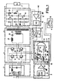
- Figure 1 shows a high voltage power supply according to the invention. It receives electrical energy from a single-phase network 1 and transforms it into high direct voltage intended to supply an X-ray tube 2. It comprises first means 3 of full-wave rectification and filtering of the single-phase voltage. An inverter 4 supplied by the rectifier 3 delivers in voltage boosting means 5. In one example, the inverter oscillates at several tens of kilohertz. Second rectifier means 6 rectify and filter the high alternating voltage supplied by the transformer 5. They deliver a high direct voltage in the tube 2. An important characteristic of the invention is that this chain 3 - 6 operates to periodically withdraw from the energy from the network 1 under the control of synchronization means 7. These synchronization means include means 8 for recognizing the phase of the network. They also include means 9 for varying the synchronization setting with respect to the phase of the network, or for varying the withdrawal times. The means 9 are in relation to commands 10 and 11 on which an operator can act.
- the power supply further comprises regulation means 12 which regulate the high voltage produced by the second rectifier 6 as a function of an ERV reference applied externally.
- the synchronization means 7 act on validation means 13 of the operation of the regulation means 12. In other words, when the synchronization means allow it, the regulated high voltage is discharged normally. When they no longer allow it, in particular during voltage dips in the single-phase signal from the network, the regulation chain is cut, the high voltage at the output is canceled.
- the first rectifying means 3 conventionally comprise double alternating rectifying means 14 in cascade with a low-pass filter 15.
- the inverter 4 conventionally comprises four power transistors mounted in pairs in cascade, 16 - 17 and 18 - 19, between the two outputs of the rectifier 3.
- the bases of the opposite diagonnaie transistors, 16-19 and 17-18, are connected together. They receive additional conduction orders via an inverter 20 of the validation means 13.
- the two cascades of transistors then function as PUSH - PULL type assemblies reversed from each other. Their midpoint, respectively 21 and 22 is connected to the voltage raising means 5.
- the means 5 comprise an oscillating circuit, with an inductance 23 and a capacity 24, tuned to a frequency slightly lower than the minimum frequency at which we waits to see the inverter vibrate 4.
- the natural frequency of this filter is 18 kilohertz.
- the inductance 23 represents the inductance 23 proper as well as the leakage inductance of a transformer 25 in series which is used for raising the voltage.
- the transformer 25 feeds into the second rectification means 6.
- These comprise two full-wave rectification circuits 26 and 27 respectively. They are each connected between a midpoint 28 of the transformer 25 and respectively one and the other of the ends of the secondary winding of this transformer.
- smoothing means comprising for example two capacitors 29 and 30 make it possible to filter the full-wave rectification of circuits 26 and 27 respectively.
- the high voltage then appears substantially flat. Capacities 29 and 30 are low because the rectified high alternating voltage is a high frequency voltage.
- the midpoint 35 of the rectifiers 26 - 27 is connected to ground. It allows the value of the high voltage produced to be divided by two, relative to it. The insulation constraints of the high voltage pads are then also halved.
- the interest of the oscillating circuit 23 - 24 lies in the sinusoidal aspect of the voltage which it produces.
- This sinusoidal voltage on the one hand crosses, more easily than a square signal of the same frequency, the transformer 25.
- the regular decrease of the current, as well as its regular growth, at each half-wave is favorable for a good destocking of the electronic charges stored at the time of saturation in the diodes of these rectifiers.
- This sinusoidal aspect is moreover favorable to the reduction of the reinjection of radio interference into the network 1.
- the regulation means 12 in fact comprise a frequency modulator 34 (VCO).
- VCO frequency modulator 34
- the oscillating circuit is slightly detuned by excess: the inverter vibrates for example at twenty kilohertzs while the oscillating circuit 23 -24 is tuned on 18 kilohertz.
- the oscillation frequency of the inverter is higher (for example 50 kilohertzs), the oscillating circuit is strongly detuned: it can pass less power.
- This frequency distribution is provided to minimize switching losses. Indeed at maximum high voltage, the oscillation frequency is the lowest, the switching losses are therefore the lowest. At minimum high voltage, the oscillation frequency is the highest, the switching losses are the highest; but it is not annoying since in this case the power required from the power supply is low.
- the regulation loop includes a comparator 31 which receives on a first input a signal coming from a divider bridge 32 - 33 (which measures the high voltage produced), and which receives on a second input a reference voltage VRE which represents the high voltage at which we want to operate the tube 2.
- the error signal produced by the comparator 31 is introduced into a frequency modulator 34. This produces for example a square signal at a frequency ultimately dependent on the reference voltage VRE.
- the square signal is applied at the same time as its complement on the corresponding bases of the transistors of the inverter 4.
- the synchronization means include means 8 for recognizing the phase of the sector signal.
- the means 8 comprise a full-wave rectifier 36 which flows into a comparator 37.
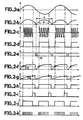
- the signal produced at the output of the means 8 is that which appears in FIG. 2e.
- the comparison voltage VC to which the full-wave rectified signal is compared is sufficiently low for the output signal from comparator 37 to have a rising edge 38 fairly close in time to the instant of zero crossing between two successive alternations.
- This phase identification signal is introduced into the means 9 to vary the timing.
- These include two RC circuits 38 - 39 and 40 - 41 respectively. The midpoints of these RC circuits are connected to first comparator inputs 42 and 43 respectively. Each comparator receives a threshold voltage at its second input: VS1 respectively and VS2.
- the circuits RC of the means 9 are each surmounted by a diode 47 or 48 to completely discharge the capacitors 39 or 41 at each change of half-wave.
- a diode 49 mounted in parallel at the output of comparator 37 promotes this discharge.
- Another special feature of RC circuits is that their time constant is adjustable.
- the resistors 38 and 40 can be adjusted by means of the graduated levers 10 and 11. By acting on these levers, the date of start-up as well as the date of shutdown of the inverter 4 is determined. duration.
- the validation circuit 13 comprises two logic gates AND respectively 45 and 46 receiving on a first of their inputs the signal from the AND gate 44. On their second input they receive the square signal, or its complementary, emanating from the modulator 34. These gates logic therefore deliver impulse signals comparable to that of the 2k diagram.
- the inverter operates. The X-ray tube is powered. Outside the durations at the bases of the inverter transistors are brought to zero, all these transistors are blocked, the X-ray tube is no longer supplied.
- Diagrams 2a to 2d respectively present the network signal, the rectified full-wave signal, the sinusoidal signal at the output of the inverter, and finally the filtered rectified high voltage signal applicable to the terminals of the X-ray tube.
- the oscillation frequency of the wavy signal is the same as the frequency of the signal delivered by logic gates 45 and 46.
- the duration a of operation of the inverter 4 is between dates where this phase is 40 ° and 140 °. .
- this way of acting has the effect of increasing the exposure time necessary for producing an X-ray photograph. In fact it is not.
- the peak value of the chopped DC voltage is of the order of 90% of the peak value of a half-wave rectified voltage, it can be established that the exposure times are almost identical.
- the images obtained in the invention are better since, during the entire installation, the supply voltage changes little. With a high voltage rectified double altemance (100 hertzs) the emitted spectrum borrows the whole range due to voltage dips.
Description
- La présente invention a pour objet une alimentation haute tension continue, notamment pour tube émetteur de rayons X. Elle peut néanmoins s'appliquer à d'autres domaines. Les alimentations concernées sont prévues pour être raccordées à un réseau général de distribution électrique.
- La plupart de ces alimentations comportent aujourd'hui des générateurs haute fréquence. Le secteur y est redressé, filtré, la tension continue obtenue est ondulée à haute fréquence par un onduleur, la tension ondulée est élevée par un transformateur élévateur, puis elle est redressée et filtrée. Ce type d'alimentation fonctionne parfaitement quand le réseau est triphasé. Par contre en monophasé quelques problèmes se posent. En effet, entre deux alternances il y a un creux de tension. Dans ce creux l'onduleur ne peut pas tirer de puissance du réseau. L'utilisation de filtre LC pour emmagasiner de l'énergie au sommet de la sinusoïde de façon à la restituer pendant ce creux est inapplicable pour les puissances de l'ordre de 30 à 100 kw. Les filtres deviennent énormes tant en dimension qu'en coût. Une autre solution très traditionnelle consiste a élever directement la tension secteur monophasé et à la redresser après élévation. Mais la haute tension redressée suit le réseau et chute complètement dans les creux de tension entre alternances. Le spectre des rayons X émis s'étend alors dans une gamme vaste. C'est une solution de plus en plus rejetée. Son emploi est même prohibé dans certain pays.
- La présente invention a pour objet de remédier aux inconvénients cités en proposant une alimentation où la haute tension est hachée. Elle n'est produite que pendant des durées courtes correspondant aux sommets des alternances du réseau monophasé. De cette manière on ne tire pas d'énergie du réseau lorsque celui-ci est à basse tension : le courant tube pendant ces arrêts est nul. Il n'y a alors pas de perte par effet Joule excessive dans le réseau.
- Une solution à ce problème a déjà été proposée dans le document FR-A 2 184 732. Cependant dans ce document les commandes d'inhibition de prélèvement d'énergie au réseau et le commande de la régulation haute tension sont couplées et interfèrent.
- Les problèmes ci-dessus sont résolus par les caractéristiques de la revendication 1.
- L'invention sera mieux comprise à la lecture de la description qui suit et à l'examen des figures qui l'ac- compagent. Elles ne sont données qu'à titre indicatif et nullement limitatif de la portée de l'invention. Elles représentent :
- - figure 1, une alimentation conforme à l'invention ;
- - figures 2a à 2k, des diagrammes temporels de signaux intervenant dans l'alimentation de l'invention.
- La figure 1 montre une alimentation haute tension conforme à l'invention. Elle reçoit l'énergie électrique d'un réseau monophasé 1 et la transforme en haute tension continue destinée à alimenter un tube 2 à rayons X. Elle comporte des premiers moyens 3 de redressement double alternance et de filtrage de la tension monophasée. Un onduleur 4 alimenté par le redresseur 3 débite dans des moyens élévateur de tensions 5. Dans un exemple, l'onduleur oscille à plusieurs dizaines de kilohertzs. Des deuxièmes moyens redresseurs 6 redressent et filtrent la haute tension alternative fournie par le transformateur 5. Ils débitent une haute tension continue dans le tube 2. Une caractéristique importante de l'invention est que cette chaine 3 - 6 fonctionne pour soutirer périodiquement de l'énergie du réseau 1 sous le pilotage de moyens 7 de synchronisation. Ces moyens de synchronisation comportent des moyens 8 pour reconnaître la phase du réseau. Ils comportent également des moyens 9 pour faire varier le calage de synchronisation par rapport à la phase du réseau, ou pour faire varier les durées de soutirage. Les moyens 9 sont en relation avec des commandes 10 et 11 sur lesquelles peut agir un opérateur.
- Dans l'exemple représenté l'alimentation comporte en outre des moyens de régulation 12 qui règlent la haute tension produite par le deuxième redresseur 6 en fonction d'une référence VRE appliquée extérieurement. Dans une réalisation préférée les moyens de synchronisation 7 agissent sur des moyens de validation 13 du fonctionnement des moyens 12 de régulation. Autrement dit, lorsque les moyens de synchronisation le permettent, la haute tension régulée est débitée normalement. Lorsqu'ils ne le permettent plus, en particulier pendant les creux de tension du signal monophasé du réseau, la chaine de régulation est coupée, la haute tension en sortie s'annule.
- Les premiers moyens de redressement 3 comportent classiquement des moyens de redressement double alternance 14 en cascade avec un filtre passe-bas 15. L'onduleur 4 comporte classiquement quatre transistors de puissance montés deux à deux en cascade, 16 - 17 et 18 - 19, entre les deux sorties du redresseur 3. Les bases des transistors opposés en diagonnaie, 16-19 et 17-18, sont connectées ensemble. Elles reçoivent des ordres complémentaires de mise en conduction par l'intermédiaire d'un inverseur 20 des moyens 13 de validation. Les deux cascades de transistors fonctionnent alors comme des montages de type PUSH - PULL inversés l'un de l'autre. Leur point milieu, respectivement 21 et 22 est relié aux moyens élévateur de tension 5. Ici les moyens 5 comportent un circuit oscillant, avec une inductance 23 et une capacité 24, accordé sur une fréquence légèrement inférieure à la fréquence minimum à laquelle on s'attend à voir vibrer l'onduleur 4. Dans un exemple la fréquence propre de ce filtre vaut 18 kilohertzs. L'inductance 23 représente l'inductance 23 proprement dite ainsi que l'inductance de fuite d'un transformateur 25 en série qui sert à l'élévation de tension.
- Le transformateur 25 débite dans les deuxièmes moyens de redressement 6. Ceux-ci comportent deux circuits de redressement double alternance respectivement 26 et 27. Ils sont chacun raccordés entre un point milieu 28 du transformateur 25 et respectivement l'une et l'autre des extrémités de l'enroulement secondaire de ce transformateur. Des moyens de lissage comportant par exemple deux capacités 29 et 30 permettent de filtrer le redressement double alternance respectivement des circuits 26 et 27. La haute tension apparaît alors sensiblement plate. Les capacités 29 et 30 sont faibles du fait que la haute tension alternative redressée est une tension haute fréquence. Le point milieu 35 des redresseurs 26 - 27 est relié à la masse. Il permet de diviser par deux, par rapport à celle-ci, la valeur de la haute tension produite. Les contraintes d'isolement des plots de la haute tension sont alors également divisées par deux.
- L'intérêt du circuit oscillant 23 - 24 réside dans l'aspect sinusoïdal de la tension qu'il produit. Cette tension sinusoïdale d'une part franchit, plus aisément qu'un signal carré de même fréquence, le transformateur 25. D'autre part lors du redressement dans les redresseurs 26 et 27, la décroissance régulière du courant, ainsi que sa croissance régulière, à chaque demi-alternance est favorable à un bon déstockage des charges électroniques stockées au moment de la saturation dans les diodes de ces redresseurs. Cet aspect sinusoïdal est par ailleurs favorable à la diminution de la réinjection de parasites radioélectriques dans le réseau 1.
- On verra plus loin que la régulation de l'alimentation est faite par modulation de fréquence. Les moyens de régulation 12 comportent en effet un modulateur de fréquence 34 (VCO). A haute tension maximum le circuit oscillant est légèrement désaccordé par excès : l'onduleur vibre par exemple à vingt kilohertzs alors que le circuit oscillant 23 -24 est accordé sur 18 kilohertzs. A haute tension minimum la fréquence d'oscillation de l'onduleur est plus élevée (par exemple 50 kilohertzs), le circuit oscillant est fortement désaccordé : il peut passer moins de puissance. Cette répartition en fréquence est prévue pour minimiser les pertes par commutation. En effet à haute tension maximum, la fréquence d'oscillation est la plus faible, les pertes par commutation sont donc les plus faibles. A haute tension minimum, la fréquence d'oscillation est la plus élevée, les pertes par commutation sont les plus fortes ; mais ce n'est pas génant puisque dans ce cas la puissance demandée à l'alimentation est faible.
- La boucle de régulation comporte un comparateur 31 qui reçoit sur une première entrée un signal provenant d'un pont diviseur 32 - 33 (qui mesure la haute tension produite), et qui reçoit sur une deuxième entrée une tension de référence VRE qui représente la haute tension à laquelle on veut faire fonctionner le tube 2. Le signal d'erreur produit par le comparateur 31 est introduit dans un modulateur de fréquence 34. Celui-ci produit par exemple un signal carré à une fréquence dépendant en définitive de la tension de référence VRE. Le signal carré est appliqué en même temps que son complémentaire sur les bases correspondantes des transistors de l'onduleur 4.
- Les moyens de synchronisation comportent des moyens 8 de reconnaître la phase du signal secteur. Les moyens 8 comportent un redresseur double alternance 36 qui débite dans un comparateur 37. Le signal produit en sortie des moyens 8 est celui qui apparaît sur la figure 2e. La tension de comparaison VC à laquelle est comparé le signal redressé double alternance est suffisamment faible pour que le signal de sortie du comparateur 37 présente un front de montée 38 assez proche dans le temps de l'instant de passage à zéro entre deux alternances successives. Ce signal de repérage de phase est introduit dans les moyens 9 pour faire varier le calage. Ceux-ci comportent deux circuits RC respectivement 38 - 39 et 40 - 41. Les points milieu de ces circuits RC sont reliés à des premières entrées de comparateurs respectivement 42 et 43. Chaque comparateur reçoit sur sa deuxième entrée une tension de seuil : respectivement VS1 et VS2. Ces deux tensions peuvent être égales mais ce n'est pas une obligation. Le front de montée 38 du signal émanant du comparateur 37 ne se transmet pas immédiatement aux capacités 39 ou 41. Celles-ci ne sont chargées qu'au bout d'un temps dépendant de la constante de temps de leur circuits RC. Les diagrammes 2f et 2g montrent comment évoluent les potentiels aux bornes des capacités. Dans un exemple la constante de temps du circuit 38 - 39 est inférieure à la constante de temps du circuit 40 - 41. Dans cet exemple les seuils VS1 et VS2 étant égaux le comparateur 42 bascule avant le comparateur 43. Ceci est visible sur les diagrammes 2h et 2i. En reliant les sorties de ces comparateurs aux entrées d'une porte logique ET 44 (en ayant au préalable inversé la sortie du comparateur 43) on dispose en sortie de cette porte 44 d'un crénaux logique actif entre les dates où les comparateurs 42 et 43 ont basculé. Ceci apparaît sur le diagramme 2j.
- Les circuits RC des moyens 9 sont chacun surmontés d'une diode 47 ou 48 pour décharger complètement les capacités 39 ou 41 à chaque changement de demi-alternance. Une diode 49 montée en parallèle à la sortie du comparateur 37 favorise cette décharge. Une autre particularité des circuits RC est que leur constante de temps est réglable. Par exemple les résistances 38 et 40 peuvent être réglées aux moyens des manettes graduées 10 et 11. En agissant sur ces manettes on détermine la date de mise en fonctionnement ainsi que la date d'arrêt de l'onduleur 4. On peut donc modifier la durée.
- Le circuit de validation 13 comporte deux portes logiques ET respectivement 45 et 46 recevant sur une première de leurs entrées le signal de la porte ET 44. Sur leur deuxième entrée elles reçoivent le signal carré, ou son complémentaire, émanant du modulateur 34. Ces portes logiques délivrent donc des signaux impulsionnels comparables à celui du diagramme 2k. Pendant les durées actives, de durée a dans une durée 12 de demi-alternance, l'onduleur fonctionne. Le tube à rayons X est alimenté. En dehors des durées a les bases des transistors de l'onduleur sont portées à zéro, tous ces transistors sont bloqués, le tube à rayons X n'est plus alimenté.
- Les diagrammes 2a à 2d présentent respectivement le signal du réseau, le signal redressé double alternance, le signal sinusoïdal en sortie de l'onduleur, et enfin le signal haute tension redressé filtré applicable aux bornes du tube à rayons X. La fréquence d'oscillation du signal ondulé est la même que la fréquence du signal délivré par les portes logique 45 et 46.
- D'une manière préférée, par rapport à une demi-alternance correspondant à une rotation de phase de 180° la durée a de mise en fonctionnement de l'on- dudeur 4 est comprise entre des dates où cette phase vaut 40° et 140°. On pourrait penser que cette manière d'agir a pour effet d'augmenter le temps de pose nécessaire à la réalisation d'un cliché radiographique. En fait il n'en est rien. Pour la durée de fonctionnement a évoquée, si la valeur crête de la tension continue hachée est de l'ordre de 90 % de la valeur crête d'une tension redressée double alternance, on peut établir que les temps de pose sont quasiment identiques. Par ailleurs les images obtenues dans l'invention sont meilleures puisque pendant toute la pose la tension d'alimentation évolue peu. Avec une haute tension redressée double al- temance (100 hertzs) le spectre émis emprunte toute la gamme du fait des creux de tension.
- Par comparaison à une alimentation classique où la tension continue ne serait pas hachée les temps de pose sont augmentés dans le rapport b/a. Or ces solutions classiques ne sont que théoriques en monophasé du fait des capacités et des inductances trop importantes qu'elles requièrent. On a pu établir en particulier que les éléments de filtrage (29 ou 30) peuvent être réduits dans un rapport 4 alors que le temps de pose n'est même pas doublé. Il est possible par ailleurs d'éffectuer des réglages de telle manière qu'à haute tension faible le rapport cyclique a/b soit plus élevé. On agit alors sur les manettes 10 et 11. Des mesures comparatives ont été effectuées. Elles ont permis d'établir que le courant crête absorbé au réseau 1 était bien inférieur dans l'invention à celui mesuré avec un générateur à haute tension continue permanente. Ceci est dû essentiellement au fait que la charge 2 ne soutire pas de courant quand la tension sur le réseau est faible : c'est-à-dire pendant les creux de tension. Le rendement de consommation est bien supérieur dans le cas de l'invention. En particulier l'énergie électrique prélevée sous forme d'un courant est dissipé en partie par le réseau lui-même car celui-ci qui n'est pas parfaitement conducteur. De ce point de vue, plus la résistance interne du réseau est élevée plus la comparaison est favorable à l'invention.
Claims (5)
Applications Claiming Priority (2)
| Application Number | Priority Date | Filing Date | Title |
|---|---|---|---|
| FR8501971A FR2577373B1 (fr) | 1985-02-12 | 1985-02-12 | Alimentation haute tension continue, notamment pour emetteur de rayons x |
| FR8501971 | 1985-02-12 |
Publications (2)
| Publication Number | Publication Date |
|---|---|
| EP0192553A1 EP0192553A1 (fr) | 1986-08-27 |
| EP0192553B1 true EP0192553B1 (fr) | 1990-04-25 |
Family
ID=9316177
Family Applications (1)
| Application Number | Title | Priority Date | Filing Date |
|---|---|---|---|
| EP86400265A Expired - Lifetime EP0192553B1 (fr) | 1985-02-12 | 1986-02-07 | Alimentation haute tension continue, notamment pour tube émetteur de rayons X |
Country Status (4)
| Country | Link |
|---|---|
| US (1) | US4680693A (fr) |
| EP (1) | EP0192553B1 (fr) |
| DE (1) | DE3670734D1 (fr) |
| FR (1) | FR2577373B1 (fr) |
Families Citing this family (13)
| Publication number | Priority date | Publication date | Assignee | Title |
|---|---|---|---|---|
| US4727469A (en) * | 1987-03-23 | 1988-02-23 | Reliance Comm/Tec Corporation | Control for a series resonant power converter |
| US4797803A (en) * | 1987-12-23 | 1989-01-10 | Dci Technology | Switching power supply VCO |
| US5189602A (en) * | 1989-05-12 | 1993-02-23 | General Electric Cgr S.A. | High-voltage generator with selective half-bridge and full-bridge operation |
| DE3928809A1 (de) * | 1989-08-31 | 1991-03-07 | Philips Patentverwaltung | Schaltungsanordnung zum speisen einer last |
| FR2665999B1 (fr) * | 1990-08-14 | 1994-01-28 | General Electric Cgr Sa | Dispositif d'obtention d'une tension continue reglable. |
| FR2666000B1 (fr) * | 1990-08-14 | 1996-09-13 | Gen Electric Cgr | Dispositif d'alimentation et de regulation en courant d'un filament de cathode d'un tube radiogene. |
| FR2672166B1 (fr) * | 1991-01-25 | 1995-04-28 | Gen Electric Cgr | Dispositif pour obtenir une tension continue a faible ondulation residuelle. |
| US5267138A (en) * | 1992-03-23 | 1993-11-30 | Creos International Ltd. | Driving and clamping power regulation technique for continuous, in-phase, full-duration, switch-mode resonant converter power supply |
| US6195272B1 (en) | 2000-03-16 | 2001-02-27 | Joseph E. Pascente | Pulsed high voltage power supply radiography system having a one to one correspondence between low voltage input pulses and high voltage output pulses |
| US6181580B1 (en) * | 2000-05-25 | 2001-01-30 | General Electric Company | Single-supply gridding and biasing circuitry |
| DE10228336C1 (de) * | 2002-06-25 | 2003-11-27 | Siemens Ag | Schaltungsanordnung und Verfahren zur Erzeugung einer Röntgenröhrenspannung, sowie Röntgengenerator und Röntgeneinrichtung |
| JP4392746B2 (ja) * | 2003-05-23 | 2010-01-06 | 株式会社日立メディコ | X線高電圧装置 |
| EA016999B1 (ru) * | 2009-06-24 | 2012-09-28 | Анатолий Яковлевич КАРТЕЛЕВ | Устройство для электрогидравлического воздействия на призабойную зону скважины |
Family Cites Families (10)
| Publication number | Priority date | Publication date | Assignee | Title |
|---|---|---|---|---|
| US3539812A (en) * | 1968-01-23 | 1970-11-10 | Westinghouse Electric Corp | Polyphase power supply for x-ray apparatus with means for preventing saturation in the transformer |
| DE2223371B2 (de) * | 1972-05-12 | 1976-09-02 | Siemens AG, 1000 Berlin und 8000 München | Roentgendiagnostikapparat mit einer regeleinrichtung fuer die roentgenroehrenspannung |
| JPS58959Y2 (ja) * | 1977-05-18 | 1983-01-08 | 株式会社東芝 | X線発生装置 |
| GB1602613A (en) * | 1977-06-24 | 1981-11-11 | Chloride Group Ltd | Converters |
| DE2802424A1 (de) * | 1978-01-20 | 1979-07-26 | Siemens Ag | Roentgendiagnostikgenerator mit einem seinen hochspannungstransformator speisenden wechselrichter |
| DE2917594A1 (de) * | 1979-04-30 | 1980-11-13 | Siemens Ag | Ein- oder zweipuls-roentgendiagnostikgenerator |
| US4301498A (en) * | 1979-10-31 | 1981-11-17 | Gould Advance Limited | Voltage converter apparatus having output regulating means |
| JPS5889075A (ja) * | 1981-11-24 | 1983-05-27 | Hitachi Ltd | 共振形スイツチング電源装置 |
| US4504895A (en) * | 1982-11-03 | 1985-03-12 | General Electric Company | Regulated dc-dc converter using a resonating transformer |
| IL73674A0 (en) * | 1983-12-22 | 1985-02-28 | Gen Electric | Inverter driver for x-ray generator |
-
1985
- 1985-02-12 FR FR8501971A patent/FR2577373B1/fr not_active Expired - Lifetime
-
1986
- 1986-02-07 DE DE8686400265T patent/DE3670734D1/de not_active Expired - Lifetime
- 1986-02-07 EP EP86400265A patent/EP0192553B1/fr not_active Expired - Lifetime
- 1986-02-10 US US06/827,725 patent/US4680693A/en not_active Expired - Fee Related
Also Published As
| Publication number | Publication date |
|---|---|
| DE3670734D1 (de) | 1990-05-31 |
| FR2577373A1 (fr) | 1986-08-14 |
| EP0192553A1 (fr) | 1986-08-27 |
| FR2577373B1 (fr) | 1995-02-17 |
| US4680693A (en) | 1987-07-14 |
Similar Documents
| Publication | Publication Date | Title |
|---|---|---|
| EP0192553B1 (fr) | Alimentation haute tension continue, notamment pour tube émetteur de rayons X | |
| FR2541531A1 (fr) | Procede pour creer un courant alternatif a partir d'un courant continu | |
| FR2745446A1 (fr) | Circuit integre de correction de facteur de puissance | |
| EP0720281B1 (fr) | Dispositif électronique de conversion de l'énergie électrique | |
| EP0193435B1 (fr) | Circuit de commande d'alimentation à découpage à démarrage automatique | |
| FR3004870A1 (fr) | Procede et dispositif de commande d'un convertisseur multiphase courant continu-courant continu a resonance, et convertisseur multiphase correspondant | |
| CA1237472A (fr) | Convertisseur de frequence statique de puissance | |
| FR2738417A1 (fr) | Convertisseur de tension continue a commutation douce | |
| EP1275196B1 (fr) | Moteur a angle d'avance de phase | |
| FR2742277A1 (fr) | Dispositif d'alimentation a decoupage | |
| EP0329571B1 (fr) | Dispositif de surveillance de démagnétisation pour alimentation à découpage à régulation primaire et secondaire | |
| FR2772154A1 (fr) | Circuit de commande pour la correction du facteur de puissance | |
| EP0193436A1 (fr) | Circuit de commande d'alimentation à découpage à démarrage progressif | |
| FR2508736A1 (fr) | Systeme d'alimentation | |
| FR2783370A1 (fr) | Dispositif d'alimentation a onduleur dont la puissance delivree est controlee | |
| FR2610461A1 (fr) | Convertisseur electronique courant alternatif-courant continu-courant alternatif | |
| FR2605168A1 (fr) | Circuit de commande en mode veille d'une alimentation a decoupage | |
| EP0176413B1 (fr) | Convertisseur de courant continu en courant continu à découpage | |
| FR2539563A1 (fr) | Source de puissance alternative haute frequence | |
| FR2768241A1 (fr) | Dispositif et procede de regulation a commande optimale d'un convertisseur a transistors | |
| EP1444768B1 (fr) | Procede et dispositif de transformation d'une tension continue, et utilisation du dispositif | |
| CA2170317C (fr) | Procede de commande pour courant electrique bidirectionnel et onduleur de tension a commutation douce | |
| FR2675000A1 (fr) | Procede et dispositif pour attenuer l'effet du radioparasitage par conduction sur le reseau alternatif polyphase. | |
| EP0928057B1 (fr) | Interrupteur haute tension realisé à partir de cellules resonantes connectées en serie | |
| EP1335483A1 (fr) | Circuit secondaire de convertisseur comportant au moins une sortie auxiliaire |
Legal Events
| Date | Code | Title | Description |
|---|---|---|---|
| PUAI | Public reference made under article 153(3) epc to a published international application that has entered the european phase |
Free format text: ORIGINAL CODE: 0009012 |
|
| AK | Designated contracting states |
Kind code of ref document: A1 Designated state(s): BE DE GB IT LU NL |
|
| 17P | Request for examination filed |
Effective date: 19860919 |
|
| 17Q | First examination report despatched |
Effective date: 19880108 |
|
| RAP1 | Party data changed (applicant data changed or rights of an application transferred) |
Owner name: GENERAL ELECTRIC CGR SA. |
|
| GRAA | (expected) grant |
Free format text: ORIGINAL CODE: 0009210 |
|
| AK | Designated contracting states |
Kind code of ref document: B1 Designated state(s): BE DE GB IT LU NL |
|
| ITF | It: translation for a ep patent filed |
Owner name: JACOBACCI & PERANI S.P.A. |
|
| GBT | Gb: translation of ep patent filed (gb section 77(6)(a)/1977) | ||
| REF | Corresponds to: |
Ref document number: 3670734 Country of ref document: DE Date of ref document: 19900531 |
|
| PLBE | No opposition filed within time limit |
Free format text: ORIGINAL CODE: 0009261 |
|
| STAA | Information on the status of an ep patent application or granted ep patent |
Free format text: STATUS: NO OPPOSITION FILED WITHIN TIME LIMIT |
|
| PG25 | Lapsed in a contracting state [announced via postgrant information from national office to epo] |
Ref country code: LU Free format text: LAPSE BECAUSE OF NON-PAYMENT OF DUE FEES Effective date: 19910228 |
|
| 26N | No opposition filed | ||
| PGFP | Annual fee paid to national office [announced via postgrant information from national office to epo] |
Ref country code: GB Payment date: 19920124 Year of fee payment: 7 |
|
| PGFP | Annual fee paid to national office [announced via postgrant information from national office to epo] |
Ref country code: BE Payment date: 19920204 Year of fee payment: 7 |
|
| ITTA | It: last paid annual fee | ||
| PG25 | Lapsed in a contracting state [announced via postgrant information from national office to epo] |
Ref country code: GB Effective date: 19930207 |
|
| PG25 | Lapsed in a contracting state [announced via postgrant information from national office to epo] |
Ref country code: BE Effective date: 19930228 |
|
| PGFP | Annual fee paid to national office [announced via postgrant information from national office to epo] |
Ref country code: NL Payment date: 19930228 Year of fee payment: 8 |
|
| BERE | Be: lapsed |
Owner name: S.A. GENERAL ELECTRIC CGR Effective date: 19930228 |
|
| GBPC | Gb: european patent ceased through non-payment of renewal fee |
Effective date: 19930207 |
|
| PG25 | Lapsed in a contracting state [announced via postgrant information from national office to epo] |
Ref country code: NL Effective date: 19940901 |
|
| NLV4 | Nl: lapsed or anulled due to non-payment of the annual fee | ||
| PG25 | Lapsed in a contracting state [announced via postgrant information from national office to epo] |
Ref country code: IT Free format text: LAPSE BECAUSE OF NON-PAYMENT OF DUE FEES;WARNING: LAPSES OF ITALIAN PATENTS WITH EFFECTIVE DATE BEFORE 2007 MAY HAVE OCCURRED AT ANY TIME BEFORE 2007. THE CORRECT EFFECTIVE DATE MAY BE DIFFERENT FROM THE ONE RECORDED. Effective date: 20050207 |
|
| PGFP | Annual fee paid to national office [announced via postgrant information from national office to epo] |
Ref country code: DE Payment date: 20050331 Year of fee payment: 20 |