EP0195203A2 - Display controller - Google Patents
Display controller Download PDFInfo
- Publication number
- EP0195203A2 EP0195203A2 EP86101119A EP86101119A EP0195203A2 EP 0195203 A2 EP0195203 A2 EP 0195203A2 EP 86101119 A EP86101119 A EP 86101119A EP 86101119 A EP86101119 A EP 86101119A EP 0195203 A2 EP0195203 A2 EP 0195203A2
- Authority
- EP
- European Patent Office
- Prior art keywords
- display
- data
- signal
- display unit
- address
- Prior art date
- Legal status (The legal status is an assumption and is not a legal conclusion. Google has not performed a legal analysis and makes no representation as to the accuracy of the status listed.)
- Granted
Links
Images


Classifications
-
- G—PHYSICS
- G06—COMPUTING; CALCULATING OR COUNTING
- G06F—ELECTRIC DIGITAL DATA PROCESSING
- G06F3/00—Input arrangements for transferring data to be processed into a form capable of being handled by the computer; Output arrangements for transferring data from processing unit to output unit, e.g. interface arrangements
- G06F3/14—Digital output to display device ; Cooperation and interconnection of the display device with other functional units
- G06F3/147—Digital output to display device ; Cooperation and interconnection of the display device with other functional units using display panels
- G06F3/1475—Digital output to display device ; Cooperation and interconnection of the display device with other functional units using display panels with conversion of CRT control signals to flat panel control signals, e.g. adapting the palette memory
-
- G—PHYSICS
- G09—EDUCATION; CRYPTOGRAPHY; DISPLAY; ADVERTISING; SEALS
- G09G—ARRANGEMENTS OR CIRCUITS FOR CONTROL OF INDICATING DEVICES USING STATIC MEANS TO PRESENT VARIABLE INFORMATION
- G09G3/00—Control arrangements or circuits, of interest only in connection with visual indicators other than cathode-ray tubes
- G09G3/20—Control arrangements or circuits, of interest only in connection with visual indicators other than cathode-ray tubes for presentation of an assembly of a number of characters, e.g. a page, by composing the assembly by combination of individual elements arranged in a matrix no fixed position being assigned to or needed to be assigned to the individual characters or partial characters
- G09G3/34—Control arrangements or circuits, of interest only in connection with visual indicators other than cathode-ray tubes for presentation of an assembly of a number of characters, e.g. a page, by composing the assembly by combination of individual elements arranged in a matrix no fixed position being assigned to or needed to be assigned to the individual characters or partial characters by control of light from an independent source
- G09G3/36—Control arrangements or circuits, of interest only in connection with visual indicators other than cathode-ray tubes for presentation of an assembly of a number of characters, e.g. a page, by composing the assembly by combination of individual elements arranged in a matrix no fixed position being assigned to or needed to be assigned to the individual characters or partial characters by control of light from an independent source using liquid crystals
- G09G3/3611—Control of matrices with row and column drivers
- G09G3/3622—Control of matrices with row and column drivers using a passive matrix
- G09G3/3644—Control of matrices with row and column drivers using a passive matrix with the matrix divided into sections
-
- G—PHYSICS
- G09—EDUCATION; CRYPTOGRAPHY; DISPLAY; ADVERTISING; SEALS
- G09G—ARRANGEMENTS OR CIRCUITS FOR CONTROL OF INDICATING DEVICES USING STATIC MEANS TO PRESENT VARIABLE INFORMATION
- G09G3/00—Control arrangements or circuits, of interest only in connection with visual indicators other than cathode-ray tubes
- G09G3/20—Control arrangements or circuits, of interest only in connection with visual indicators other than cathode-ray tubes for presentation of an assembly of a number of characters, e.g. a page, by composing the assembly by combination of individual elements arranged in a matrix no fixed position being assigned to or needed to be assigned to the individual characters or partial characters
- G09G3/34—Control arrangements or circuits, of interest only in connection with visual indicators other than cathode-ray tubes for presentation of an assembly of a number of characters, e.g. a page, by composing the assembly by combination of individual elements arranged in a matrix no fixed position being assigned to or needed to be assigned to the individual characters or partial characters by control of light from an independent source
- G09G3/36—Control arrangements or circuits, of interest only in connection with visual indicators other than cathode-ray tubes for presentation of an assembly of a number of characters, e.g. a page, by composing the assembly by combination of individual elements arranged in a matrix no fixed position being assigned to or needed to be assigned to the individual characters or partial characters by control of light from an independent source using liquid crystals
- G09G3/3611—Control of matrices with row and column drivers
- G09G3/3685—Details of drivers for data electrodes
-
- G—PHYSICS
- G09—EDUCATION; CRYPTOGRAPHY; DISPLAY; ADVERTISING; SEALS
- G09G—ARRANGEMENTS OR CIRCUITS FOR CONTROL OF INDICATING DEVICES USING STATIC MEANS TO PRESENT VARIABLE INFORMATION
- G09G5/00—Control arrangements or circuits for visual indicators common to cathode-ray tube indicators and other visual indicators
- G09G5/22—Control arrangements or circuits for visual indicators common to cathode-ray tube indicators and other visual indicators characterised by the display of characters or indicia using display control signals derived from coded signals representing the characters or indicia, e.g. with a character-code memory
- G09G5/222—Control of the character-code memory
-
- G—PHYSICS
- G09—EDUCATION; CRYPTOGRAPHY; DISPLAY; ADVERTISING; SEALS
- G09G—ARRANGEMENTS OR CIRCUITS FOR CONTROL OF INDICATING DEVICES USING STATIC MEANS TO PRESENT VARIABLE INFORMATION
- G09G2360/00—Aspects of the architecture of display systems
- G09G2360/04—Display device controller operating with a plurality of display units
-
- G—PHYSICS
- G09—EDUCATION; CRYPTOGRAPHY; DISPLAY; ADVERTISING; SEALS
- G09G—ARRANGEMENTS OR CIRCUITS FOR CONTROL OF INDICATING DEVICES USING STATIC MEANS TO PRESENT VARIABLE INFORMATION
- G09G3/00—Control arrangements or circuits, of interest only in connection with visual indicators other than cathode-ray tubes
- G09G3/20—Control arrangements or circuits, of interest only in connection with visual indicators other than cathode-ray tubes for presentation of an assembly of a number of characters, e.g. a page, by composing the assembly by combination of individual elements arranged in a matrix no fixed position being assigned to or needed to be assigned to the individual characters or partial characters
- G09G3/2007—Display of intermediate tones
- G09G3/2018—Display of intermediate tones by time modulation using two or more time intervals
Landscapes
- Engineering & Computer Science (AREA)
- Theoretical Computer Science (AREA)
- Physics & Mathematics (AREA)
- General Physics & Mathematics (AREA)
- Computer Hardware Design (AREA)
- Crystallography & Structural Chemistry (AREA)
- Chemical & Material Sciences (AREA)
- Human Computer Interaction (AREA)
- General Engineering & Computer Science (AREA)
- Controls And Circuits For Display Device (AREA)
- Liquid Crystal Display Device Control (AREA)
- Control Of Indicators Other Than Cathode Ray Tubes (AREA)
- Liquid Crystal (AREA)
- Digital Computer Display Output (AREA)
Abstract
Description
- This invention relates to a display controller capable of driving either of a CRT display unit and a liquid crystal display unit.
- A visual display unit is an indispensable terminal device for a computer system such as a personal computer and an office computer. Until recently, CRT (cathode-ray tube) display units were used in most of the computer systems as such terminal devices, however, the recent advance in the liquid crystal display technology made it possible to use liquid crystal display units as the terminal devices of computer systems particularly of portable type.
- There has been proposed a display controller formed in an LSI device which can drive a display unit in accordance with commands fed from a central processing unit connected thereto. For example, a pPD3301 manufactured by Nippon Electric Co., Ltd. and an HD46505 manufactured by Hitachi, Ltd. can control CRT display units, and a yPD7203OG manufactured by Nippon Electric Co., Ltd. and an HD61830 manufactured by Hitachi, Ltd. can control liquid crystal display units.
- A commercially available liquid crystal display unit is generally composed of two (upper and lower) screens which are independently driven, while a CRT display unit can be driven as one screen. Thus, a CRT display unit and a liquid crystal display unit must be driven in the different manners from each other. Also the manner of reading data from the video memory for a CRT display unit is different from that for a liquid crystal display unit. For this reason, each of the aforesaid conventional display controllers is designed so as to drive only one of the two kinds of display units. As a result, when it is desired to change the display unit used to another display unit of a different type, not only the display controller but also the control program therefor must be changed.
- It is therefore an object of the present invention to provide a display controller which can drive either of a CRT display unit and a liquid crystal display unit.
- It is another object of the invention to provide a display controller which can be controlled by the same program executed by a central processing unit irrespective of the kind of the display unit connected thereto.
- According to an aspect of the present invention, there is provided a display controller comprising a display controller capable of selectively driving one of first and second display units, the first display unit having a display screen comprised of a scanning-type screen which provides M rows of N columns of display positions thereon, the second display unit having a display screen constituted by upper and lower scanning-type screens each of which provides P rows of Q columns of display positions thereon, the display controller being further connected to memory means having a plurality of addresses each for storing display data relating to an image to be displayed in a respective one of the display positions of the selected display unit, the display controller comprising display unit designating means for designating one of the first and second display units, the designation means outputting a first designation signal when the first display unit is selected, and outputting a second designation signal when the second display unit is selected; timing signal generating means responsive to the first designation signal for generating synchronization signals to be supplied to the first display unit for scanning the screen thereof, the timing signal generating means being further responsive to the second designation signal to generate synchronization signals to be supplied to the second display unit for scanning the upper and lower screens thereof; address data generating means responsive to the first designation signal for generating a first series of address data representative of the addresses of the memory means to sequentially output the generated address data to the memory means in accordance with the scanning of the display screen of the first display unit, the address data generating means being further responsive to the second designation signal for generating a second series of address data representative of those of the addresses of the memory means corresponding to the upper screen and a third series of address data representative of those of the addresses of the memory means corresponding to the lower screen, the address data generating means alternately outputting each of the second series of address data and each of the third series of address data to the memory means in accordance with the scannings of the upper and lower screens; and display signal generating means responsive to the first designation signal for generating a first display signal to be supplied to the first display unit based on data read from the memory means in accordance with the first series of address data, the display signal generating means being further responsive to the second designation signal to generate second and third display signals to be supplied to the second display unit based on data read from the memory means in accordance with the second and third series of address data, the second and third display signals being used to display images on the upper and lower screens, respectively.
- Examples of the present invention will now be described with reference to the accompanying drawings, in which:-
- Fig. 1 is a block diagram of a display system in which a
display controller 1 provided in accordance with the present invention is used; - Fig. 2 is an illustration showing the
video memory 4 of the display system of Fig. 1; - Fig. 3 is an illustration showing data to be written into the
video memory 4 of Fig. 2; - Fig. 4 is an illustration showing the display screen;
- Fig. 5 is a block diagram of the liquid
crystal display unit 3 of the display system of Fig. 1; - Fig. 6 is a block diagram of the
display controller 1 of the display system of Fig. 1; - Fig. 7 is a block diagram of the
address generating circuit 21 of thedisplay controller 1 of Fig. 6; - Fig. 8 is a timing chart showing the operation of the gray-
scale display circuit 37 of thedisplay controller 1 of Fig. 6; - Fig. 9 is a block diagram of one example of the gray-
scale display circuit 37 of thedisplay controller 1 of Fig. 6; - Fig. 10 is an illustration showing the waveforms of the clock pulses ø0 to 02; 1
- Figs. 11 to 14 are timing charts of the various signals appearing in the
display controller 1 when theCRT display unit 2 is connected thereto; and - Figs. 15 to 19 are timing charts of the various signals appearing in the
display controller 1 when theLCD 3 is connected thereto. - Fig. 1 shows the structure of a display system to which a
display controller 1 provided in accordance with one embodiment of the invention is applied. Thedisplay controller 1 is of a character display type and effects, in accordance with data stored in avideo memory 4, display of characters using 640 x 192 display dots provided on a screen of aCRT display unit 2 or a liquid crystal display unit (hereinafter referred to as "LCD") 3. Thedisplay controller 1 drives either of theCRT display unit 2 and theLCD 3 but does not drive both of them at the same time. - The display system shown in Fig. 1 will now be fully described.
- Shown at 5 is a central processing unit (CPU) which is connected to a
memory 6 including a ROM for storing programs to be executed by theCPU 5 and a ROM for storing data. TheCPU 5 stores display data into thevideo memory 4 which comprises, as shown in Fig. 2, two areas Eo and E1 of the same storage capacity. The area Eo is selected when a "0" signal is supplied to a terminal CS of thevideo memory 4, while the area E1 is selected when a "1" signal is supplied to the terminal CS. An address in each of the areas Eo and E1 is designated by an address data supplied to an address terminal AD of thememory 4, and read/write of data is performed through a data terminal DT thereof. Thememory 4 also comprises a read/write control terminal R/W. - The construction of the
video memory 4 and the relation between the addresses of thememory 4 and display positions of characters on the screen will be described. The display data is formed on a two-byte unit basis, and a character to be displayed is represented by two bytes. Fig. 3 shows the two bytes forming a unit of the display data, wherein the first byte contains a character code for designating a character to be displayed and the second byte contains a foreground color code FCA in the lower four bits and a background color code BCA in the higher four bits. In this case, the color code FCA designates a color of the character and the color code BCA designates a color of the background of the character. The character code CRC and the color codes FCA and BCA for a character are stored in the same addresses of the areas Eo and E1. For example, in the case where the character code CRC for a given character is stored in the tenth address of the area E0, the color codes FCA and BCA for the same character are stored in the tenth address of the area E1. - The relation between the addresses of the
memory 4 and the display positions of characters on the screen will now be described. In this embodiment, a character is displayed on the screen using a 8 x 8 dot matrix, and the total number of dots on the screen is 640 x 192. And therefore, up to 80 x 24 characters can be displayed on the screen at the same time. Assuming that the display screen is divided into display sections each composed of an 8 x 8 dot-matrix as shown in Fig. 4, each character designated by the corresponding display data in thevideo memory 4 is displayed in a respective one of the display sections. As shown in Fig. 4, the display sections of the screen are assignednumbers 0 to 1919 which represent corresponding display positions. The character codes representative of the characters to be displayed at the display positions No. 0, No. 1, No. 2, ..., No. 1919 are stored in the consecutive addresses of the area E0 from the lowest one, while the pairs of character codes FCA and BCA corresponding respectively to the character codes CRC are stored in the consecutive addresses of the area E1 from the lowest one. In this case, the start address SA where the code of the character to be displayed at the display position No. 0 is stored may be any address in the area E0. For example, in the case of the start address SA being the 100th address, the codes of the characters to be displayed in the display positions No. 0, No. 1, No. 2, ... No. 1919 are stored respectively in the 100th address, 101st address, 102nd address, ... 2019th address. - Referring again to Fig. 1, a character code CRC outputted from the
video memory 4 is loaded onto alatch circuit 7, and an output of thelatch circuit 7 is supplied to acharacter generator 8. Thecharacter generator 8 comprises a ROM storing character patterns of the characters used in this system, each character pattern being in the form of an 8 rows x 8 columns dot matrix. When a character code CRC is supplied to an address terminal AD1 of thecharacter generator 8, one of the character patterns which corresponds to the supplied character code is selected. And, one of the rows of the selected character pattern is selected by data LAD supplied to another address terminal ADO of thecharacter generator 8. An eight-bit pattern of the thus selected row (row pattern) of the character pattern is outputted from an output terminal OUT of thecharacter generator 8. A parallel-to-serial (P/S)converter 9 composed of a shift register stores the row pattern outputted from thecharacter generator 8 when a load signal LD2 is supplied to a load terminal L thereof, and then serially outputs the stored row pattern dot by dot in synchronism with a clock pulse ø0. The dot data thus outputted from the P/S converter 9 is supplied as data DD to thedisplay controller 1. TheCRT display unit 2 can display a color image composed of 640 x 192 dots in accordance with color signals RS (red), GS (green) and BS (blue), a horizontal synchronization signal HSY and a vertical synchronization signal VSY all supplied from thedisplay controller 1. - The
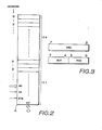
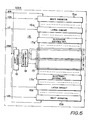
LCD 3 will now be more fully described with reference to Fig. 5. TheLCD 3 includes, as shown in Fig. 5, a liquidcrystal display panel 13 and apanel driver circuit 14 provided for driving thedisplay panel 13. The liquidcrystal display panel 13 has, for example, 640 horizontal electrodes (column electrodes) and 192 vertical electrodes (row electrodes) for displaying an image composed of a 640 x 192 dot matrix. The liquidcrystal display panel 13 is divided into two display blocks A and B of an identical construction which are independently driven. The column electrodes of the display block A are driven by a circuit comprising a 640-bit shift register 15a, a 640-bit latch circuit 16a and an electrode driving circuit 17a, while the column electrodes of the display block B are driven by another circuit comprising a 640-bit shift register 15b, a 640-bit latch circuit 16b and anelectrode driving circuit 17b. The row electrodes of the display blocks A and B are driven by a circuit comprising a 96-bit shift register 18 and anelectrode driving circuit 19. - To display an image on the liquid
crystal display panel 13 of theLCD 3, two sets of serial data for respectively displaying dots on the first (uppermost) rows of dots of the display blocks A and B are first supplied as display data LDa and LDb to theshift registers 15a and 15b, respectively, together with a shift clock SCK. When the display data LDa and LDb each composed of 640 bits have been stored respectively in theshift registers 15a and 15b, thedisplay controller 1 outputs a latch clock signal LC and a frame signal FRM• When the latch clock signals LC is outputted, the data contained in theshift registers 15a and 15b are loaded respectively onto thelatch circuits 16a and 16b, and when the frame signal FRM is outputted together with the latch clock signal LC, a bit data of "1" is stored into the first-bit stage of theshift register 18, whereby the dots on the 1st (uppermost) rows of the display blocks A and B are driven. Thedisplay controller 1 then outputs the data LDa and LDb for displaying dots on the 2nd rows of the display blocks A and B together with the shift clock signal SCK, and outputs the latch clock signal LC when the data LDa and LDb (each composed of 640 bits) are fully loaded onto theshift registers 15a and 15b. When the latch clock signal LC is outputted, the data contained in theshift registers 15a and 15b are stored into thelatch circuits 16a and 16b, and at the same time the bit data of "1" is stored into the second bit-stage of theshift register 1 8, whereby the dots on the 2nd rows of the display blocks A and B are driven. And thereafter, an operation similar to the above is repeatedly carried out to display dots on thedisplay panel 13. - Fig. 6 shows the structure of the
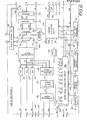
display controller 1, and Fig. 7 shows the structure of anaddress generating circuit 21 of thedisplay controller 1 of Fig. 6. Firstly, each circuit element of thedisplay controller 1 of Fig. 6 will be described. - The
display control circuit 22 effects a transfer of data between the CPU 5 (Fig. 1) and thedisplay controller 1. When theCPU 5 outputs a display unit selection data C/L (one bit), a border color code BOC (4 bits) and a start address SA, thedisplay control circuit 22 stores them respectively into aregister 23, aborder register 24 and a start address register 25 (Fig. 7). The display unit selection data C/L indicates the kind of a display unit to be selected, and is rendered "0" when a CRT display unit is used and is rendered "1" when an LCD is used. The border color code BOC designates a color of the border area or the peripheral marginal area of the screen where a display of image is not made. The start address SA indicates, as described above, that address of thevideo memory 4 where display data for the dots at the display position No. 0 of the screen is stored. When a display data is outputted from theCPU 5, thedisplay control circuit 22 supplies the display data through a buffer amplifier B1 and a terminal T6 to the data terminal DT of thevideo memory 4. At this time, thedisplay control circuit 22 enables a buffer amplifier B2 of Fig. 1, disables buffer amplifiers B3 and B4 of Fig. 6, and outputs a read/write control signal RWS (a "1" signal) to thevideo memory 4. As a result, the display data outputted from theCPU 5 is written into thevideo memory 4. The read/write control signal"RWS is normally held in a "0" state. Thedisplay control circuit 22 outputs a memory write enable signal to theCPU 5 during each non-display period such as a vertical retrace line period. - A character code CRC read out of the video memory 4 (Fig. 1) is stored into the
latch circuit 7 shown in Fig. 1, whereas color codes FCA and BCA read from thevideo memory 4 are temporarily stored into theregister 27 in response to a load signal LD1 and are then stored into theregister 28 in response to a load signal LD3.The color codes FCA and BCA thus stored in theregister 28 are supplied respectively to input terminals A and B of aselector 29. The synchronization of the signal timings can be achieved by the provision of theregister 28. - The
selector 29 outputs data fed to the input terminal A when a "1" signal is supplied to a selection terminal Sa thereof, and outputs data fed to the input terminal B when a "0" signal is supplied to the selection terminal Sa. As shown, the selection terminal Sa is supplied with the data DD outputted from the P/S converter 9-of Fig. 1. And therefore, the foreground color code FCA is outputted from theselector 29 when the data DD is "1", and the background color code BCA is outputted when the data DD is "0". - The
selector 30 outputs the color code FCA or BCA fed from theselector 29 when a "1" signal is supplied from an ANDgate 31 to a selection terminal Sa thereof. When the signal supplied to the selection terminal Sa is "0", theselector 30 outputs the border color code BOC fed from theborder register 24. The output signal of the ANDgate 31 is rendered "1" only when a display of image is effected on the screen. - The
color palette circuit 31 converts the color code outputted from theselector 30 into color data RD (red), GD (green) and BD (blue) each composed of three bits. The relationship between the color codes used and the color data RD, GD and BD is shown in Table 1.
- The DACs (Digatal-to-Analog Converters) 32 to 34 convert the color data RD, GD and BD into corresponding analog signals, respectively. Analog signals outputted from the
DACs 32 to 34 are supplied to theCRT display unit 2 of Fig. 1 as the color signals RS, GS and BS, respectively. - The
luminance calculation circuit 36 produces a luminance or an intensity data YD (3 bits) by effecting the following arithmetic operation on the color data RD, GD and BD:

- The gray-
scale display circuit 37 is provided for achieving a gray-scale display on the liquidcrystal display panel 13 of theLCD 3 in accordance with the luminance data YD. The basic principle of the gray-scale display effected in this embodiment will now be described. - In this embodiment, display of an image is performed on a frame basis, and eight consecutive frames constitute one display period. When the luminance data YD for a given dot (dot X) on the
panel 13 is "7" (black), the dot X is displayed in each of the eight frame cycles within a display period, that is to say, eight times per display period. When the luminance data YD of the dot X is "0" (white), the dot X is not displayed in any one of the eight frame cycles within a display period. On the other hand, when the luminance data YD of the dot X is any one of "1" to "6", the dot X is displayed the number of times determined by the luminance data YD within each display period. For example, when the luminance data YD is "6", the dot X is displayed seven times within one display period, and when the luminance data YD is "5", the dot is displayed six times. Thus, in this embodiment, the gray-scale display is achieved based on the number of times of display of each dot within a display period. The wording "display a dot" actually means that the dot on thepanel 1 3 is activated by a voltage, that is to say, data representative of "1" for activating the dot is loaded onto theshift register 15a or 15b shown in Fig. 5. Fig. 8 shows one example of the relationship between each luminance data YD and a display timing of the corresponding dot. It will be appreciated from Fig. 8 that when the luminance data YD for a dot to be displayed is "7", the dot is displayed in the first through eighth frame cycles within each display period. And when the luminance data YD is "4", the dot is displayed in the second, fourth, fifth, seventh and eighth frame cycles within each display period. Fig. 9 shows the construction of one example of the gray-scale display circuit 37 which outputs serial display data LD in accordance with the luminance data YD and the display timings shown in Fig. 8. As shown in Fig. 9, the gray-scale display circuit 37 comprises acounter 39 of a three-bit type which counts up the frame signal FRM. The frame signal FRM is outputted once at the beginning of each frame scanning, and therefore the output of thiscounter 39 indicates the number of the current frame cycle which is one of the frame cycles No. 0 to No. 7 shown in Fig. 8. The gray-scale display circuit 37 further comprises adecoder 40 for decoding the output of thecounter 39, adecoder 41 for decoding the luminance data YD, eight ORgates 42, eight ANDgates 43 and anOR gate 44. Each of the ORgates 42 effects a logical OR operation on signals applied to nodes (circles) of the input line thereof. And, the output signal of theOR gate 44 is supplied as the display data LD to adistribution circuit 45 of Fig. 6. - The
distribution circuit 45 outputs those bits of the display data LD used for displaying dots on the display block A as display data LDa, and outputs the remaining bits of the display data LD used for displaying dots on the display block B as display data LDb. More specifically, as the gray-scale display circuit 37 alternately outputs eight-bit serial display data for the display block A and eight-bit serial display data for the display block B, thedistribution circuit 45 latches the serial display data LD on a sixteen-bit unit basis, and serially outputs the half (eight bits) of the latched data for the display block A as the display data LDa and the other half (eight bits) for the display block B as the display data LDb in synchronization with the shift clock pulse SCK. - The
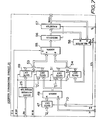
address generating circuit 21 generates address data MAD for accessing thevideo memory 4 to read data therefrom. Thisaddress generating circuit 21 comprises, as shown in Fig. 7, agate circuit 47, anadder 48, thestart address register 25, andgate circuits 49 to 52. Each of thegate circuits gate circuit 50 are supplied with "0" signals and an output of theadder 48 is supplied to the remaining upper bits of the input terminals of thegate circuit 50. And therefore, when thegate circuit 50 is opened, the output of theadder 48 is shifted four bits by thisgate circuit 50 and is outputted therefrom. Thus, when opened, thegate circuit 50 outputs data sixteen times as large as the output data of theadder 48. Similarly, the lower six bits of input terminals of thegate circuit 51 are supplied with "0" signals, and therefore, when opened, thegate circuit 51 outputs data sixty four times as large as the output data of theadder 48. Theaddress generating circuit 21 further comprises anOR circuit 53 for effecting a logical OR operation on each pair of bits of the output data of thegate circuits circuit 54 for effecting a logical OR operation on each pair of bits of the output data of thegate circuits adder 55, registers 56 and 57 each of which stores and outputs its input data at the trailing edge of a clock pulse ø1, and aselector 58. Thisaddress generating circuit 21 will be more fully described later. - The
clock pulse generator 61 shown in Fig. 6 generates a master clock pulse ø0 and the clock pulse ø1 (see Fig. 10-(b)) produced by dividing the master clock pulse 0g by eight. The flip-flop (hereinafter referred to as "FF") 62 divides the clock pulse ø1 by two to produce a clock pulse ø2 shown in Fig. 10-(c). Thehorizontal counter 63 counts up the clock pulse ø2 to form a count output indicative of the horizontal scanning position when theCRT display unit 2 is connected, the count output being indicative of the bit positions of theshift registers 15a and 15b (Fig. 5) into which data are to be stored when theLCD 3 is connected. Thevertical counter 64 counts up a signal TG outputted from the timingsignal generating circuit 65 to form a count output indicative of the vertical scanning position on the screen. The count output of thevertical counter 64 is supplied to the timingsignal generating circuit 65. Also, the upper five bits of the count output of thevertical counter 64 are supplied to input terminal B of theadder 48 shown in Fig. 7, while the lower three bits thereof are supplied as the address data LAD to thecharacter generator 8 shown in Fig. 1. - The timing
signal generating circuit 65 generates, in accordance with the clock pulses ø0 to ø2 and the count outputs of the horizontal andvertical counters signal generating circuit 65 also generates the shift clock signal SCK, the latch clock signal LC and the frame signal FRM all to be supplied to theLCD 3, and further generates other various timing signals. - Prior to beginning a display of characters, the
CPU 5 outputs the display unit selection data C/L, the border color code BOC and the data representative of the start address SA. These data are stored into theregister 23, theborder register 24 and thestart address register 25, respectively. TheCPU 5 then stores display data into thevideo memory 4. And, the display of characters on the screen is performed based on the data in theregisters 23 to 25 and thevideo memory 4 in the following manner: - When the display unit selection data C/L is "0", the
clock pulse generator 61 shown in Fig. 6 generates the master clock pulse ø0 of 14.3 MHz and the clock pulse ø1 obtained by dividing the master clock pulse ø0 by eight. The clock pulse ø1 is further divided by two by theFF 62 to form the clock pulse ø2. The waveforms of these clock pulses ø0 to ø2 are shown in Fig. 10. Thehorizontal counter 63 is triggered at each trailing edge of theclock pulse 02, so that the count output of thehorizontal counter 63 is changed as shown in Fig. 11-(b) in response to the clock signal ø2 shown in Fig. 11-(a). The timingsignal generating circuit 65 generates the signal TG shown in Fig. 11-(c) when the count output of thehorizontal counter 63 becomes "56", and supplies the generated signal TG to a reset terminal R of thehorizontal counter 63 and to a clock terminal CK of thevertical counter 64. At the trailing edge of this signal TG, thehorizontal counter 63 is reset and thevertical counter 64 is triggered. And therefore, the count output of thevertical counter 64 varies as shown in Fig. 11-(d). The numeral on the left-hand side of each hyphen shown in Fig. 11-(d) indicates the upper five bits of the count output of thevertical counter 64, and the numeral on the right-hand side of each hyphen indicates the lower three bits thereof. The signal TG shown in Fig. 11-(c) is again illustrated in Fig. 12-(a), and in response to this signal TG, the count output of thevertical counter 64 is changed as shown in Fig. 12-(b), wherein only the upper five bits of the count output are shown. When the upper five bits of the count output of thevertical counter 64 represent "32", the timingsignal generating circuit 65 outputs a reset signal VR shown in Fig. 12-(c). Thevertical counter 64 is reset at the trailing edge of the reset signal VR. - The clock pulses ø0 to ø2 and the count outputs of the horizontal and
vertical counters signal generating circuit 65 thus generates the various timing signals in accordance with the clock pulses ø0 to ø2 and the count outputs of the horizontal andvertical counters - Referring now to Fig. 7, when the display unit selection data C/L is "0", the output of the AND
gate 70 is rendered "0", so that thegate circuit 47 is closed to cause data representative of "0" to be supplied to the input terminal A of theadder 48. As a result, theadder 48 outputs the data fed to its input terminal B, that is, the upper five bits of the count output of the vertical counter 64 (the data constituted by these five bits will be hereinafter referred to as "data V"). Also, when the display unit selection data C/L is "0", theselector 58 supplies thegate circuit 52 with the data fed to the input terminal B thereof, that is, the output data of theregister 56. - The clock pulses ø1 and ø2 and the count output of the
horizontal counter 63 are again illustrated in Figs. 13-(a) to 13-(c). Shown in Figs. 13-(d) and 13-(e) are waveforms of signals M64 and M16 outputted from the timingsignal generating circuit 65. When the signal M64 of "1" is outputted from the timingsignal generating circuit 65, thegate circuits gate circuit 50 is opened. On the other hand, thegate circuit 52 is opened when the signal M64 is rendered "0". Shown in Fig. 13-(f) is the waveform of a signal CiS which is supplied to a carry input terminal Ci of theadder 55 of Fig. 7. - When the signal M64 is rendered "1" at time to shown in Fig. 13, the
gate circuit 49 is opened, so that the data representing the start address SA and contained in thestart address register 25 is supplied through thegate circuit 49 to one input terminals of theOR circuit 53. At this time, thegate circuit 50 is closed, so that the other input terminals of theOR circuit 53 are supplied with data representative of "0". As a result, theOR circuit 53 outputs the data representing the start address SA to the input terminal A of the adder 55 (see Fig. 13-(g)). Also, when the signal M64 is rendered "1" at the time to, thegate circuit 51 is opened, so that it outputs data sixty four times as large as the data V (i. e., 64V) to one input terminals of theOR circuit 54. At this time, thegate circuit 52 is closed, so that thedata 64V is supplied to the input terminal B of the adder 55 (see Fig. 13-(h)). Consequently, the data outputted from theadder 55 at the time to becomes equal to "SA + 64V" (Fig. 13-(i)). - At time t1, the data "SA + 64V" outputted from the
adder 55 is stored into theregister 56 and thence supplied through theselector 58 to the input terminal of thegate circuit 52. At this time, the signal M64 falls and the signal M16 rises. As a result, at this time t1 data "16V" outputted from thegate circuit 50 is supplied through theOR circuit 53 to the input terminal A of the adder 55 (see Fig. 13-(g)), while the data "SA + 64V" outputted from thegate circuit 52, that is, the output of theregister 56, is supplied through theOR circuit 54 to the input terminal B of the adder 55 (Fig. 13 (h)). Consequently, data "SA + 80V" is outputted from the adder 55 (Fig. 13-(i)). At time t2, the data "SA + 80V" outputted from theadder 50 and the data "SA + 64V" outputted from theregister 56 are stored respectively into theregisters gate circuits 49 to 51 and to open thegate circuit 52. As a result, data representative of "0" and the data "SA + 80V" outputted from theregister 56 are supplied to the input terminals A and B of theadder 55, so that theadder 55 continues to output the data "SA + 80V". At time t3, data at the input and output terminals of theadder 55 and the output data of theregisters video memory 4 shown in Fig. 1. Each arrow in Fig. 13 indicates that the data is the same as the next data on the left side. - At time t4, data "SA + 80V" are stored respectively into the
registers adder 55. At this time t4, the signal CiS is rendered "1", and therefore, theadder 55 outputs data representative of "SA + 80V + 1". At the next time t5, the output data of theadder 55, register 56 and register 57 become equal to "SA + 80V + 2", "SA + 80V + 1" and "SA + 80V", respectively (see Figs. 13-(i), 13-(j) and 13-(k)). And, at time t6, the output data of theadder 55, register 56 and register 57 become equal to "SA + 80V + 3", "SA + 80V + 2" and "SA + 80V + 1", respectively. And thereafter, an operation similar to the above is repeatedly carried out. - Once the signal CiS is rendered "0" at time t7 which comes in the middle of the period when the count output of the
horizontal counter 63 is "41", the output data of theadder 55 which now represents "SA + 80V + 80" is thereafter kept unchanged, and the outputs of theregisters horizontal counter 63 again becomes equal to "55", the signal M64 is again outputted, whereby an operation similar to the above is repeated. - As will be appreciated from Fig. 13-(k), during the time when the count output of the
horizontal counter 63 varies from "2" to "41", the address data MAD'is changed from "SA + 80V" to "SA + 80V + 79". For example, if both of the data SA and V are "0", the address data MAD is changed from "0" to "79" as shown in Fig. 13-(m), and if the data SA is "0" but the data V is "1", the address data MAD is changed from "80" to "159" as shown in Fig. 13-(n). It should be noted that the address data MAD thus produced is effective only when the count output of thehorizontal counter 63 is within the range of from "2" to "41". When the count output of thehorizontal counter 63 is not within the above range, data read from thevideo memory 4 by the address data MAD are not used for the actual display operation. - As will be seen from Figs. 12-(a) and 12-(b), when the upper five bits of the count output of the vertical counter 64 (that is, the data V) is "0", the signal TG is outputted eight times. On the other hand, the cycle of the signal TG is equal to that of the count operation of the
horizontal counter 63. And therefore, if the start address SA is "0", the address data MAD is changed from "0" to "79" eight times while the data V is "0". And, data are read from thevideo memory 4 by these address data MAD to effect a display of characters on the first row (the uppermost row) shown in Fig. 4 as will be more fully described later. When the data V is "1", the address data MAD is changed from "80" to "159" eight times to read from thevideo memory 4 data for displaying characters on the second row, and, when the data V is "23" a display of characters is effected on the lowermost row. On the other hand, a non-display period including the vertical retrace time is provided when the data V is within the range of from "24" to "32". The reason why the same address data MAD is outputted eight times is that each character is constituted by eight rows of dots. - Figs. 14-(a) to 14-(c) show the clock pulse ø1, the count output of the
horizontal counter 63 and the address data MAD, wherein it is assumed that the start address SA is "0". It is also assumed that within the time range of Fig. 1 4 the count output of thevertical counter 64 is "0 - 0", that is to say, both of the upper five bits and lower three bits of the count output of thevertical counter 64 are "0". And therefore, time t10 shown in Fig. 1 4 is equal to the time t10 shown in Fig. 11. Shown in Fig. 14-(d) is the waveform of the signal ESS outputted from the timingsignal generating circuit 65 to the terminal CS of thevideo memory 4 shown in Fig. 1, Fig. 14-(e) the waveform of the load signal LDO supplied to the load terminal L of the latch circuit 7 (Fig. 1), Fig. 14-(f) the waveform of the load signal LD1 supplied to the load terminal L of the register 27 (Fig. 6), Fig. 14-(g) the waveform of the load signal LD2 supplied to the load terminal L of the P/S converter ) (Fig. 1), Fig. 14-(h) the waveform of the load signal LD3 supplied to the load terminal L of the register 28 (Fig. 6), and Fig. 14-(i) the waveform of the clock pulse ø0 (Fig. 10-(a)) supplied to the clock terminal CK of the P/S converter 9. - When the address data MAD and the signal ESS in the "0" state are outputted to the
memory 4 at the time t10 shown in Fig. 14, the character code CRC is read from the address "0" in the area Eo of thememory 4, this character code being hereinafter referred to as "CRC-0". When the load signal LDO is outputted to thelatch circuit 7 at the next time t11, the character code CRC-0 is stored into thelatch circuit 7 and thence outputted to the address terminal AD1 of thecharacter generator 8. At this time, the address terminal AD0 of thecharacter generator 8 is supplied with the address data LAD (the lower three bits of the count output of the vertical counter 64) representative of "0". And therefore, when the character code CRC-0 is supplied to thecharacter generator 8, an eight-bit dot pattern of the first row of the character pattern designated by the character code CRC-0 is read from thecharacter generator 8 and supplied to the P/S converter 9. At time t12, the signal ESS is rendered "1", so that the color codes FCA and BCA are read from the address "0" of the area E1 of thevideo memory 4. When the load signal LD1 is outputted to theregister 27 shown in Fig. 6 at time t13, the color codes FCA and BCA read from thememory 4 are stored into theregister 27. At the next time t14, the load signal LD2 is supplied to the P/S converter 9, so that the dot pattern read from thecharacter generator 8 is stored into the P/S converter 9. And, when the load signal LD3 is supplied to the load terminal L of theregister 28 at time t15, the color codes FCA and BCA in theregister 27 are stored into theregister 28. The dot pattern stored in the P/S converter 9 is then serially outputted as the data DD in accordance with the clock pulse ø0 and supplied to the selection terminal Sa of the selector 29 (Fig. 6) as shown in Fig. 14-(j). Thus, when the data DD is "1" theselector 29 outputs the foreground color code FCA to theselector 30, and when the data DD is "0" theselector 29 outputs the background color code BCA to theselector 30. At this time, the selection terminal Sa of theselector 30 is supplied with a "1" signal as will be described later. And therefore, the color code FCA or BCA thus outputted from theselector 29 is supplied through theselector 30 to thecolor palette circuit 31 to be converted into the color data RD, GD and BD. The color data RD, GD and BD thus obtained are then converted respectively into the analog color signals RS, GS and BS by theDACs 32 to 34 and supplied to theCRT display unit 2. On the other hand, the timingsignal generating circuit 65 supplies theCRT display unit 2 with the horizontal synchronization signal HSY shown in Fig. 11-(e) and the vertical synchronization signal VSY shown in Fig. 12-(d). And therefore, when the color signals RS, GS and BS are supplied to theCRT display unit 2, the eight dots on the first row of the dot-matrix at the display position No. 0 shown in Fig. 4 are displayed in colors determined by the color signals RS, GS and BS. Thus, when the P/S converter 9 (Fig. 1) outputs the data DD of eight bits during the time period between the time t15 and the time t1 6, a color display of dots is made on the first row of the dot-matrix at the display position No. 0. - On the other hand, during the time period between the time t15 and the time t1 6, the address data MAD is rendered "1" and in addition the signals ESS and LDO to LD3 are outputted in accordance with the same timings as those signals outputted during the time period between the time t10 and the time t15. As a result, the first row portion (dot pattern) of the character pattern designated by the character code CRC-1 in the address "1" of the area EO of the
memory 4 is loaded onto the P/S converter 9 at the time t16. Also, the color codes FCA and BCA in the address "1" of the area E1 of thememory 4 are stored into theregister 28. And, when the dot pattern in the P/S converter 9 is serially outputted as the data DD during the period between the time t16 and the time t17, display of dots is made on the first row of the dot-matrix at the display position No. 1. And thereafter, a display operation similar to the above is repeatedly carried out. Fig. 11-(f) shows the address data MAD varying in accordance with the above operation, and Fig. 11-(g) shows the positions of the dots and their display timings. - When all of the dots on-the first rows of the dot-matrices of the display position Nos. 0 to 79 have been displayed, the count output of the
vertical counter 64 is changed to "0 - 1" (see Fig. 11-(d) at time t20), so that data representative of "1" is supplied as the address data LAD to the address terminal ADO of thecharacter generator 8. And, during the time when the count output of thehorizontal counter 63 varies from "2" to "41", the dots on the second rows of the dot-matrices of the display position Nos. 0 to 79 are displayed (see Fig. 11-(g)). Thus, when the upper five bits of the count output of thevertical counter 64 is "0", the dots on the first to eighth rows of the dot-matrices of the display position Nos. 0 to 79 are sequentially displayed. In the similar manner, when the upper five bits of the count output of thevertical counter 64 is "1", display of the dots of the dot-matrices of the display position Nos. 80 to 159 is made, ... and when the upper five bits of the count output of thevertical counter 64 is "23", display of the dots of the dot-matrices of the display position Nos. 1840 to 1919 is made. - The waveforms of the signals HD and VD both generated by the timing
signal generating circuit 65 are shown in Fig. 11-(h) and in Fig. 12-(e), respectively. As will be appreciated from Figs. 11 and 12, these signals HD and VD should be rendered "1'' when theselector 29 shown in Fig. 6 outputs color codes to display dots on the screen. And therefore, the output of the ANDgate 31 fed to the selection terminal Sa of the selector 30 (Fig. 6) is rendered "1" during the time when the display of dots are actually performed, and is rendered "0" during other periods. Thus, during the non-display periods, theselector 30 outputs the border color code BOC contained in theborder register 24. And, the border area surrounding the 640 X 192 display positions is displayed in accordance with this border color code BOC. - The waveforms of the clock pulses ø0 to ø2 in this case are the same as those shown in Fig. 10, but the period of the clock pulse ø0 is now 10.7 MHz. The waveforms of the clock pulse ø2 in this case is shown in Fig. 15-(a), the variation of the count output of the
horizontal counter 63 in Fig. 15-(b), the waveform of the signal TG in Fig. 15-(c), and the variation of the count output of thevertical counter 64 in Fig. 15-(d). Shown in Figs. 15-(e) and 15-(f) are the waveforms of the latch clock signal LC and the frame signal FRM, respectively. As shown, the latch clock signal LC is outputted each time the count output of thehorizontal counter 63 becomes equal to "85", while the frame signal FRM is outputted when the count output of thehorizontal counter 63 is equal to "85" and when the count output of thevertical counter 64 is equal to "0 - 0". Thus, the frame signal FRM is outputted once per vertical scanning. The latch clock LC and the frame signal FRM thus outputted are supplied to theLCD 3. Figs. 15-(g) and 15-(h) show the waveforms of the signals HD and HD1 outputted from the timingsignal generating circuit 65, the signal HD1 being supplied to one input terminal of the AND gate 68 (Fig. 6). A flip-flop 69 divides the clock pulse ø0 by two to produce a clock pulse ø0a which is supplied to the other input terminal of the ANDgate 68. When the signal HD1 is in the "1" state, this clock pulse ø0a passes through the ANDgate 68 and is thence supplied as the shift clock signal SCK to theLCD 3 and the distribution circuit 45 (see Fig. 19). Fig. 16-(a) shows the signal TC, Fig. 16-(b) the variation of the upper five bits of the count output of thevertical counter 64, Fig. 16-(c) the reset signal VR to thevertical counter 64, and Fig. 16-(d) the signal VD. - When the
LCD 3 is connected, data representative of "1" is stored in the register 23 (Fig. 6) as the display unit selection data C/L. When the display unit selection data C/L is rendered "1", the ANDgate 70 shown in Fig. 7 is enabled to open, so that the clock pulse ø2 is supplied to thegate circuit 47. As a result, when the clock pulse ø2 is in the "0" state, data representative of "0" is supplied to the input terminal A of theadder 48, whereas data representative of "12" is supplied to the input terminal A when the clock pulse ø2 is in the "1" state. The data representative of "12" corresponds to the number of rows of the character display positions in the display block A (see Figs. 4 and 5). When the display unit selection data C/L is "1", the output data of theregister 57 is supplied through theselector 58 to thegate circuit 52. - Fig. 17 corresponds to Fig. 13 and shows the timings of the signals generated when the
LCD 3 is connected. The signals M64,M1 6 and CiS generated when theLCD 3 is connected are different in timing from those generated when theCRT 2 is connected. Also, the data supplied respectively to the input terminal A of theadder 48 and the input terminal of thegate circuit 52 when theCRT 2 is connected are different from those supplied when theLCD 3 is connected. However, each circuit element shown in Fig. 7 performs the same operation in both cases. And, in the case where theLCD 3 is connected, the address data MAD varies as shown in Fig. 17-(k). More specifically, if both of the start address SA and the data V (the upper five bits of the count output of the vertical counter 64) are "0", as shown in Fig. 17-(m), data representative of "0" and "80 X 12" (or "960") are sequentially outputted when the count output of thehorizontal counter 63 is "4", data representative of "1" and "80X 1 + 1" (or "961") are sequentially outputted when the count output is "5", ... and data representative of "79" and "80 X 12 + 79" (or "1039") when the count output is "83". The data representative of "0", "1", "2", ... "79" designate those addresses of thevideo memory 4 in which the character codes CRC of the characters to be displayed on the first row of display positions in the display block A are stored. On the other hand, the data representative of "960", "961", ... "1039" designate those addresses of thevideo memory 4 in which the character codes CRC of the characters to be displayed on the first row of display positions in the display block B are stored. Similarly, when the start address SA is "0" but the data V is "1", as shown in Fig. 17-(n), data indicative of the addresses storing the character codes CRC of the characters to be displayed on the second rows of display positions in the display blocks A and B are alternately outputted during the time when the count output of thehorizontal counter 63 varies from "4" to "83". The similar operation is performed when the data V takes any one of "2" to "11". - Thus, as shown in Fig. 17, data indicative of the addresses storing character codes of the characters to be displayed in the display blocks A and B are outputted in a time sharing manner.
- Fig. 18 is a timing chart corresponding to that shown in Fig. 14, wherein it is assumed that the count output of the
vertical counter 64 is "0 - 0". During the period between the time t30 and the time t31 in Fig. 18, the character code CRC-0 and the color codes FCA and BCA are read respectively from the address "0" of the area Eo and the address "0" of the area E1 of thevideo memory 4. The read color codes FCA and BCA are stored into theregister 28 shown in Fig. 6, and the dot pattern of the first row of dots of the character pattern designated by the read character code CRC-0 is stored into the P/S converter 9. During the period between the time t31 and the time t32, the dot pattern in the P/S converter 9 is serially supplied as data DD to theselector 29, so that the color codes FCA and BCA in theregister 28 are selectively outputted therefrom. Each of the thus outputted color codes is converted into color data RD, GD and BD by thecolor palette circuit 31. Theluminance calculation circuit 36 converts the color data RD, GD and BD into luminance data YD which is then converted into display data LD to be supplied to thedistribution circuit 45. - On the other hand, during the period between the time t31 and the time t32, the character code CRC and the color codes FCA and BCA are read respectively from the addresses "960" of the areas Eo and E1 of the
video memory 4. And, these read character and color codes are loaded onto the P/S converter 9 and theregister 28. Then, during the period between the time t32 and the time t33, the data in the P/S converter 9 is serially outputted as the data DD to theselector 29. Consequently, the color codes FCA and BCA are selectively outputted from theselector 29 and converted into the display data LD which is then fed to thedistribution circuit 45. And thereafter, an. operation similar to the above is repeated. - The
distribution circuit 45 latches the data LD (Fig. 19-(b)) on a sixteen-bit unit basis and outputs those bits of the latched data LD for the display block A as data LDa in accordance with the shift clock SCK, as shown in Fig. 19-(e). Thedistribution circuit 45 also outputs those bits of the latched data LD for the display block B as data LDb in accordance with the shift clock SCK, as shown in Fig. 19-(f). The thus outputted data LDa and LDb are shifted into theshift registers 15a and 15b, and then loaded into thelatch circuits 16a and 16b by the latch clock LC, whereby display of dots is made in accordance with the loaded data LDa and LDb. - The above-described display system is so designed as to display characters, however it is apparent that the present invention can be applied to a graphic display system of a dot- map type.
Claims (6)
Applications Claiming Priority (2)
| Application Number | Priority Date | Filing Date | Title |
|---|---|---|---|
| JP60055127A JPS61213896A (en) | 1985-03-19 | 1985-03-19 | Display controller |
| JP55127/85 | 1985-03-19 |
Publications (3)
| Publication Number | Publication Date |
|---|---|
| EP0195203A2 true EP0195203A2 (en) | 1986-09-24 |
| EP0195203A3 EP0195203A3 (en) | 1990-06-13 |
| EP0195203B1 EP0195203B1 (en) | 1993-09-29 |
Family
ID=12990094
Family Applications (1)
| Application Number | Title | Priority Date | Filing Date |
|---|---|---|---|
| EP86101119A Expired - Lifetime EP0195203B1 (en) | 1985-03-19 | 1986-01-28 | Display controller |
Country Status (4)
| Country | Link |
|---|---|
| US (1) | US4760387A (en) |
| EP (1) | EP0195203B1 (en) |
| JP (1) | JPS61213896A (en) |
| DE (1) | DE3689077T2 (en) |
Cited By (24)
| Publication number | Priority date | Publication date | Assignee | Title |
|---|---|---|---|---|
| EP0244978A2 (en) * | 1986-04-25 | 1987-11-11 | Seiko Instruments Inc. | Interface, for example for a liquid crystal display device |
| EP0295690A2 (en) * | 1987-06-19 | 1988-12-21 | Kabushiki Kaisha Toshiba | Display area control system for plasma display apparatus |
| EP0295689A2 (en) * | 1987-06-19 | 1988-12-21 | Kabushiki Kaisha Toshiba | Display controller for CRT/plasma display apparatus |
| EP0295691A2 (en) | 1987-06-19 | 1988-12-21 | Kabushiki Kaisha Toshiba | Display mode switching system for plasma display apparatus |
| EP0340664A2 (en) * | 1988-04-30 | 1989-11-08 | Kabushiki Kaisha Toshiba | Method and system for setting palette data by a display mode |
| EP0344621A2 (en) * | 1988-05-28 | 1989-12-06 | Kabushiki Kaisha Toshiba | Plasma display control system |
| EP0354480A2 (en) * | 1988-08-09 | 1990-02-14 | Seiko Epson Corporation | Display signal generator |
| EP0359236A2 (en) * | 1988-09-13 | 1990-03-21 | Kabushiki Kaisha Toshiba | Display control apparatus for converting color/monochromatic CRT gradation into PDP gradation |
| EP0359234A2 (en) * | 1988-09-13 | 1990-03-21 | Kabushiki Kaisha Toshiba | Display control apparatus for converting CRT resolution into PDP resolution by hardware |
| EP0360402A2 (en) * | 1988-09-22 | 1990-03-28 | International Business Machines Corporation | Digital data display system |
| EP0384442A2 (en) * | 1989-02-22 | 1990-08-29 | Sharp Kabushiki Kaisha | Display control apparatus for reproducing color image on crt display device and matrix type display device |
| EP0403268A2 (en) * | 1989-06-15 | 1990-12-19 | Matsushita Electric Industrial Co., Ltd. | Video signal compensation apparatus |
| EP0421772A2 (en) * | 1989-10-06 | 1991-04-10 | Canon Kabushiki Kaisha | Display apparatus |
| FR2657987A1 (en) * | 1990-02-06 | 1991-08-09 | Commissariat Energie Atomique | METHOD FOR CONTROLLING A MATRIX SCREEN COMPRISING TWO INDEPENDENT PARTS AND DEVICE FOR ITS IMPLEMENTATION. |
| EP0530762A2 (en) * | 1991-09-06 | 1993-03-10 | Texas Instruments Incorporated | DMD display system controller |
| US5218274A (en) * | 1989-07-31 | 1993-06-08 | Kabushiki Kaisha Toshiba | Flat panel display controller using dual-port memory |
| US5293485A (en) * | 1988-09-13 | 1994-03-08 | Kabushiki Kaisha Toshiba | Display control apparatus for converting color/monochromatic CRT gradation into flat panel display gradation |
| US5448260A (en) * | 1990-05-07 | 1995-09-05 | Kabushiki Kaisha Toshiba | Color LCD display control system |
| US5491496A (en) * | 1991-07-31 | 1996-02-13 | Kabushiki Kaisha Toshiba | Display control device for use with flat-panel display and color CRT display |
| US5548765A (en) * | 1990-08-28 | 1996-08-20 | Seiko Epson Corporation | Power saving display subsystem for portable computers |
| WO1997034220A1 (en) * | 1996-03-12 | 1997-09-18 | Siemens Nixdorf Informationssysteme Ag | Operation of several visual devices on one visual display system |
| WO1999044189A1 (en) * | 1998-02-26 | 1999-09-02 | Coms21 Limited | A method of driving and backlighting an lcd of card reader |
| US6124842A (en) * | 1989-10-06 | 2000-09-26 | Canon Kabushiki Kaisha | Display apparatus |
| US6844864B2 (en) | 2001-02-24 | 2005-01-18 | Diehl Ako Stiftung & Co., Kg | Circuit arrangement for actuating a display |
Families Citing this family (62)
| Publication number | Priority date | Publication date | Assignee | Title |
|---|---|---|---|---|
| JPS622298A (en) * | 1985-06-28 | 1987-01-08 | 富士通株式会社 | Display control system for liquid crystal display crt controller |
| JPS6219897A (en) * | 1985-07-19 | 1987-01-28 | 富士通株式会社 | Liquid crystal display control system by crt controller |
| DE3632601A1 (en) * | 1985-09-27 | 1987-04-23 | Olympus Optical Co | DEVICE FOR DISPLAYING A POSITION BRAND ON SEVERAL SCREENS |
| US4825390A (en) * | 1986-04-28 | 1989-04-25 | Texas Instruments, Inc. | Color palette having repeat color data |
| EP0295692B1 (en) * | 1987-06-19 | 1994-11-23 | Kabushiki Kaisha Toshiba | crt/plasma display controller |
| JP2892000B2 (en) * | 1987-06-19 | 1999-05-17 | 株式会社東芝 | Display control method |
| US5351064A (en) * | 1987-06-19 | 1994-09-27 | Kabushiki Kaisha Toshiba | CRT/flat panel display control system |
| KR930001681B1 (en) * | 1987-08-31 | 1993-03-08 | 세이꼬 엡슨 가부시끼가이샤 | Video signal processor |
| JPH01248185A (en) * | 1988-03-30 | 1989-10-03 | Toshiba Corp | Display controller |
| JPH01248186A (en) * | 1988-03-30 | 1989-10-03 | Toshiba Corp | Display attribute converting device |
| US5592194A (en) * | 1988-04-27 | 1997-01-07 | Seiko Epson Corporation | Display controller |
| JP2892009B2 (en) * | 1988-05-28 | 1999-05-17 | 株式会社東芝 | Display control method |
| US5225875A (en) * | 1988-07-21 | 1993-07-06 | Proxima Corporation | High speed color display system and method of using same |
| US5276436A (en) * | 1988-07-21 | 1994-01-04 | Proxima Corporation | Television signal projection system and method of using same |
| US5264835A (en) * | 1988-07-21 | 1993-11-23 | Proxima Corporation | Enhanced color display system and method of using same |
| US5300944A (en) * | 1988-07-21 | 1994-04-05 | Proxima Corporation | Video display system and method of using same |
| JP2773248B2 (en) * | 1988-08-09 | 1998-07-09 | セイコーエプソン株式会社 | Image signal processing device |
| JPH0269799A (en) * | 1988-09-06 | 1990-03-08 | Toshiba Corp | Display controller |
| US5285192A (en) * | 1988-09-16 | 1994-02-08 | Chips And Technologies, Inc. | Compensation method and circuitry for flat panel display |
| US5222212A (en) * | 1988-09-16 | 1993-06-22 | Chips And Technologies, Inc. | Fakeout method and circuitry for displays |
| WO1990003011A1 (en) * | 1988-09-16 | 1990-03-22 | Chips And Technologies, Inc. | Fakeout method and circuitry for displays |
| KR900702500A (en) * | 1988-09-16 | 1990-12-07 | 원본미기재 | Flat panel display compensation method and circuit |
| US5261046A (en) * | 1988-12-27 | 1993-11-09 | Eastman Kodak Company | Resequencing line store device |
| US5150109A (en) * | 1989-02-13 | 1992-09-22 | Touchstone Computers, Inc. | VGA controller card |
| US5185602A (en) * | 1989-04-10 | 1993-02-09 | Cirrus Logic, Inc. | Method and apparatus for producing perception of high quality grayscale shading on digitally commanded displays |
| KR910006834A (en) * | 1989-09-29 | 1991-04-30 | 아오이 죠이치 | Display control device which can change the brightness by the condition of power circuit |
| JPH03126073A (en) * | 1989-10-11 | 1991-05-29 | Nakajima All Precision Kk | Lcd display |
| US5227772A (en) * | 1990-01-30 | 1993-07-13 | Mitsubishi Denki Kabushiki Kaisha | Text display apparatus and a method of displaying text |
| JPH03225393A (en) * | 1990-01-30 | 1991-10-04 | Mitsubishi Electric Corp | Text display device |
| JP3137367B2 (en) * | 1990-08-09 | 2001-02-19 | 株式会社東芝 | Color panel display control system and computer system |
| JPH06501322A (en) * | 1990-09-21 | 1994-02-10 | プロクシマ コーポレイション | High-speed color display projection system and its usage |
| JPH0743581B2 (en) * | 1990-10-31 | 1995-05-15 | ヤマハ株式会社 | Display controller |
| US5309168A (en) * | 1990-10-31 | 1994-05-03 | Yamaha Corporation | Panel display control device |
| JP2578251B2 (en) * | 1990-11-09 | 1997-02-05 | シャープ株式会社 | Image display device |
| EP0520454B1 (en) * | 1991-06-26 | 1998-10-14 | Kabushiki Kaisha Toshiba | Display control system for determining connection of optional display unit by using palette |
| JPH0588846A (en) * | 1991-09-30 | 1993-04-09 | Toshiba Corp | Flat panel display control system |
| US5422654A (en) | 1991-10-17 | 1995-06-06 | Chips And Technologies, Inc. | Data stream converter with increased grey levels |
| US5751265A (en) * | 1991-12-24 | 1998-05-12 | Cirrus Logic, Inc. | Apparatus and method for producing shaded images on display screens |
| WO1993013513A1 (en) * | 1991-12-24 | 1993-07-08 | Cirrus Logic, Inc. | Process for producing shaded images on display screens |
| US5841430A (en) * | 1992-01-30 | 1998-11-24 | Icl Personal Systems Oy | Digital video display having analog interface with clock and video signals synchronized to reduce image flicker |
| JPH0651727A (en) * | 1992-06-04 | 1994-02-25 | Toshiba Corp | Display control method and controller therefor |
| JP3096362B2 (en) * | 1992-10-26 | 2000-10-10 | 沖電気工業株式会社 | Serial access memory |
| DE69421832D1 (en) * | 1993-01-11 | 2000-01-05 | Canon Kk | Color display device |
| GB2282906B (en) | 1993-10-13 | 1996-11-06 | Dataquill Ltd | Data enty systems |
| JPH0836371A (en) * | 1994-07-22 | 1996-02-06 | Toshiba Corp | Display controller |
| US5877741A (en) * | 1995-06-07 | 1999-03-02 | Seiko Epson Corporation | System and method for implementing an overlay pathway |
| US5694141A (en) * | 1995-06-07 | 1997-12-02 | Seiko Epson Corporation | Computer system with double simultaneous displays showing differing display images |
| US5892496A (en) * | 1995-12-21 | 1999-04-06 | Advanced Micro Devices, Inc. | Method and apparatus for displaying grayscale data on a monochrome graphic display |
| US5977933A (en) * | 1996-01-11 | 1999-11-02 | S3, Incorporated | Dual image computer display controller |
| US6020863A (en) * | 1996-02-27 | 2000-02-01 | Cirrus Logic, Inc. | Multi-media processing system with wireless communication to a remote display and method using same |
| US5903283A (en) * | 1997-08-27 | 1999-05-11 | Chips & Technologies, Inc. | Video memory controller with dynamic bus arbitration |
| KR100251499B1 (en) * | 1997-11-25 | 2000-04-15 | 윤종용 | The method of hot-plugging |
| US6823016B1 (en) * | 1998-02-20 | 2004-11-23 | Intel Corporation | Method and system for data management in a video decoder |
| EP1026654B1 (en) * | 1999-01-29 | 2007-03-21 | Canon Kabushiki Kaisha | Flat picture display apparatus with image position adjustment |
| JP4056672B2 (en) * | 2000-02-29 | 2008-03-05 | シャープ株式会社 | Semiconductor device and display device module |
| US7009616B2 (en) * | 2000-05-22 | 2006-03-07 | Silicon Graphics, Inc. | Multi-mode display |
| US7138989B2 (en) * | 2000-09-15 | 2006-11-21 | Silicon Graphics, Inc. | Display capable of displaying images in response to signals of a plurality of signal formats |
| US6842160B2 (en) * | 2000-11-21 | 2005-01-11 | Canon Kabushiki Kaisha | Display apparatus and display method for minimizing decreases in luminance |
| JP2003066938A (en) * | 2001-08-24 | 2003-03-05 | Sharp Corp | Display controller, display control method and image display system |
| DE10208073B4 (en) * | 2002-02-25 | 2006-06-08 | Diehl Ako Stiftung & Co. Kg | Driver circuit for an LCD display |
| TWI247244B (en) * | 2004-05-28 | 2006-01-11 | Via Tech Inc | Image processing device |
| TWI471823B (en) * | 2008-07-31 | 2015-02-01 | Pixart Imaging Inc | Method of determining coordinate on micro dotmap according to moving vector |
Citations (1)
| Publication number | Priority date | Publication date | Assignee | Title |
|---|---|---|---|---|
| EP0066983A2 (en) | 1981-05-27 | 1982-12-15 | SORD Computer Systems, Inc. | Method of and apparatus for controlling the display of video signal information |
Family Cites Families (14)
| Publication number | Priority date | Publication date | Assignee | Title |
|---|---|---|---|---|
| US3559208A (en) * | 1966-05-06 | 1971-01-26 | Bunker Ramo | Data display means |
| US4149152A (en) * | 1977-12-27 | 1979-04-10 | Rca Corporation | Color display having selectable off-on and background color control |
| US4201983A (en) * | 1978-03-02 | 1980-05-06 | Motorola, Inc. | Addressing circuitry for a vertical scan dot matrix display apparatus |
| GB2056228B (en) * | 1979-07-04 | 1983-04-20 | New Nippon Electric Co | Cathode-ray tube display device |
| DE3039843A1 (en) * | 1979-10-22 | 1981-04-30 | Casio Computer Co., Ltd., Tokyo | TIME DISPLAY DEVICE |
| JPS57114190A (en) * | 1981-01-07 | 1982-07-15 | Hitachi Ltd | Matrix display device |
| FR2506623A1 (en) * | 1981-06-01 | 1982-12-03 | Radiotechnique | THREE-COLOR VIDEO SIGNAL GENERATOR, SUCH AS A VIDEO GAME, FOR USE WITH A MONOCHROME IMAGE REPRODUCER |
| JPS5859490A (en) * | 1981-10-06 | 1983-04-08 | 株式会社東芝 | Display controller |
| US4536856A (en) * | 1982-06-07 | 1985-08-20 | Sord Computer Systems, Inc. | Method of and apparatus for controlling the display of video signal information |
| JPS5991487A (en) * | 1982-11-17 | 1984-05-26 | 富士通株式会社 | Display unit |
| JPS59176985A (en) * | 1983-03-26 | 1984-10-06 | Citizen Watch Co Ltd | Liquid crystal television receiver |
| JPS59176834A (en) * | 1983-03-28 | 1984-10-06 | Canon Inc | Portable terminal device |
| US4591842A (en) * | 1983-05-26 | 1986-05-27 | Honeywell Inc. | Apparatus for controlling the background and foreground colors displayed by raster graphic system |
| JPS60227296A (en) * | 1984-04-25 | 1985-11-12 | シャープ株式会社 | Display control system |
-
1985
- 1985-03-19 JP JP60055127A patent/JPS61213896A/en active Granted
-
1986
- 1986-01-28 EP EP86101119A patent/EP0195203B1/en not_active Expired - Lifetime
- 1986-01-28 DE DE86101119T patent/DE3689077T2/en not_active Expired - Lifetime
- 1986-01-31 US US06/824,953 patent/US4760387A/en not_active Expired - Lifetime
Patent Citations (1)
| Publication number | Priority date | Publication date | Assignee | Title |
|---|---|---|---|---|
| EP0066983A2 (en) | 1981-05-27 | 1982-12-15 | SORD Computer Systems, Inc. | Method of and apparatus for controlling the display of video signal information |
Cited By (44)
| Publication number | Priority date | Publication date | Assignee | Title |
|---|---|---|---|---|
| EP0244978A2 (en) * | 1986-04-25 | 1987-11-11 | Seiko Instruments Inc. | Interface, for example for a liquid crystal display device |
| EP0244978A3 (en) * | 1986-04-25 | 1989-01-04 | Seiko Instruments Inc. | Interface, for example for a liquid crystal display device |
| EP0295690A2 (en) * | 1987-06-19 | 1988-12-21 | Kabushiki Kaisha Toshiba | Display area control system for plasma display apparatus |
| EP0295689A2 (en) * | 1987-06-19 | 1988-12-21 | Kabushiki Kaisha Toshiba | Display controller for CRT/plasma display apparatus |
| EP0295691A2 (en) | 1987-06-19 | 1988-12-21 | Kabushiki Kaisha Toshiba | Display mode switching system for plasma display apparatus |
| EP0295690A3 (en) * | 1987-06-19 | 1991-03-27 | Kabushiki Kaisha Toshiba | Display area control system for plasma display apparatus |
| EP0295689A3 (en) * | 1987-06-19 | 1991-03-27 | Kabushiki Kaisha Toshiba | Display controller for crt/plasma display apparatus |
| EP0295691A3 (en) * | 1987-06-19 | 1991-03-13 | Kabushiki Kaisha Toshiba | Display mode switching system for plasma display apparatus |
| EP0340664A2 (en) * | 1988-04-30 | 1989-11-08 | Kabushiki Kaisha Toshiba | Method and system for setting palette data by a display mode |
| EP0340664A3 (en) * | 1988-04-30 | 1991-06-12 | Kabushiki Kaisha Toshiba | Method and system for setting palette data by a display mode |
| EP0344621A2 (en) * | 1988-05-28 | 1989-12-06 | Kabushiki Kaisha Toshiba | Plasma display control system |
| EP0344621A3 (en) * | 1988-05-28 | 1991-07-31 | Kabushiki Kaisha Toshiba | Plasma display control system |
| EP0354480A3 (en) * | 1988-08-09 | 1991-10-23 | Seiko Epson Corporation | Display signal generator |
| EP0354480A2 (en) * | 1988-08-09 | 1990-02-14 | Seiko Epson Corporation | Display signal generator |
| US5508714A (en) * | 1988-09-13 | 1996-04-16 | Kabushiki Kaisha Toshiba | Display control apparatus for converting CRT resolution into PDP resolution by hardware |
| US5438652A (en) * | 1988-09-13 | 1995-08-01 | Kabushiki Kaisha Toshiba | Display control apparatus for converting color/monochromatic CRT gradation into flat panel gradation |
| US5293485A (en) * | 1988-09-13 | 1994-03-08 | Kabushiki Kaisha Toshiba | Display control apparatus for converting color/monochromatic CRT gradation into flat panel display gradation |
| EP0359234A2 (en) * | 1988-09-13 | 1990-03-21 | Kabushiki Kaisha Toshiba | Display control apparatus for converting CRT resolution into PDP resolution by hardware |
| EP0359236A2 (en) * | 1988-09-13 | 1990-03-21 | Kabushiki Kaisha Toshiba | Display control apparatus for converting color/monochromatic CRT gradation into PDP gradation |
| EP0359236A3 (en) * | 1988-09-13 | 1991-08-07 | Kabushiki Kaisha Toshiba | Display control apparatus for converting color/monochromatic crt gradation into pdp gradation |
| EP0359234A3 (en) * | 1988-09-13 | 1991-08-07 | Kabushiki Kaisha Toshiba | Display control apparatus for converting crt resolution into pdp resolution by hardware |
| EP0360402A3 (en) * | 1988-09-22 | 1991-10-16 | International Business Machines Corporation | Digital data display system |
| EP0360402A2 (en) * | 1988-09-22 | 1990-03-28 | International Business Machines Corporation | Digital data display system |
| EP0384442A2 (en) * | 1989-02-22 | 1990-08-29 | Sharp Kabushiki Kaisha | Display control apparatus for reproducing color image on crt display device and matrix type display device |
| EP0384442A3 (en) * | 1989-02-22 | 1991-05-29 | Sharp Kabushiki Kaisha | Display control apparatus for reproducing color image on crt display device and matrix type display device |
| EP0403268A2 (en) * | 1989-06-15 | 1990-12-19 | Matsushita Electric Industrial Co., Ltd. | Video signal compensation apparatus |
| EP0403268A3 (en) * | 1989-06-15 | 1992-08-19 | Matsushita Electric Industrial Co., Ltd. | Video signal compensation apparatus |
| US5359342A (en) * | 1989-06-15 | 1994-10-25 | Matsushita Electric Industrial Co., Ltd. | Video signal compensation apparatus |
| US5218274A (en) * | 1989-07-31 | 1993-06-08 | Kabushiki Kaisha Toshiba | Flat panel display controller using dual-port memory |
| EP0421772A3 (en) * | 1989-10-06 | 1992-11-19 | Canon Kabushiki Kaisha | Display apparatus |
| US6124842A (en) * | 1989-10-06 | 2000-09-26 | Canon Kabushiki Kaisha | Display apparatus |
| EP0421772A2 (en) * | 1989-10-06 | 1991-04-10 | Canon Kabushiki Kaisha | Display apparatus |
| FR2657987A1 (en) * | 1990-02-06 | 1991-08-09 | Commissariat Energie Atomique | METHOD FOR CONTROLLING A MATRIX SCREEN COMPRISING TWO INDEPENDENT PARTS AND DEVICE FOR ITS IMPLEMENTATION. |
| US5512915A (en) * | 1990-02-06 | 1996-04-30 | Commissariat A L'energie Atomique | Process for the control of a matrix screen having two independent parts and apparatus for its performance |
| EP0441692A1 (en) * | 1990-02-06 | 1991-08-14 | Commissariat A L'energie Atomique | Control process for a matrix screen comprising two independent parts and device to carry it out |
| US5448260A (en) * | 1990-05-07 | 1995-09-05 | Kabushiki Kaisha Toshiba | Color LCD display control system |
| US5548765A (en) * | 1990-08-28 | 1996-08-20 | Seiko Epson Corporation | Power saving display subsystem for portable computers |
| US5491496A (en) * | 1991-07-31 | 1996-02-13 | Kabushiki Kaisha Toshiba | Display control device for use with flat-panel display and color CRT display |
| EP0530762A3 (en) * | 1991-09-06 | 1993-11-18 | Texas Instruments Inc | Dmd display system controller |
| EP0530762A2 (en) * | 1991-09-06 | 1993-03-10 | Texas Instruments Incorporated | DMD display system controller |
| WO1997034220A1 (en) * | 1996-03-12 | 1997-09-18 | Siemens Nixdorf Informationssysteme Ag | Operation of several visual devices on one visual display system |
| US6297785B1 (en) | 1996-03-12 | 2001-10-02 | Siemens Nixdorf Informationssysteme Aktiengesellschaft | Operation of a plurality of visual display units from one screen controller |
| WO1999044189A1 (en) * | 1998-02-26 | 1999-09-02 | Coms21 Limited | A method of driving and backlighting an lcd of card reader |
| US6844864B2 (en) | 2001-02-24 | 2005-01-18 | Diehl Ako Stiftung & Co., Kg | Circuit arrangement for actuating a display |
Also Published As
| Publication number | Publication date |
|---|---|
| EP0195203B1 (en) | 1993-09-29 |
| JPH0519717B2 (en) | 1993-03-17 |
| EP0195203A3 (en) | 1990-06-13 |
| DE3689077T2 (en) | 1994-05-05 |
| JPS61213896A (en) | 1986-09-22 |
| DE3689077D1 (en) | 1993-11-04 |
| US4760387A (en) | 1988-07-26 |
Similar Documents
| Publication | Publication Date | Title |
|---|---|---|
| US4760387A (en) | Display controller | |
| EP0193728B1 (en) | Display control system | |
| US4751502A (en) | Display controller for displaying a cursor on either of a CRT display device or a liquid crystal display device | |
| EP0295689B1 (en) | Display controller for CRT/plasma display apparatus | |
| US5699076A (en) | Display control method and apparatus for performing high-quality display free from noise lines | |
| US4823120A (en) | Enhanced video graphics controller | |
| EP0471275A2 (en) | Color display control apparatus for controlling display gray scale of each scanning frame or each plurality of dots | |
| US4985698A (en) | Display panel driving apparatus | |
| JPS6334593A (en) | Multi-contrast display | |
| JPH0836371A (en) | Display controller | |
| US4835526A (en) | Display controller | |
| JPH06103431B2 (en) | Display Controller | |
| US6154189A (en) | Liquid crystal display panel drive method, segment driver, display controller and liquid crystal display device | |
| JPH0359595A (en) | Matrix display device | |
| US6028587A (en) | Display device for controlling display gradation in display dots by writing image data in image memory | |
| EP0319291B1 (en) | Display device | |
| JP2823614B2 (en) | Gradation display method and liquid crystal display device | |
| US6064361A (en) | Method of driving LCD | |
| JPH0799466B2 (en) | Display controller | |
| US5107255A (en) | Control device for a display apparatus | |
| US6850251B1 (en) | Control circuit and control method for display device | |
| JP3030170B2 (en) | Simple matrix drive type liquid crystal display | |
| JPH10161610A (en) | Liquid crystal display unit | |
| JP2003084717A (en) | Driving voltage pulse controller, gradation signal processor, gradation controller, and image display device | |
| JPH0667628A (en) | Matrix type display device and its driving method |
Legal Events
| Date | Code | Title | Description |
|---|---|---|---|
| PUAI | Public reference made under article 153(3) epc to a published international application that has entered the european phase |
Free format text: ORIGINAL CODE: 0009012 |
|
| AK | Designated contracting states |
Kind code of ref document: A2 Designated state(s): DE FR GB NL |
|
| 17P | Request for examination filed |
Effective date: 19861127 |
|
| RAP1 | Party data changed (applicant data changed or rights of an application transferred) |
Owner name: YAMAHA CORPORATION Owner name: ASCII CORPORATION |
|
| PUAL | Search report despatched |
Free format text: ORIGINAL CODE: 0009013 |
|
| AK | Designated contracting states |
Kind code of ref document: A3 Designated state(s): DE FR GB NL |
|
| 17Q | First examination report despatched |
Effective date: 19920228 |
|
| GRAA | (expected) grant |
Free format text: ORIGINAL CODE: 0009210 |
|
| AK | Designated contracting states |
Kind code of ref document: B1 Designated state(s): DE FR GB NL |
|
| REF | Corresponds to: |
Ref document number: 3689077 Country of ref document: DE Date of ref document: 19931104 |
|
| ET | Fr: translation filed | ||
| PLBE | No opposition filed within time limit |
Free format text: ORIGINAL CODE: 0009261 |
|
| STAA | Information on the status of an ep patent application or granted ep patent |
Free format text: STATUS: NO OPPOSITION FILED WITHIN TIME LIMIT |
|
| 26N | No opposition filed | ||
| REG | Reference to a national code |
Ref country code: GB Ref legal event code: IF02 |
|
| PGFP | Annual fee paid to national office [announced via postgrant information from national office to epo] |
Ref country code: NL Payment date: 20050103 Year of fee payment: 20 |
|
| PGFP | Annual fee paid to national office [announced via postgrant information from national office to epo] |
Ref country code: FR Payment date: 20050110 Year of fee payment: 20 |
|
| PGFP | Annual fee paid to national office [announced via postgrant information from national office to epo] |
Ref country code: DE Payment date: 20050120 Year of fee payment: 20 |
|
| PGFP | Annual fee paid to national office [announced via postgrant information from national office to epo] |
Ref country code: GB Payment date: 20050126 Year of fee payment: 20 |
|
| REG | Reference to a national code |
Ref country code: GB Ref legal event code: PE20 |
|
| PG25 | Lapsed in a contracting state [announced via postgrant information from national office to epo] |
Ref country code: GB Free format text: LAPSE BECAUSE OF EXPIRATION OF PROTECTION Effective date: 20060127 |
|
| PG25 | Lapsed in a contracting state [announced via postgrant information from national office to epo] |
Ref country code: NL Free format text: LAPSE BECAUSE OF EXPIRATION OF PROTECTION Effective date: 20060128 |
|
| NLV7 | Nl: ceased due to reaching the maximum lifetime of a patent |
Effective date: 20060128 |