EP0200138A2 - Thin film transistor, method of repairing the thin film transistor and displaying apparatus having the thin film transistor - Google Patents
Thin film transistor, method of repairing the thin film transistor and displaying apparatus having the thin film transistor Download PDFInfo
- Publication number
- EP0200138A2 EP0200138A2 EP86105497A EP86105497A EP0200138A2 EP 0200138 A2 EP0200138 A2 EP 0200138A2 EP 86105497 A EP86105497 A EP 86105497A EP 86105497 A EP86105497 A EP 86105497A EP 0200138 A2 EP0200138 A2 EP 0200138A2
- Authority
- EP
- European Patent Office
- Prior art keywords
- source
- electrode
- electrodes
- bus line
- thin film
- Prior art date
- Legal status (The legal status is an assumption and is not a legal conclusion. Google has not performed a legal analysis and makes no representation as to the accuracy of the status listed.)
- Granted
Links
Images


Classifications
-
- H—ELECTRICITY
- H01—ELECTRIC ELEMENTS
- H01L—SEMICONDUCTOR DEVICES NOT COVERED BY CLASS H10
- H01L27/00—Devices consisting of a plurality of semiconductor or other solid-state components formed in or on a common substrate
- H01L27/02—Devices consisting of a plurality of semiconductor or other solid-state components formed in or on a common substrate including semiconductor components specially adapted for rectifying, oscillating, amplifying or switching and having at least one potential-jump barrier or surface barrier; including integrated passive circuit elements with at least one potential-jump barrier or surface barrier
- H01L27/12—Devices consisting of a plurality of semiconductor or other solid-state components formed in or on a common substrate including semiconductor components specially adapted for rectifying, oscillating, amplifying or switching and having at least one potential-jump barrier or surface barrier; including integrated passive circuit elements with at least one potential-jump barrier or surface barrier the substrate being other than a semiconductor body, e.g. an insulating body
- H01L27/13—Devices consisting of a plurality of semiconductor or other solid-state components formed in or on a common substrate including semiconductor components specially adapted for rectifying, oscillating, amplifying or switching and having at least one potential-jump barrier or surface barrier; including integrated passive circuit elements with at least one potential-jump barrier or surface barrier the substrate being other than a semiconductor body, e.g. an insulating body combined with thin-film or thick-film passive components
-
- G—PHYSICS
- G02—OPTICS
- G02F—OPTICAL DEVICES OR ARRANGEMENTS FOR THE CONTROL OF LIGHT BY MODIFICATION OF THE OPTICAL PROPERTIES OF THE MEDIA OF THE ELEMENTS INVOLVED THEREIN; NON-LINEAR OPTICS; FREQUENCY-CHANGING OF LIGHT; OPTICAL LOGIC ELEMENTS; OPTICAL ANALOGUE/DIGITAL CONVERTERS
- G02F1/00—Devices or arrangements for the control of the intensity, colour, phase, polarisation or direction of light arriving from an independent light source, e.g. switching, gating or modulating; Non-linear optics
- G02F1/01—Devices or arrangements for the control of the intensity, colour, phase, polarisation or direction of light arriving from an independent light source, e.g. switching, gating or modulating; Non-linear optics for the control of the intensity, phase, polarisation or colour
- G02F1/13—Devices or arrangements for the control of the intensity, colour, phase, polarisation or direction of light arriving from an independent light source, e.g. switching, gating or modulating; Non-linear optics for the control of the intensity, phase, polarisation or colour based on liquid crystals, e.g. single liquid crystal display cells
- G02F1/133—Constructional arrangements; Operation of liquid crystal cells; Circuit arrangements
- G02F1/136—Liquid crystal cells structurally associated with a semi-conducting layer or substrate, e.g. cells forming part of an integrated circuit
- G02F1/1362—Active matrix addressed cells
- G02F1/13624—Active matrix addressed cells having more than one switching element per pixel
-
- G—PHYSICS
- G02—OPTICS
- G02F—OPTICAL DEVICES OR ARRANGEMENTS FOR THE CONTROL OF LIGHT BY MODIFICATION OF THE OPTICAL PROPERTIES OF THE MEDIA OF THE ELEMENTS INVOLVED THEREIN; NON-LINEAR OPTICS; FREQUENCY-CHANGING OF LIGHT; OPTICAL LOGIC ELEMENTS; OPTICAL ANALOGUE/DIGITAL CONVERTERS
- G02F1/00—Devices or arrangements for the control of the intensity, colour, phase, polarisation or direction of light arriving from an independent light source, e.g. switching, gating or modulating; Non-linear optics
- G02F1/01—Devices or arrangements for the control of the intensity, colour, phase, polarisation or direction of light arriving from an independent light source, e.g. switching, gating or modulating; Non-linear optics for the control of the intensity, phase, polarisation or colour
- G02F1/13—Devices or arrangements for the control of the intensity, colour, phase, polarisation or direction of light arriving from an independent light source, e.g. switching, gating or modulating; Non-linear optics for the control of the intensity, phase, polarisation or colour based on liquid crystals, e.g. single liquid crystal display cells
- G02F1/133—Constructional arrangements; Operation of liquid crystal cells; Circuit arrangements
- G02F1/136—Liquid crystal cells structurally associated with a semi-conducting layer or substrate, e.g. cells forming part of an integrated circuit
- G02F1/1362—Active matrix addressed cells
- G02F1/1368—Active matrix addressed cells in which the switching element is a three-electrode device
-
- G—PHYSICS
- G02—OPTICS
- G02F—OPTICAL DEVICES OR ARRANGEMENTS FOR THE CONTROL OF LIGHT BY MODIFICATION OF THE OPTICAL PROPERTIES OF THE MEDIA OF THE ELEMENTS INVOLVED THEREIN; NON-LINEAR OPTICS; FREQUENCY-CHANGING OF LIGHT; OPTICAL LOGIC ELEMENTS; OPTICAL ANALOGUE/DIGITAL CONVERTERS
- G02F1/00—Devices or arrangements for the control of the intensity, colour, phase, polarisation or direction of light arriving from an independent light source, e.g. switching, gating or modulating; Non-linear optics
- G02F1/01—Devices or arrangements for the control of the intensity, colour, phase, polarisation or direction of light arriving from an independent light source, e.g. switching, gating or modulating; Non-linear optics for the control of the intensity, phase, polarisation or colour
- G02F1/13—Devices or arrangements for the control of the intensity, colour, phase, polarisation or direction of light arriving from an independent light source, e.g. switching, gating or modulating; Non-linear optics for the control of the intensity, phase, polarisation or colour based on liquid crystals, e.g. single liquid crystal display cells
- G02F1/133—Constructional arrangements; Operation of liquid crystal cells; Circuit arrangements
- G02F1/136—Liquid crystal cells structurally associated with a semi-conducting layer or substrate, e.g. cells forming part of an integrated circuit
- G02F1/1362—Active matrix addressed cells
- G02F1/136259—Repairing; Defects
- G02F1/136268—Switch defects
Definitions
- the present invention relates to a thin film transistor for applying a voltage to a picture element displaying electrode for a picture displaying apparatus such as a liquidlctystal type displaying apparatus.
- an active matrix type liquid crystal display apparatus in which electrodes are arranged in a parallel line pattern and active devices are disposed at each intersecting part of the electrodes to activate a liquid crystal, has widely been studied.
- Figure 16 is an equivalent circuit showing a typical active matrix type liquid crystal display apparatus.
- a reference numeral 28 designates a liquid crystal layer and a numeral 29 designates a capacitor which stores a potential applied to the liquid crystal layer. The capacitor 29 may be omitted.
- a numeral 30 designates a switching transistor for controlling a voltage for actuating the liquid crystal layer. Symbols X,, X 2 , X 3 ... designate selected data lines for controlling the gate of each of the switching transistors 30 and symbols Y,, Y 2 , Y 3 ... designate data lines for applying a voltage required to actuate the liquid crystal, the data line being driven for each line at a time.
- the construction of the thin film transistor used as the switching transistor is classified into a coplanar structure type and a staggered structure type depending on a relation in position of a semiconductor layer, a gate electrode, a source electrode and a drain electrode.
- Figure 17 is a cross-sectional view of the thin film transistor of the coplanar structure type;
- Figure 18 is a cross-sectional view of the thin film transistor of the staggered structure type, and
- Figure 19 is a plane view of the staggered structure type thin film transistor.
- the same reference numerals designate the same structural elements of the thin film transistor.
- a reference numeral 1 designates an insulating base plate such as quartz, glass and so on, on which thin film transistors are formed.
- a numeral 2 designates a semiconductor layer made of polysilicon, amorphous silicon, CdSe and so on.
- Numerals 6, 10 respectively designate a source electrode and a drain electrode which usually have patterning by aluminum.
- a numeral 11 designates a gate insulator formed by, for instance, SiO 2 , Si 3 N 4 .
- a numeral 12 designates a gate electrode having patterning by Al, Cr and so on.
- a numeral 31 designates a passivation film, a nu. meral 14 designates a contact hole, and a numera 15 designates a picture element displaying electrode made of a transparent conductive film.
- the thin film transistor as shown in Figure 20 is prepared by forming source bus lines 4, 5, the drain electrode 10 and the picture element display. ing electrode 15 by using the transparent conductive film followed by sequentially forming a semi. conductor layer, an insulating film and the gate electrode 12 in a film form, and then, by etching the laminated body into a pattern of the gate elec. trode 12.
- a high content information display apparatus having a high picture quality in comparison with a conventional apparatus having a panet formed by a dot matrix system.
- a high content liquid crystal display apparatus having a high picture quality can be obtained by using the thin film transistors.
- a single picture element requires a thin film transistor. Accordingly, ii is necessary to arrange 120 thousands thin film , transistors on a single base plate to prepare a display panel having electrodes of 600 lines x 200 rows. It is very difficult to install a great number oi thin film transistors without any fault. '
- the open circuit of the gate or the source derives from a scratch in the manufacturing steps and a defect of stepcoverage of the crossover portion of the transistor. These defects cause a non-activated line defect when the transistor is used in a liquid crystal cell. It is, however, possible that the transistor is repaired by connecting lead- out electrodes at both ends of a disconnected line.
- the leakage between the gate and the source is resulted from dust entering in the insulator. Due to the leakage, a gate signal continuously escapes to a source line through a point of short circuit, and a voltage is always applied to the source thereby causing an activated line defect.
- the leakage between the gate and the drain is resulted from the similar cause.
- a gate voltage is applied to the drain through a point of short circuit irrespective of presence of the source signal.
- an activated point defect also takes place.
- a source signal voltage is not applied to the transistor thereby causing a non-activated point defect in selecting operation.
- the leakage between the source and the drain occurs due to presence of an extra pattern of etching of the source-drain electrode.
- a source signal is usually applied to the drain electrode to thereby cause an activated point defect.
- the defects are, in almost case, due to a foreign substance, a pin hole, an extra pattern of etching.
- Occurrence of the defects depends on a manner of controlling of a process. Any line defect is not permissible in display elements.
- the point defect should be about 0.01 % or smaller. However, in the base plate having 200 or more lines, there are a few line defects and the point defects in the range from 0.1% to 3%. Accordingly, productivity of the liquid crystal cell is low whereby practical use of the active matrix type picture display apparatus is hindered.
- the number of defects can be reduced by reducing the number of processes for preparing the thin film transistor.
- the thin film transistor of a simplified pattern is produced by two masks as shown in Figure 20, which effectively reduces occurrence of the defects.
- a drain current undergoes influence of a switching transistor 30 and a stray transistor 32.
- the switching transistor 30 is formed by the n th source bus line 4 and the drain electrode 10 as shown in Figure 20.
- the intensity of the drain current caused by the stray transistor 32 depends on a designed value of the thin film transistor. Usually, it is about 5% -20% as large as a current value caused by the switching transistor. The value does not raise a big problem in a case of a binary display system. However, in a gradation display system, a signal flowing in the adjacent source line is picked up whereby a clear display can not be obtained.
- a thin film transistor connected to a picture element displaying electrode formed on an insulating base plate so that a voltage is applied to the electrode, characterized by comprising a gate electrode, one or more drain electrodes connected to the picture element displaying electrode, and a source bus line which applies a voltage to one or more source electrodes connected thereto, wherein the one drain electrode is formed between the source bus line which functions by itself as a source electrode and the one source electrode connected to the source bus line, or between the source electrodes. adjacent to each other, which are connected to the source bus line.
- a method of repairing a thin film transistor connected to a picture element displaying electrode formed on an insulating base plate so that a voltage is applied to the electrode wherein the thin film transistor comprising a gate electrode, at least two drain electrodes connected to the picture element displaying electrode, a source bus line, a plurality of source electrodes connected to the source bus line which applies a voltage to the source electrodes, and wherein the drain electrodes are formed between the source bus line which functions itself as a source electrode and one of the source electrodes, or between the source electrodes adjacent to each other, each of which is other than the source bus line as a source electrode, characterized-in that a faulty portion of any electrode is separated from the source bus line or the picture element displaying electrode, and another set of the drain electrode and the source electrodes is connected to the source bus line and the picture element displaying electrode, if necessary.
- a display apparatus comprising an insulating base plate on which a plurality of thin film transistors are formed to be connected to a picture element displaying electrode so that a voltage is applied to the electrode, and a liquid crystal contained between the base plate and -electrode, characterized in that each of the thin film transistors comprises a gate electrode, one or more drain electrodes connected to the picture element displaying electrode, one or more source electrodes and a source bus line connected to the one or more source electrodes to apply a voltage to the source electrodes, wherein the drain electrode is interposed between the source bus line which functions by itself as a source electrode and the one source electrode connected to the source bus line, or between source electrodes adjacent to each other connected to the source bus line.
- Figure 1 is a plane view showing the first embodiment of the present invention and Figure 2 is a cross-sectional view taken along a line AA' in Figure 1.
- An insulating base plate is made of an insulating material such as quartz, glass and so on.
- An electrode of transparent conductive film made of, for instance, an indium-tin oxide (ITO) is formed on a surface of the baseplate.
- ITO indium-tin oxide
- n and P type semiconductor layers 16 which are respectively formed by doping an element such as P, As and so on or an element such as B and so on in a semiconductor material -such as polysilicon, amorphous silicon, CdSe and so on is coated on the electrode.
- the doped semiconductor layers 16 and the transparent electrode formed on the insulating base plate are simultaneously subjected to a patterning operation thereby to form a picture element display electrode 15 a source bus line 4, the second source electrode 8, a source connecting electrode 9 and a drain electrode 10 as shown in Figure 1.
- a picture element display electrode 15 a source bus line 4, the second source electrode 8, a source connecting electrode 9 and a drain electrode 10 as shown in Figure 1.
- the second source electrode 8 in substantially parallel to the source bus line 4 and the source connecting electrode 9 for connecting the second source electrode 8 to the source bus line 4.
- the drain electrode 10 is formed so that it extends between the source bus line 4 and the second source electrode 8.
- a semiconductor layer 2 of a semiconductor material such as polysilicon, amorphous silicon, CdSe and so on, a gate insulator 11 made of a insulating material such as 8i02, Si,N.. SiON and so on and a metallic layer used for a gate electrode which is made of a material such as Al, Cr and so on are sequentially formed on the base plate in this order. Then, the laminated body is subjected to sequentially etching operations of the metallic layer, the gate insulator and the semiconductor layer with a pattern of the gate electrode 12 as shown in Figure 1, whereby the gate electrode 12, the gate insulator 11 and the semiconductor layer 2 are formed. Then, the doped semiconductor layer on the source bus line and other electrodes which are exposed in the area other than the gate electrode pattern is also removed by etching.
- a semiconductor material such as polysilicon, amorphous silicon, CdSe and so on
- a gate insulator 11 made of a insulating material such as 8i02, Si,N..
- a portion between the source bus line 4 and the gate electrode 12 which spatially intersect with each other functions as the first source electrode 7.
- the ratio of the channel width to the channel length of the thin film transistor having the above-mentioned' construction is twice as much as the ratio of the conventional thin film transistor.
- the drain electrode 10 is electrically isolated from the n + 1 th source bus line 5 by means of the second source electrode 8. Accordingly, no stray transistor is formed with respect to the n + 1 th source bus line 5, and only signal of the n th source bus line 4 is supplied to the picture element displaying electrode 15, whereby correct display can be obtained.
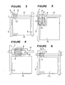
- the source electrode may be formed in such a manner that as shown in Figure 3, the first source electrode 7 is connected to the source connecting electrode 9 as well as the second source electrode 8. This construction is advantageous in that a defect in either source electrode is to be repaired.
- a coplanar structure type thin film transistor may be formed as shown in Figure 4. Namely, two source electrodes 7, 8 are extended at the right angle from the source bus line 3, and the drain electrode 10 is interposed between the source electrodes 7, 8.
- the coplanar structure type thin film transistor may be formed in such a manner that the drain electrode 10 is interposed between the source bus line 3 and the source electrode 8 extended in parallel to the source bus line 3 as shown in Figure 5.
- the drain electrode receives a source signal from the remaining source electrode 8 or 7.
- the thin film transistor has a sufficient capability.
- a color tone is somewhat different from the inherent color tone.
- the difference between them is not recognizable in a case of a moving picture and the value of a picture image is remarkably improved in comparison with that of the conventional thin film transistor having a line defect.
- Figure 9 is a plane view of a modified embodiment of the thin film transistor having a simplified pattern in which two source electrodes 7', 8 are formed and the source electrode 7' is electrically separated from the source bus line 4.
- the source electrode 8 of the thin film transistor is separated at its root portion 18, and the other source electrode 7' which is electrically separated is connected to the source connecting electrode at a portion indicated by a numeral 19 whereby the function of the transistor is recovered.
- the picture element repaired is subjected to influence of the stray transistor.
- the repaired picture element has the same effect as described above.
- the method of repairing the thin film transistor is applicable to the coplanar structure type and the staggered structure type.
- FIG 11 shows the sixth embodiment of the present invention.
- the thin film transistor has a three drain electrodes 10, 35, 38, each of which is interposed between each pair of source electrodes 7, 8; 34, 36; 37, 39.
- the performance of the thin film transistor is insufficient, it is effective to use a plurality of the thin film transistors having the structure as shown in Figure 11. Namely, by ar ranging the plurality of the thin film transistors, thi intensity of a drain current is multipled by the number of transistors used. Thus, the drain curren required to display can be obtained.
- a method of repairing the thin film transisto having the above-mentioned structure will be de scribed with reference to Figure 12.
- any defect is found in the thin film transistor, it i: possible to repair the thin film transistor by cuttinc the drain electrode and/or the source electrode to electrically separate them.
- the source elec. trode 34 and the drain electrode 35 are respectively cut at positions shown by numerals 18, 21 respectively. Namely, among three transistors when one thin film transistor having the defect i: separated, a drain current having the current inten.
- Figure 13 shows the seventh embodiment which is applicable to the thin film transistor under the condition that the performance of the transistor is sufficient.
- a plurality. of thin film transistors are provided for a single picture elemeni 15 in which a plurality of drain electrodes are placed between two source electrodes.
- Two thin film transistors 24 each having a pair of source electrodes and a drain electrode are electrically separated from the source bus line and the picture element displaying electrode 15.
- the two thin film transistors 24 are auxiliary transistors which are electrically separated from each other and the other electrodes.
- the drain and/or source electrodes of the transistor 23 are cut at portions indicated by numeral 18, 21 so that these electrodes are electrically separated: the source electrodes of the auxiliary thin film transistor 26 which is near the main thin film transistor 23 and is in an electrically insulated state are connected to the source connecting electrode by a bridge member 25, and the drain electrode of the transistor 26 is connected to the picture element displaying electrode 15 by a bridge member 19 respectively; thus the thin film transistor 26 connected becomes operative.
- the drain current supplied to the picture element displaying electrode 15 is unchanged since the number of picture elements including normal picture elements and the repaired picture elements is unchanged. Further, the picture element displaying electrode 15 ean receive a normal source signal. Accordingly, the display apparatus without no defect can be obtained.
- the number of -the thin film transistors is not limited to that in the above-mentioned embodiment.
- the number of the drain and source electrodes electrically separated is also not limited to the above-mentioned embodiment.
- a method of cutting the electrodes to repair the thin film transistor may be any suitable method such as a method by using a laser trimmer, an ultrasonic cutter so on.
- any suitable method can be utilized. For instance, a small conducting material is placed to the portion to be bridged by means of a dispenser, or a glass base plate coated with gold or alminum is placed on the thin film transistor base plate and a laser beam focused to be a predetermined size is irradiated under the atmospheric pressure or a reduced pressure from the side of the metal coated base plate so that a metal is coated on a desired portion of the thin film transistor base plate (the method being referred to as a , laser coating method).
- a liquid crystal display device is manufactured in such a manner that a base plate having thin film transistors produced or repaired as described above and another base plate with electrodes to be opposed to the base plate having transisters are prepared; an overcoat layer of a material such as polyimide, polyamide, silica, almina and so on is formed on the surface of the base plate with electrodes, followed by rubbing the surface to form an oriented film layer, if necessary; the two base plates are arranged so that their surfaces with the electrodes are opposed with a gap in the range of about 1 ⁇ m -about 20 am; the peripheral parts of the two base plates are sealed; and then, a liquid crystal is enclosed between the base plates.
- a material such as polyimide, polyamide, silica, almina and so on
- a color filter layer or a light shielding layer is formed on or below the electrodes; a spacer member such as plastic balls, glass fibers, ceramic balls is interposed between the base plates to control the gap formed therebetween; a dichroic dye is mixed to the liquid crystal to effect color display; or a polirizer film, a reflecting film or an illumination means is disposed outside the liquid crystal display apparatus.
- the picture element displaying electrode 15 When the source bus line 3 or 4 is at low electric potential the picture element displaying electrode 15 is also maintained to be a low potential. Accordingly, the liquid crystal switch is not turned on and the picture element corresponding to the picture element displaying electrode 15 is in a non-operated condition.
- the source electrodes 7, 8 are electrically separated from the drain electrode 10, and the liquid crystal switch for the picture element ' corresponding to the picture element displaying electrode 15 is kept in the original state due to the capacitance of the liquid crystal or an additional capacitance.
- the ratio of the channel width to the channel length (W/L) is large and the drain electrode 10 is electrically separated from the n + 1 th source bus line 5 by means of the second source electrode 8. Accordingly, a sufficient drain current can be obtained. Further, there is no problem of formation of a stray transistor by the drain electrode 10 in association with the n + 1 th source bus line 5. Thus, there is obtainable good switching operation.
- the source electrode 7 or 8, and/or the gate electrode 12 are separated from the source bus line 3 or 4, or the gate bus line at the portion indicated by the reference numeral 18 to recover normal switching operation of the thin film transistor.
- the same switching operation can be obtained even when only one source electrode 8 is connected to the source bus line 4.
- the source electrode 8 is separated from the source bus line 4, and the auxiliary source electrode 7' is connected to the source bus line 4 so that normal switching operation is attained.
- a sufficient drain current can be obtained and therefore excellent displaying effect is obtainable by providing a plurality of drain electrodes 10, 35, 38 and by interposing each of the drain electrodes between each pair of source electrodes 7, 8; 34, 36; and 37, 39.
- the thin film transistor of the present invention is so formed that when a defect is found in structural elements of a picture element for display, repairing can be made so as to apply a voltage from a source bus line inclusively used for the picture element. Accordingly, the thin film transistor capable of complete deletion or repair of the defects is obtainable. Accordingly, it is more effective than the conventional thin film transistor in which a voltage is applicable only from the adjacent source bus line when a defect is found.
- n + a-Si amorphous silicon
- a-Si, 2000 A SiON film were coated with P-CVD (plasma chemical vapor deposi. tion) followed by coating aluminum layer of a thick. ness of 3000 A to form gate electrodes.
- P-CVD plasma chemical vapor deposi. tion
- aluminum layer of a thick. ness of 3000 A By using photoresist method, the layers of aluminum, a-S and SiON were etched with the pattern of the gate electrode 12. Then, the n + a-Si layer on the ITC was etched to form thin film transistors for 200 200 picture elements.
- the value o the drain current is twice as much as that in the conventional thin film transistors having a simplifiec pattern. Further, the thin film transistor characteris. tics of a picture element was not influenced by signal of an adjacent source bus line at all.
- a liquid crystal display panel was assemblec by coating an orientated film of polyimide on the , base plate, and inspection of activation on the panel was carried out. in the gradation display operation, a clear and correct picture image coulc be obtained. There were found four activated line defects due to the leakage between the source anc the gate and two activated point defects due to the leakage between the gate and the drain.
- a thin film structure was prepared as in the same manner as in Example 1 except that each oi the drain electrodes 10 was interposed between each pair of source electrodes 7, 8 connected tc each of the source connecting electrodes 9 as shown in Figure 3. Inspection was carried out on the thin film transistors thus prepared. There were found three defects of the leakage between the source and the gate and only one defect of the leakage between the gate and the drain.
- a liquid crystal display panel was prepared in the same manner as the Example 1, and inspection of activation was carried out. There was no activated point defect due to the leakage between the _ journeyce and the gate, but only one defect- of activated point defect due to the leakage between the gate and the drain was found.
- the repaired picture element shows low contrast in comparison with other normal picture elements.
- a thin film structure was prepared in the same manner as in the Example 1 except that as shown in Figure 13, three thin film transistors were provided for each of the picture elements, each of the thin-film transistors provided with the single drain electrode 10 interposed between the two source electrodes 7, 8 which were connected to the source connecting electrode 9; the source electrodes 7, 8 and the drain electrode 10 of the thin film transistor 23 nearest to the source bus line 4 were respectively connected to the source bus line 4 and the picture element displaying electrode 15, and the source and drain electrodes of the other thin film transistors 24 are in an electrically insulated state.
- the source electrodes and the drain electrode having the defects were respectively cut as indicated by the reference numerals 18, 21 in Figure 14 from the source connecting electrode 9 and the picture element displaying electrode 15 by using the laser trimmer. Then, 'the source connecting electrode and the drain electrode of the first auxiliary thin film transistor 26 which were electrically separated from any of the electrodes were respectively connected to the source connecting electrode 9 and the picture element displaying electrode 15.
- the laser trimmer was focused to the portions to be connected and glass base plates coated with gold to have a thickness of 5000 A were placed on the thin film transistor base plate with the gold-coated surface facing the base plate, followed by irradiation of a laser beam under a reduced pressure.
- gold on the glass base plates which was subjected to the irradiation of the laser beam was evaporated and deposited on the thin film transistor base plate as shown by the reference numerals 19, 25 in Figure 14, and the source and drain electrodes of the first auxiliary thin film transistor 26 were connected to the source bus line and the picture element displaying electrode.
- the thin film transistors repaired were again subjected to inspection.
- the inspection revealed a defect of the leakage between the source and the gate of the first auxiliary thin film transistor 26.
- the source electrode of the first auxiliary thin film transistor 26 was cut as shown by the reference numeral 18 in Figure 15 by using the same method as described before, followed by connecting-the source connecting electrode and the drain electrode of the second auxiliary thin film transistor 27 to the source connecting electrode of the first auxiliary thin film transistor 26 and the picture element displaying electrode 15 respectively as shown by the reference numerals 25, 22.
- a normal drain current was supplied to the picture element displaying electrode 15 from the second auxiliary thin film transistor 27.
- a liquid crystal display panel was prepared by incorporating the repaired thin film transistors, and inspection of activation was carried out. No point defect and no line defect was recognized even by careful observation.
- a sufficient drain current can be provided by forming the drain electrode between the two source electrodes, and the drain electrodes is not influenced by the stray transistor at all.
- any of the auxiliary thin film transistors can be used to feed a correct source signal to the picture element displaying electrode. Accordingly, a thin film transistor base plate without defects can be prepared; productivity of the thin film transistor base plate is increased, at the cost for manufacturing a display apparatus can be reduced.
- a voltage can be applied to the picture element displaying electrode from the same source bus line which was used before repairing. Accordingly, the trace of repairing is not conspicuous.
- the thin film transistor having the basic structure as shown in Figures 1 to 3, there is an advantage of good productivity since it is sufficient to use two masks, while there is no influence from an adjacent source bus line. Further, as shown in Figures 6, 9 to 14, the thin film transistor allows easy repairing even though there is a defect in the thin film transistor. As shown particularly in Figures 13 and 14, when a thin film transistor without electrical connection to the electrodes is formed and if a defect is found in the thin film transistor having connection to the electrodes, an auxiliary thin film transistor can be used whereby the picture element having the same level as the other normal picture elements can be obtained.
- the gate insulator may be made broader than the width of the gate electrode in order to avoid a problem such that side surfaces of the gate electrode and the source electrode or the drain electrode are damaged by spacers arranged in the liquid crystal cell to cause a short circuit.
- an additional mask is required.
- the number of the masks used in these type transistor is smaller than those used for the coplanar structure type or staggered structure type thin film transistor.
Abstract
Description
- The present invention relates to a thin film transistor for applying a voltage to a picture element displaying electrode for a picture displaying apparatus such as a liquidlctystal type displaying apparatus.
- Requirements of developing a thin display apparatus such as a terminal unit for an office automation apparatus, a plane television receiver and so on have increased. For instance, an active matrix type liquid crystal display apparatus in which electrodes are arranged in a parallel line pattern and active devices are disposed at each intersecting part of the electrodes to activate a liquid crystal, has widely been studied.
- Figure 16 is an equivalent circuit showing a typical active matrix type liquid crystal display apparatus. In Figure 16, a
reference numeral 28 designates a liquid crystal layer and anumeral 29 designates a capacitor which stores a potential applied to the liquid crystal layer. Thecapacitor 29 may be omitted. Anumeral 30 designates a switching transistor for controlling a voltage for actuating the liquid crystal layer. Symbols X,, X2, X3 ... designate selected data lines for controlling the gate of each of theswitching transistors 30 and symbols Y,, Y2, Y3 ... designate data lines for applying a voltage required to actuate the liquid crystal, the data line being driven for each line at a time. - On the other hand, the construction of the thin film transistor used as the switching transistor is classified into a coplanar structure type and a staggered structure type depending on a relation in position of a semiconductor layer, a gate electrode, a source electrode and a drain electrode. Figure 17 is a cross-sectional view of the thin film transistor of the coplanar structure type; Figure 18 is a cross-sectional view of the thin film transistor of the staggered structure type, and Figure 19 is a plane view of the staggered structure type thin film transistor. In Figures 17 to 19, the same reference numerals designate the same structural elements of the thin film transistor. A
reference numeral 1 designates an insulating base plate such as quartz, glass and so on, on which thin film transistors are formed. Anumeral 2 designates a semiconductor layer made of polysilicon, amorphous silicon, CdSe and so on.Numerals numeral 12 designates a gate electrode having patterning by Al, Cr and so on. Anumeral 31 designates a passivation film, a nu.meral 14 designates a contact hole, and anumera 15 designates a picture element displaying electrode made of a transparent conductive film. - It is known a thin film transistor having a sim. plified pattern as shown in a plane view of Figure 20. The thin film transistor as shown in Figure 20 is prepared by forming
source bus lines drain electrode 10 and the picture element display.ing electrode 15 by using the transparent conductive film followed by sequentially forming a semi. conductor layer, an insulating film and thegate electrode 12 in a film form, and then, by etching the laminated body into a pattern of the gate elec.trode 12. - By arranging the thin film transistor having the above-mentioned structure for each picture elements, there is obtainable a high content information display apparatus having a high picture quality in comparison with a conventional apparatus having a panet formed by a dot matrix system. Thus, a high content liquid crystal display apparatus having a high picture quality can be obtained by using the thin film transistors.
- In such display apparatus, a single picture element requires a thin film transistor. Accordingly, ii is necessary to arrange 120 thousands thin film , transistors on a single base plate to prepare a display panel having electrodes of 600 lines x 200 rows. It is very difficult to install a great number oi thin film transistors without any fault. '
- In the transistors, there are many kinds oi troubles of defects such as open circuit of a gate or a source, leakage between a gate and a source, leakage between a gate and a drain, leakage between a source and a drain, poor transistor property and so on.
- The open circuit of the gate or the source derives from a scratch in the manufacturing steps and a defect of stepcoverage of the crossover portion of the transistor. These defects cause a non-activated line defect when the transistor is used in a liquid crystal cell. It is, however, possible that the transistor is repaired by connecting lead- out electrodes at both ends of a disconnected line.
- On the other hand, the leakage between the gate and the source is resulted from dust entering in the insulator. Due to the leakage, a gate signal continuously escapes to a source line through a point of short circuit, and a voltage is always applied to the source thereby causing an activated line defect.
- The leakage between the gate and the drain is resulted from the similar cause. In this case, a gate voltage is applied to the drain through a point of short circuit irrespective of presence of the source signal. In this case, an activated point defect also takes place. Further, when the transistor property is poor and application of a gate vottage do not pass a sufficient current, a source signal voltage is not applied to the transistor thereby causing a non-activated point defect in selecting operation.
- The leakage between the source and the drain occurs due to presence of an extra pattern of etching of the source-drain electrode. In this case, a source signal is usually applied to the drain electrode to thereby cause an activated point defect.
- In inspection of the defects of the thin film transistors by using a microscope, the defects are, in almost case, due to a foreign substance, a pin hole, an extra pattern of etching.
- Occurrence of the defects depends on a manner of controlling of a process. Any line defect is not permissible in display elements. The point defect should be about 0.01 % or smaller. However, in the base plate having 200 or more lines, there are a few line defects and the point defects in the range from 0.1% to 3%. Accordingly, productivity of the liquid crystal cell is low whereby practical use of the active matrix type picture display apparatus is hindered.
- The number of defects can be reduced by reducing the number of processes for preparing the thin film transistor. The thin film transistor of a simplified pattern is produced by two masks as shown in Figure 20, which effectively reduces occurrence of the defects. However, in the thin film transistor produced by the simplified process, a drain current undergoes influence of a
switching transistor 30 and astray transistor 32. Theswitching transistor 30 is formed by the n thsource bus line 4 and thedrain electrode 10 as shown in Figure 20. The characteristics of theswitching transistor 30 is determined by the channel width/the channel length = W/L, where the distance between thesource bus line 4 and thedrain electrode 10 is L, and the width of thegate electrode 12 is W. Thestray transistor 32 is formed by the n + 1 thsource bus line 5 and thedrain electrode 10 and the characteristics of the transistor.32 is determined by the channel width/the channel length = W/L, where the distance between thesource bus line 5 and thedrain electrode 10 is L,. The intensity of the drain current caused by thestray transistor 32 depends on a designed value of the thin film transistor. Usually, it is about 5% -20% as large as a current value caused by the switching transistor. The value does not raise a big problem in a case of a binary display system. However, in a gradation display system, a signal flowing in the adjacent source line is picked up whereby a clear display can not be obtained. - Further, there was a problem that a current sufficient to activate the picture elements is not provided since the size of the transistor is small in comparison with the surface area of the picture elements.
- It is an object of the present invention to eliminate the disadvantages of the conventional thin film transistor and to provide a thin film transistor which provides good productivity when a number of thin film transistors are formed on a single insulating base plate, has a simple structure without being subjected to influence of a stray transistor and other elements, and is capable of showing an excellent picture image when it is used for a picture display apparatus.
- According to the present invention, there is provided a thin film transistor connected to a picture element displaying electrode formed on an insulating base plate so that a voltage is applied to the electrode, characterized by comprising a gate electrode, one or more drain electrodes connected to the picture element displaying electrode, and a source bus line which applies a voltage to one or more source electrodes connected thereto, wherein the one drain electrode is formed between the source bus line which functions by itself as a source electrode and the one source electrode connected to the source bus line, or between the source electrodes. adjacent to each other, which are connected to the source bus line.
- As an another aspect of the present invention, there is provided a method of repairing a thin film transistor connected to a picture element displaying electrode formed on an insulating base plate so that a voltage is applied to the electrode, wherein the thin film transistor comprising a gate electrode, at least two drain electrodes connected to the picture element displaying electrode, a source bus line, a plurality of source electrodes connected to the source bus line which applies a voltage to the source electrodes, and wherein the drain electrodes are formed between the source bus line which functions itself as a source electrode and one of the source electrodes, or between the source electrodes adjacent to each other, each of which is other than the source bus line as a source electrode, characterized-in that a faulty portion of any electrode is separated from the source bus line or the picture element displaying electrode, and another set of the drain electrode and the source electrodes is connected to the source bus line and the picture element displaying electrode, if necessary.
- As still another aspect of the present invention, there is provided a display apparatus comprising an insulating base plate on which a plurality of thin film transistors are formed to be connected to a picture element displaying electrode so that a voltage is applied to the electrode, and a liquid crystal contained between the base plate and -electrode, characterized in that each of the thin film transistors comprises a gate electrode, one or more drain electrodes connected to the picture element displaying electrode, one or more source electrodes and a source bus line connected to the one or more source electrodes to apply a voltage to the source electrodes, wherein the drain electrode is interposed between the source bus line which functions by itself as a source electrode and the one source electrode connected to the source bus line, or between source electrodes adjacent to each other connected to the source bus line.
- In drawing:
- Figure 1 is a plane view showing an embodiment of the thin film transistor according to the present invention;
- Figure 2 is a cross-sectional view taken along a line AA' in Figure 1;
- Figure 3 is a plane view of another embodiment of the thin film transistor according to the present invention;
- Figures 4 and 5 are respectively plane views showing the third and the fourth embodiments of the thin film transistor of the present invention;
- - Figures 6, 7 and 8 are respectively plane views showing how to repair the defect of leakage between the source and the gate of the thin film transistor of the present invention;
- Figure 9 is a plane view showing the fifth embodiment of the thin film transistor of the present invention;
- Figure 10 is a plane view showing how to repair the defect of leakage between the source and the gate of the thin film transistor shown in Figure 9;
- Figure 11 is a plane view showing sixth embodiment of the thin film transistor of the present invention;
- Figure 12 is a plane view showing how tc repair a faulty portion in the thin film transistor as shown in Figure 11;
- Figure 13 is a plane view showing the seventh embodiment of the thin film transistor of the present invention;
- Figure 14 is a plane view showing how to repair a faulty portion in the thin film transistor as shown in Figure 13;
- Figure 15 is a plane view showing how to repair the thin film transistor of the present invention when a faulty portion has been further found in the repaired transistor;
- Figure 16 is an equivalent circuit of a conventional active matrix type liquid crystal display apparatus;
- Figure 17 is a cross-sectional view of a conventional coplanar type thin film transistor;
- Figure 18 is a cross-sectional view of a conventional inverted staggered type thin film, transistor;
- Figure 19 is a plane view of the conventional inverted staggered type thin film transistor; and
- Figure 20 is a plane view of a conventional thin film transistor having a simplified pattern.
- In the following, preferred embodiments of the thin film transistor according to the present invention will be described with reference to the drawings.
- Figure 1 is a plane view showing the first embodiment of the present invention and Figure 2 is a cross-sectional view taken along a line AA' in Figure 1.
- An insulating base plate is made of an insulating material such as quartz, glass and so on. An electrode of transparent conductive film made of, for instance, an indium-tin oxide (ITO) is formed on a surface of the baseplate. n and P type semiconductor layers 16 which are respectively formed by doping an element such as P, As and so on or an element such as B and so on in a semiconductor material -such as polysilicon, amorphous silicon, CdSe and so on is coated on the electrode.
- The doped semiconductor layers 16 and the transparent electrode formed on the insulating base plate are simultaneously subjected to a patterning operation thereby to form a picture element display electrode 15 a
source bus line 4, thesecond source electrode 8, asource connecting electrode 9 and adrain electrode 10 as shown in Figure 1. In an area near the upper left comer portion of the pictureelement displaying electrode 15 in Figure 1, there are formed thesecond source electrode 8 in substantially parallel to thesource bus line 4 and thesource connecting electrode 9 for connecting thesecond source electrode 8 to thesource bus line 4. Also, at the upper left comer portion of the pictureelement displaying electrode 15, thedrain electrode 10 is formed so that it extends between thesource bus line 4 and thesecond source electrode 8. - A
semiconductor layer 2 of a semiconductor material such as polysilicon, amorphous silicon, CdSe and so on, a gate insulator 11 made of a insulating material such as 8i02, Si,N.. SiON and so on and a metallic layer used for a gate electrode which is made of a material such as Al, Cr and so on are sequentially formed on the base plate in this order. Then, the laminated body is subjected to sequentially etching operations of the metallic layer, the gate insulator and the semiconductor layer with a pattern of thegate electrode 12 as shown in Figure 1, whereby thegate electrode 12, the gate insulator 11 and thesemiconductor layer 2 are formed. Then, the doped semiconductor layer on the source bus line and other electrodes which are exposed in the area other than the gate electrode pattern is also removed by etching. - A portion between the
source bus line 4 and thegate electrode 12 which spatially intersect with each other functions as thefirst source electrode 7. - Thus, a source signal is supplied to the
drain electrode 10 from the first andsecond source electrodes - In this case, the
drain electrode 10 is electrically isolated from the n + 1 thsource bus line 5 by means of thesecond source electrode 8. Accordingly, no stray transistor is formed with respect to the n + 1 thsource bus line 5, and only signal of the n thsource bus line 4 is supplied to the pictureelement displaying electrode 15, whereby correct display can be obtained. - The source electrode may be formed in such a manner that as shown in Figure 3, the
first source electrode 7 is connected to thesource connecting electrode 9 as well as thesecond source electrode 8. This construction is advantageous in that a defect in either source electrode is to be repaired. - In the foregoing, description has been made as to the thin film transistor having a simplified pattern. However, the present invention is not limited to the thin film transistor having such pattern and structure, but is applicable to the conventional coplanar type or staggered type thin film transistor. For instance, a coplanar structure type thin film transistor may be formed as shown in Figure 4. Namely, two
source electrodes source bus line 3, and thedrain electrode 10 is interposed between thesource electrodes drain electrode 10 is interposed between thesource bus line 3 and thesource electrode 8 extended in parallel to thesource bus line 3 as shown in Figure 5. In the coplanar structure type and staggered structure type thin film transistors, there is no influence by the stray transistor as is in the conventional thin film transistor having the simplified pattern. However, in the structure as shown in Figures 4 and 5 according to the present invention, there is an advantage that the ratio of the channel width to the channel length (W/L) of the thin film transistor is twice as much as that in the conventional transistor, and effective measures can be easily taken when there is a defect in the transistor. - In the following, description will be made as to a method of repairing of a defect in the thin film transistor when the defect is found. In extensive study of a great number of thin film transistors on the base plate, the inventors of the present application have found that positions where various defects may occur are indefinite in the base plate and possibility of occurrence defects in the neighbouring thin film transistors is extremely low. The present invention has been attained in view of the fact. Among the above-mentioned defects, a defect of the leakage between the source and the gate indicates the highest possibility. The leakage between the source and the gate invites a serious activated line defect which is the main cause of low productivity.
- On the other hand, under the condition that a thin film transistor has good characteristics; a sufficient drain current can be obtained even in the structure having a small W/L ratio, and a leakage as shown by a numeral 17 exists in only one of two source-gate overlapping portions (Figures 6, 7 and 8), the
source electrode gate electrode 12 can be separated by any suitable way as shown by a numeral 18. - In this case, the drain electrode receives a source signal from the remaining
source electrode - Figure 9 is a plane view of a modified embodiment of the thin film transistor having a simplified pattern in which two
source electrodes 7', 8 are formed and the source electrode 7' is electrically separated from thesource bus line 4. In this embodiment, when a defect of the leakage between the source and the gate as indicated by a numeral 17 in Figure 10 is found by an inspection, thesource electrode 8 of the thin film transistor is separated at itsroot portion 18, and the other source electrode 7' which is electrically separated is connected to the source connecting electrode at a portion indicated by a numeral 19 whereby the function of the transistor is recovered. In a case that thesecond source electrode 8 which is placed near the adjacentsource bus line 5 is cut, the picture element repaired is subjected to influence of the stray transistor. However, it is difficult to discriminate the repaired picture elements which are scattered in a great number of picture elements. The repaired picture element has the same effect as described above. - The method of repairing the thin film transistor is applicable to the coplanar structure type and the staggered structure type.
- In the next place, description will be made as to a thin film transistor of a simplified pattern having a plurality of drain electrodes.
- Figure 11 shows the sixth embodiment of the present invention. The thin film transistor has a three
drain electrodes 10, 35, 38, each of which is interposed between each pair ofsource electrodes - A method of repairing the thin film transisto having the above-mentioned structure will be de scribed with reference to Figure 12. When any defect is found in the thin film transistor, it i: possible to repair the thin film transistor by cuttinc the drain electrode and/or the source electrode to electrically separate them. For instance, when
defect 17 of the leakage between the source anc the gate in the source electrode 34 and a defect 2( of the leakage between the gate and the drain ir the drain electrode 35 are found, the source elec. trode 34 and the drain electrode 35 are respectively cut at positions shown bynumerals electrode 15. In this case, difference ir display characteristic between the picture element having the defect electrode and other normal picture elements becomes small in comparison witt the embodiment shown in Figure 10, and a picture image having a high quality can be obtained. - Figure 13 shows the seventh embodiment which is applicable to the thin film transistor under the condition that the performance of the transistor is sufficient. In Figure 13, a plurality. of thin film transistors are provided for a single picture elemeni 15 in which a plurality of drain electrodes are placed between two source electrodes. Two
thin film transistors 24 each having a pair of source electrodes and a drain electrode are electrically separated from the source bus line and the pictureelement displaying electrode 15. In more detail, the twothin film transistors 24 are auxiliary transistors which are electrically separated from each other and the other electrodes. When any defect is found in the mainthin film transistor 23, the drain and/or source electrodes of thetransistor 23 are cut at portions indicated bynumeral thin film transistor 26 which is near the mainthin film transistor 23 and is in an electrically insulated state are connected to the source connecting electrode by abridge member 25, and the drain electrode of thetransistor 26 is connected to the pictureelement displaying electrode 15 by abridge member 19 respectively; thus thethin film transistor 26 connected becomes operative. - In the thin film transistors having the above-mentioned structure, the drain current supplied to the picture
element displaying electrode 15 is unchanged since the number of picture elements including normal picture elements and the repaired picture elements is unchanged.. Further, the pictureelement displaying electrode 15 ean receive a normal source signal. Accordingly, the display apparatus without no defect can be obtained. - In the present invention, the number of -the thin film transistors is not limited to that in the above-mentioned embodiment. The number of the drain and source electrodes electrically separated is also not limited to the above-mentioned embodiment.
- A method of cutting the electrodes to repair the thin film transistor may be any suitable method such as a method by using a laser trimmer, an ultrasonic cutter so on.
- When the drain electrode of the second transistor is connected to the picture element displaying electrode, any suitable method can be utilized. For instance, a small conducting material is placed to the portion to be bridged by means of a dispenser, or a glass base plate coated with gold or alminum is placed on the thin film transistor base plate and a laser beam focused to be a predetermined size is irradiated under the atmospheric pressure or a reduced pressure from the side of the metal coated base plate so that a metal is coated on a desired portion of the thin film transistor base plate (the method being referred to as a , laser coating method).
- A liquid crystal display device is manufactured in such a manner that a base plate having thin film transistors produced or repaired as described above and another base plate with electrodes to be opposed to the base plate having transisters are prepared; an overcoat layer of a material such as polyimide, polyamide, silica, almina and so on is formed on the surface of the base plate with electrodes, followed by rubbing the surface to form an oriented film layer, if necessary; the two base plates are arranged so that their surfaces with the electrodes are opposed with a gap in the range of about 1 µm -about 20 am; the peripheral parts of the two base plates are sealed; and then, a liquid crystal is enclosed between the base plates. In addition to the manufacturing steps as above-mentioned, it is possible to employ such a process, as in a conventional liquid crystal display apparatus, that a color filter layer or a light shielding layer is formed on or below the electrodes; a spacer member such as plastic balls, glass fibers, ceramic balls is interposed between the base plates to control the gap formed therebetween; a dichroic dye is mixed to the liquid crystal to effect color display; or a polirizer film, a reflecting film or an illumination means is disposed outside the liquid crystal display apparatus.
- In the embodiments as shown in Figures 1 to 5, when a high voltage is applied to the
gate electrode 12, a current flows into thedrain electrode 10 through the first andsecond source electrodes source bus line semiconductor layer 2 whereby the pictureelement displaying electrode 15 connected to thedrain electrode 10 becomes the same potential as thesource bus line source bus line element displaying electrode 15 and a common electrode (not shown). In a case of the liquid crystal display apparatus, a liquid crystal switch placed between the pictureelement displaying electrode 15 and the common electrode is turned on so that the picture element corresponding to the pictureelement displaying electrode 15 is operated for display. - When the
source bus line element displaying electrode 15 is also maintained to be a low potential. Accordingly, the liquid crystal switch is not turned on and the picture element corresponding to the pictureelement displaying electrode 15 is in a non-operated condition. - While a selected potential is applied to other gate electrodes, a low potential is supplied to the
gate electrode 12 which has received a signal so that thesemiconductor layer 2 has a high resistance. Accordingly, thesource electrodes drain electrode 10, and the liquid crystal switch for the picture element ' corresponding to the pictureelement displaying electrode 15 is kept in the original state due to the capacitance of the liquid crystal or an additional capacitance. - In the embodiments shown in Figures 1 to 5, the ratio of the channel width to the channel length (W/L) is large and the
drain electrode 10 is electrically separated from the n + 1 thsource bus line 5 by means of thesecond source electrode 8. Accordingly, a sufficient drain current can be obtained. Further, there is no problem of formation of a stray transistor by thedrain electrode 10 in association with the n + 1 thsource bus line 5. Thus, there is obtainable good switching operation. In a method of repairing the thin film transistor as shown in Figures 1 to 5, when adefect 17 of the leakage between the source and the gate as shown in Figures 6 to 8 takes place, thesource electrode gate electrode 12 are separated from thesource bus line reference numeral 18 to recover normal switching operation of the thin film transistor. - As shown in Figures 9 and 10, the same switching operation can be obtained even when only one
source electrode 8 is connected to thesource bus line 4. In this case, when adefect 17 of the leakage between the source and the gate takes place in thesource electrode 8, thesource electrode 8 is separated from thesource bus line 4, and the auxiliary source electrode 7' is connected to thesource bus line 4 so that normal switching operation is attained. - In the embodiment shown in Figure 11, a sufficient drain current can be obtained and therefore excellent displaying effect is obtainable by providing a plurality of
drain electrodes 10, 35, 38 and by interposing each of the drain electrodes between each pair ofsource electrodes - As shown in Figure 12, defeets of the
leakage 17 between the source and the gate and/or the leakage 20 between the gate and the drain are found, the source electrode 34 and the drain electrode 35 having the defects are separated from the source bus line and the picture element displaying electrode at the portions indicated by thenumerals - In the embodiment shown in Figure 13 in which two auxiliary
thin film transistors 24 are provided, the same repairing method as in the foregoing embodiments can be employed. In this case, the same quantity of the drain current as that before repairing can be obtained and accordingly, a stable display effect can be obtained. - Thus, the thin film transistor of the present invention is so formed that when a defect is found in structural elements of a picture element for display, repairing can be made so as to apply a voltage from a source bus line inclusively used for the picture element. Accordingly, the thin film transistor capable of complete deletion or repair of the defects is obtainable. Accordingly, it is more effective than the conventional thin film transistor in which a voltage is applicable only from the adjacent source bus line when a defect is found.
- In the following, examples of manufacturing and repairing of the thin film transistor according to the present invention will be described.
- On a glass base plate of 50 mm square indium-tin oxide layer of 1000 Å thick and n' amorphous silicon (n+a-Si) of 500 A were coated Then, the
source bus lines con necting electrodes 9, thesource electrodes 8, thedrain electrodes 10 and the picture elementdis playing electrodes 15 were formed in a predeter mined pattern as shown in Figure 1. Thedrair electrodes 10 were formed to be put between thesource electrodes - Then, 2000 A a-Si, 2000 A SiON film were coated with P-CVD (plasma chemical vapor deposi. tion) followed by coating aluminum layer of a thick. ness of 3000 A to form gate electrodes. By using photoresist method, the layers of aluminum, a-S and SiON were etched with the pattern of the
gate electrode 12. Then, the n+a-Si layer on the ITC was etched to form thin film transistors for 200 200 picture elements. - In measuring the characteristics of the thin filrr transistors formed on the base piste, the value o the drain current is twice as much as that in the conventional thin film transistors having a simplifiec pattern. Further, the thin film transistor characteris. tics of a picture element was not influenced by signal of an adjacent source bus line at all.
- A liquid crystal display panel was assemblec by coating an orientated film of polyimide on the , base plate, and inspection of activation on the panel was carried out. in the gradation display operation, a clear and correct picture image coulc be obtained. There were found four activated line defects due to the leakage between the source anc the gate and two activated point defects due to the leakage between the gate and the drain.
- A thin film structure was prepared as in the same manner as in Example 1 except that each oi the
drain electrodes 10 was interposed between each pair ofsource electrodes source connecting electrodes 9 as shown in Figure 3. Inspection was carried out on the thin film transistors thus prepared. There were found three defects of the leakage between the source and the gate and only one defect of the leakage between the gate and the drain. - In observation of the thin film transistors having the three defects Qf the leakage between the source and the gate, black foreign substances were found at two intersecting portions in the
gate electrode 12 and thefirst source electrode 7, and a intersecting portion in thegate electrode 12 and thesecond source electrode 8. The root portion of the source electrode having the foreign substance was cut by a laser trimmer as indicated by thereference numeral 18 in Figure 6 to electrically separate the source electrode from thesource connecting electrode 9 and thesource bus line 4. - A liquid crystal display panel was prepared in the same manner as the Example 1, and inspection of activation was carried out. There was no activated point defect due to the leakage between the _jource and the gate, but only one defect- of activated point defect due to the leakage between the gate and the drain was found.
- In careful observation of the repaired picture- element at a close distance, the repaired picture element shows low contrast in comparison with other normal picture elements. However, when the repaired picture element is observed at a distance of 30 cm, difference between the repaired picture element and the other elements could not be recognized. Accordingly, it was understood that there was no problem as a picture element=
- A thin film structure was prepared in the same manner as in the Example 1 except that as shown in Figure 13, three thin film transistors were provided for each of the picture elements, each of the thin-film transistors provided with the
single drain electrode 10 interposed between the twosource electrodes source connecting electrode 9; thesource electrodes drain electrode 10 of thethin film transistor 23 nearest to thesource bus line 4 were respectively connected to thesource bus line 4 and the pictureelement displaying electrode 15, and the source and drain electrodes of the otherthin film transistors 24 are in an electrically insulated state. - All the thin film transistors on the base plate were inspected. In the inspection, there were found three defects of the leakage between the source and the gate and two defects of the leakage between the gate and the drain. The source electrodes and the drain electrode having the defects were respectively cut as indicated by the
reference numerals source connecting electrode 9 and the pictureelement displaying electrode 15 by using the laser trimmer. Then, 'the source connecting electrode and the drain electrode of the first auxiliarythin film transistor 26 which were electrically separated from any of the electrodes were respectively connected to thesource connecting electrode 9 and the pictureelement displaying electrode 15. In the connecting operations, the laser trimmer was focused to the portions to be connected and glass base plates coated with gold to have a thickness of 5000 A were placed on the thin film transistor base plate with the gold-coated surface facing the base plate, followed by irradiation of a laser beam under a reduced pressure. With the operations, gold on the glass base plates which was subjected to the irradiation of the laser beam was evaporated and deposited on the thin film transistor base plate as shown by thereference numerals thin film transistor 26 were connected to the source bus line and the picture element displaying electrode. - The thin film transistors repaired were again subjected to inspection. The inspection revealed a defect of the leakage between the source and the gate of the first auxiliary
thin film transistor 26. To remove the defect, the source electrode of the first auxiliarythin film transistor 26 was cut as shown by thereference numeral 18 in Figure 15 by using the same method as described before, followed by connecting-the source connecting electrode and the drain electrode of the second auxiliarythin film transistor 27 to the source connecting electrode of the first auxiliarythin film transistor 26 and the pictureelement displaying electrode 15 respectively as shown by thereference numerals element displaying electrode 15 from the second auxiliarythin film transistor 27. - A liquid crystal display panel was prepared by incorporating the repaired thin film transistors, and inspection of activation was carried out. No point defect and no line defect was recognized even by careful observation.
- In the thin film transistor according to the present invention, a sufficient drain current can be provided by forming the drain electrode between the two source electrodes, and the drain electrodes is not influenced by the stray transistor at all.
- By providing a plurality of thin film transistors, if the main thin film transistor is faulty, any of the auxiliary thin film transistors can be used to feed a correct source signal to the picture element displaying electrode. Accordingly, a thin film transistor base plate without defects can be prepared; productivity of the thin film transistor base plate is increased, at the cost for manufacturing a display apparatus can be reduced.
- Further, after the repairing, a voltage can be applied to the picture element displaying electrode from the same source bus line which was used before repairing. Accordingly, the trace of repairing is not conspicuous.
- In the present invention, by using the thin film transistor having the basic structure as shown in Figures 1 to 3, there is an advantage of good productivity since it is sufficient to use two masks, while there is no influence from an adjacent source bus line. Further, as shown in Figures 6, 9 to 14, the thin film transistor allows easy repairing even though there is a defect in the thin film transistor. As shown particularly in Figures 13 and 14, when a thin film transistor without electrical connection to the electrodes is formed and if a defect is found in the thin film transistor having connection to the electrodes, an auxiliary thin film transistor can be used whereby the picture element having the same level as the other normal picture elements can be obtained.
- In the above-mentioned embodiments, the gate insulator may be made broader than the width of the gate electrode in order to avoid a problem such that side surfaces of the gate electrode and the source electrode or the drain electrode are damaged by spacers arranged in the liquid crystal cell to cause a short circuit. In this case, an additional mask is required. However, the number of the masks used in these type transistor is smaller than those used for the coplanar structure type or staggered structure type thin film transistor.
Claims (10)
Applications Claiming Priority (2)
| Application Number | Priority Date | Filing Date | Title |
|---|---|---|---|
| JP85456/85 | 1985-04-23 | ||
| JP60085456A JPH0740101B2 (en) | 1985-04-23 | 1985-04-23 | Thin film transistor |
Publications (3)
| Publication Number | Publication Date |
|---|---|
| EP0200138A2 true EP0200138A2 (en) | 1986-11-05 |
| EP0200138A3 EP0200138A3 (en) | 1988-01-07 |
| EP0200138B1 EP0200138B1 (en) | 1991-09-25 |
Family
ID=13859382
Family Applications (1)
| Application Number | Title | Priority Date | Filing Date |
|---|---|---|---|
| EP86105497A Expired EP0200138B1 (en) | 1985-04-23 | 1986-04-21 | Thin film transistor, method of repairing the thin film transistor and displaying apparatus having the thin film transistor |
Country Status (4)
| Country | Link |
|---|---|
| US (2) | US4907861A (en) |
| EP (1) | EP0200138B1 (en) |
| JP (1) | JPH0740101B2 (en) |
| DE (1) | DE3681626D1 (en) |
Cited By (13)
| Publication number | Priority date | Publication date | Assignee | Title |
|---|---|---|---|---|
| EP0318224A2 (en) * | 1987-11-19 | 1989-05-31 | Sharp Kabushiki Kaisha | An active matrix substrate for liquid crystal display |
| EP0333151A2 (en) * | 1988-03-18 | 1989-09-20 | Seiko Epson Corporation | Thin film transistor |
| EP0365244A2 (en) * | 1988-10-17 | 1990-04-25 | Sharp Kabushiki Kaisha | An active matrix substrate |
| EP0372898A2 (en) * | 1988-12-06 | 1990-06-13 | Sharp Kabushiki Kaisha | Active matrix display apparatus |
| EP0380265A2 (en) * | 1989-01-23 | 1990-08-01 | Sharp Kabushiki Kaisha | A method of manufacturing active matrix display apparatuses |
| EP0430418A2 (en) * | 1989-11-30 | 1991-06-05 | Kabushiki Kaisha Toshiba | Liquid crystal display and method of manufacturing the same |
| EP0461417A2 (en) * | 1990-05-16 | 1991-12-18 | Hosiden Corporation | Liquid crystal display element and method for treating defective pixels therein |
| US5392143A (en) * | 1989-11-30 | 1995-02-21 | Kabushiki Kaisha Toshiba | Liquid crystal display having drain and pixel electrodes linkable to a wiring line having a potential |
| WO1995012144A1 (en) * | 1993-10-29 | 1995-05-04 | Litton Systems Canada Limited | Repairable bus structure for amlcd array |
| EP2495763A1 (en) * | 2011-03-03 | 2012-09-05 | Samsung Electronics Co., Ltd. | Electronic systems, thin film transistors, methods of manufacturing thin film transistors and thin film transistor arrays |
| US8629440B2 (en) | 2005-01-31 | 2014-01-14 | Semiconductor Energy Laboratory Co., Ltd. | Display device with defective pixels correction structure |
| US8754409B2 (en) | 2011-03-25 | 2014-06-17 | Semiconductor Energy Laboratory Co., Ltd. | Field-effect transistor, and memory and semiconductor circuit including the same |
| US11940697B2 (en) | 2007-05-18 | 2024-03-26 | Semiconductor Energy Laboratory Co., Ltd. | Liquid crystal display device |
Families Citing this family (60)
| Publication number | Priority date | Publication date | Assignee | Title |
|---|---|---|---|---|
| JPH0827464B2 (en) * | 1987-03-05 | 1996-03-21 | 旭硝子株式会社 | Active matrix LCD display |
| JPH07111520B2 (en) * | 1987-05-27 | 1995-11-29 | ホシデン株式会社 | Liquid crystal display element |
| JPS6412577A (en) * | 1987-07-06 | 1989-01-17 | Canon Kk | Thin film transistor |
| JP2850332B2 (en) * | 1988-09-14 | 1999-01-27 | セイコーエプソン株式会社 | Thin film transistor |
| US5243260A (en) * | 1988-11-08 | 1993-09-07 | L'etat Francais, Represente Par Le Ministre Des Postes, Des Telecommunications Et De L'espace (Centre National D'etudes Des Telecommunications) | Method to produce a display screen with a matrix of transistors provided with an optical mask |
| FR2638880B1 (en) * | 1988-11-08 | 1990-12-14 | France Etat | METHOD FOR MANUFACTURING A MATRIX DISPLAY SCREEN WITH TRANSISTORS PROVIDED WITH AN OPTICAL MASK |
| JPH02157828A (en) * | 1988-12-12 | 1990-06-18 | Hosiden Electron Co Ltd | Liquid crystal display element |
| JP2834756B2 (en) * | 1989-01-18 | 1998-12-14 | シャープ株式会社 | Display electrode substrate |
| JP2600929B2 (en) * | 1989-01-27 | 1997-04-16 | 松下電器産業株式会社 | Liquid crystal image display device and method of manufacturing the same |
| US5343216A (en) * | 1989-01-31 | 1994-08-30 | Sharp Kabushiki Kaisha | Active matrix substrate and active matrix display apparatus |
| EP0381428B1 (en) * | 1989-01-31 | 1995-06-21 | Sharp Kabushiki Kaisha | Active matrix substrate and active matrix display display apparatus |
| JP2508259B2 (en) * | 1989-04-13 | 1996-06-19 | 日本電気株式会社 | Superconducting three-terminal element and manufacturing method thereof |
| JP2757207B2 (en) * | 1989-05-24 | 1998-05-25 | 株式会社リコー | Liquid crystal display |
| JP3009438B2 (en) * | 1989-08-14 | 2000-02-14 | 株式会社日立製作所 | Liquid crystal display |
| JPH03121422A (en) * | 1989-10-04 | 1991-05-23 | Nec Corp | Switching element |
| US5037771A (en) * | 1989-11-28 | 1991-08-06 | Cross-Check Technology, Inc. | Method for implementing grid-based crosscheck test structures and the structures resulting therefrom |
| KR920008675Y1 (en) * | 1989-12-30 | 1992-12-12 | 삼성전자 주식회사 | Thin film transistor for plate display |
| JP2514731B2 (en) * | 1990-02-05 | 1996-07-10 | シャープ株式会社 | Active matrix display |
| FR2662290B1 (en) * | 1990-05-15 | 1992-07-24 | France Telecom | METHOD FOR PRODUCING A DISPLAY SCREEN WITH ACTIVE MATRIX AND STORAGE CAPACITORS AND SCREEN OBTAINED BY THIS PROCESS. |
| US5146356A (en) * | 1991-02-04 | 1992-09-08 | North American Philips Corporation | Active matrix electro-optic display device with close-packed arrangement of diamond-like shaped |
| JP3255942B2 (en) * | 1991-06-19 | 2002-02-12 | 株式会社半導体エネルギー研究所 | Method for manufacturing inverted staggered thin film transistor |
| US6556257B2 (en) * | 1991-09-05 | 2003-04-29 | Sony Corporation | Liquid crystal display device |
| US6964890B1 (en) | 1992-03-17 | 2005-11-15 | Semiconductor Energy Laboratory Co., Ltd. | Semiconductor device and method for forming the same |
| JPH05283695A (en) * | 1992-04-03 | 1993-10-29 | Nec Corp | Thin film transistor |
| JPH0799791B2 (en) * | 1992-04-15 | 1995-10-25 | インターナショナル・ビジネス・マシーンズ・コーポレイション | Circuit line connection method on transparent substrate |
| JP2530990B2 (en) * | 1992-10-15 | 1996-09-04 | 富士通株式会社 | Method of manufacturing thin film transistor matrix |
| IL103566A (en) * | 1992-10-27 | 1995-06-29 | Quick Tech Ltd | Active matrix of a display panel |
| KR0184095B1 (en) * | 1993-12-07 | 1999-04-15 | 사토 후미오 | Display device and its manufacture |
| JP3897826B2 (en) * | 1994-08-19 | 2007-03-28 | 株式会社半導体エネルギー研究所 | Active matrix display device |
| US5600153A (en) | 1994-10-07 | 1997-02-04 | Micron Technology, Inc. | Conductive polysilicon lines and thin film transistors |
| US5737041A (en) * | 1995-07-31 | 1998-04-07 | Image Quest Technologies, Inc. | TFT, method of making and matrix displays incorporating the TFT |
| JP3216502B2 (en) * | 1995-10-16 | 2001-10-09 | 株式会社日立製作所 | CMOS thin film semiconductor device and method of manufacturing the same |
| KR100192373B1 (en) * | 1996-01-15 | 1999-06-15 | 구자홍 | A structure of liquid crystal display device |
| KR970077745A (en) * | 1996-05-28 | 1997-12-12 | 장진 | Structure and Fabrication Method of Thin Film Transistor Using Chlorine-Containing Amorphous Silicon / Amorphous Silicon Multilayer as Active Layer |
| US5808317A (en) * | 1996-07-24 | 1998-09-15 | International Business Machines Corporation | Split-gate, horizontally redundant, and self-aligned thin film transistors |
| JP3223805B2 (en) * | 1996-08-26 | 2001-10-29 | 日本電気株式会社 | Forward staggered thin film transistor |
| TW588423B (en) * | 1998-08-21 | 2004-05-21 | Samsung Electronics Co Ltd | Integrated semiconductor error detection and repair system and its controlling method |
| US6204521B1 (en) | 1998-08-28 | 2001-03-20 | Micron Technology, Inc. | Thin film transistors |
| US6284659B1 (en) * | 2000-02-21 | 2001-09-04 | United Microelectronics Corp. | Method of minimizing defect sources inside high density plasma reactor |
| KR100370800B1 (en) * | 2000-06-09 | 2003-02-05 | 엘지.필립스 엘시디 주식회사 | method for fabricating array substrate for LCD |
| JP3415602B2 (en) * | 2000-06-26 | 2003-06-09 | 鹿児島日本電気株式会社 | Pattern formation method |
| KR100743101B1 (en) * | 2001-05-07 | 2007-07-27 | 엘지.필립스 엘시디 주식회사 | Liquid Crystal Display Device and Fabricating Method Thereof and Method of Repairing Pixel using the same |
| KR100442489B1 (en) * | 2001-06-11 | 2004-07-30 | 엘지.필립스 엘시디 주식회사 | Liquid crystal display device |
| JP2003258256A (en) * | 2002-02-27 | 2003-09-12 | Konica Corp | Organic tft device and its manufacturing method |
| KR100867286B1 (en) * | 2002-04-24 | 2008-11-06 | 이 잉크 코포레이션 | Electronic displays |
| TWI226962B (en) * | 2004-01-05 | 2005-01-21 | Au Optronics Corp | Liquid crystal display device with a capacitance-compensated structure |
| JP5072227B2 (en) * | 2005-01-31 | 2012-11-14 | 株式会社半導体エネルギー研究所 | Display device and electronic device |
| JP4636921B2 (en) * | 2005-03-30 | 2011-02-23 | セイコーエプソン株式会社 | Display device manufacturing method, display device, and electronic apparatus |
| KR101252087B1 (en) * | 2005-12-30 | 2013-04-12 | 엘지디스플레이 주식회사 | Flat Panel Display and Fabricating Method thereof |
| JP2007292879A (en) * | 2006-04-21 | 2007-11-08 | Hitachi Displays Ltd | Liquid crystal display device |
| JP2007298791A (en) * | 2006-05-01 | 2007-11-15 | Mitsubishi Electric Corp | Liquid crystal display device and method for repairing its defect |
| JP5004606B2 (en) * | 2006-05-31 | 2012-08-22 | 株式会社ジャパンディスプレイイースト | Display device |
| US8279151B2 (en) | 2006-05-31 | 2012-10-02 | Hitachi Displays, Ltd. | Display device |
| JP4404072B2 (en) * | 2006-06-21 | 2010-01-27 | エプソンイメージングデバイス株式会社 | LCD panel |
| EP1895545B1 (en) * | 2006-08-31 | 2014-04-23 | Semiconductor Energy Laboratory Co., Ltd. | Liquid crystal display device |
| CN101600991B (en) * | 2007-02-09 | 2011-08-10 | 夏普株式会社 | Active matrix substrate, liquid crystal panel, manufacture method, liquid crystal display unit and liquid crystal display device |
| CN101646975B (en) * | 2007-06-28 | 2011-11-23 | 夏普株式会社 | Active matrix substrate, liquid crystal panel, liquid crystal display unit, liquid crystal display device, television receiver, and method of manufacturing liquid crystal panel |
| EP2256544A1 (en) * | 2009-05-27 | 2010-12-01 | Polymer Vision Limited | A method for manufacturing a display panel and a display panel provided with repairable elements. |
| TWM387276U (en) * | 2010-02-25 | 2010-08-21 | Chunghwa Picture Tubes Co | Liquid crystal display device with repairable structure |
| CN103489923B (en) * | 2013-10-16 | 2017-02-08 | 京东方科技集团股份有限公司 | Film transistor as well as manufacturing method and repairation method thereof and array substrate |
Citations (5)
| Publication number | Priority date | Publication date | Assignee | Title |
|---|---|---|---|---|
| US4306246A (en) * | 1976-09-29 | 1981-12-15 | Motorola, Inc. | Method for trimming active semiconductor devices |
| JPS5990958A (en) * | 1982-11-16 | 1984-05-25 | Nec Corp | Semiconductor device |
| EP0126914A2 (en) * | 1983-04-12 | 1984-12-05 | Granotechnik AG | Control unit for controlling a field-sensitive display device by means of semiconductor elements |
| JPS60189969A (en) * | 1984-03-12 | 1985-09-27 | Matsushita Electric Ind Co Ltd | Thin film transistor |
| FR2593631A1 (en) * | 1986-01-27 | 1987-07-31 | Maurice Francois | GRID RESISTANCE ACTIVE MATRIX DISPLAY SCREEN AND METHODS OF MAKING THE SCREEN |
Family Cites Families (15)
| Publication number | Priority date | Publication date | Assignee | Title |
|---|---|---|---|---|
| US3584183A (en) * | 1968-10-03 | 1971-06-08 | North American Rockwell | Laser encoding of diode arrays |
| US3699395A (en) * | 1970-01-02 | 1972-10-17 | Rca Corp | Semiconductor devices including fusible elements |
| DE2256688B2 (en) * | 1972-11-18 | 1976-05-06 | Robert Bosch Gmbh, 7000 Stuttgart | PROCESS FOR SEPARATING CONDUCTOR TRACKS ON INTEGRATED CIRCUITS |
| US3834794A (en) * | 1973-06-28 | 1974-09-10 | Beckman Instruments Inc | Liquid crystal electric field sensing measurement and display device |
| US3981559A (en) * | 1974-11-25 | 1976-09-21 | Rca Corporation | Liquid crystal display |
| US4272775A (en) * | 1978-07-03 | 1981-06-09 | National Semiconductor Corporation | Laser trim protection process and structure |
| US4259367A (en) * | 1979-07-30 | 1981-03-31 | International Business Machines Corporation | Fine line repair technique |
| US4448491A (en) * | 1979-08-08 | 1984-05-15 | Canon Kabushiki Kaisha | Image display apparatus |
| US4368523A (en) * | 1979-12-20 | 1983-01-11 | Tokyo Shibaura Denki Kabushiki Kaisha | Liquid crystal display device having redundant pairs of address buses |
| JPS58171845A (en) * | 1982-04-01 | 1983-10-08 | Seiko Epson Corp | Electro-optical apparatus |
| JPS5910988A (en) * | 1982-07-12 | 1984-01-20 | ホシデン株式会社 | Color liquid crystal display |
| FR2533072B1 (en) * | 1982-09-14 | 1986-07-18 | Coissard Pierre | METHOD FOR MANUFACTURING ELECTRONIC CIRCUITS BASED ON THIN FILM TRANSISTORS AND CAPACITORS |
| JPS59101693A (en) * | 1982-12-02 | 1984-06-12 | セイコーエプソン株式会社 | Active matrix substrate |
| US4630355A (en) * | 1985-03-08 | 1986-12-23 | Energy Conversion Devices, Inc. | Electric circuits having repairable circuit lines and method of making the same |
| JPS61235816A (en) * | 1985-04-11 | 1986-10-21 | Asahi Glass Co Ltd | Thin film active element |
-
1985
- 1985-04-23 JP JP60085456A patent/JPH0740101B2/en not_active Expired - Lifetime
-
1986
- 1986-04-21 DE DE8686105497T patent/DE3681626D1/en not_active Expired - Fee Related
- 1986-04-21 EP EP86105497A patent/EP0200138B1/en not_active Expired
-
1988
- 1988-07-12 US US07/219,871 patent/US4907861A/en not_active Expired - Fee Related
-
1989
- 1989-04-24 US US07/342,355 patent/US4902638A/en not_active Expired - Fee Related
Patent Citations (5)
| Publication number | Priority date | Publication date | Assignee | Title |
|---|---|---|---|---|
| US4306246A (en) * | 1976-09-29 | 1981-12-15 | Motorola, Inc. | Method for trimming active semiconductor devices |
| JPS5990958A (en) * | 1982-11-16 | 1984-05-25 | Nec Corp | Semiconductor device |
| EP0126914A2 (en) * | 1983-04-12 | 1984-12-05 | Granotechnik AG | Control unit for controlling a field-sensitive display device by means of semiconductor elements |
| JPS60189969A (en) * | 1984-03-12 | 1985-09-27 | Matsushita Electric Ind Co Ltd | Thin film transistor |
| FR2593631A1 (en) * | 1986-01-27 | 1987-07-31 | Maurice Francois | GRID RESISTANCE ACTIVE MATRIX DISPLAY SCREEN AND METHODS OF MAKING THE SCREEN |
Non-Patent Citations (4)
| Title |
|---|
| DISPLAYS, vol. 7, no. 1, January 1986, pages 37-39, Butterworth & Co. Ltd, Guildford, Surrey, GB; C. HILSUM et al.: "Simplified electrode arrangement for TFT-matrix liquid crystal displays" * |
| IEEE TRANSACTIONS ON ELECTRON DEVICES, vol. ED-20, no. 11, November 1973, pages 995-1001, New York, US; T.P. BRODY et al.: "A 6X6 inch 20 lines-per-inch liquid-crystal display panel" * |
| PATENT ABSTRACTS OF JAPAN, vol. 10, no. 32 (E-379)[2089], 7th February 1986; & JP-A-60 189 969 (MATSUSHITA DENKI SANGYO K.K.) 27-09-1985 * |
| PATENT ABSTRACTS OF JAPAN, vol. 8, no. 206 (E-267)[1643], 20th September 1984; & JP-A-59 090 958 (NIPPON DENKI K.K.) 25-05-1984 * |
Cited By (30)
| Publication number | Priority date | Publication date | Assignee | Title |
|---|---|---|---|---|
| EP0318224A3 (en) * | 1987-11-19 | 1990-04-25 | Sharp Kabushiki Kaisha | An active matrix substrate for liquid crystal display |
| EP0318224A2 (en) * | 1987-11-19 | 1989-05-31 | Sharp Kabushiki Kaisha | An active matrix substrate for liquid crystal display |
| EP0333151A2 (en) * | 1988-03-18 | 1989-09-20 | Seiko Epson Corporation | Thin film transistor |
| EP0333151A3 (en) * | 1988-03-18 | 1990-05-23 | Seiko Epson Corporation | Thin film transistor |
| EP0365244A3 (en) * | 1988-10-17 | 1991-07-24 | Sharp Kabushiki Kaisha | An active matrix substrate |
| EP0365244A2 (en) * | 1988-10-17 | 1990-04-25 | Sharp Kabushiki Kaisha | An active matrix substrate |
| EP0372898A2 (en) * | 1988-12-06 | 1990-06-13 | Sharp Kabushiki Kaisha | Active matrix display apparatus |
| US5076666A (en) * | 1988-12-06 | 1991-12-31 | Sharp Kabushiki Kaisha | Active matrix display apparatus with drain electrode extensions |
| EP0372898A3 (en) * | 1988-12-06 | 1991-03-20 | Sharp Kabushiki Kaisha | Active matrix display apparatus |
| US5102361A (en) * | 1989-01-23 | 1992-04-07 | Sharp Kabushiki Kaisha | Method for the manufacture of active matrix display apparatuses |
| EP0380265A3 (en) * | 1989-01-23 | 1991-03-20 | Sharp Kabushiki Kaisha | A method of manufacturing active matrix display apparatuses |
| EP0380265A2 (en) * | 1989-01-23 | 1990-08-01 | Sharp Kabushiki Kaisha | A method of manufacturing active matrix display apparatuses |
| EP0430418A2 (en) * | 1989-11-30 | 1991-06-05 | Kabushiki Kaisha Toshiba | Liquid crystal display and method of manufacturing the same |
| EP0430418A3 (en) * | 1989-11-30 | 1992-05-06 | Kabushiki Kaisha Toshiba | Liquid crystal display and method of manufacturing the same |
| US5392143A (en) * | 1989-11-30 | 1995-02-21 | Kabushiki Kaisha Toshiba | Liquid crystal display having drain and pixel electrodes linkable to a wiring line having a potential |
| EP0461417A2 (en) * | 1990-05-16 | 1991-12-18 | Hosiden Corporation | Liquid crystal display element and method for treating defective pixels therein |
| EP0461417A3 (en) * | 1990-05-16 | 1992-03-25 | Hosiden Corporation | Liquid crystal display element and method for treating defective pixels therein |
| WO1995012144A1 (en) * | 1993-10-29 | 1995-05-04 | Litton Systems Canada Limited | Repairable bus structure for amlcd array |
| US10573705B2 (en) | 2005-01-31 | 2020-02-25 | Semiconductor Energy Laboratory Co., Ltd. | Display device with defective pixel correction |
| US8629440B2 (en) | 2005-01-31 | 2014-01-14 | Semiconductor Energy Laboratory Co., Ltd. | Display device with defective pixels correction structure |
| US9257453B2 (en) | 2005-01-31 | 2016-02-09 | Semiconductor Energy Laboratory Co., Ltd. | Display device including first to sixth transistors and light-emitting element |
| US9613988B2 (en) | 2005-01-31 | 2017-04-04 | Semiconductor Energy Laboratory Co., Ltd. | Display device having narrower wiring regions |
| US10700156B2 (en) | 2005-01-31 | 2020-06-30 | Semiconductor Energy Laboratory Co., Ltd. | Display device |
| US11362165B2 (en) | 2005-01-31 | 2022-06-14 | Semiconductor Energy Laboratory Co., Ltd. | Display device |
| US11910676B2 (en) | 2005-01-31 | 2024-02-20 | Semiconductor Energy Laboratory Co., Ltd. | Display device |
| US11940697B2 (en) | 2007-05-18 | 2024-03-26 | Semiconductor Energy Laboratory Co., Ltd. | Liquid crystal display device |
| US9385147B2 (en) | 2011-03-03 | 2016-07-05 | Samsung Electronics Co., Ltd. | Electronic systems, thin film transistors, methods of manufacturing thin film transistors and thin film transistor arrays |
| EP2495763A1 (en) * | 2011-03-03 | 2012-09-05 | Samsung Electronics Co., Ltd. | Electronic systems, thin film transistors, methods of manufacturing thin film transistors and thin film transistor arrays |
| US8754409B2 (en) | 2011-03-25 | 2014-06-17 | Semiconductor Energy Laboratory Co., Ltd. | Field-effect transistor, and memory and semiconductor circuit including the same |
| US9859443B2 (en) | 2011-03-25 | 2018-01-02 | Semiconductor Energy Laboratory Co., Ltd. | Field-effect transistor, and memory and semiconductor circuit including the same |
Also Published As
| Publication number | Publication date |
|---|---|
| JPH0740101B2 (en) | 1995-05-01 |
| US4902638A (en) | 1990-02-20 |
| US4907861A (en) | 1990-03-13 |
| DE3681626D1 (en) | 1991-10-31 |
| EP0200138A3 (en) | 1988-01-07 |
| EP0200138B1 (en) | 1991-09-25 |
| JPS61245136A (en) | 1986-10-31 |
Similar Documents
| Publication | Publication Date | Title |
|---|---|---|
| US4902638A (en) | Thin film transistor, method of repairing the thin film transistor and display apparatus having the thin film transistor | |
| KR100266189B1 (en) | Amlcd panel and wiring designing method therefor | |
| KR940006988B1 (en) | Active matrix display device | |
| US7515243B2 (en) | Display device and method for repairing line disconnection thereof | |
| US7295257B2 (en) | Thin film transistor array panel for liquid crystal display and method of manufacturing the same | |
| EP0842455B1 (en) | Improved tft, method of making and matrix displays incorporating the tft | |
| JP2537150B2 (en) | Electro-optical display panel including control transistor and manufacturing method thereof | |
| US6078365A (en) | Active matrix liquid crystal panel having an active layer and an intervening layer formed of a common semiconductor film | |
| JPH0381737A (en) | Liquid crystal display device | |
| KR100247628B1 (en) | Liquid crystal display element and its manufacturing method | |
| US5017984A (en) | Amorphous silicon thin film transistor array | |
| KR960042181A (en) | TFT array substrate, liquid crystal display device and TFT array substrate manufacturing method using the same | |
| US6297520B1 (en) | Active matrix substrate and correcting method of structural defect thereof | |
| JP2002091342A (en) | Matrix array board | |
| EP0430418A2 (en) | Liquid crystal display and method of manufacturing the same | |
| JP3133676B2 (en) | Liquid crystal display | |
| JP2770813B2 (en) | Liquid crystal display | |
| KR20010050708A (en) | Thin film transistor for liquid crystal display | |
| KR20020011574A (en) | array panel for liquid crystal display and fabricating method of the same | |
| KR100293503B1 (en) | Thin film transistor type liquid crystal display device and repairing method therefor | |
| KR100719916B1 (en) | Tft-lcd with means for repairing line open and interlayer short | |
| JPH06250219A (en) | Liquid crystal display device | |
| JP2669512B2 (en) | Active matrix substrate | |
| JP3545879B2 (en) | Display element manufacturing method | |
| KR20020013255A (en) | Array Panel used for a Liquid Crystal Display and method for fabricating the same |
Legal Events
| Date | Code | Title | Description |
|---|---|---|---|
| PUAI | Public reference made under article 153(3) epc to a published international application that has entered the european phase |
Free format text: ORIGINAL CODE: 0009012 |
|
| AK | Designated contracting states |
Kind code of ref document: A2 Designated state(s): CH DE FR GB IT LI |
|
| PUAB | Information related to the publication of an a document modified or deleted |
Free format text: ORIGINAL CODE: 0009199EPPU |
|
| RA1 | Application published (corrected) |
Date of ref document: 19861210 Kind code of ref document: A2 |
|
| PUAL | Search report despatched |
Free format text: ORIGINAL CODE: 0009013 |
|
| AK | Designated contracting states |
Kind code of ref document: A3 Designated state(s): CH DE FR GB IT LI |
|
| 17P | Request for examination filed |
Effective date: 19880328 |
|
| 17Q | First examination report despatched |
Effective date: 19910205 |
|
| GRAA | (expected) grant |
Free format text: ORIGINAL CODE: 0009210 |
|
| AK | Designated contracting states |
Kind code of ref document: B1 Designated state(s): CH DE FR GB IT LI |
|
| ITF | It: translation for a ep patent filed |
Owner name: ING. A. GIAMBROCONO & C. S.R.L. |
|
| REF | Corresponds to: |
Ref document number: 3681626 Country of ref document: DE Date of ref document: 19911031 |
|
| ET | Fr: translation filed | ||
| PLBE | No opposition filed within time limit |
Free format text: ORIGINAL CODE: 0009261 |
|
| STAA | Information on the status of an ep patent application or granted ep patent |
Free format text: STATUS: NO OPPOSITION FILED WITHIN TIME LIMIT |
|
| 26N | No opposition filed | ||
| PGFP | Annual fee paid to national office [announced via postgrant information from national office to epo] |
Ref country code: CH Payment date: 19940413 Year of fee payment: 9 |
|
| PG25 | Lapsed in a contracting state [announced via postgrant information from national office to epo] |
Ref country code: LI Effective date: 19950430 Ref country code: CH Effective date: 19950430 |
|
| REG | Reference to a national code |
Ref country code: CH Ref legal event code: PL |
|
| PGFP | Annual fee paid to national office [announced via postgrant information from national office to epo] |
Ref country code: DE Payment date: 19970428 Year of fee payment: 12 |
|
| PGFP | Annual fee paid to national office [announced via postgrant information from national office to epo] |
Ref country code: FR Payment date: 19980409 Year of fee payment: 13 |
|
| PGFP | Annual fee paid to national office [announced via postgrant information from national office to epo] |
Ref country code: GB Payment date: 19980414 Year of fee payment: 13 |
|
| PG25 | Lapsed in a contracting state [announced via postgrant information from national office to epo] |
Ref country code: DE Free format text: LAPSE BECAUSE OF NON-PAYMENT OF DUE FEES Effective date: 19990202 |
|
| PG25 | Lapsed in a contracting state [announced via postgrant information from national office to epo] |
Ref country code: GB Free format text: LAPSE BECAUSE OF NON-PAYMENT OF DUE FEES Effective date: 19990421 |
|
| GBPC | Gb: european patent ceased through non-payment of renewal fee |
Effective date: 19990421 |
|
| PG25 | Lapsed in a contracting state [announced via postgrant information from national office to epo] |
Ref country code: FR Free format text: LAPSE BECAUSE OF NON-PAYMENT OF DUE FEES Effective date: 19991231 |
|
| REG | Reference to a national code |
Ref country code: FR Ref legal event code: ST |
|
| PG25 | Lapsed in a contracting state [announced via postgrant information from national office to epo] |
Ref country code: IT Free format text: LAPSE BECAUSE OF NON-PAYMENT OF DUE FEES;WARNING: LAPSES OF ITALIAN PATENTS WITH EFFECTIVE DATE BEFORE 2007 MAY HAVE OCCURRED AT ANY TIME BEFORE 2007. THE CORRECT EFFECTIVE DATE MAY BE DIFFERENT FROM THE ONE RECORDED. Effective date: 20050421 |