EP0203914B1 - Touch controlled display device - Google Patents
Touch controlled display device Download PDFInfo
- Publication number
- EP0203914B1 EP0203914B1 EP84900760A EP84900760A EP0203914B1 EP 0203914 B1 EP0203914 B1 EP 0203914B1 EP 84900760 A EP84900760 A EP 84900760A EP 84900760 A EP84900760 A EP 84900760A EP 0203914 B1 EP0203914 B1 EP 0203914B1
- Authority
- EP
- European Patent Office
- Prior art keywords
- display device
- displaying means
- lcd
- sensing circuit
- window
- Prior art date
- Legal status (The legal status is an assumption and is not a legal conclusion. Google has not performed a legal analysis and makes no representation as to the accuracy of the status listed.)
- Expired
Links
Images

Classifications
-
- H—ELECTRICITY
- H01—ELECTRIC ELEMENTS
- H01H—ELECTRIC SWITCHES; RELAYS; SELECTORS; EMERGENCY PROTECTIVE DEVICES
- H01H13/00—Switches having rectilinearly-movable operating part or parts adapted for pushing or pulling in one direction only, e.g. push-button switch
- H01H13/70—Switches having rectilinearly-movable operating part or parts adapted for pushing or pulling in one direction only, e.g. push-button switch having a plurality of operating members associated with different sets of contacts, e.g. keyboard
- H01H13/702—Switches having rectilinearly-movable operating part or parts adapted for pushing or pulling in one direction only, e.g. push-button switch having a plurality of operating members associated with different sets of contacts, e.g. keyboard with contacts carried by or formed from layers in a multilayer structure, e.g. membrane switches
-
- H—ELECTRICITY
- H03—ELECTRONIC CIRCUITRY
- H03K—PULSE TECHNIQUE
- H03K17/00—Electronic switching or gating, i.e. not by contact-making and –breaking
- H03K17/94—Electronic switching or gating, i.e. not by contact-making and –breaking characterised by the way in which the control signals are generated
- H03K17/96—Touch switches
- H03K17/962—Capacitive touch switches
-
- H—ELECTRICITY
- H01—ELECTRIC ELEMENTS
- H01H—ELECTRIC SWITCHES; RELAYS; SELECTORS; EMERGENCY PROTECTIVE DEVICES
- H01H2219/00—Legends
- H01H2219/002—Legends replaceable; adaptable
- H01H2219/01—Liquid crystal
- H01H2219/012—Liquid crystal programmable
-
- H—ELECTRICITY
- H01—ELECTRIC ELEMENTS
- H01H—ELECTRIC SWITCHES; RELAYS; SELECTORS; EMERGENCY PROTECTIVE DEVICES
- H01H2231/00—Applications
- H01H2231/016—Control panel; Graphic display; Programme control
-
- H—ELECTRICITY
- H01—ELECTRIC ELEMENTS
- H01H—ELECTRIC SWITCHES; RELAYS; SELECTORS; EMERGENCY PROTECTIVE DEVICES
- H01H2239/00—Miscellaneous
- H01H2239/006—Containing a capacitive switch or usable as such
Definitions
- the present invention relates to a touch controlled display device including displaying means disposed on the inside of a front cover window of the device.
- touch control is here primarily intended a control where the operator touches the device with his finger.
- Another type of touch control is carried out with the aid of direct capacitative detection of the finger touch on the display device.
- separate touch contacts are placed on the outside of the cover plate or window of the display device.
- This type may be exemplified by the devices described in the British Patent Applications 2 066 548 and 2 094 050 and the German Offenlegungsschrift 29 32 540.
- Characterizing for the invention is namely that at least one of the displaying means of the display device is adapted to form the capacitative sensing circuit, together with an electrode in the immediate vicinity of, but spaced from the same cover window. With the sensing circuit there is detected the capacitance change AC caused by the mere proximity of such as the operator's finger on the cover window outside. Accordingly, there is no pressure load or deformation of the cover window, and this may thus be in elastic. Neither is there any risk of the display member coming into direct contact with the counter-electrode.
- the problem with extra contacts that has so far obstructed miniaturization of activable display devices may be solved by two or more mutually close displaying means being included in the sensing circuit.
- the inventive subject thus results in extensive simplification of circuit structure, since the ordinary feed circuit wires of the display device may be utilized for the sensing circuit.
- the invention may be utilized for different forms of display device, e.g. those of the liquid crystal type (LCD).
- LCD liquid crystal type
- a natural application is for different kinds of switching means, from separate switch buttons to entire keyboards. Indications and changes on a display screen built up from LCD's, which have been performed by such as light pens when cathode ray tubes have been used, may now be performed to advantage with the operator's own finger.
- the inventive display device may further be self-indicating by it being able to show different statuses with the aid of different implementations of the displaying means,, e.g. by the means being presented in different colours.
- a further development of the invention is an LCD-type embodiment is also for an LCD drive unit and different types of output to be integrated in a complete switch.
- a simple switch formed in accordance with the present invention can to advantage replace both an LED and a mechanical switch. This means, inter alia, power savings and a switch that in principle can not be worn out.
- a very suitable embodiment includes an LCD means implemented as a matrix, possibly with a reversed cursor, the electronics then being able to reproduce different signs, numbers and letters simultaneously as the LCD means can give information to the rear, e.g. to a microprocessor. Switches of this kind can be stackable in both directions, and be manufactured according to the applicable mechanical standard dimensions. The invention may also be applied to known LCD means.
- Manufacture of the display device in accordance with the invention may be carried out in steps, and does not need to mean that a complete module be produced in one step.
- the following manufacturing steps may thus be applied:
- FIG 1A illustrates the principle of a known touch controlled display device, e.g. of the type described in the Japanese Published Specification 56-161521.
- the device is formed as an LCD unit with a front cover window 1 and back cover window 2.
- This feed takes place via the pins 3', 4' and 5' respectively to each of the means 3 and 4 as well as the counter-electrode 5.
- the known touch controlled LCD unit of Figure 1A has a detection electrode 6, having a distance DH to the counter-electrode 5 for an unenergised LCD unit.
- the detection electrode is connected to a pin 6' intended for connection to a detection circuit 9, which is also connected to the pin 5'.
- an exterior force P must be applied, e.g. by an operator pressing a finger on the front window 1 of the LCD unit.
- ADH change in distance of ADH
- the change ADH in turn giving rise to the capacitance C between the detection electrode 6 and electrode 5 being changed to a new value C' as long as the force P remains.
- the capacitance values C and C' are sensed by the detection circuit 9 connected to the pins 5' and 6'.
- FIG. 1B The device illustrated in this Figure has, as with the known device of Figure 1A, front and back cover windows 1 and 2. On its inside the front window 1 carries two display means 3,4, while the back window carries the counter-electrode 5 on its inside.
- the device in accordance with the invention is driven in the same way as the known device by voltage feed via pins 3', 4' and 5' associated with the means 3, 4 and electrode 5.
- the inventive device does not need to have elastically deformable cover windows, and these are to advantage undeformable.
- the normal displaying means 3, 4 are utilised for detection, their mutual spacing DW corresponding to a given capacitance value.
- this capacitance value is changed by AC.
- This change AC can be sensed by the detection circuit 9, which is connected to the pins 3', 4' similarly intended for driving the display device.
- the capacitance change AC sensed by the sensing circuit 9 causes an electrical signal which may be fed from the circuit 9 to control apparatus of different kinds such as switches, microprocessors and the like. It should be noted that only one of the displaying means, e.g. that denoted by the numeral 3, needs to be connected to the drive circuit, while the other (e.g. 4) is more or less to be regarded as a counter-electrode, which is accordingly never intended to illuminate.
- FIG. 2 there is depicted a display device 7 implemented such as to be stackable in accordance with the invention, and taking the form of an LCD unit with two displaying means 3, 4.
- the device 7 is fed with voltage via connection pins 8, and includes an unillustrated integrated circuit.
- both displaying means 3, 4 (segments) on the front cover window 1 can be caused to be switched for displaying a plus or a minus sign.
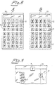
- the display device 7, in the form of stackable blocks according to Figure 2 can be built together, e.g. to form a keyboard 10, as illustrated in Figure 3.
- the keyboard 10 is thus made up from matrices that can form different sign blocks 7 and have a text window 11.
- the text window may have a plurality of sign displayers displaying the sign keyed-in with the aid of the respective block.
- Each block 7 may represent different signs, as will be apparent from Figures 3A and 3B. By touching block 12 "on", the remaining blocks 7 of the keyboard 10 can change sign character and function.
- a block 7 showing a "1" in Figure 3A (resulting in that on touch there is displayed a “1” in the window 11) can be switched to display an "A" after the block 12 has been touched, according to Figure 3B.
- this block functions as a key for keying in an "A" in the text window 11. Renewed touching of block 12 returns block 7 to the sign character and function illustrated in Figure 3A.
- the keyboard 10 illustrated in Figure 3 does not necessarily need to be made up from individual blocks 7, but can be formed as a single LCD unit. Accordingly, all "blocks 7, 12" and the different sign displayers of the text window 11 directly formed on the front cover window 1', as indicated by dashed lines in Figure 3. It will thus be understood that the dimensions of the keyboard 10 can be minimal. However there is nothing to stop the cover window 1' from being made large, since the key functions are not tied up with any elasticity or change in distance from the detection of AC, as is the case for touch controlled display devices in the prior art.
- control signals generated in the respective block/key 7, which are fed to the text window 11 in the illustrated embodiment may of course be utilised for treatment in a microprocessor or other form of data processor, or be stored in a memory.
- FIG 4 A further application for the inventive touch controlled display device is illustrated in Figure 4, namely as a switchboard in an industry such as a paper mill.
- the switchboard 13 may be formed with a single cover window 1' in an LCD unit.
- the display 13 may include stackable blocks 7, each of which has a different display character and switch function.
- Figure 4 merely illustrates a portion of a panel where the blocks 7 may be "illuminated” or “extinguished” or signal different operational functions for the machines the respective block is intended to affect.
- block “V” could relate to an openable and closable valve, block “p” to a connectable or disconnectable pump and the remaining blocks 7 to the regulation of the level of liquid in a tank.
- the fields of application are infinite for the touch controlled display device in accordance with the invention, due to the possibilities of variation in signs and symbols.
- the examples above refer to display devices with two displaying means 3, 4 (segments), but the invention is of course applicable to display devices with one or more segments, e.g. to ordinary number indicators with seven segments or sign matrices. Neither is the invention limited to LCD units, but is applicable to all display devices where individual displaying means are driven from one drive circuit. The present invention may therefore not be considered as limited to the embodiments described above and illustrated on the appended drawings.
Abstract
Description
- The present invention relates to a touch controlled display device including displaying means disposed on the inside of a front cover window of the device.
- Different such display devices are known. By touch control is here primarily intended a control where the operator touches the device with his finger.
- Accordingly, there are known such touch controlled display devices where control is exercised by the pressure action to which the device is subjected when the finger touches the device. Examples of pressure controlled display devices are mentioned in the Xerox Disclosure Journal, Vol. 5, No. 5, Sept./Oct., 1980, page 559, and in the German Offenlegungsschrift 30 39 713, as well as in the Japanese Published Specification 56-161521. In the latter there is utilized the capacity change occurring with pressure on the display device, by the distance being altered between detection electrodes and a counter-electrode, these electrodes being disposed on the inside of the respective front and back cover plates of the display device.
- These known pressure controlled display devices have troublesome disadvantages, since the cover plates must be elastic in order to be activated by the touch pressure and to return to their initial state after being touched. This elasticity is troublesome, particularly with display devices having a large surface, in which a touch easily results in that the electrodes come into direct contact with each other. Furthermore, repeated pressure loading results in risk of the cover plates becoming fatigued. Operational realiability in such known pressure controlled display devices has been found to be small.
- Another type of touch control is carried out with the aid of direct capacitative detection of the finger touch on the display device. In this case, separate touch contacts are placed on the outside of the cover plate or window of the display device. This type may be exemplified by the devices described in the British
Patent Applications 2 066 548 and 2 094 050 and the German Offenlegungsschrift 29 32 540. - All the touch control display devices known up to now have required separate detection or touch contacts, thus making the circuitry complicated due to the extra contacts requiring extra wiring. An advantage with disposing the detection contacts on the inside of the transparent window, e.g. in accordance with the cited Japanese publication, is that the problems of wear and dirtying which trouble all other known devices are dispensed with. However, apart from the mentioned disadvantages there is also a very serious problem with the known devices with separate detection contacts on the inside and outside of the window, namely that these separate contacts, in themselves and due to extra wiring, are extremely voluminous. The separate contacts must namely be disposed at a given distance from each other and from the customary displaying means in the display device. Wiring will be complicated, since the wires from the separate` contacts must be accommodated together with other feed and control wires for the customary displaying means.
- The disadvantage described above are entirely removed by the present invention. Characterizing for the invention is namely that at least one of the displaying means of the display device is adapted to form the capacitative sensing circuit, together with an electrode in the immediate vicinity of, but spaced from the same cover window. With the sensing circuit there is detected the capacitance change AC caused by the mere proximity of such as the operator's finger on the cover window outside. Accordingly, there is no pressure load or deformation of the cover window, and this may thus be in elastic. Neither is there any risk of the display member coming into direct contact with the counter-electrode.
- The problem with extra contacts that has so far obstructed miniaturization of activable display devices may be solved by two or more mutually close displaying means being included in the sensing circuit. The inventive subject thus results in extensive simplification of circuit structure, since the ordinary feed circuit wires of the display device may be utilized for the sensing circuit.
- The invention may be utilized for different forms of display device, e.g. those of the liquid crystal type (LCD). A natural application is for different kinds of switching means, from separate switch buttons to entire keyboards. Indications and changes on a display screen built up from LCD's, which have been performed by such as light pens when cathode ray tubes have been used, may now be performed to advantage with the operator's own finger.
- The inventive display device may further be self-indicating by it being able to show different statuses with the aid of different implementations of the displaying means,, e.g. by the means being presented in different colours. A further development of the invention is an LCD-type embodiment is also for an LCD drive unit and different types of output to be integrated in a complete switch.
- A simple switch formed in accordance with the present invention can to advantage replace both an LED and a mechanical switch. This means, inter alia, power savings and a switch that in principle can not be worn out. A very suitable embodiment includes an LCD means implemented as a matrix, possibly with a reversed cursor, the electronics then being able to reproduce different signs, numbers and letters simultaneously as the LCD means can give information to the rear, e.g. to a microprocessor. Switches of this kind can be stackable in both directions, and be manufactured according to the applicable mechanical standard dimensions. The invention may also be applied to known LCD means.
- Manufacture of the display device in accordance with the invention may be carried out in steps, and does not need to mean that a complete module be produced in one step. The following manufacturing steps may thus be applied:
- a) A double segment displaying means is manufactured and disposed in a switch housing.
- b) The product from step a) is supplemented by an LCD drive unit being built into the housing.
- c) Step b) is further developed by the displaying means being made with several outputs.
- d) Step c) is further developed, as is step d) in its turn etc., for providing different complete modules having functions described above.
- The invention will now be described below in more detail and with reference to the accompanying drawings relating to preferred embodiments, on which:
- Figure 1A illustrates the principle of a known LCD means with a sensing circuit for the detection of change in capacitance,
- Figure 1 B illustrates the principle of an LCD means in accordance with the present invention,
- Figure 2 illustrates a double segment displaying means with an integrated circuit executed in accordance with the invention,
- Figure 3 illustrates a keyboard with display devices in accordance with the invention, and
- Figure 4 is a section of a control panel with graphical symbols formed according to the present invention.
- Figure 1A illustrates the principle of a known touch controlled display device, e.g. of the type described in the Japanese Published Specification 56-161521. The device is formed as an LCD unit with a
front cover window 1 andback cover window 2. On the inside of thefront window 1 there arethin displaying means common counter-electrode 5 disposed on the inside of theback window 2 are intended to energise the liquid crystals (not shown) accommodated between thewindows means counter-electrode 5. This feed takes place via the pins 3', 4' and 5' respectively to each of themeans counter-electrode 5. - The known touch controlled LCD unit of Figure 1A has a
detection electrode 6, having a distance DH to thecounter-electrode 5 for an unenergised LCD unit. The detection electrode is connected to a pin 6' intended for connection to adetection circuit 9, which is also connected to the pin 5'. To energise the touch controlled LCD unit, an exterior force P must be applied, e.g. by an operator pressing a finger on thefront window 1 of the LCD unit. There thus occurs a change in distance of ADH, due to the elasticity of the window, the change ADH in turn giving rise to the capacitance C between thedetection electrode 6 andelectrode 5 being changed to a new value C' as long as the force P remains. The capacitance values C and C' are sensed by thedetection circuit 9 connected to the pins 5' and 6'. - As explained above, the known touch controlled display device is burdened with a series of problems making it unsuitable for use in different "utility articles". These problems are avoided with a touch controlled display device in accordance with the invention, the principle of which is illustrated in Figure 1B. The device illustrated in this Figure has, as with the known device of Figure 1A, front and
back cover windows front window 1 carries two display means 3,4, while the back window carries thecounter-electrode 5 on its inside. The device in accordance with the invention is driven in the same way as the known device by voltage feed via pins 3', 4' and 5' associated with themeans electrode 5. - In contradistinction to the principle for touch controlled display devices illustrated in Figure 1A, the inventive device does not need to have elastically deformable cover windows, and these are to advantage undeformable.
- Furthermore, there are no extra, separate electrodes and neither is there any extra wiring or connection pin for the
detection circuit 9. The normal displayingmeans front window 1, this capacitance value is changed by AC. This change AC can be sensed by thedetection circuit 9, which is connected to the pins 3', 4' similarly intended for driving the display device. - The capacitance change AC sensed by the
sensing circuit 9 causes an electrical signal which may be fed from thecircuit 9 to control apparatus of different kinds such as switches, microprocessors and the like. It should be noted that only one of the displaying means, e.g. that denoted by thenumeral 3, needs to be connected to the drive circuit, while the other (e.g. 4) is more or less to be regarded as a counter-electrode, which is accordingly never intended to illuminate. - In Figure 2 there is depicted a
display device 7 implemented such as to be stackable in accordance with the invention, and taking the form of an LCD unit with two displayingmeans device 7 is fed with voltage via connection pins 8, and includes an unillustrated integrated circuit. By touching thewindow 1, both displayingmeans 3, 4 (segments) on thefront cover window 1 can be caused to be switched for displaying a plus or a minus sign. - The
display device 7, in the form of stackable blocks according to Figure 2 can be built together, e.g. to form akeyboard 10, as illustrated in Figure 3. Thekeyboard 10 is thus made up from matrices that can formdifferent sign blocks 7 and have atext window 11. The text window may have a plurality of sign displayers displaying the sign keyed-in with the aid of the respective block. Eachblock 7 may represent different signs, as will be apparent from Figures 3A and 3B. By touchingblock 12 "on", the remainingblocks 7 of thekeyboard 10 can change sign character and function. For example, ablock 7 showing a "1" in Figure 3A (resulting in that on touch there is displayed a "1" in the window 11) can be switched to display an "A" after theblock 12 has been touched, according to Figure 3B. After such switching, this block functions as a key for keying in an "A" in thetext window 11. Renewed touching ofblock 12 returns block 7 to the sign character and function illustrated in Figure 3A. - The
keyboard 10 illustrated in Figure 3 does not necessarily need to be made up fromindividual blocks 7, but can be formed as a single LCD unit. Accordingly, all "blocks text window 11 directly formed on the front cover window 1', as indicated by dashed lines in Figure 3. It will thus be understood that the dimensions of thekeyboard 10 can be minimal. However there is nothing to stop the cover window 1' from being made large, since the key functions are not tied up with any elasticity or change in distance from the detection of AC, as is the case for touch controlled display devices in the prior art. - The control signals generated in the respective block/
key 7, which are fed to thetext window 11 in the illustrated embodiment, may of course be utilised for treatment in a microprocessor or other form of data processor, or be stored in a memory. - A further application for the inventive touch controlled display device is illustrated in Figure 4, namely as a switchboard in an industry such as a paper mill. As with the
keyboard 10 of Figure 3, theswitchboard 13 may be formed with a single cover window 1' in an LCD unit. Alternatively thedisplay 13 may includestackable blocks 7, each of which has a different display character and switch function. Figure 4 merely illustrates a portion of a panel where theblocks 7 may be "illuminated" or "extinguished" or signal different operational functions for the machines the respective block is intended to affect. For example, block "V" could relate to an openable and closable valve, block "p" to a connectable or disconnectable pump and the remainingblocks 7 to the regulation of the level of liquid in a tank. - As will be apparent from the exemplifications mentioned above, the fields of application are infinite for the touch controlled display device in accordance with the invention, due to the possibilities of variation in signs and symbols. The examples above refer to display devices with two displaying
means 3, 4 (segments), but the invention is of course applicable to display devices with one or more segments, e.g. to ordinary number indicators with seven segments or sign matrices. Neither is the invention limited to LCD units, but is applicable to all display devices where individual displaying means are driven from one drive circuit. The present invention may therefore not be considered as limited to the embodiments described above and illustrated on the appended drawings.
Claims (7)
Priority Applications (1)
| Application Number | Priority Date | Filing Date | Title |
|---|---|---|---|
| AT84900760T ATE47498T1 (en) | 1984-01-30 | 1984-01-30 | TOUCH CONTROLLED DISPLAY DEVICE. |
Applications Claiming Priority (1)
| Application Number | Priority Date | Filing Date | Title |
|---|---|---|---|
| PCT/SE1984/000028 WO1985003374A1 (en) | 1984-01-30 | 1984-01-30 | Touch controlled display device |
Publications (2)
| Publication Number | Publication Date |
|---|---|
| EP0203914A1 EP0203914A1 (en) | 1986-12-10 |
| EP0203914B1 true EP0203914B1 (en) | 1989-10-18 |
Family
ID=20354210
Family Applications (1)
| Application Number | Title | Priority Date | Filing Date |
|---|---|---|---|
| EP84900760A Expired EP0203914B1 (en) | 1984-01-30 | 1984-01-30 | Touch controlled display device |
Country Status (7)
| Country | Link |
|---|---|
| US (1) | US4910504A (en) |
| EP (1) | EP0203914B1 (en) |
| JP (1) | JPS62502634A (en) |
| AT (1) | ATE47498T1 (en) |
| DE (2) | DE3480237D1 (en) |
| GB (1) | GB2179160B (en) |
| WO (1) | WO1985003374A1 (en) |
Cited By (1)
| Publication number | Priority date | Publication date | Assignee | Title |
|---|---|---|---|---|
| CN102239462A (en) * | 2008-12-05 | 2011-11-09 | 苹果公司 | Integrated touch panel for a tft display |
Families Citing this family (42)
| Publication number | Priority date | Publication date | Assignee | Title |
|---|---|---|---|---|
| JPS6177920A (en) * | 1984-09-22 | 1986-04-21 | Sharp Corp | Device for input and liquid crystal display |
| US5450069A (en) * | 1987-09-04 | 1995-09-12 | Copytele, Inc. | Data/facsimile telephone subset apparatus incorporating electrophoretic displays |
| FR2632793B1 (en) * | 1988-06-08 | 1994-04-15 | Jaeger | IMPROVED BUTTON EXPLOITING THE PROPERTIES OF A LIQUID CRYSTAL |
| US5225959A (en) * | 1991-10-15 | 1993-07-06 | Xerox Corporation | Capacitive tactile sensor array and method for sensing pressure with the array |
| JP3050348B2 (en) * | 1992-04-17 | 2000-06-12 | インターナショナル・ビジネス・マシーンズ・コーポレイション | Method and apparatus for user control in a process control system |
| US5381388A (en) * | 1993-07-28 | 1995-01-10 | Technomarket, L.P. | Digital clock |
| US5483235A (en) * | 1994-02-23 | 1996-01-09 | At&T Corp. | Stylus-based keyboard key arrangement |
| US6476798B1 (en) * | 1994-08-22 | 2002-11-05 | International Game Technology | Reduced noise touch screen apparatus and method |
| GB9422911D0 (en) * | 1994-11-14 | 1995-01-04 | Moonstone Technology Ltd | Capacitive touch detectors |
| US5801340A (en) * | 1995-06-29 | 1998-09-01 | Invotronics Manufacturing | Proximity sensor |
| US6061050A (en) * | 1995-10-27 | 2000-05-09 | Hewlett-Packard Company | User interface device |
| US5796183A (en) * | 1996-01-31 | 1998-08-18 | Nartron Corporation | Capacitive responsive electronic switching circuit |
| US7663607B2 (en) | 2004-05-06 | 2010-02-16 | Apple Inc. | Multipoint touchscreen |
| CN1203627C (en) | 2000-07-26 | 2005-05-25 | 皇家菲利浦电子有限公司 | Radio communication system |
| TWI245252B (en) * | 2002-07-18 | 2005-12-11 | Gigno Technology Co Ltd | LCD and the touch-control method thereof |
| JP2005005058A (en) * | 2003-06-10 | 2005-01-06 | Omron Corp | Conductor detection switch |
| US8531431B2 (en) | 2003-10-13 | 2013-09-10 | Integritouch Development Ab | High speed 3D multi touch sensitive device |
| SE525614C2 (en) * | 2003-10-13 | 2005-03-22 | Anders Swedin | Touch sensitive display device e.g. LCD for mobile telephone, has switch that connect interface and measuring circuit to display electrode on front or back substrates, in different states of operation, respectively |
| US20050116020A1 (en) * | 2003-11-07 | 2005-06-02 | Smolucha Walter E. | Locating individuals and games in a gaming establishment |
| US20050122119A1 (en) * | 2003-12-05 | 2005-06-09 | Touchram Llc | Low noise proximity sensing system |
| GB2411278B (en) * | 2004-02-20 | 2008-05-07 | Pelikon Ltd | Improved displays |
| US20050233287A1 (en) * | 2004-04-14 | 2005-10-20 | Vladimir Bulatov | Accessible computer system |
| US20060287078A1 (en) * | 2004-04-22 | 2006-12-21 | Smolucha Walter E | Identifying components of a casino game |
| US8776049B2 (en) * | 2004-10-20 | 2014-07-08 | Seagate Technology Llc | Address aligned resource set allocation in a memory space |
| DE102004060846B4 (en) * | 2004-12-17 | 2008-12-18 | Diehl Ako Stiftung & Co. Kg | Capacitive touch switch |
| US7330108B2 (en) * | 2005-02-24 | 2008-02-12 | Wms Gaming Inc. | Security zones for casino gaming |
| US20060258442A1 (en) * | 2005-05-13 | 2006-11-16 | Ryan Chad A | Multi-purpose casino chips |
| US7609178B2 (en) * | 2006-04-20 | 2009-10-27 | Pressure Profile Systems, Inc. | Reconfigurable tactile sensor input device |
| JP2009509194A (en) | 2005-09-20 | 2009-03-05 | ケンライト,デビッド,ノリス | Proximity-responsive display material apparatus and method |
| KR101759853B1 (en) * | 2006-06-09 | 2017-07-19 | 애플 인크. | Touch screen liquid crystal display |
| US8259078B2 (en) * | 2006-06-09 | 2012-09-04 | Apple Inc. | Touch screen liquid crystal display |
| CN104965621B (en) * | 2006-06-09 | 2018-06-12 | 苹果公司 | Touch screen LCD and its operating method |
| US8493330B2 (en) | 2007-01-03 | 2013-07-23 | Apple Inc. | Individual channel phase delay scheme |
| US9710095B2 (en) * | 2007-01-05 | 2017-07-18 | Apple Inc. | Touch screen stack-ups |
| US8040326B2 (en) | 2007-06-13 | 2011-10-18 | Apple Inc. | Integrated in-plane switching display and touch sensor |
| US8144295B2 (en) | 2008-11-18 | 2012-03-27 | Apple Inc. | Common bus design for a TFT-LCD display |
| US8804056B2 (en) | 2010-12-22 | 2014-08-12 | Apple Inc. | Integrated touch screens |
| US9395583B2 (en) | 2012-06-06 | 2016-07-19 | Apple Inc. | Column spacer design for a display incorporating a third metal layer |
| US10268295B2 (en) | 2014-04-16 | 2019-04-23 | Apple Inc. | Structure for pixelated self-capacitance |
| US9367188B2 (en) | 2014-05-23 | 2016-06-14 | Apple Inc. | RC matching in a touch screen |
| US10852876B2 (en) | 2014-05-28 | 2020-12-01 | Apple Inc. | Narrow border touch screen |
| CN104932822B (en) * | 2015-06-03 | 2018-10-23 | 昆山国显光电有限公司 | Human-computer interaction device and method, input equipment and output equipment for manufacturing it |
Family Cites Families (11)
| Publication number | Priority date | Publication date | Assignee | Title |
|---|---|---|---|---|
| NL184138C (en) * | 1977-07-30 | 1989-04-17 | Ti Corporate Services | TIP KEY SWITCH. |
| US4224615A (en) * | 1978-09-14 | 1980-09-23 | Texas Instruments Incorporated | Method of using a liquid crystal display device as a data input device |
| DE2932540A1 (en) * | 1979-08-09 | 1981-02-26 | Deutsche Telephonwerk Kabel | Keyboard sensor field with touch contacts - consists of conducting foil or plate arranged over liq. crystal display |
| US4290061A (en) * | 1979-08-23 | 1981-09-15 | General Electric Company | Electrically integrated touch input and output display system |
| JPS5678893A (en) * | 1979-11-30 | 1981-06-29 | Casio Computer Co Ltd | Input device for electronic musical instrument |
| JPS56161521A (en) * | 1980-05-16 | 1981-12-11 | Canon Inc | Liquid crystal display device |
| DE3039713A1 (en) * | 1980-10-21 | 1982-05-27 | Siemens Ag | Inter active liquid crystal display - records required points upon short-circuit between opposing electrodes in response to applied pressure |
| JPS5795032A (en) * | 1980-12-03 | 1982-06-12 | Casio Computer Co Ltd | Touch switching device |
| US4639720A (en) * | 1981-01-12 | 1987-01-27 | Harris Corporation | Electronic sketch pad |
| GB2094050A (en) * | 1981-02-28 | 1982-09-08 | Racal Res Ltd | Improvements in and relating to display systems |
| EP0079711A3 (en) * | 1981-11-16 | 1984-10-03 | The Secretary of State for Defence in Her Britannic Majesty's Government of the United Kingdom of Great Britain and | Touch sensitive switches |
-
1984
- 1984-01-30 US US07/143,202 patent/US4910504A/en not_active Expired - Lifetime
- 1984-01-30 AT AT84900760T patent/ATE47498T1/en active
- 1984-01-30 GB GB08617438A patent/GB2179160B/en not_active Expired
- 1984-01-30 WO PCT/SE1984/000028 patent/WO1985003374A1/en active IP Right Grant
- 1984-01-30 DE DE8484900760T patent/DE3480237D1/en not_active Expired
- 1984-01-30 JP JP59500866A patent/JPS62502634A/en not_active Withdrawn
- 1984-01-30 DE DE19843490635 patent/DE3490635T1/de not_active Withdrawn
- 1984-01-30 EP EP84900760A patent/EP0203914B1/en not_active Expired
Cited By (2)
| Publication number | Priority date | Publication date | Assignee | Title |
|---|---|---|---|---|
| CN102239462A (en) * | 2008-12-05 | 2011-11-09 | 苹果公司 | Integrated touch panel for a tft display |
| CN102239462B (en) * | 2008-12-05 | 2014-11-05 | 苹果公司 | Integrated touch panel for a TFT display |
Also Published As
| Publication number | Publication date |
|---|---|
| EP0203914A1 (en) | 1986-12-10 |
| DE3480237D1 (en) | 1989-11-23 |
| US4910504A (en) | 1990-03-20 |
| WO1985003374A1 (en) | 1985-08-01 |
| JPS62502634A (en) | 1987-10-08 |
| GB8617438D0 (en) | 1986-08-28 |
| GB2179160B (en) | 1988-11-09 |
| GB2179160A (en) | 1987-02-25 |
| ATE47498T1 (en) | 1989-11-15 |
| DE3490635T1 (en) | 1987-03-12 |
Similar Documents
| Publication | Publication Date | Title |
|---|---|---|
| EP0203914B1 (en) | Touch controlled display device | |
| US4224615A (en) | Method of using a liquid crystal display device as a data input device | |
| US4405921A (en) | Liquid crystal display device | |
| US4334219A (en) | Operation setting device having stationary touch-sensitive control elements | |
| US4893115A (en) | Touch sensitive visual display system | |
| EP0053061B1 (en) | Hand-held computer | |
| US6028591A (en) | Keyboard with flexible display and prompt capability | |
| US4363029A (en) | Switch for sensing proximity of an operator | |
| US20050179668A1 (en) | Electronic device with a flat panel display and touch buttons/pads outside the display area | |
| CN105278782A (en) | Display device provided with sensor and method of driving the same | |
| GB1461978A (en) | Electronic business telephone | |
| EP0232137A2 (en) | Improvements in or relating to relegendable pushbutton switches | |
| US20150234525A1 (en) | Powered card with touch display | |
| US4380371A (en) | Liquid crystal display device | |
| GB2154356A (en) | Liquid crystal display panel | |
| JPS5871519A (en) | Illumination switch | |
| US4256376A (en) | Electro-optical display element | |
| US20230063378A1 (en) | Keyboard apparatus with changeable key displays | |
| CN212380071U (en) | Integrated nixie tube and electronic equipment | |
| JP3162454B2 (en) | Display control device | |
| JPS62245359A (en) | Electronic calculator | |
| JPH0112350Y2 (en) | ||
| JPS6272023A (en) | Keyboard device | |
| JPS6184724A (en) | Input output device | |
| JPS6022385Y2 (en) | Display device with input section |
Legal Events
| Date | Code | Title | Description |
|---|---|---|---|
| PUAI | Public reference made under article 153(3) epc to a published international application that has entered the european phase |
Free format text: ORIGINAL CODE: 0009012 |
|
| 17P | Request for examination filed |
Effective date: 19860725 |
|
| AK | Designated contracting states |
Kind code of ref document: A1 Designated state(s): AT BE CH DE FR GB LI LU NL SE |
|
| 17Q | First examination report despatched |
Effective date: 19881219 |
|
| GRAA | (expected) grant |
Free format text: ORIGINAL CODE: 0009210 |
|
| AK | Designated contracting states |
Kind code of ref document: B1 Designated state(s): AT BE CH DE FR GB LI LU NL SE |
|
| PG25 | Lapsed in a contracting state [announced via postgrant information from national office to epo] |
Ref country code: BE Effective date: 19891018 Ref country code: AT Effective date: 19891018 |
|
| REF | Corresponds to: |
Ref document number: 47498 Country of ref document: AT Date of ref document: 19891115 Kind code of ref document: T |
|
| REF | Corresponds to: |
Ref document number: 3480237 Country of ref document: DE Date of ref document: 19891123 |
|
| PG25 | Lapsed in a contracting state [announced via postgrant information from national office to epo] |
Ref country code: GB Effective date: 19900129 |
|
| PG25 | Lapsed in a contracting state [announced via postgrant information from national office to epo] |
Ref country code: LU Free format text: LAPSE BECAUSE OF NON-PAYMENT OF DUE FEES Effective date: 19900131 |
|
| ET | Fr: translation filed | ||
| PLBE | No opposition filed within time limit |
Free format text: ORIGINAL CODE: 0009261 |
|
| STAA | Information on the status of an ep patent application or granted ep patent |
Free format text: STATUS: NO OPPOSITION FILED WITHIN TIME LIMIT |
|
| 26N | No opposition filed | ||
| GBPC | Gb: european patent ceased through non-payment of renewal fee | ||
| EAL | Se: european patent in force in sweden |
Ref document number: 84900760.4 |
|
| PGFP | Annual fee paid to national office [announced via postgrant information from national office to epo] |
Ref country code: NL Payment date: 19990131 Year of fee payment: 16 |
|
| PGFP | Annual fee paid to national office [announced via postgrant information from national office to epo] |
Ref country code: CH Payment date: 19990211 Year of fee payment: 16 |
|
| PG25 | Lapsed in a contracting state [announced via postgrant information from national office to epo] |
Ref country code: LI Free format text: LAPSE BECAUSE OF NON-PAYMENT OF DUE FEES Effective date: 20000131 Ref country code: CH Free format text: LAPSE BECAUSE OF NON-PAYMENT OF DUE FEES Effective date: 20000131 |
|
| PG25 | Lapsed in a contracting state [announced via postgrant information from national office to epo] |
Ref country code: NL Free format text: LAPSE BECAUSE OF NON-PAYMENT OF DUE FEES Effective date: 20000801 |
|
| REG | Reference to a national code |
Ref country code: CH Ref legal event code: PL |
|
| NLV4 | Nl: lapsed or anulled due to non-payment of the annual fee |
Effective date: 20000801 |
|
| REG | Reference to a national code |
Ref country code: FR Ref legal event code: TP |
|
| PGFP | Annual fee paid to national office [announced via postgrant information from national office to epo] |
Ref country code: SE Payment date: 20020524 Year of fee payment: 19 |
|
| PGFP | Annual fee paid to national office [announced via postgrant information from national office to epo] |
Ref country code: FR Payment date: 20020530 Year of fee payment: 19 |
|
| PGFP | Annual fee paid to national office [announced via postgrant information from national office to epo] |
Ref country code: DE Payment date: 20020628 Year of fee payment: 19 |
|
| PG25 | Lapsed in a contracting state [announced via postgrant information from national office to epo] |
Ref country code: SE Free format text: LAPSE BECAUSE OF NON-PAYMENT OF DUE FEES Effective date: 20030131 |
|
| PG25 | Lapsed in a contracting state [announced via postgrant information from national office to epo] |
Ref country code: DE Free format text: LAPSE BECAUSE OF NON-PAYMENT OF DUE FEES Effective date: 20030801 |
|
| EUG | Se: european patent has lapsed | ||
| PG25 | Lapsed in a contracting state [announced via postgrant information from national office to epo] |
Ref country code: FR Free format text: LAPSE BECAUSE OF NON-PAYMENT OF DUE FEES Effective date: 20030930 |
|
| REG | Reference to a national code |
Ref country code: FR Ref legal event code: ST |