EP0210618A2 - Frequency converter for use in a laser printer - Google Patents
Frequency converter for use in a laser printer Download PDFInfo
- Publication number
- EP0210618A2 EP0210618A2 EP86110354A EP86110354A EP0210618A2 EP 0210618 A2 EP0210618 A2 EP 0210618A2 EP 86110354 A EP86110354 A EP 86110354A EP 86110354 A EP86110354 A EP 86110354A EP 0210618 A2 EP0210618 A2 EP 0210618A2
- Authority
- EP
- European Patent Office
- Prior art keywords
- frequency
- signal
- modulator
- speed
- laser printer
- Prior art date
- Legal status (The legal status is an assumption and is not a legal conclusion. Google has not performed a legal analysis and makes no representation as to the accuracy of the status listed.)
- Granted
Links
Images

Classifications
-
- H—ELECTRICITY
- H04—ELECTRIC COMMUNICATION TECHNIQUE
- H04N—PICTORIAL COMMUNICATION, e.g. TELEVISION
- H04N1/00—Scanning, transmission or reproduction of documents or the like, e.g. facsimile transmission; Details thereof
- H04N1/04—Scanning arrangements, i.e. arrangements for the displacement of active reading or reproducing elements relative to the original or reproducing medium, or vice versa
- H04N1/047—Detection, control or error compensation of scanning velocity or position
- H04N1/053—Detection, control or error compensation of scanning velocity or position in main scanning direction, e.g. synchronisation of line start or picture elements in a line
-
- G—PHYSICS
- G06—COMPUTING; CALCULATING OR COUNTING
- G06K—GRAPHICAL DATA READING; PRESENTATION OF DATA; RECORD CARRIERS; HANDLING RECORD CARRIERS
- G06K15/00—Arrangements for producing a permanent visual presentation of the output data, e.g. computer output printers
- G06K15/02—Arrangements for producing a permanent visual presentation of the output data, e.g. computer output printers using printers
- G06K15/12—Arrangements for producing a permanent visual presentation of the output data, e.g. computer output printers using printers by photographic printing, e.g. by laser printers
- G06K15/1204—Arrangements for producing a permanent visual presentation of the output data, e.g. computer output printers using printers by photographic printing, e.g. by laser printers involving the fast moving of an optical beam in the main scanning direction
- G06K15/1219—Detection, control or error compensation of scanning velocity or position, e.g. synchronisation
-
- H—ELECTRICITY
- H04—ELECTRIC COMMUNICATION TECHNIQUE
- H04N—PICTORIAL COMMUNICATION, e.g. TELEVISION
- H04N1/00—Scanning, transmission or reproduction of documents or the like, e.g. facsimile transmission; Details thereof
- H04N1/04—Scanning arrangements, i.e. arrangements for the displacement of active reading or reproducing elements relative to the original or reproducing medium, or vice versa
- H04N1/113—Scanning arrangements, i.e. arrangements for the displacement of active reading or reproducing elements relative to the original or reproducing medium, or vice versa using oscillating or rotating mirrors
- H04N1/1135—Scanning arrangements, i.e. arrangements for the displacement of active reading or reproducing elements relative to the original or reproducing medium, or vice versa using oscillating or rotating mirrors for the main-scan only
-
- H—ELECTRICITY
- H04—ELECTRIC COMMUNICATION TECHNIQUE
- H04N—PICTORIAL COMMUNICATION, e.g. TELEVISION
- H04N2201/00—Indexing scheme relating to scanning, transmission or reproduction of documents or the like, and to details thereof
- H04N2201/024—Indexing scheme relating to scanning, transmission or reproduction of documents or the like, and to details thereof deleted
- H04N2201/02406—Arrangements for positioning elements within a head
- H04N2201/02439—Positioning method
- H04N2201/02443—Positioning method using adhesive
-
- H—ELECTRICITY
- H04—ELECTRIC COMMUNICATION TECHNIQUE
- H04N—PICTORIAL COMMUNICATION, e.g. TELEVISION
- H04N2201/00—Indexing scheme relating to scanning, transmission or reproduction of documents or the like, and to details thereof
- H04N2201/04—Scanning arrangements
- H04N2201/047—Detection, control or error compensation of scanning velocity or position
- H04N2201/04753—Control or error compensation of scanning position or velocity
- H04N2201/04758—Control or error compensation of scanning position or velocity by controlling the position of the scanned image area
- H04N2201/04767—Control or error compensation of scanning position or velocity by controlling the position of the scanned image area by controlling the timing of the signals, e.g. by controlling the frequency o phase of the pixel clock
- H04N2201/04768—Controlling the frequency of the signals
- H04N2201/04774—Controlling the frequency of the signals using a reference clock or oscillator
-
- H—ELECTRICITY
- H04—ELECTRIC COMMUNICATION TECHNIQUE
- H04N—PICTORIAL COMMUNICATION, e.g. TELEVISION
- H04N2201/00—Indexing scheme relating to scanning, transmission or reproduction of documents or the like, and to details thereof
- H04N2201/04—Scanning arrangements
- H04N2201/047—Detection, control or error compensation of scanning velocity or position
- H04N2201/04753—Control or error compensation of scanning position or velocity
- H04N2201/04794—Varying the control or compensation during the scan, e.g. using continuous feedback or from line to line
- H04N2201/04798—Varying the main-scan control during the main-scan, e.g. facet tracking
Definitions
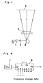
- the present invention relates to a device for use in a laser printer using a polygon mirror for light spot scanning on a photosensitive member and more particularly to a frequency converter for use in changing clock frequency for controlling print data speed corresponding to the change of the light spot speed due to change of the light projection angle of the polygon mirror.
- a laser diode 1 is intermittently driven to emit pulsive laser light lays corresponding to the printing data and the pulsive laser light lays are focused onto a cylindrical photosensitive member 3 through a collimating lens 2.
- a rotating polygon mirror 4 and f- 8 lens are disposed between the collimating lens 2 and the photosensitive member 3.
- the polygon mirror 4 causes the laser light beam to scan on the photosensitive member 3 in a rapid speed.
- the laser diode 1 is turned on and off corresponding to the rotation of a motor (not shown) which rotates the polygon mirror 4 so that desired parts of the surface of the photosensitive member 3 can be exposed by the laser light beam.
- the f- e lens 5 is provided by the following reason mentioned below.
- the rotation speed of the polygon mirror is kept constant by the motor (not shown)
- the light spot speed of the laser light on the photosensitive member 3 is faster as away from the center towards the both side ends than the speed at the center of the photosensitive member 3, whereby the dot pitch becomes large on both sides in case the printing data is applied at a constant speed.
- a rotation plane mirror 6 is used in place of using the polygon mirror 4. It is noted that the error due to the replacement is few.
- 8 wt, w; angular speed of the plane mirror 6. Accordingly the light spot speed v on the photosensitive member 3 is
- the f- 6 lens 5 is disposed between the rotation polygon mirror 4 and the photosensitive member 3.
- the f- 8 lens 5 has such a characteristic that the light beam tend to be displaced inwardly as the light goes to the periphery of the mirror 4 so that the light beam from the laser diode 1 is focused on the photosensitive member 3 and the scanning distance is proportional to the scanning time.
- the f- 8 lens must have a specialized structure and much expensive which causes the cost of the laser printer to be expensive.
- One approach is to correct the f- ⁇ distortion by changing the clock frequency of the pulses used for controlling the speed of the printing data corresponding to the light spot speed as shown in Fig. 3.
- a clock pulse oscillator 7 and a frequency divider 8 are used so that the frequency of the clock pulse of the oscillator 7 is divided and changed in the frequency divider 8 1 % by 1 %.
- the frequency divider 8 consists of seven stage flip flops so as to obtain eight kinds of frequency dividing ratios of 1/128 to 1/121 in response to the frequency change data signal applied to the terminals A, B and C, thereby to produce the printing data clock pulse having desired clock frequencies from the terminal QG.
- the conventional laser printer as the printing clock pulse of about 10MHz is used, so that the pulse frequency of the oscillator 7 must be 1.28GHz.
- the f- 6 correction arrangement mentioned above is not available for the practical use.
- An essential object of the present invention is to provide a frequency control device for use in a laser printer which can be fabricated by logic devices which are commercially available and acting the almost same operation of the f- 8 correction device as mentioned above.
- a frequency control device for use in a laser printer for controlling the printing data speed of the laser printer which comprises an oscillator for generating pulses of a predetermined frequency, a frequency control device which comprises a variable frequency divider for dividing frequency of the pulses generated from the oscillator by a desired frequency dividing ratio, a modulator for modulating the output of said oscillator by the output signal from the variable frequency divider so as to provide a modulated signal and a band pass filter for deriving a part of frequency component of the modulated signal of the modulator for generating a clock signal for controlling the printing data, said clock signal having frequency of controlling the speed of the printing data.
- the variable frequency divider divides the output frequency of the pulse of the oscillator with a relatively high change rate of the frequency.
- the modulator modulates the output pulses of the oscillator by the modulation signal which is the output of the variable frequency divider. Since the output signals thus modulated in the modulator has various kinds of frequency components, the band pass filter derives the pulse signal having the desired frequency component for controlling the speed of the printing data for compensating the scanning speed of the laser light spot of the printing data. Even though the output frequency of the variable frequency, divider changes with relatively high rate, the frequency of the output.of the band pass filter changes with a relatively low rate to obtain the desired frequency suitable to control the light spot speed of the laser printer.
- the f- ⁇ correetion can be made using commercially available logic devices without using expensive f- ⁇ lens, it becomes possible to reduce the cost of the laser printer.
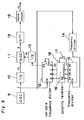
- an oscillator 9 generates an original pulse train of a frequency f to a 1/2 frequency divider 10 composed of flip-flops (not shown) in which each output pulse of the oscillator 9 is shaped into a rectangular shape pulse with 50% of on-off duty.
- the output pulses of the frequency divider 10 are fed to a modulation circuit 11 as a signal fc to be modulated.
- the output pulses of the oscillator 9 are fed to a variable frequency divider 12 in which the frequency of the original pulses is divided by a predetermined frequency ratio indicated by a frequency change signal mentioned later.
- the output pulses of the variable frequency divider 12 are further converted into a rectangular shape pulses with 50% duty in a second 1/2 frequency divider 13 and the converted pulses are fed to a modulation circuit 11 as a modulation signal f ⁇ .
- the signal fc to be modulated fed from the first 1/2 frequency divider 10 is modulated by the modulation signal f A fed from the second 1/2 frequency divider 13.
- the clock frequency for deciding the print data speed (referred to as print speed clock frequency hereinafter) coincides accurately with the bright point speed rate as shown in Fig. 3 but it may be sufficient to make the clock frequency nearly equal the bright point speed rate stepwisely.
- a third frequency divider 14 the frequency dividing ratio is set to divide the scanning period of the printing area equally sixteenth as shown in Fig. 7.
- a fourth frequency divider 15 counts the 16 time blocks using the output of the third frequency divider 14 and produces the output of the result of the count in a form of 16 system number.
- a polarity reversing circuit 16 is composed of a plurality of exclusive OR gates 16' so that the circuit 16 acts as the inverters connected to the three channels Q A , Q B and Q C when the output Q D of the fourth frequency divider 15, which is applied to the polarity reversing circuit 16 is low level and as the buffers connected to the three channels when the output Q D is high level, thereby resulting in reversing the polarity with respect to the center S of the photosensitive member 3.
- the modulation circuit 11 an amplitude modulation circuit is used.
- the output signal S of the modulation circuit 11 can be expressed as The output of the modulation circuit 11 has such frequency distribution as shown in Fig. 7.
- the frequency fc + f A can be derived from the frequency components by a band pass filter 18.
- a balanced modulator may be used as the modulation circuit 11.
- the output signal S is expressed by The output of the balanced modulator has such frequency distribution as shown in Fig. 9. In this case, since the component fc is absent, design of the band pass filter 11 may be easier.
- the frequency distribution near the modulation signal fc becomes such frequency distribution as shown in Fig. 9 and no problem occurs in the actual use.
- a desired signal may have a slight displacement of the frequency component near the frequency of f c + f ⁇ due to the operation of the variable frequency divider 10.
- the desired signal can be obtained by the band pass filter 18 so far as the band pass filter 18 has the frequency characteristic Bp shown in the dotted line in Fig. 10
- the ideal characteristic of the band pass filter 18 is such that only the frequency fc + f Acan be derived but the frequency component higher than fc + 3f Aand frequency component lower than fc - f Aare excluded.
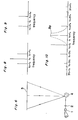
- the output signal of sine wave of the band pass filter 18 is converted into a pulse signal by the wave shaping circuit 19 so as to produce the clock frequency signal f0 for printing as shown in Fig. 7.
- the ratio frequency f0 in Fig. 7 shows the ratio of the frequencies at various position on the photosensitive member 3 with the frequency of the center of the photosensitive member 8 defined 1 and as shown in the lower half portion of Fig. 7, the ratio frequency is expressed in the stepped manner approximating to the light spot speed ratio shown in Fig. 3. It is noted that in Fig. 7, 015 and 016 represent the outputs of the dividers 15 and 16 and f12 represents the frequency dividing ratio of the divider 12.
- the printing speed As the printing speed is controlled by the clock frequency signal, the printing speed can be changed corresponding to the light spot speed, whereby the dot pitch becomes uniform independent of the position of the photosensitive member even if the f- ⁇ lens 6 is omitted as shown in Fig. 6.
- Fig. 6 like parts similar to Fig. 1 are represented by like reference numerals.
Abstract
Description
- The present invention relates to a device for use in a laser printer using a polygon mirror for light spot scanning on a photosensitive member and more particularly to a frequency converter for use in changing clock frequency for controlling print data speed corresponding to the change of the light spot speed due to change of the light projection angle of the polygon mirror.
- In the laser printer, as shown in Fig. 1, a
laser diode 1 is intermittently driven to emit pulsive laser light lays corresponding to the printing data and the pulsive laser light lays are focused onto a cylindricalphotosensitive member 3 through a collimatinglens 2. A rotatingpolygon mirror 4 and f- 8 lens are disposed between the collimatinglens 2 and thephotosensitive member 3. Thepolygon mirror 4 causes the laser light beam to scan on thephotosensitive member 3 in a rapid speed. Thelaser diode 1 is turned on and off corresponding to the rotation of a motor (not shown) which rotates thepolygon mirror 4 so that desired parts of the surface of thephotosensitive member 3 can be exposed by the laser light beam. - f-
e lens 5 is provided by the following reason mentioned below. As the rotation speed of the polygon mirror is kept constant by the motor (not shown), the light spot speed of the laser light on thephotosensitive member 3 is faster as away from the center towards the both side ends than the speed at the center of thephotosensitive member 3, whereby the dot pitch becomes large on both sides in case the printing data is applied at a constant speed. In order to make the calculation, it is assumed that arotation plane mirror 6 is used in place of using thepolygon mirror 4. It is noted that the error due to the replacement is few. Assuming that the angle between the optical axis of thelaser diode 1 and theplane mirror 6 is θ+ 45°, the distance x from the center S of thephotosensitive member 3 to the spot position P is x =ℓtan 2 θ. Wherein 8= wt, w; angular speed of theplane mirror 6. Accordingly the light spot speed v on thephotosensitive member 3 is - v(t) = dx/dt = 2w ℓsec2 (2wt).
- The light spot speed rate is
- [v(t)/vt=0] = sec2 (2wt).
- The relation between the spot position and the light spot speed rate can be depicted in Fig. 3.
- In order to correct the distortion of f (focus distance) - θ (incident angle), the f- 6
lens 5 is disposed between therotation polygon mirror 4 and thephotosensitive member 3. The f- 8lens 5 has such a characteristic that the light beam tend to be displaced inwardly as the light goes to the periphery of themirror 4 so that the light beam from thelaser diode 1 is focused on thephotosensitive member 3 and the scanning distance is proportional to the scanning time. - The f- 8 lens must have a specialized structure and much expensive which causes the cost of the laser printer to be expensive.
- Therefore, it is strongly desired to provide an inexpensive f- 6 correcting device.
- One approach is to correct the f- θ distortion by changing the clock frequency of the pulses used for controlling the speed of the printing data corresponding to the light spot speed as shown in Fig. 3.
- One known example device for the above purpose is shown in Fig. 4, wherein a
clock pulse oscillator 7 and afrequency divider 8 are used so that the frequency of the clock pulse of theoscillator 7 is divided and changed in thefrequency divider 8 1 % by 1 %. Thefrequency divider 8 consists of seven stage flip flops so as to obtain eight kinds of frequency dividing ratios of 1/128 to 1/121 in response to the frequency change data signal applied to the terminals A, B and C, thereby to produce the printing data clock pulse having desired clock frequencies from the terminal QG. However, in the conventional laser printer, as the printing clock pulse of about 10MHz is used, so that the pulse frequency of theoscillator 7 must be 1.28GHz. However such high speed logic devices are not commercially available and therefore, the f- 6 correction arrangement mentioned above is not available for the practical use. - An essential object of the present invention is to provide a frequency control device for use in a laser printer which can be fabricated by logic devices which are commercially available and acting the almost same operation of the f- 8 correction device as mentioned above.
- In order to accomplish the object of the present invention mentioned above, there is provided a frequency control device for use in a laser printer for controlling the printing data speed of the laser printer which comprises an oscillator for generating pulses of a predetermined frequency, a frequency control device which comprises a variable frequency divider for dividing frequency of the pulses generated from the oscillator by a desired frequency dividing ratio, a modulator for modulating the output of said oscillator by the output signal from the variable frequency divider so as to provide a modulated signal and a band pass filter for deriving a part of frequency component of the modulated signal of the modulator for generating a clock signal for controlling the printing data, said clock signal having frequency of controlling the speed of the printing data.
- In the arrangement mentioned above, the variable frequency divider divides the output frequency of the pulse of the oscillator with a relatively high change rate of the frequency. The modulator modulates the output pulses of the oscillator by the modulation signal which is the output of the variable frequency divider. Since the output signals thus modulated in the modulator has various kinds of frequency components, the band pass filter derives the pulse signal having the desired frequency component for controlling the speed of the printing data for compensating the scanning speed of the laser light spot of the printing data. Even though the output frequency of the variable frequency, divider changes with relatively high rate, the frequency of the output.of the band pass filter changes with a relatively low rate to obtain the desired frequency suitable to control the light spot speed of the laser printer.
- According to the present invention, since the f-θcorreetion can be made using commercially available logic devices without using expensive f- θlens, it becomes possible to reduce the cost of the laser printer.
-
- Fig. 1 is a schematic diagram showing general arrangement of a laser printer in which a polygonal mirror is used for scanning laser light
- Fig. 2 is a schematic diagram showing a general arrangement of a laser printer in which a plane mirror is used for scanning the laser light,
- Fig. 3 is a schematic diagram showing the variation of the light spot speed with respect to the scanning position of the laser light,
- Fig. 4 is a block diagram of an example of a proposed frequency control circuit,
- Fig. 5 is a block diagram of an example of a frequency control circuit according to the present invention,
- Fig. 6 is a schematic diagram showing an arrangement of the optical system used in the laser printer in which the frequency control device according to the present invention is used,
- Fig. 7 is a schematic diagram showing operation of the circuit arrangement of Fig. 1 with the change of the frequency depicted,
- Fig. 8 is a schematic diagram showing the frequency spectrum of the output signal of the frequency control device shown in Fig. 5 in which an AM modulator is used,
- Fig. 9 is a schematic diagram showing the frequency spectrum of the output signal of the frequency control device shown in Fig. 5 in which a balanced modulator is used,
- Fig. 10 is a schematic diagram showing the frequency spectrum of the output signal of the frequency control device shown in Fig. 5 in which the modulator is composed of exclusive OR gates, and
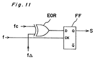
- Fig. 11 is a schematic diagram showing an example of a balanced modulator using.an exclusive OR gate and a flip flop.
- Referring to Fig. 5, an
oscillator 9 generates an original pulse train of a frequency f to a 1/2frequency divider 10 composed of flip-flops (not shown) in which each output pulse of theoscillator 9 is shaped into a rectangular shape pulse with 50% of on-off duty. The output pulses of thefrequency divider 10 are fed to amodulation circuit 11 as a signal fc to be modulated. The output pulses of theoscillator 9 are fed to avariable frequency divider 12 in which the frequency of the original pulses is divided by a predetermined frequency ratio indicated by a frequency change signal mentioned later. The output pulses of thevariable frequency divider 12 are further converted into a rectangular shape pulses with 50% duty in a second 1/2frequency divider 13 and the converted pulses are fed to amodulation circuit 11 as a modulation signal f Δ . In themodulation circuit 11, the signal fc to be modulated fed from the first 1/2frequency divider 10 is modulated by the modulation signal f A fed from the second 1/2frequency divider 13. It is not essential that the clock frequency for deciding the print data speed (referred to as print speed clock frequency hereinafter) coincides accurately with the bright point speed rate as shown in Fig. 3 but it may be sufficient to make the clock frequency nearly equal the bright point speed rate stepwisely. Thus, in athird frequency divider 14, the frequency dividing ratio is set to divide the scanning period of the printing area equally sixteenth as shown in Fig. 7. Afourth frequency divider 15 counts the 16 time blocks using the output of thethird frequency divider 14 and produces the output of the result of the count in a form of 16 system number. Apolarity reversing circuit 16 is composed of a plurality of exclusive OR gates 16' so that thecircuit 16 acts as the inverters connected to the three channels QA, QB and QC when the output QD of thefourth frequency divider 15, which is applied to thepolarity reversing circuit 16 is low level and as the buffers connected to the three channels when the output QD is high level, thereby resulting in reversing the polarity with respect to the center S of thephotosensitive member 3. - As the
modulation circuit 11 an amplitude modulation circuit is used. In case the modulation signal f A and the signal fc to be modulated are respectively sine wave, the output signal S of themodulation circuit 11 can be expressed as
modulation circuit 11 has such frequency distribution as shown in Fig. 7. The frequency fc + f Acan be derived from the frequency components by aband pass filter 18. In order to obtain a good result, preferably a balanced modulator may be used as themodulation circuit 11. In case the balanced modulator is used the output signal S is expressed by
band pass filter 11 may be easier. - Although various types of balanced modulators are commercially available, in the preferred embodiment of the present invention, the balanced modulator may be composed of an exclusive OR gate EOR and a flip flop FF which can operate under digital mode as shown in Fig. 11. Therefore, the modulation signal f Δ and the signal fc to be modulated must be rectangular wave which is composed of the base frequency and its odd harmonic waves. Therefore, the output signal S of the
modulation circuit 11 is expressed as
- In the above equation by performing the above mentioned conversion to the respective multiplication of the sine terms, the frequency distribution near the modulation signal fc becomes such frequency distribution as shown in Fig. 9 and no problem occurs in the actual use. A desired signal may have a slight displacement of the frequency component near the frequency of fc + f Δdue to the operation of the
variable frequency divider 10. However, the desired signal can be obtained by theband pass filter 18 so far as theband pass filter 18 has the frequency characteristic Bp shown in the dotted line in Fig. 10 The ideal characteristic of theband pass filter 18 is such that only the frequency fc + f Acan be derived but the frequency component higher than fc + 3f Aand frequency component lower than fc - f Aare excluded. The output signal of sine wave of theband pass filter 18 is converted into a pulse signal by thewave shaping circuit 19 so as to produce the clock frequency signal f0 for printing as shown in Fig. 7. The ratio frequency f0 in Fig. 7 shows the ratio of the frequencies at various position on thephotosensitive member 3 with the frequency of the center of thephotosensitive member 8 defined 1 and as shown in the lower half portion of Fig. 7, the ratio frequency is expressed in the stepped manner approximating to the light spot speed ratio shown in Fig. 3. It is noted that in Fig. 7, 015 and 016 represent the outputs of thedividers divider 12. - As the printing speed is controlled by the clock frequency signal, the printing speed can be changed corresponding to the light spot speed, whereby the dot pitch becomes uniform independent of the position of the photosensitive member even if the f-
θ lens 6 is omitted as shown in Fig. 6. In Fig. 6, like parts similar to Fig. 1 are represented by like reference numerals.
Claims (4)
Applications Claiming Priority (2)
| Application Number | Priority Date | Filing Date | Title |
|---|---|---|---|
| JP60169149A JPS6229361A (en) | 1985-07-30 | 1985-07-30 | Frequency fine tuning circuit for laser printer |
| JP169149/85 | 1985-07-30 |
Publications (3)
| Publication Number | Publication Date |
|---|---|
| EP0210618A2 true EP0210618A2 (en) | 1987-02-04 |
| EP0210618A3 EP0210618A3 (en) | 1987-09-16 |
| EP0210618B1 EP0210618B1 (en) | 1990-11-28 |
Family
ID=15881192
Family Applications (1)
| Application Number | Title | Priority Date | Filing Date |
|---|---|---|---|
| EP86110354A Expired - Lifetime EP0210618B1 (en) | 1985-07-30 | 1986-07-26 | Frequency converter for use in a laser printer |
Country Status (5)
| Country | Link |
|---|---|
| US (1) | US4725967A (en) |
| EP (1) | EP0210618B1 (en) |
| JP (1) | JPS6229361A (en) |
| CA (1) | CA1260073A (en) |
| DE (1) | DE3675836D1 (en) |
Cited By (4)
| Publication number | Priority date | Publication date | Assignee | Title |
|---|---|---|---|---|
| EP0356286A1 (en) * | 1988-08-03 | 1990-02-28 | Societe D'applications Generales D'electricite Et De Mecanique Sagem | Multiple resolution laser printor |
| EP0375429A2 (en) * | 1988-12-22 | 1990-06-27 | Xerox Corporation | Digital printers |
| EP0503643A2 (en) * | 1991-03-12 | 1992-09-16 | Mita Industrial Co. Ltd. | Video clock generating circuit and horizontal synchronizing signal generating device in image forming apparatus using laser beam |
| CN103499433A (en) * | 2013-09-30 | 2014-01-08 | 中国科学院西安光学精密机械研究所 | Distortion calibration device and method for f-theta optical system |
Families Citing this family (8)
| Publication number | Priority date | Publication date | Assignee | Title |
|---|---|---|---|---|
| US4823284A (en) * | 1987-11-16 | 1989-04-18 | Xerox Corporation | High speed VLSI based serial to multiplexed data translator |
| JP2771822B2 (en) * | 1988-10-21 | 1998-07-02 | 株式会社リコー | Light irradiation image forming apparatus |
| US7382929B2 (en) * | 1989-05-22 | 2008-06-03 | Pixel Instruments Corporation | Spatial scan replication circuit |
| US6147699A (en) * | 1998-11-10 | 2000-11-14 | Lexmark International, Inc. | Low electromagnetic emissions and improved signal quality video drive architecture for laser printers |
| JP5026141B2 (en) * | 2007-05-02 | 2012-09-12 | 株式会社リコー | Image forming apparatus and image forming method |
| JP6142567B2 (en) * | 2013-02-22 | 2017-06-07 | ノーリツプレシジョン株式会社 | Pulse motor driving device and pulse motor driving method |
| US9699352B1 (en) * | 2015-12-30 | 2017-07-04 | Lexmark International, Inc. | Laser scanning unit adjusting output power of modulated beam using shading information to reduce scan line energy variation |
| CN111123671A (en) * | 2018-11-01 | 2020-05-08 | 联想图像(天津)科技有限公司 | Frequency conversion circuit, exposure device and printer |
Citations (2)
| Publication number | Priority date | Publication date | Assignee | Title |
|---|---|---|---|---|
| DE2856332A1 (en) * | 1977-12-30 | 1979-07-05 | Fujitsu Ltd | STOP PRINTER |
| US4578689A (en) * | 1984-11-26 | 1986-03-25 | Data Recording Systems, Inc. | Dual mode laser printer |
Family Cites Families (3)
| Publication number | Priority date | Publication date | Assignee | Title |
|---|---|---|---|---|
| JPS5765060A (en) * | 1980-10-09 | 1982-04-20 | Fuji Photo Film Co Ltd | Method and device for laser recording |
| JPS57138266A (en) * | 1981-02-19 | 1982-08-26 | Yokogawa Hokushin Electric Corp | Photoscanner |
| JPS6016058A (en) * | 1983-07-08 | 1985-01-26 | Hitachi Ltd | Optical beam scanning device |
-
1985
- 1985-07-30 JP JP60169149A patent/JPS6229361A/en active Granted
-
1986
- 1986-07-26 DE DE8686110354T patent/DE3675836D1/en not_active Expired - Lifetime
- 1986-07-26 EP EP86110354A patent/EP0210618B1/en not_active Expired - Lifetime
- 1986-07-28 US US06/889,873 patent/US4725967A/en not_active Expired - Lifetime
- 1986-07-30 CA CA000514981A patent/CA1260073A/en not_active Expired
Patent Citations (2)
| Publication number | Priority date | Publication date | Assignee | Title |
|---|---|---|---|---|
| DE2856332A1 (en) * | 1977-12-30 | 1979-07-05 | Fujitsu Ltd | STOP PRINTER |
| US4578689A (en) * | 1984-11-26 | 1986-03-25 | Data Recording Systems, Inc. | Dual mode laser printer |
Cited By (8)
| Publication number | Priority date | Publication date | Assignee | Title |
|---|---|---|---|---|
| EP0356286A1 (en) * | 1988-08-03 | 1990-02-28 | Societe D'applications Generales D'electricite Et De Mecanique Sagem | Multiple resolution laser printor |
| FR2635888A1 (en) * | 1988-08-03 | 1990-03-02 | Sagem | |
| EP0375429A2 (en) * | 1988-12-22 | 1990-06-27 | Xerox Corporation | Digital printers |
| EP0375429A3 (en) * | 1988-12-22 | 1992-04-01 | Xerox Corporation | Digital printers |
| EP0503643A2 (en) * | 1991-03-12 | 1992-09-16 | Mita Industrial Co. Ltd. | Video clock generating circuit and horizontal synchronizing signal generating device in image forming apparatus using laser beam |
| EP0503643A3 (en) * | 1991-03-12 | 1992-11-25 | Mita Industrial Co. Ltd. | Video clock generating circuit and horizontal synchronizing signal generating device in image forming apparatus using laser beam |
| US5331342A (en) * | 1991-03-12 | 1994-07-19 | Mita Industrial Co., Ltd. | Video clock generating circuit and horizontal synchronizing signal generating device in image forming apparatus using laser beam |
| CN103499433A (en) * | 2013-09-30 | 2014-01-08 | 中国科学院西安光学精密机械研究所 | Distortion calibration device and method for f-theta optical system |
Also Published As
| Publication number | Publication date |
|---|---|
| JPS6229361A (en) | 1987-02-07 |
| JPH0528941B2 (en) | 1993-04-27 |
| CA1260073A (en) | 1989-09-26 |
| EP0210618A3 (en) | 1987-09-16 |
| DE3675836D1 (en) | 1991-01-10 |
| EP0210618B1 (en) | 1990-11-28 |
| US4725967A (en) | 1988-02-16 |
Similar Documents
| Publication | Publication Date | Title |
|---|---|---|
| EP0210618A2 (en) | Frequency converter for use in a laser printer | |
| US7656422B2 (en) | Pulse width modulaton device and image forming apparatus | |
| US4140903A (en) | Precision speed control for optical scanners | |
| US6154246A (en) | Image processing apparatus and image forming apparatus | |
| WO1985005750A1 (en) | Apparatus for producing clock signals for scanner | |
| EP1407371B1 (en) | Method and apparatus for reducing printing artifacts of stitched images | |
| US4160939A (en) | Motor speed control system | |
| JPH0614663B2 (en) | Optical scanning device | |
| KR100984238B1 (en) | Oscillator and pll circuit using the same | |
| EP0041982B1 (en) | A method for recording signals on bands by means of laser beams and apparatus for carrying out the method | |
| JP2003025629A (en) | Optical scanner, its scanning method, display and laser printer | |
| JPS58198962A (en) | Scanner for light beam | |
| KR890006860Y1 (en) | Hologram scanner | |
| JPS62281664A (en) | Optical scanner | |
| JPS61173573A (en) | Beam scanning device | |
| JPH0511199A (en) | Optical writing device | |
| JPH0523662B2 (en) | ||
| JPH01106013A (en) | Light beam scanning device | |
| JP3382022B2 (en) | Light beam deflection scanner | |
| JPH04316268A (en) | Scanning beam synchronization controller | |
| Paul | Image data synchronization techniques in rotating polygon scanners | |
| KR890000946B1 (en) | Scan raster jitter correction device | |
| JPH0373908A (en) | Multipoint synchronous system optical writing and recording device | |
| JPS59101220U (en) | optical scanning device | |
| JPH1082963A (en) | Optical scanner |
Legal Events
| Date | Code | Title | Description |
|---|---|---|---|
| PUAI | Public reference made under article 153(3) epc to a published international application that has entered the european phase |
Free format text: ORIGINAL CODE: 0009012 |
|
| AK | Designated contracting states |
Kind code of ref document: A2 Designated state(s): DE GB IT |
|
| 17P | Request for examination filed |
Effective date: 19861230 |
|
| PUAL | Search report despatched |
Free format text: ORIGINAL CODE: 0009013 |
|
| RHK1 | Main classification (correction) |
Ipc: G01D 15/14 |
|
| AK | Designated contracting states |
Kind code of ref document: A3 Designated state(s): DE GB IT |
|
| 17Q | First examination report despatched |
Effective date: 19890811 |
|
| GRAA | (expected) grant |
Free format text: ORIGINAL CODE: 0009210 |
|
| AK | Designated contracting states |
Kind code of ref document: B1 Designated state(s): DE GB IT |
|
| ITF | It: translation for a ep patent filed |
Owner name: JACOBACCI & PERANI S.P.A. |
|
| REF | Corresponds to: |
Ref document number: 3675836 Country of ref document: DE Date of ref document: 19910110 |
|
| PLBE | No opposition filed within time limit |
Free format text: ORIGINAL CODE: 0009261 |
|
| STAA | Information on the status of an ep patent application or granted ep patent |
Free format text: STATUS: NO OPPOSITION FILED WITHIN TIME LIMIT |
|
| 26N | No opposition filed | ||
| ITTA | It: last paid annual fee | ||
| REG | Reference to a national code |
Ref country code: GB Ref legal event code: IF02 |
|
| PGFP | Annual fee paid to national office [announced via postgrant information from national office to epo] |
Ref country code: GB Payment date: 20050720 Year of fee payment: 20 |
|
| PGFP | Annual fee paid to national office [announced via postgrant information from national office to epo] |
Ref country code: DE Payment date: 20050721 Year of fee payment: 20 |
|
| PGFP | Annual fee paid to national office [announced via postgrant information from national office to epo] |
Ref country code: IT Payment date: 20050728 Year of fee payment: 20 |
|
| PG25 | Lapsed in a contracting state [announced via postgrant information from national office to epo] |
Ref country code: GB Free format text: LAPSE BECAUSE OF EXPIRATION OF PROTECTION Effective date: 20060725 |
|
| REG | Reference to a national code |
Ref country code: GB Ref legal event code: PE20 |