EP0211234A2 - Semiconductor device adapted for light emission - Google Patents
Semiconductor device adapted for light emission Download PDFInfo
- Publication number
- EP0211234A2 EP0211234A2 EP86108964A EP86108964A EP0211234A2 EP 0211234 A2 EP0211234 A2 EP 0211234A2 EP 86108964 A EP86108964 A EP 86108964A EP 86108964 A EP86108964 A EP 86108964A EP 0211234 A2 EP0211234 A2 EP 0211234A2
- Authority
- EP
- European Patent Office
- Prior art keywords
- semiconductor
- light
- layer
- component according
- semiconductor component
- Prior art date
- Legal status (The legal status is an assumption and is not a legal conclusion. Google has not performed a legal analysis and makes no representation as to the accuracy of the status listed.)
- Withdrawn
Links
Images

Classifications
-
- H—ELECTRICITY
- H01—ELECTRIC ELEMENTS
- H01L—SEMICONDUCTOR DEVICES NOT COVERED BY CLASS H10
- H01L33/00—Semiconductor devices with at least one potential-jump barrier or surface barrier specially adapted for light emission; Processes or apparatus specially adapted for the manufacture or treatment thereof or of parts thereof; Details thereof
- H01L33/02—Semiconductor devices with at least one potential-jump barrier or surface barrier specially adapted for light emission; Processes or apparatus specially adapted for the manufacture or treatment thereof or of parts thereof; Details thereof characterised by the semiconductor bodies
- H01L33/20—Semiconductor devices with at least one potential-jump barrier or surface barrier specially adapted for light emission; Processes or apparatus specially adapted for the manufacture or treatment thereof or of parts thereof; Details thereof characterised by the semiconductor bodies with a particular shape, e.g. curved or truncated substrate
- H01L33/24—Semiconductor devices with at least one potential-jump barrier or surface barrier specially adapted for light emission; Processes or apparatus specially adapted for the manufacture or treatment thereof or of parts thereof; Details thereof characterised by the semiconductor bodies with a particular shape, e.g. curved or truncated substrate of the light emitting region, e.g. non-planar junction
-
- H—ELECTRICITY
- H01—ELECTRIC ELEMENTS
- H01L—SEMICONDUCTOR DEVICES NOT COVERED BY CLASS H10
- H01L33/00—Semiconductor devices with at least one potential-jump barrier or surface barrier specially adapted for light emission; Processes or apparatus specially adapted for the manufacture or treatment thereof or of parts thereof; Details thereof
- H01L33/0004—Devices characterised by their operation
- H01L33/002—Devices characterised by their operation having heterojunctions or graded gap
- H01L33/0025—Devices characterised by their operation having heterojunctions or graded gap comprising only AIIIBV compounds
-
- H—ELECTRICITY
- H01—ELECTRIC ELEMENTS
- H01L—SEMICONDUCTOR DEVICES NOT COVERED BY CLASS H10
- H01L33/00—Semiconductor devices with at least one potential-jump barrier or surface barrier specially adapted for light emission; Processes or apparatus specially adapted for the manufacture or treatment thereof or of parts thereof; Details thereof
- H01L33/005—Processes
- H01L33/0062—Processes for devices with an active region comprising only III-V compounds
-
- H—ELECTRICITY
- H01—ELECTRIC ELEMENTS
- H01L—SEMICONDUCTOR DEVICES NOT COVERED BY CLASS H10
- H01L2924/00—Indexing scheme for arrangements or methods for connecting or disconnecting semiconductor or solid-state bodies as covered by H01L24/00
- H01L2924/0001—Technical content checked by a classifier
- H01L2924/0002—Not covered by any one of groups H01L24/00, H01L24/00 and H01L2224/00
Definitions
- the invention relates to a light-emitting semiconductor component with a substrate and two semiconductor layers located on the substrate, the conductivity type of one semiconductor layer being opposite to the conductivity type of the other semiconductor layer (opposite conductivity type).
- LED light-emitting diodes
- the known processes for the production of LEDs have certain shortcomings: in the case of production by means of gas phase epitaxy of GaAs 1-x P x and p-diffusion of the active regions, small-area and closely adjacent LEDs can be produced in a simple manner, but that is Radiation power of the elements obtained is relatively low. For example, a typical LED made of GaAs 0.6 P 0.4 emits a power of approximately 25 ⁇ W at an operating current of 10 mA. With another known manufacturing method, the liquid phase epitaxy of Ga 1-x Al x As, red LEDs can be obtained with significantly higher power those that emit more than 100 ⁇ W under the same conditions. With this technique, however, it is disadvantageous that the active pn junction is formed on the entire semiconductor wafer.
- the invention is based on the object of specifying a light-emitting semiconductor component which has a small-area active region, which emits high power and which can be produced using relatively simple means. This object is achieved in a light-emitting semiconductor component of the type mentioned at the outset according to the invention by the characterizing features of claim 1.
- the invention is explained below using two exemplary embodiments, the first exemplary embodiment being a small-area individual element for fiber-optic applications.
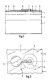
- the manufacture of the first exemplary embodiment is described with reference to FIGS. 1 and 2.
- a first layer 2 of gallium aluminum arsenide Ga 1-x Al x As is deposited by means of liquid phase epitaxy, which is also p-type, e.g. B. by doping with zinc in the range 1018 to 1019 cm ⁇ 3, and which has a thickness of 10 to 50 microns, preferably around 20 microns.
- the aluminum content x of layer 2 is depending on the desired ter wavelength selected in the range 0 to 45%. So corresponds to B. an aluminum content of 10%, a wavelength of about 800 nm and an aluminum content of 40%, a wavelength of about 650 nm.
- a layer 2 is formed on the layer 2 second layer 3 also deposited from gallium aluminum arsenide Ga 1-y Al y As in the same way, which is n-type, e.g. B. by doping with tellurium in the range 1017 to 1018 cm ⁇ 3 and which has a thickness of 3 to 20 microns, preferably around 5 microns.
- FIG. 1 shows the production of only one component, while in reality, of course, a large number of individual elements are produced at the same time.
- p-type zones 5 are now produced, the depth of which is 7 ⁇ m, for example, with a thickness of the second epitaxial layer 3 of 5 ⁇ m. After this diffusion process, only the regions under the circular regions of the masking layer 4 are n-conductive in the layer 3. These areas have a diameter of approximately 45 ⁇ m. Now an insulation layer 6 is applied, the z. B.
- the second exemplary embodiment is described below with reference to FIGS. 3 (cross section) and 4 (top view).
- the substrate 1, first layer 2 and second layer 3 correspond completely to the first embodiment.
- the further production steps are also very similar to the first exemplary embodiment, the structures differ only in the lateral direction, i. H. parallel to the layer surfaces. Rectangular areas are formed from the masking layer 4 for each element of the monolithic LED row to be produced.
- the p-type regions 5 form insulating regions between the n-type regions lying under the rectangular regions of the masking layer 4.
- the contact openings 7 in the insulation layer 6 connect the metallic contact layer 8 to the n-type regions.
- the bonding surfaces 9 are placed alternately to one and the other side of the LED row in order to provide sufficient space for attaching the bonding wires even with a small size and small distance between the LED elements.
- the width of the n-type areas z. B. be about 40 microns.
Abstract
Description
Die Erfindung betrifft ein lichtemittierendes Halbleiterbauelement mit einem Substrat und zwei auf dem Substrat befindlichen Halbleiterschichten, wobei der Leitungstyp der einen Halbleiterschicht entgegengesetzt zum Leitungstyp der anderen Halbleiterschicht ist (entgegengesetzter Leitungstyp).The invention relates to a light-emitting semiconductor component with a substrate and two semiconductor layers located on the substrate, the conductivity type of one semiconductor layer being opposite to the conductivity type of the other semiconductor layer (opposite conductivity type).
Anordnungen mit lichtemittierenden Dioden (LED) werden heute für sehr viele verschiedenartige Anwendungen eingesetzt. Zwei Anwendungsmöglichkeiten haben in der letzten Zeit besonders an Bedeutung gewonnen und zwar kleinflächige LED's (aktive Fläche typisch 50 µm Durchmesser) für Lichtleiteranordnungen und LED-Zeilen mit hoher Auflösung (10 bis 16 LED's pro mm) für elektrophotographische Drucker.Arrangements with light-emitting diodes (LED) are used today for many different types of applications. Two possible uses have recently become particularly important: small-area LEDs (active area typically 50 µm in diameter) for light guide arrangements and LED lines with high resolution (10 to 16 LEDs per mm) for electrophotographic printers.
Für beide Fälle weisen die bekannten Verfahren zur Herstellung von LED's bestimmte Mängel auf: bei einer Herstellung mittels Gasphasenepitaxie von GaAs1-xPx und p-Diffusion der aktiven Gebiete können zwar in einfacher Weise kleinflächige und eng benachbarte LED's hergestellt werden, jedoch ist die Strahlungsleistung der erhaltenen Elemente verhältnismäßig gering. Beispielsweise emittiert eine typische LED aus GaAs0,6P0,4 bei einem Betriebsstrom von 10 mA eine Leistung von etwa 25 µW. Mit einer anderen bekannten Herstellungsmethode, der Flüssigphasenepitaxie von Ga1-xAlxAs, können rote LED's erheblich höherer Leistung erhalten wer den, die bei gleichen Bedingungen über 100 µW emittieren. Bei dieser Technik ist es jedoch nachteilig, daß der aktive pn-Übergang auf der ganzen Halbleiterscheibe entsteht. Dadurch wird die Herstellung kleinflächiger und eng benachbarter LED's erschwert und erfordert z. B. die Anwendung der Mesatechnik, so daß Leiterbahnen zur Stromzuführung nur mit erheblichen Schwierigkeiten angebracht werden können. Alternativ könnte auch das Verfahren der selektiven Flüssigphasenepitaxie eingesetzt werden, das aber wenig entwickelt ist und keine hohe Herstellungsausbeute erlaubt.For both cases, the known processes for the production of LEDs have certain shortcomings: in the case of production by means of gas phase epitaxy of GaAs 1-x P x and p-diffusion of the active regions, small-area and closely adjacent LEDs can be produced in a simple manner, but that is Radiation power of the elements obtained is relatively low. For example, a typical LED made of GaAs 0.6 P 0.4 emits a power of approximately 25 µW at an operating current of 10 mA. With another known manufacturing method, the liquid phase epitaxy of Ga 1-x Al x As, red LEDs can be obtained with significantly higher power those that emit more than 100 µW under the same conditions. With this technique, however, it is disadvantageous that the active pn junction is formed on the entire semiconductor wafer. This makes the production of small-area and closely adjacent LEDs difficult and requires z. B. the application of mesa technology, so that conductor tracks for power supply can be attached only with considerable difficulty. Alternatively, the method of selective liquid phase epitaxy could also be used, but this is not very developed and does not allow a high production yield.
Der Erfindung liegt die Aufgabe zugrunde, ein lichtemittierendes Halbleiterbauelement anzugeben, welches ein kleinflächiges aktives Gebiet aufweist, welches hohe Leistung emittiert und welches mit relativ einfachen Mitteln herstellbar ist. Diese Aufgabe wird bei einem lichtemittierenden Halbleiterbauelement der eingangs erwähnten Art nach der Erfindung durch die kennzeichnenden Merkmale des Anspruchs 1 gelöst.The invention is based on the object of specifying a light-emitting semiconductor component which has a small-area active region, which emits high power and which can be produced using relatively simple means. This object is achieved in a light-emitting semiconductor component of the type mentioned at the outset according to the invention by the characterizing features of claim 1.
Die Erfindung wird im folgenden anhand von zwei Ausführungsbeispielen erläutert, wobei das erste Ausführungbeispiel ein kleinflächiges Einzelelement für faseroptische Anwendungen ist. Die Herstellung des ersten Ausführungsbeispiels wird anhand der Figuren 1 und 2 beschrieben.The invention is explained below using two exemplary embodiments, the first exemplary embodiment being a small-area individual element for fiber-optic applications. The manufacture of the first exemplary embodiment is described with reference to FIGS. 1 and 2.
Gemäß der Figur 1 wird zur Herstellung eines lichtemittierenden Halbleiterbauelements auf einem Substrat 1 aus p-leitendem Galliumarsenid eine erste Schicht 2 aus Galliumaluminiumarsenid Ga1-xAlxAs mittels Flüssigphasenepitaxie abgeschieden, die ebenfalls p-leitend ist, z. B. durch Dotierung mit Zink im Bereich 10¹⁸ bis 10¹⁹ cm⁻³, und die eine Dicke von 10 bis 50 µm, vorzugsweise um 20 µm aufweist. Der Aluminiumgehalt x der Schicht 2 wird je nach gewünsch ter Wellenlänge im Bereich 0 bis 45 % gewählt. So entspricht z. B. einem Aluminiumgehalt von 10 % eine Wellenlänge von etwa 800 nm und einem Aluminiumgehalt von 40 % eine Wellenlänge von etwa 650 nm. Auf der Schicht 2 wird gemäß den Figuren 1 und 2 (Figur 1 zeigt den Querschnitt, Figur 2 die Draufsicht) eine zweite Schicht 3 ebenfalls aus Galliumaluminiumarsenid Ga1-yAlyAs auf die gleiche Weise abgeschieden, die n-leitend ist, z. B. durch Dotierung mit Tellur im Bereich 10¹⁷ bis 10¹⁸ cm⁻³ und die eine Dicke von 3 bis 20 µm, vorzugsweise um 5 µm aufweist. Der Aluminiumgehalt y der Schicht 3 wird größer als der Aluminiumgehalt x der Schicht 2 eingestellt, und zwar vorzugsweise so, daß die Beziehung y = x + 30 % annähernd erfüllt ist. Auf die Öberfläche der Schicht 3 wird eine Maskierungsschicht 4, z. B. aus Siliziumnitrid aufgebracht und mit bekannten photolithographischen und Ätzverfahren so strukturiert, daß für jedes Element ein beispielsweise kreisförmiger Bereich von etwa 60 µm Durchmesser vorgesehen ist. Die Figur 1 zeigt aus Darstellungsgründen die Herstellung von nur einem Bauelement, während in Wirklichkeit natürlich gleichzeitig eine Vielzahl von Einzelelementen hergestellt wird. Durch Eindiffusion von Zink nach bekannten Verfahren werden nun p-leitende Zonen 5 erzeugt, deren Tiefe bei einer Dicke der zweiten Epitaxieschicht 3 von 5 µm beispielsweise 7 µm beträgt. Nach diesem Diffusionsprozeß sind in der Schicht 3 nur noch die Gebiete unter den kreisförmigen Bereichen der Maskierungsschicht 4 n-leitend. Diese Gebiete haben einen Durchmesser von etwa 45 µm. Nun wird eine Isolationsschicht 6 aufgebracht, die z. B. aus Siliziumnitrid oder Siliziumdioxid besteht. In diese Schicht werden nach bekannten Verfahren Kontaktöffnungen 7 eingeätzt, die oberhalb des n-leitenden Gebiets der Schicht 3 angeordnet sind. Schließlich wird eine metallische Kontaktschicht 8 aufgebracht und auf bekannte Weise strukturiert, so daß eine Bond fläche 9 entsteht, die mit dem n-leitenden Gebiet der Schicht 3 verbunden ist. Die weiteren Herstellungsschritte sind bekannt und brauchen hier nicht mehr beschrieben zu werden. Sie umfassen insbesondere die Herstellung eines metallischen Kontakts zum Substrat 1 und die Zerteilung der Halbleiterscheibe in Einzelelemente.According to FIG. 1, to produce a light-emitting semiconductor component on a substrate 1 made of p-type gallium arsenide, a
Das zweite Ausführungsbeispiel wird im folgenden anhand der Figuren 3 (Querschnitt) und 4 (Draufsicht) beschrieben. Substrat 1, erste Schicht 2 und zweite Schicht 3 entsprechen dabei vollständig dem ersten Ausführungsbeispiel. Auch die weiteren Herstellungsschritte sind dem ersten Ausführungsbeispiel sehr ähnlich, die Strukturen unterscheiden sich lediglich in lateraler Richtung, d. h. parallel zu den Schichtflächen. Aus der Maskierungsschicht 4 werden für jedes Element der herzustellenden monolithischen LED-Zeile rechteckige Bereiche gebildet. Die p-leitenden Zonen 5 bilden isolierende Gebiete zwischen den unter den rechteckigen Bereichen der Maskierungsschicht 4 liegenden n-leitenden Gebieten. Die Kontaktöffnungen 7 in der Isolierungsschicht 6 verbinden die metallische Kontaktschicht 8 mit den n-leitenden Gebieten. Die Bondflächen 9 sind alternierend zur einen und anderen Seite der LED-Zeile gelegt, um auch bei geringer Größe und kleinem Abstand der LED-Elemente genügend Raum zum Anbringen der Bonddrähte vorzusehen. Für eine Auflösung der LED-Zeile von 16 Elementen pro mm Länge (Rastermaß 62,5 µm) kann die Breite der n-leitenden Gebiete z. B. etwa 40 µm betragen.The second exemplary embodiment is described below with reference to FIGS. 3 (cross section) and 4 (top view). The substrate 1,
Claims (9)
Applications Claiming Priority (2)
| Application Number | Priority Date | Filing Date | Title |
|---|---|---|---|
| DE19853527720 DE3527720A1 (en) | 1985-08-02 | 1985-08-02 | LIGHT-EMITTING SEMICONDUCTOR COMPONENT |
| DE3527720 | 1985-08-02 |
Publications (2)
| Publication Number | Publication Date |
|---|---|
| EP0211234A2 true EP0211234A2 (en) | 1987-02-25 |
| EP0211234A3 EP0211234A3 (en) | 1989-02-08 |
Family
ID=6277479
Family Applications (1)
| Application Number | Title | Priority Date | Filing Date |
|---|---|---|---|
| EP86108964A Withdrawn EP0211234A3 (en) | 1985-08-02 | 1986-07-02 | Semiconductor device adapted for light emission |
Country Status (3)
| Country | Link |
|---|---|
| EP (1) | EP0211234A3 (en) |
| JP (1) | JPS6235585A (en) |
| DE (1) | DE3527720A1 (en) |
Citations (4)
| Publication number | Priority date | Publication date | Assignee | Title |
|---|---|---|---|---|
| FR2386907A1 (en) * | 1977-04-06 | 1978-11-03 | Radiotechnique Compelec | Electroluminescent semiconductor for fibre-optics - has annular quasi isolating region controlling current density in active area of pn junction |
| US4127792A (en) * | 1976-06-01 | 1978-11-28 | Mitsubishi Denki Kabushiki Kaisha | Luminescent semiconductor display device including gate control electrodes |
| JPS55150282A (en) * | 1979-05-11 | 1980-11-22 | Toshiba Corp | Display device |
| GB2095474A (en) * | 1981-03-25 | 1982-09-29 | Western Electric Co | Semiconductor light emitting devices |
-
1985
- 1985-08-02 DE DE19853527720 patent/DE3527720A1/en not_active Ceased
-
1986
- 1986-07-02 EP EP86108964A patent/EP0211234A3/en not_active Withdrawn
- 1986-07-31 JP JP61179010A patent/JPS6235585A/en active Pending
Patent Citations (4)
| Publication number | Priority date | Publication date | Assignee | Title |
|---|---|---|---|---|
| US4127792A (en) * | 1976-06-01 | 1978-11-28 | Mitsubishi Denki Kabushiki Kaisha | Luminescent semiconductor display device including gate control electrodes |
| FR2386907A1 (en) * | 1977-04-06 | 1978-11-03 | Radiotechnique Compelec | Electroluminescent semiconductor for fibre-optics - has annular quasi isolating region controlling current density in active area of pn junction |
| JPS55150282A (en) * | 1979-05-11 | 1980-11-22 | Toshiba Corp | Display device |
| GB2095474A (en) * | 1981-03-25 | 1982-09-29 | Western Electric Co | Semiconductor light emitting devices |
Non-Patent Citations (4)
| Title |
|---|
| IEEE ELECTRON DEVICE LETTERS. Band EDL-2, Nr. 9, September 1981, New York, USA, Seiten 225-227; C.S. HONG et al.: "Controlled Zn diffusion for low threshold narrow stripe GaAlAs/GaAs DH lasers". * |
| JAPANESE JOURNAL OF APPLIED PHYSICS. Band 24, Nr. 6, Teil 2, Juni 1985, Tokyo, Seiten L463-L465; S. SEMURA et al.: "AlGaAs/GaAs buried multiquantum well lasers with a reactive ion etched window facet". * |
| PATENT ABSTRACTS OF JAPAN. Band 5, Nr. 23 (E-45)(695) 12 Februar 1981; & JP-A-55 150 292 (TOKYO SHIBAURA DENKI K.K.) 22-11-1980 * |
| PROCEEDINGS OF THE S.I.D.. Band 21, Nr. 2, 1980, Los Angeles, USA, Seiten 113-125; K.T. BURNETTE et al.: "Multi-mode matrix (MMM) flat-panel led vector-graphic concept demonstrator display". * |
Also Published As
| Publication number | Publication date |
|---|---|
| DE3527720A1 (en) | 1987-02-12 |
| JPS6235585A (en) | 1987-02-16 |
| EP0211234A3 (en) | 1989-02-08 |
Similar Documents
| Publication | Publication Date | Title |
|---|---|---|
| DE3919462C2 (en) | ||
| DE69637167T2 (en) | LED array with high resolution and its manufacturing process | |
| DE2826486A1 (en) | LIGHT EMITTING SEMICONDUCTOR DEVICE AND METHOD FOR MANUFACTURING IT | |
| DE2608562C2 (en) | ||
| DE3644380C2 (en) | LIGHT-EMITTING DEVICE WITH A DISC-SHAPED SEMICONDUCTOR BODY | |
| DE2755433A1 (en) | RADIATION-EMITTING SEMICONDUCTOR DIODE | |
| DE2713298B2 (en) | Semiconductor laser | |
| DE1764155B2 (en) | Method for producing a semiconductor component from a silicon body | |
| DE2509585A1 (en) | SEMICONDUCTOR ELEMENT AND METHOD FOR MANUFACTURING IT | |
| CH633654A5 (en) | SEMICONDUCTOR COMPONENT AND METHOD FOR PRODUCING THE SAME. | |
| DE2643016A1 (en) | PROCESS FOR PRODUCING AN INTEGRATED SEMICONDUCTOR CIRCUIT | |
| DE2812727A1 (en) | METHOD OF MANUFACTURING A DOUBLE HETEROSTRUCTURE INJECTION LASER | |
| EP0002658A2 (en) | Process for manufacturing a semiconductor device | |
| DE7239485U (en) | MONOLITHIC LIGHT DISPLAY WITH A MATRIX FIELD OF LIGHT-EMITTING SEMICONDUCTOR DIODES | |
| DE2600319B2 (en) | Process for the production of a gallium arsenide light-emitting diode | |
| DE2627355B2 (en) | Solid state light emitting device and method for making the same | |
| DE2629785C2 (en) | Semiconductor component | |
| EP0211234A2 (en) | Semiconductor device adapted for light emission | |
| DE3404875A1 (en) | Semiconductor configuration | |
| WO2020239749A1 (en) | Optoelectronic semiconductor component comprising connection regions, and method for producing the optoelectronic semiconductor component | |
| DE2207057A1 (en) | Monolithic semiconductor display device | |
| EP0185854A2 (en) | Buried heterostructure semiconductor laser diode | |
| DE4338187A1 (en) | Light-emitting semiconductor component | |
| DE1957390C (en) | Semiconductor component and method for its manufacture | |
| DE3138804A1 (en) | SEMICONDUCTOR ARRANGEMENT WITH LOCALIZED ELECTROLUMINESCENT DIODES |
Legal Events
| Date | Code | Title | Description |
|---|---|---|---|
| PUAI | Public reference made under article 153(3) epc to a published international application that has entered the european phase |
Free format text: ORIGINAL CODE: 0009012 |
|
| AK | Designated contracting states |
Kind code of ref document: A2 Designated state(s): FR GB IT NL |
|
| PUAL | Search report despatched |
Free format text: ORIGINAL CODE: 0009013 |
|
| AK | Designated contracting states |
Kind code of ref document: A3 Designated state(s): FR GB IT NL |
|
| STAA | Information on the status of an ep patent application or granted ep patent |
Free format text: STATUS: THE APPLICATION IS DEEMED TO BE WITHDRAWN |
|
| 18D | Application deemed to be withdrawn |
Effective date: 19890202 |
|
| RIN1 | Information on inventor provided before grant (corrected) |
Inventor name: GILLESSEN, KLAUS, DR. DIPL.-PHYS. |