EP0213971B1 - Programmable logic array with added array of gates and added output routing flexibility - Google Patents
Programmable logic array with added array of gates and added output routing flexibility Download PDFInfo
- Publication number
- EP0213971B1 EP0213971B1 EP86401085A EP86401085A EP0213971B1 EP 0213971 B1 EP0213971 B1 EP 0213971B1 EP 86401085 A EP86401085 A EP 86401085A EP 86401085 A EP86401085 A EP 86401085A EP 0213971 B1 EP0213971 B1 EP 0213971B1
- Authority
- EP
- European Patent Office
- Prior art keywords
- input
- gates
- output
- electrically coupled
- lines
- Prior art date
- Legal status (The legal status is an assumption and is not a legal conclusion. Google has not performed a legal analysis and makes no representation as to the accuracy of the status listed.)
- Expired - Lifetime
Links
Images


Classifications
-
- H—ELECTRICITY
- H03—ELECTRONIC CIRCUITRY
- H03K—PULSE TECHNIQUE
- H03K19/00—Logic circuits, i.e. having at least two inputs acting on one output; Inverting circuits
- H03K19/02—Logic circuits, i.e. having at least two inputs acting on one output; Inverting circuits using specified components
- H03K19/173—Logic circuits, i.e. having at least two inputs acting on one output; Inverting circuits using specified components using elementary logic circuits as components
- H03K19/177—Logic circuits, i.e. having at least two inputs acting on one output; Inverting circuits using specified components using elementary logic circuits as components arranged in matrix form
- H03K19/17704—Logic circuits, i.e. having at least two inputs acting on one output; Inverting circuits using specified components using elementary logic circuits as components arranged in matrix form the logic functions being realised by the interconnection of rows and columns
- H03K19/17708—Logic circuits, i.e. having at least two inputs acting on one output; Inverting circuits using specified components using elementary logic circuits as components arranged in matrix form the logic functions being realised by the interconnection of rows and columns using an AND matrix followed by an OR matrix, i.e. programmable logic arrays
- H03K19/17712—Logic circuits, i.e. having at least two inputs acting on one output; Inverting circuits using specified components using elementary logic circuits as components arranged in matrix form the logic functions being realised by the interconnection of rows and columns using an AND matrix followed by an OR matrix, i.e. programmable logic arrays one of the matrices at least being reprogrammable
Definitions
- This invention relates to the field of programmable logic array (PLA) integrated circuits.
- PLA programmable logic array
- FIG. 1 illustrates a simple PLA circuit 10. Included in circuit 10 are four input terminals I0 through I3, each of which is coupled to the input lead of a buffer B0 through B3, respectively. Each buffer has an inverting output lead and a noninverting output lead. For example, buffer B0 has an output lead 12a which provides a signal ISO , which is the inverse of the signal present on terminal I0.
- PAL is a registered trademark of Monolithic Memories, Inc., the Assignee of this application.
- Figure 1 illustrates a simple PLA circuit 10. Included in circuit 10 are four input terminals I0 through I3, each of which is coupled to the input lead of a buffer B0 through B3, respectively. Each buffer has an inverting output lead and a noninverting output lead. For example, buffer B0 has an output lead 12a which provides a signal ISO , which is the inverse of the signal present on terminal I0.
- buffer B0 has an output lead 12b, which provides a signal ISO, which is equal to the signal present at terminal I0.
- Each of the output signals from buffers B0 to B3 is presented as an input signal to an AND gate 14a.
- AND gate 14a is an 8- input AND gate, and each of the output leads of buffers B0 to B3 is uniquely coupled to a single input lead of AND gate 14a.
- Figure 2a illustrates the eight input leads to AND gate 14a.
- Figure 2b illustrates AND gate 14a using the more conventional notation.
- fifteen other AND gates 14b and 14p are also connected to the output leads of buffers B0 through B3 in the same manner as AND gate 14a.
- each of AND gates 14a to 14p is coupled to all eight output leads of buffers B0 to B3.
- a purchaser of a PLA circuit has the option of severing the connection between a given buffer output lead and a given AND gate 14a to 14p. In some prior art circuits, this is done by opening a fuse similar to the fuses employed in programmable read only memories. In other prior art circuits this is done during the manufacturing process of the circuit. Regardless of how such connections are severed, the user can cause each AND gate 14a through 14p to provide a unique output signal dependent on a particular set of input signals. The output signals from AND gates 14a through 14p are sometimes referred to as the "product terms".
- the expression "product term” means the logical product resulting from a logical AND operation on a plurality of input signals, e.g., SIGNAL1 . SIGNAL2, while the expression “sum term” means the logical sum, resulting from a logical OR operation performed on a plurality of input signals, e.g., SIGNAL1 + SIGNAL2.
- a first OR gate 16a includes four input leads coupled to the output leads of AND gates 14m, 14n, 14o and 14p. OR gate 16a generates an output signal on an output lead O0 therefrom. Similarly, an OR gate 16b receives output signals from AND gates 14i, 14j, 14k, and 14l and generates an output signal on a lead O1 therefrom.
- programmable circuit 10 provides desired programmable Boolean functions which can be used in a variety of applications.
- a programmable logic circuit which provides "desired programmable Boolean functions" is one which can be programmed by the system designer to provide any of a number of Boolean functions required in a given system design. This semicustom circuit provides an inexpensive replacement for a large number of logic circuits which would otherwise be required.
- different generic types of PLA circuits include different numbers of input terminals and different numbers of output terminals.
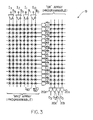
- PLA 19 illustrated in Figure 3.
- the array of OR gates 20a through 20d of PLA 19 are electrically programmably coupled to the output leads of AND gates 14a through 14 p (i.e., the electrical connection between an AND gate and an OR gate can be severed). This is in contrast to PLA circuit 10 of Figure 1 in which the sources of input signals for OR gates 16a through 16d are fixed and nonprogrammable.
- US-A-4 422 072 discloses a PLA comprising a plurality of lines for communicating input signals, a plurality of AND gates, each AND gate having a plurality of input leads programmably electrically coupled to said input lines, and a plurality of OR gates, each input lead of each of these OR gates being programmably electrically coupled to the output lead of an AND gate within said plurality of AND gates.
- PLA's including OR gates with programmable inputs have a number of disadvantages, e.g., they consume a large amount of surface area because of the need to provide additional circuitry to program the OR gate inputs.
- the presence of a large number of input leads to an OR gate creates a large capacitance which slows the OR gate.
- a programmable logic arrray comprising a first plurality of n lines for communicating input signals, first means electrically coupled or programmably electrically coupled to said first plurality of lines for providing a plurality of intermediate signals corresponding to the logical product of some of said input signals, a second plurality of lines, second means electrically coupled or programmably electrically coupled to said first means and said second plurality of lines for generating a plurality of output signals corresponding to the logical sum of some of said intermediate signals, said output signals each being communicated on an associated line within said second plurality of lines, wherein said first means is characterized by comprising: a first plurality of AND gates, each AND gate within said first plurality of AND gates having m input leads, where m is an integer and m ⁇ n, each input lead being programmably electrically coupled to said n lines; and a second plurality of AND gates, each AND gate within said second plurality of AND gates having a plurality of input leads, each input lead being programmably electrically coupled to an output lead
- the AND gates within the first array have a number of input leads, e.g. four, that can be programmably coupled to one of a number of input signal buffer output leads. Because the AND gates only have four input leads, they take up less space than AND gates having a larger number of inputs leads. In addition, in a CMOS implementation of the present invention, AND gates which have a smaller number of input leads are faster than AND gates with a larger number of input leads.
- the PLA of the present invention includes a first array of OR gates and a second array of OR gates.
- the OR gates within the first array of OR gates include a set of input leads (in one embodiment, 3 input leads) each input lead being programmably coupled to an output lead from the second array of AND gates.
- the output leads from the first array of OR gates are programmably electrically coupled to the input leads of a number of the OR gates within the second array of OR gates.
- the OR gates within the second array of OR gates include a set of input leads (in one embodiment 4 input leads). This provides the advantages of being able to generate an output signal which equals the logical sum of 12 different signals without providing 12-input lead OR gates.
- a single OR gate from the first array can be programmably coupled to two OR gates from the second array, thus using the first array of OR gates more economically.
- a bus including a plurality of lines is provided, each line being programmably electrically coupled to the output leads from the second array of OR gates, each line being programmably electrically coupled to each output pin of the PLA circuit.
- FIG. 1 is a schematic diagram of a PLA constructed in accordance with the prior art.
- Figure 2a is a schematic diagram of an AND gate using the notation used in Figure 1.
- Figure 2b is a schematic diagram of an AND gate illustrated in Figure 2a using the more conventional notation.
- Figure 3 is a schematic diagram of a second PLA constructed in accordance with the prior art.
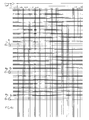
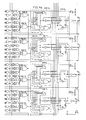
- FIG. 4 is a schematic diagram of a PLA constructed in accordance with the present invention.
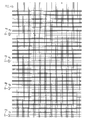
- Figures 5a and 5b are schematic diagrams illustrating the use of various gates within the PLA circuit of figure 4 to generate a various signals.
- a PLA circuit 100 constructed in accordance with the present invention includes several novel features which increase ease of design (i.e., ease of designing a larger system including PLA circuit 100 and determining the interconnections between the logic gates within PLA circuit 100 to provide desired logic functions), enhance flexibility, and permit a more economical use of the gates provided in PLA 100.
- These features include two levels of programmable AND array logic and two levels of programmable OR array logic using product and sum term sharing.
- Other featues of this invention include a four-bit bus 110 which permits routing of output signals from the second programmable layer of OR gates to any output pin desired.
- PLA circuit 100 uses low power CMOS technology and is programmed during the fabrication of the array, as is done in read only memories (ROMS).
- PLA circuit 100 is constructed using other technologies and can be programmed by the purchaser, e.g., by opening fuses as is done in programmable read only memories, or by storing charge on floating gates as is done in electrically programmable read only memory (EPROM) technology.
- EPROM electrically programmable read only memory
- PLA circuit 100 includes a first array of AND gates 102-1 through 102-66, each AND gate having four input leads.
- AND gates 102-1 through 102-66 each AND gate having four input leads.
- AND gates 102-1 through 102-66 are limited to four input leads. This is because in a CMOS implementation AND gates with a small number of input leads are smaller and faster than AND gates with a large number of input leads.
- Each input lead of AND gates 102-1 through 102-66 can be programmably electrically coupled to one of a set of lines L1 to L42. As can be seen, the signals on some of lines L1 through L42 are generated in response to the signals present at a set of input pins IN1 through IN10 as well as the signals present on output pins O1 through O10.
- the customer can determine the interconnections in PLA circuit 100 so that the output signals at pins O1 through O10 as well as the input signals at pins IN1 through IN10 can be used by AND gates 102-1 through 102-66 to generate product terms.
- the signal on line L41 is provided by an OR gate 106-1 and the signal on line L42 is provided by an OR gate 106-22. Lines L41 and L42 can be used to generate signals equal to the logical product of more than 12 signals.
- the signals on line L1 through L42 are input signals to the logic array.
- Each AND gate within AND gates 102-2 through 102-65 is programmably electrically coupled to an input lead of three of AND gates 104-1 through 104-66. (AND gates 102-1 and 102-66 are only programmably electrically coupled to two AND gates within AND gates 104-1 through 104-66). Thus, even though each AND gate within AND gates 102-1 through 102-66 is limited to four input signals, by providing a second group of AND gates 104-1 through 104-66, product terms including as many as 12 input signals can be generated. In addition, as will become apparent in light of the teachings of this specification, product terms generated by a first AND gate, e.g.
- Each AND gate within AND gates 104-1 through 104-66 is programmably electrically coupled to an OR gate within OR gates 106-1 through 106-22.
- OR gates 106-3 through 106-20 are each programmably electrically coupled to two programmable OR gate logic circuits within OR gate logic circuits 108-1 through 108-10.
- the output leads of OR gates 106-1 and 106-2 are only coupled to OR gate logic circuit 108-1, and OR gates 106-21 and 106-22 are only coupled to OR gate logic circuit 108-10.
- Figure 5b is a schematic diagram of gates within PLA 100 which can be programmably interconnected to provide output signals S108-1 and S108-2.
- the term (X1.X2.X3) + (X4.X5) is shared between signals S108-1 and S108-2, it is only necessary to generate this term once and programmably connect this signal to two OR gates (114-1 and 114-2). Because this term does not have to be generated twice, the circuitry that would otherwise be consumed generating this term a second time (e.g. OR gate 106-5 and all the AND gates connected to OR gate 106-5) can be used for other purposes or can be unused. (Gates left unused consume less power than gates being used.)
- each of OR gate logic circuits 108-1 through 108-10 includes a 4-input OR gate such as OR gate 114-1, and two 2 input OR gates such as OR gates 116-1 and 118-1.
- OR gates 116-1 and 118-1 are coupled to an exclusive OR gate 120-1.
- Either OR gate 114-1 or exclusive OR gates 120-1 can be selected in response to system design requirements to generate an output term which is programmably coupled to output pin O1.
- This output term can be presented directly to an inverter 122-1 to provide an inverted signal to output pin O1
- the output term can be inverted by inverter 124-1 and then presented to inverter 122-1 to provide a noninverted signal to output pin O1
- the output term can be stored in flip flop 126-1 and then passed on to inverter 122-1, or the output term can be inverted by inverter 124-1, stored in flip flop 126-1, and passed on to inverter 122-1, depending on system design requirements.
- the output term generated by OR gate logic circuit 108-1 can be coupled to any of the four lines within bus 110 and coupled to any of output pins O2 through O10.
- bus 110 enables a system designer to select his pinout independently of the use of gates within PLA circuit 100.
- bus 110 includes only four lines, in other embodiments bus 110 has a different number of lines.
- PLA circuit 100 receives a signal CLK which is inverted and used to clock flip flops 126-1 through 126-10 via a line 128.
- signal CLK can also be used to generate an input signal for AND gates 102-1 to 102-66 by programmably providing signal CLK to one of the lines within lines L1 through L 42, e.g. lines L3 and L4 via a buffer 30-1. If that is done, and it is desired to use the output signal on pin O1 to generate another one of the signals for lines L1 through L42, output pin O1 can be programmably coupled to a buffer 30-2 which drives two of the lines within lines L1 through L42.
- Buffers 30-1 through 30-10 are also programmably coupled to receive the Q output signal of associated flip flops 126-1 through 126-10.
- pin 31 (normally used to provide a programmable three state control signal for buffers 122-1 through 122-10) can also be used to drive two of the lines L1 through L42 via buffer 30-10. If that is to be the case, the signal present at output pin O10 can be selectively coupled to buffer 30-9 and the output signal at pin O9 can be coupled to buffer 30-8 and so on.
- PLA circuit 100 includes a line 32 coupled to pin IN9.
- Line 32 is coupled to input lead PL of flip flops 126-1 through 126-10 via a zener diode Z.
- a predetermined zener breakdown voltage for example, 12 volts
- a preload signal is presented to input lead PL of each of flip flops 126-1 to 126-10 which causes flip flops 126-1 through 126-10 to store the value present at pins O1 through O10, respectively.
- the flip flops 126-1 to 126-10 can be preset to known states.
- Zener diode Z prevents flip flops 126-1 to 126-10 from storing data present at pins O1 to O10 in response to a high signal at pin IN9 that is less than its zener breakdown voltage.
- Pin IN9 is also used to provide an input signal to buffer B9 which responds to signals having conventional TTL voltage levels. Because of the presence of zener diode Z, a single pin can be used to provide an input signal to buffer B9 that is distinguishable from a preload signal.
- PLA circuit 110 includes a set of lines 134-1 through 134-10, each programmably coupled to the three state control line of buffers 122-1 through 122-10, respectively. Therefore, the signals on lines 134-1 through 134-10 are an alternative means for controlling buffers 122-1 to 122-10.
- Line 134-1 is programmably electrically coupled to the output leads of AND gates 104-2 through 104-8. Lines 134-2 through 134-10 are similarly coupled. Therefore, each of three state buffers 122-1 to 122-10 can be selectively controlled by an associated product term output signal.
- the three state control lines for each of buffers 122-1 through 122-10 can also be programmably connected to ground or VCC to force buffers 122-1 to 122-10 into a high or low impedance mode in response to system design requirements.
Description
- This invention relates to the field of programmable logic array (PLA) integrated circuits.
- Programmable logic array circuits such as the circuits described in the "PAL Programmable Array Logic Handbook" published by Monolithic Memories, Inc., in 1963 are well known in the art. (PAL is a registered trademark of Monolithic Memories, Inc., the Assignee of this application.) Figure 1 illustrates a
simple PLA circuit 10. Included incircuit 10 are four input terminals I₀ through I₃, each of which is coupled to the input lead of a buffer B0 through B3, respectively. Each buffer has an inverting output lead and a noninverting output lead. For example, buffer B0 has anoutput lead 12a which provides a signalISO , which is the inverse of the signal present on terminal I₀. Similarly, buffer B0 has an output lead 12b, which provides a signal ISO, which is equal to the signal present at terminal I₀. Each of the output signals from buffers B0 to B3 is presented as an input signal to anAND gate 14a. ANDgate 14a is an 8- input AND gate, and each of the output leads of buffers B0 to B3 is uniquely coupled to a single input lead ofAND gate 14a. Thus, Figure 2a illustrates the eight input leads toAND gate 14a. Figure 2b illustrates ANDgate 14a using the more conventional notation. In addition fifteen other ANDgates 14b and 14p are also connected to the output leads of buffers B0 through B3 in the same manner asAND gate 14a. Thus, each ofAND gates 14a to 14p is coupled to all eight output leads of buffers B0 to B3. However, a purchaser of a PLA circuit has the option of severing the connection between a given buffer output lead and a given ANDgate 14a to 14p. In some prior art circuits, this is done by opening a fuse similar to the fuses employed in programmable read only memories. In other prior art circuits this is done during the manufacturing process of the circuit. Regardless of how such connections are severed, the user can cause eachAND gate 14a through 14p to provide a unique output signal dependent on a particular set of input signals. The output signals from ANDgates 14a through 14p are sometimes referred to as the "product terms". (As used herein the expression "product term" means the logical product resulting from a logical AND operation on a plurality of input signals, e.g., SIGNAL₁ . SIGNAL₂, while the expression "sum term" means the logical sum, resulting from a logical OR operation performed on a plurality of input signals, e.g., SIGNAL₁ + SIGNAL₂.) - Also, as can be seen in Figure 1, a
first OR gate 16a includes four input leads coupled to the output leads ofAND gates gate 16a generates an output signal on an output lead O₀ therefrom. Similarly, an OR gate 16b receives output signals fromAND gates programmable circuit 10 provides desired programmable Boolean functions which can be used in a variety of applications. As used in this specification, a programmable logic circuit which provides "desired programmable Boolean functions" is one which can be programmed by the system designer to provide any of a number of Boolean functions required in a given system design. This semicustom circuit provides an inexpensive replacement for a large number of logic circuits which would otherwise be required. As is known in the art, different generic types of PLA circuits include different numbers of input terminals and different numbers of output terminals. - Another type of PLA circuit is
PLA 19 illustrated in Figure 3. The array of OR gates 20a through 20d ofPLA 19 are electrically programmably coupled to the output leads ofAND gates 14a through 14 p (i.e., the electrical connection between an AND gate and an OR gate can be severed). This is in contrast toPLA circuit 10 of Figure 1 in which the sources of input signals forOR gates 16a through 16d are fixed and nonprogrammable. - Furthermore, US-A-4 422 072 discloses a PLA comprising a plurality of lines for communicating input signals, a plurality of AND gates, each AND gate having a plurality of input leads programmably electrically coupled to said input lines, and a plurality of OR gates, each input lead of each of these OR gates being programmably electrically coupled to the output lead of an AND gate within said plurality of AND gates.
- However, PLA's including OR gates with programmable inputs have a number of disadvantages, e.g., they consume a large amount of surface area because of the need to provide additional circuitry to program the OR gate inputs. In addition, the presence of a large number of input leads to an OR gate creates a large capacitance which slows the OR gate.
- A programmable logic arrray is provided, comprising a first plurality of n lines for communicating input signals, first means electrically coupled or programmably electrically coupled to said first plurality of lines for providing a plurality of intermediate signals corresponding to the logical product of some of said input signals, a second plurality of lines, second means electrically coupled or programmably electrically coupled to said first means and said second plurality of lines for generating a plurality of output signals corresponding to the logical sum of some of said intermediate signals, said output signals each being communicated on an associated line within said second plurality of lines, wherein said first means is characterized by comprising:
a first plurality of AND gates, each AND gate within said first plurality of AND gates having m input leads, where m is an integer and m < n, each input lead being programmably electrically coupled to said n lines; and
a second plurality of AND gates, each AND gate within said second plurality of AND gates having a plurality of input leads, each input lead being programmably electrically coupled to an output lead of an AND gate within said first plurality of AND gates and each output lead of said second plurality of AND gates being programmably electrically coupled to provide one of said intermediate signals. - In one embodiment of the invention, the AND gates within the first array have a number of input leads, e.g. four, that can be programmably coupled to one of a number of input signal buffer output leads. Because the AND gates only have four input leads, they take up less space than AND gates having a larger number of inputs leads. In addition, in a CMOS implementation of the present invention, AND gates which have a smaller number of input leads are faster than AND gates with a larger number of input leads.
- By providing the second array of AND gates, it is possible to generate a product term of more than four input signals, while preserving the advantage of small AND gates. In addition, if it is desired to provide two product terms with a number of common terms, a single AND gate from the first array can be programmably coupled to two AND gates from the second array, thus using the first array of AND gates more economically.
- The PLA of the present invention includes a first array of OR gates and a second array of OR gates. The OR gates within the first array of OR gates include a set of input leads (in one embodiment, 3 input leads) each input lead being programmably coupled to an output lead from the second array of AND gates. The output leads from the first array of OR gates are programmably electrically coupled to the input leads of a number of the OR gates within the second array of OR gates. The OR gates within the second array of OR gates include a set of input leads (in one embodiment 4 input leads). This provides the advantages of being able to generate an output signal which equals the logical sum of 12 different signals without providing 12-input lead OR gates. In addition, if it is desired to provide two sum terms with a number of common terms, a single OR gate from the first array can be programmably coupled to two OR gates from the second array, thus using the first array of OR gates more economically.
- In accordance with another feature of the present invention, a bus including a plurality of lines is provided, each line being programmably electrically coupled to the output leads from the second array of OR gates, each line being programmably electrically coupled to each output pin of the PLA circuit. This permits greater flexibility in routing output signals to any output pin and therefore also leads to more economical use of the gate contained in the PLA. These and other advantages of the invention are better understood with reference to the drawings below.
- Figure 1 is a schematic diagram of a PLA constructed in accordance with the prior art.
- Figure 2a is a schematic diagram of an AND gate using the notation used in Figure 1.
- Figure 2b is a schematic diagram of an AND gate illustrated in Figure 2a using the more conventional notation.
- Figure 3 is a schematic diagram of a second PLA constructed in accordance with the prior art.
- Figure 4 is a schematic diagram of a PLA constructed in accordance with the present invention.
- Figures 5a and 5b are schematic diagrams illustrating the use of various gates within the PLA circuit of figure 4 to generate a various signals.
- Referring to figure 4, a
PLA circuit 100 constructed in accordance with the present invention includes several novel features which increase ease of design (i.e., ease of designing a larger system includingPLA circuit 100 and determining the interconnections between the logic gates withinPLA circuit 100 to provide desired logic functions), enhance flexibility, and permit a more economical use of the gates provided inPLA 100. These features include two levels of programmable AND array logic and two levels of programmable OR array logic using product and sum term sharing. Other featues of this invention include a four-bit bus 110 which permits routing of output signals from the second programmable layer of OR gates to any output pin desired. - In one embodiment of the invention,
PLA circuit 100 uses low power CMOS technology and is programmed during the fabrication of the array, as is done in read only memories (ROMS). In other embodiments of the invention,PLA circuit 100 is constructed using other technologies and can be programmed by the purchaser, e.g., by opening fuses as is done in programmable read only memories, or by storing charge on floating gates as is done in electrically programmable read only memory (EPROM) technology. As can be seen in figure 4, there are a plurality of boxes (e. g., box 112) interspersed throughout the schematic diagram. These boxes symbolically indicate a programmable electrical connection. Thus, between the output lead from AND gate 102-1 and one of the input leads of AND gate 104-1 is a programmable electrical connection that is either connected or disconnected in response to end user requirements. -
PLA circuit 100 includes a first array of AND gates 102-1 through 102-66, each AND gate having four input leads. (Throughout the specification, reference is made to logic gates having a specific number of input leads. However, it should be understood that these numbers are merely exemplary, and other embodiments of the invention use logic gates having other numbers of input leads.) - Although some prior art PLA's include AND gates having a larger number of input leads, AND gates 102-1 through 102-66 are limited to four input leads. This is because in a CMOS implementation AND gates with a small number of input leads are smaller and faster than AND gates with a large number of input leads. Each input lead of AND gates 102-1 through 102-66 can be programmably electrically coupled to one of a set of lines L1 to L42. As can be seen, the signals on some of lines L1 through L42 are generated in response to the signals present at a set of input pins IN₁ through IN₁₀ as well as the signals present on output pins O₁ through O₁₀. In this way, the customer can determine the interconnections in
PLA circuit 100 so that the output signals at pins O₁ through O₁₀ as well as the input signals at pins IN₁ through IN₁₀ can be used by AND gates 102-1 through 102-66 to generate product terms. As can also be seen in the schematic diagram of Figure 4, the signal on line L41 is provided by an OR gate 106-1 and the signal on line L42 is provided by an OR gate 106-22. Lines L41 and L42 can be used to generate signals equal to the logical product of more than 12 signals. The signals on line L1 through L42 are input signals to the logic array. - Each AND gate within AND gates 102-2 through 102-65 is programmably electrically coupled to an input lead of three of AND gates 104-1 through 104-66. (AND gates 102-1 and 102-66 are only programmably electrically coupled to two AND gates within AND gates 104-1 through 104-66). Thus, even though each AND gate within AND gates 102-1 through 102-66 is limited to four input signals, by providing a second group of AND gates 104-1 through 104-66, product terms including as many as 12 input signals can be generated. In addition, as will become apparent in light of the teachings of this specification, product terms generated by a first AND gate, e.g. AND gate 102-7, can be shared by a plurality of AND gates, e.g., AND gates 104-6, 104-7 and 104-8. This permits more economical use of AND gates because a single product term will not have to be generated twice. To understand why this is so, assume it is desired to produce the following signals :
S104-6 = X1.X2.X3.X4.X5.X6.X7.X8.X9.X10.X11.X12
S104-7 : X9.X10.X11.X12.X.13.X14
where signals S104-6 and S104-7 are generated by AND gates 104-6 and 104-7, respectively, as illustrated in Figure 5a. If signal S104-6 is the signal provided at the output lead of AND gate 104-6, AND gates 102-5, 102-6, and 102-7 are all required to provide input signals to AND gate 104-6. If AND gate 102-7 is used to provide a signal S102-7 = X9.X10.X11.X12, signal S102-7 is provided as an input signal to AND gates 104-6 and 104-7. It is seen that if the output signal from AND gate 102-7 could not be shared by AND gates 104-6 and 104-7, it would be impossible to generate signal S104-7 with AND gate 104-7 because AND gate 104-7 could only be coupled to single 4-input AND gate 102-8. Therefore, because of the unique sharing of the output signals from AND gates 102-1 through 102-66, it is now possible to generate product terms that would otherwise be impossible to generate using an array of 4-input and 3-input AND gates. - Each AND gate within AND gates 104-1 through 104-66 is programmably electrically coupled to an OR gate within OR gates 106-1 through 106-22. OR gates 106-3 through 106-20 are each programmably electrically coupled to two programmable OR gate logic circuits within OR gate logic circuits 108-1 through 108-10. The output leads of OR gates 106-1 and 106-2 are only coupled to OR gate logic circuit 108-1, and OR gates 106-21 and 106-22 are only coupled to OR gate logic circuit 108-10. By coupling the output signals from OR gates 106-3 through 106-20 to two different OR gate logic circuits 108-1 through 108-10, flexibility of design is enhanced. To understand how this is so, assume it is desired to provide signals S108-1 and S108-2 at the output leads of OR gate logic circuits 108-1 and 108-2, respectively, as described below.
S108-1 = (X1.X2.X3)+(X4.X5)+(X6.X7)+(X8.X9)
S108-2 = (X1.X2.X3)+(X4.X5)+(X11.X12)+X13 - Figure 5b is a schematic diagram of gates within
PLA 100 which can be programmably interconnected to provide output signals S108-1 and S108-2. Referring to Figure 5b, because the term (X1.X2.X3) + (X4.X5) is shared between signals S108-1 and S108-2, it is only necessary to generate this term once and programmably connect this signal to two OR gates (114-1 and 114-2). Because this term does not have to be generated twice, the circuitry that would otherwise be consumed generating this term a second time (e.g. OR gate 106-5 and all the AND gates connected to OR gate 106-5) can be used for other purposes or can be unused. (Gates left unused consume less power than gates being used.) - Referring to figure 4, it is seen that each of OR gate logic circuits 108-1 through 108-10 includes a 4-input OR gate such as OR gate 114-1, and two 2 input OR gates such as OR gates 116-1 and 118-1. OR gates 116-1 and 118-1 are coupled to an exclusive OR gate 120-1. Either OR gate 114-1 or exclusive OR gates 120-1 can be selected in response to system design requirements to generate an output term which is programmably coupled to output pin O₁. This output term can be presented directly to an inverter 122-1 to provide an inverted signal to output pin O₁, the output term can be inverted by inverter 124-1 and then presented to inverter 122-1 to provide a noninverted signal to output pin O₁, the output term can be stored in flip flop 126-1 and then passed on to inverter 122-1, or the output term can be inverted by inverter 124-1, stored in flip flop 126-1, and passed on to inverter 122-1, depending on system design requirements. In addition, in accordance with another novel feature of the invention, the output term generated by OR gate logic circuit 108-1 can be coupled to any of the four lines within
bus 110 and coupled to any of output pins O₂ through O₁₀. This is desirable, for example, when a customer has specified a given pinout and the signal to be provided on pin O₂ uses all of AND gates 102-6 through 102-19 (i.e., 14 AND gates) and the signal to be provided on output pin O₃ requires the same number of AND gates within AND gates 102-1 through 102-66. Because of the novel routing feature provided bybus 110, the signal to be provided on output pin O₃ can be generated in a different part of the array, coupled to one ofbus lines 110, and then presented to flip flop 126-3 or inverter 122-3 directly. Thus,bus 110 enables a system designer to select his pinout independently of the use of gates withinPLA circuit 100. Althoughbus 110 includes only four lines, inother embodiments bus 110 has a different number of lines. - In accordance with yet another novel feature of the invention, it is seen that
PLA circuit 100 receives a signal CLK which is inverted and used to clock flip flops 126-1 through 126-10 via aline 128. However, signal CLK can also be used to generate an input signal for AND gates 102-1 to 102-66 by programmably providing signal CLK to one of the lines within lines L1 through L 42, e.g. lines L3 and L4 via a buffer 30-1. If that is done, and it is desired to use the output signal on pin O₁ to generate another one of the signals for lines L1 through L42, output pin O₁ can be programmably coupled to a buffer 30-2 which drives two of the lines within lines L1 through L42. Thus, by selectively programmably coupling each output pin O₁ to O₁₀ to one of two buffers, each buffer driving two of lines L1 through L42, it is possible to use both signal CLK and any nine of the output signals at pins O₁ to O₁₀ as product term input signals. Buffers 30-1 through 30-10 are also programmably coupled to receive theQ output signal of associated flip flops 126-1 through 126-10. - Similarly, it is seen that pin 31 (normally used to provide a programmable three state control signal for buffers 122-1 through 122-10) can also be used to drive two of the lines L1 through L42 via buffer 30-10. If that is to be the case, the signal present at output pin O₁₀ can be selectively coupled to buffer 30-9 and the output signal at pin O₉ can be coupled to buffer 30-8 and so on.
-
PLA circuit 100 includes aline 32 coupled to pin IN₉.Line 32 is coupled to input lead PL of flip flops 126-1 through 126-10 via a zener diode Z. Thus, when the signal atlead 32 reaches a predetermined zener breakdown voltage (for example, 12 volts), a preload signal is presented to input lead PL of each of flip flops 126-1 to 126-10 which causes flip flops 126-1 through 126-10 to store the value present at pins O₁ through O₁₀, respectively. In this way the flip flops 126-1 to 126-10 can be preset to known states. Zener diode Z prevents flip flops 126-1 to 126-10 from storing data present at pins O₁ to O₁₀ in response to a high signal at pin IN₉ that is less than its zener breakdown voltage. Pin IN₉ is also used to provide an input signal to buffer B₉ which responds to signals having conventional TTL voltage levels. Because of the presence of zener diode Z, a single pin can be used to provide an input signal to buffer B₉ that is distinguishable from a preload signal. - It is also noted that
PLA circuit 110 includes a set of lines 134-1 through 134-10, each programmably coupled to the three state control line of buffers 122-1 through 122-10, respectively. Therefore, the signals on lines 134-1 through 134-10 are an alternative means for controlling buffers 122-1 to 122-10. Line 134-1 is programmably electrically coupled to the output leads of AND gates 104-2 through 104-8. Lines 134-2 through 134-10 are similarly coupled. Therefore, each of three state buffers 122-1 to 122-10 can be selectively controlled by an associated product term output signal. It is also noted that the three state control lines for each of buffers 122-1 through 122-10 can also be programmably connected to ground or VCC to force buffers 122-1 to 122-10 into a high or low impedance mode in response to system design requirements.
Claims (22)
- A PLA comprising a first plurality of n lines for communicating input signals, first means electrically coupled or programmably electrically coupled to said first plurality of lines for providing a plurality of intermediate signals corresponding to the logical product of some of said input signals, a second plurality of lines, second means electrically coupled or programmably electrically coupled to said first means and said second plurality of lines for generating a plurality of output signals corresponding to the logical sum of some of said intermediate signals, said output signals each being communicated on an associated line within said second plurality of lines, wherein said first means is characterized by comprising:
a first plurality of AND gates, each AND gate within said first plurality of AND gates having m input leads, where m is an integer and m < n, each input lead being programmably electrically coupled to said n lines; and
a second plurality of AND gates, each AND gate within said second plurality of AND gates having a plurality of input leads, each input lead being programmably electrically coupled to an output lead of an AND gate within said first plurality of AND gates and each output lead of said second plurality of AND gates being programmably electrically coupled to provide one of said intermediate signals. - A PLA as in Claim 1, characterized by comprising:
a plurality of output terminals; and
a third plurality of lines, each output terminal being programmably electrically coupled to each line within said third plurality of lines, each line within said third plurality of lines being programmably electrically coupled to any of said second plurality of lines. - A PLA as in Claim 2, further characterized by comprising:
a plurality of flip flops, each having an output lead programmably electrically coupled to an associated one of said output terminals, each flip flop having an input lead programmably electrically coupled to each of said lines within said third plurality of lines, each flip flop input lead also being programmably electrically coupled to said second means to receive an associated output signal within said plurality of output signals. - The PLA of Claim 2 further characterized by comprising a buffer for providing one of said input signals, said buffer having an input lead programmably electrically coupled to at least two of said output terminals and an output lead electrically coupled to one of the lines within said first plurality of lines.
- The PLA of Claim 4 further characterized by comprising:
an input terminal for receiving an additional input signal;
a buffer having an input lead programmably electrically coupled to said input terminal and one of said output terminals, said buffer providing at least one of said input signals. - The PLA of Claim 4 wherein each of said flip flops includes a clock input lead coupled to said input terminal.
- The PLA of Claim 4 wherein each of said lines within said second plurality of lines is characterized by being programmably electrically coupled to an associated three-state buffer, each associated three-state buffer having an output lead programmably electrically coupled to an associated output terminal, each associated three-state buffer having a three-state control line coupled to said input terminal.
- A PLA as in Claim 1 or 2 wherein said second means is characterized by comprising:
a first plurality of OR gates, each OR gate within said first plurality of OR gates having an input lead coupled or programmably electrically coupled to one of said intermediate signal lines, each OR gate within said first plurality of OR gates having an output lead; and
a second plurality of OR gates, each OR gate within said second plurality of OR gates having a plurality of input leads, each input lead within said plurality of input leads being coupled or programmably coupled to the output lead of one of said OR gates within said first plurality of OR gates, each OR gate within said second plurality of OR gates providing an output signal. - The PLA of Claim 8 wherein the output lead of each OR gate within said first plurality of OR gates is coupled or programmably electrically coupled to the input leads of at least two OR gates within said second plurality of OR gates.
- A PLA as in Claim 1, characterized by comprising:
a plurality of output terminals coupled to said second means, said plurality of output terminals receiving said output signals; and
wherein at least one input line within said plurality of input lines is programmably electrically coupled to two of said output terminals. - The PLA of Claim 1, 2, 10 wherein said plurality of input lines is characterized by including a group of input lines, each input line within said group being programmably electrically coupled to two associated ones of said output terminals.
- The PLA of Claim 10 wherein the programmable electrical coupling between said at least one input line and said two output terminals is characterized by being configured so that said one input line is electrically connected to one of said two output terminals and disconnected from the other of said two output terminals.
- A PLA as in Claims 1, 2, 10 characterized by comprising:
an input terminal;
a three state buffer having an input lead coupled to receive one of said output signals, said buffer having a three state control line coupled to said input terminal;
and wherein one of said input lines is coupled or programmably electrically coupled to said input terminal, said one input line also being coupled or programmably electrically coupled to receive one of said output signals. - The PLA of Claim 13 wherein said one input line is characterized by being coupled or programmably electrically coupled such that said one input line receives either said one output signal or the signal present at said input terminal.
- The PLA of Claim 13 further characterized by comprising a plurality of three state buffers, each of said three state buffers within said plurality having an input lead coupled to receive one of said output signals, each three state buffer within said plurality of three state buffers having a three state control line coupled to said input terminal.
- A PLA as in Claim 1, characterized by comprising:
an input terminal,
a flip flop coupled or programmably electrically coupled to store one of said output signals, said flip flop having a clock input lead coupled to said input terminal,
and wherein one of said input lines is programmably electrically coupled to said input terminal, said one input line also being programmably electrically coupled to receive one of said output signals. - The PLA of Claim 16 further characterized by comprising a plurality of flip flops coupled to store an associated one of said output signals, each flip flop within said plurality having a clock input lead coupled to said input terminal.
- The PLA of Claim 16 wherein said one input line is characterized by being programmably electrically coupled such that said one input line receives either the signal at said input terminal or said one output signal.
- A PLA as in Claim 2, 10, 16 wherein said first means is characterized by comprising:
a group of AND gates having input leads electrically coupled to said first plurality of lines for providing a plurality of intermediate signals corresponding to the logical product of some of said input signals, each AND gate having an output lead, each intermediate signal being provided on the output lead of an associated one of said AND gates; and
wherein said PLA further comprises a three state buffer having a buffer input lead coupled to receive one of said output signals from said second means and a three state control line programmably electrically coupled to the output leads of a plurality of AND gates within said group of AND gates. - The PLA of Claim 19 wherein the programmable electrical coupling between said three state control lead and the output leads of said plurality of AND gates is characterized by being configured so that said three state control lead is connected to the output lead of one of the AND gates within said plurality and disconnected from the output leads of the other AND gates within said plurality.
- A PLA as in Claims 2, 10 and 16 wherein said first means is characterized by comprising:
an array of AND gates, each AND gate including a plurality of input leads programmably electrically coupled to said input lines, each AND gate having an output lead; and
wherein said second means is characterized by comprising a plurality of OR gates having a plurality of OR gate input leads, each OR gate input lead being electrically coupled to the output lead of an associated one of said AND gates, each OR gate providing an OR gate output signal on an OR gate output lead;
said PLA further comprising a plurality of output terminals; and
means for programmably electrically coupling at least one of said OR gate output leads to each of said output terminals. - The PLA of Claim 21 wherein said means for programmably electrically coupling is characterized by comprising a plurality of lines, each output terminal being programmably electrically coupled to each line within said plurality of lines, each line within said plurality of lines being programmably electrically coupled to the OR gate output lead of each OR gate within said plurality of OR gates.
Applications Claiming Priority (2)
| Application Number | Priority Date | Filing Date | Title |
|---|---|---|---|
| US765038 | 1985-08-12 | ||
| US06/765,038 US4758746A (en) | 1985-08-12 | 1985-08-12 | Programmable logic array with added array of gates and added output routing flexibility |
Publications (3)
| Publication Number | Publication Date |
|---|---|
| EP0213971A2 EP0213971A2 (en) | 1987-03-11 |
| EP0213971A3 EP0213971A3 (en) | 1988-12-14 |
| EP0213971B1 true EP0213971B1 (en) | 1992-12-30 |
Family
ID=25072469
Family Applications (1)
| Application Number | Title | Priority Date | Filing Date |
|---|---|---|---|
| EP86401085A Expired - Lifetime EP0213971B1 (en) | 1985-08-12 | 1986-05-22 | Programmable logic array with added array of gates and added output routing flexibility |
Country Status (4)
| Country | Link |
|---|---|
| US (1) | US4758746A (en) |
| EP (1) | EP0213971B1 (en) |
| JP (1) | JP2617447B2 (en) |
| DE (2) | DE213971T1 (en) |
Families Citing this family (126)
| Publication number | Priority date | Publication date | Assignee | Title |
|---|---|---|---|---|
| US5151623A (en) * | 1985-03-29 | 1992-09-29 | Advanced Micro Devices, Inc. | Programmable logic device with multiple, flexible asynchronous programmable logic blocks interconnected by a high speed switch matrix |
| US5225719A (en) * | 1985-03-29 | 1993-07-06 | Advanced Micro Devices, Inc. | Family of multiple segmented programmable logic blocks interconnected by a high speed centralized switch matrix |
| US4763020B1 (en) * | 1985-09-06 | 1997-07-08 | Ricoh Kk | Programmable logic device having plural programmable function cells |
| US4876640A (en) * | 1986-02-07 | 1989-10-24 | Advanced Micro Devices, Inc. | Logic controller having programmable logic "and" array using a programmable gray-code counter |
| US5477165A (en) * | 1986-09-19 | 1995-12-19 | Actel Corporation | Programmable logic module and architecture for field programmable gate array device |
| US5367208A (en) | 1986-09-19 | 1994-11-22 | Actel Corporation | Reconfigurable programmable interconnect architecture |
| JPS6482819A (en) * | 1987-09-25 | 1989-03-28 | Toshiba Corp | Programmable logic array |
| DE3871889T2 (en) * | 1987-10-02 | 1992-12-24 | Kawasaki Steel Co | PROGRAMMABLE INPUT / OUTPUT SWITCHING. |
| DE3875909T2 (en) * | 1987-11-20 | 1993-05-13 | Kawasaki Steel Co | PROGRAMMABLE LOGICAL DEVICE. |
| US4847612A (en) * | 1988-01-13 | 1989-07-11 | Plug Logic, Inc. | Programmable logic device |
| US4871930A (en) * | 1988-05-05 | 1989-10-03 | Altera Corporation | Programmable logic device with array blocks connected via programmable interconnect |
| US4912342A (en) * | 1988-05-05 | 1990-03-27 | Altera Corporation | Programmable logic device with array blocks with programmable clocking |
| JP2548301B2 (en) * | 1988-05-25 | 1996-10-30 | 富士通株式会社 | Programmable logic circuit device |
| US4965472A (en) * | 1988-08-11 | 1990-10-23 | Cypress Semiconductor Corp. | Programmable high speed state machine with sequencing capabilities |
| US5023484A (en) * | 1988-09-02 | 1991-06-11 | Cypress Semiconductor Corporation | Architecture of high speed synchronous state machine |
| US4879481A (en) * | 1988-09-02 | 1989-11-07 | Cypress Semiconductor Corporation | Dual I/O macrocell for high speed synchronous state machine |
| US4894563A (en) * | 1988-10-11 | 1990-01-16 | Atmel Corporation | Output macrocell for programmable logic device |
| US4914322A (en) * | 1988-12-16 | 1990-04-03 | Advanced Micro Devices, Inc. | Polarity option control logic for use with a register of a programmable logic array macrocell |
| US5081375A (en) * | 1989-01-19 | 1992-01-14 | National Semiconductor Corp. | Method for operating a multiple page programmable logic device |
| US4942319A (en) * | 1989-01-19 | 1990-07-17 | National Semiconductor Corp. | Multiple page programmable logic architecture |
| US5021689A (en) * | 1989-01-19 | 1991-06-04 | National Semiconductor Corp. | Multiple page programmable logic architecture |
| JP2566005B2 (en) * | 1989-03-03 | 1996-12-25 | 株式会社東芝 | Input switching device |
| US5047672A (en) * | 1989-03-31 | 1991-09-10 | Texas Instruments Incorporated | ECL/TTL conversion circuit and translation programmable array logic |
| US5457409A (en) * | 1992-08-03 | 1995-10-10 | Advanced Micro Devices, Inc. | Architecture of a multiple array high density programmable logic device with a plurality of programmable switch matrices |
| US5489857A (en) * | 1992-08-03 | 1996-02-06 | Advanced Micro Devices, Inc. | Flexible synchronous/asynchronous cell structure for a high density programmable logic device |
| US5027011A (en) * | 1989-10-31 | 1991-06-25 | Sgs-Thomson Microelectronics, Inc. | Input row drivers for programmable logic devices |
| US5028821A (en) * | 1990-03-01 | 1991-07-02 | Plus Logic, Inc. | Programmable logic device with programmable inverters at input/output pads |
| US5204555A (en) * | 1990-04-05 | 1993-04-20 | Gazelle Microcircuits, Inc. | Logic array having high frequency internal clocking |
| US5198705A (en) * | 1990-05-11 | 1993-03-30 | Actel Corporation | Logic module with configurable combinational and sequential blocks |
| KR930004033B1 (en) * | 1990-08-09 | 1993-05-19 | 현대전자산업 주식회사 | Input/output macro cell of programmable logic element |
| US5245226A (en) * | 1991-02-25 | 1993-09-14 | Lattice Semiconductor Corporation | Output logic macrocell |
| US5416367A (en) * | 1991-03-06 | 1995-05-16 | Quicklogic Corporation | Programmable application specific integrated circuit and logic cell therefor |
| US5122685A (en) * | 1991-03-06 | 1992-06-16 | Quicklogic Corporation | Programmable application specific integrated circuit and logic cell therefor |
| US5338982A (en) * | 1991-03-29 | 1994-08-16 | Kawasaki Steel Corporation | Programmable logic device |
| US5121006A (en) * | 1991-04-22 | 1992-06-09 | Altera Corporation | Registered logic macrocell with product term allocation and adjacent product term stealing |
| US5220214A (en) * | 1991-04-22 | 1993-06-15 | Altera Corporation | Registered logic macrocell with product term allocation and adjacent product term stealing |
| US5861760A (en) | 1991-04-25 | 1999-01-19 | Altera Corporation | Programmable logic device macrocell with improved capability |
| US5384499A (en) * | 1991-04-25 | 1995-01-24 | Altera Corporation | High-density erasable programmable logic device architecture using multiplexer interconnections |
| US5268598A (en) * | 1991-04-25 | 1993-12-07 | Altera Corporation | High-density erasable programmable logic device architecture using multiplexer interconnections |
| US5130574A (en) * | 1991-05-06 | 1992-07-14 | Lattice Semiconductor Corporation | Programmable logic device providing product term sharing and steering to the outputs of the programmable logic device |
| US5191243A (en) * | 1991-05-06 | 1993-03-02 | Lattice Semiconductor Corporation | Output logic macrocell with enhanced functional capabilities |
| US5204556A (en) * | 1991-05-06 | 1993-04-20 | Lattice Semiconductor Corporation | Programmable interconnect structure for logic blocks |
| US5153462A (en) * | 1991-05-21 | 1992-10-06 | Advanced Micro Devices, Inc. | Programmable logic device incorporating voltage comparator |
| US5189320A (en) * | 1991-09-23 | 1993-02-23 | Atmel Corporation | Programmable logic device with multiple shared logic arrays |
| US5250859A (en) * | 1991-09-27 | 1993-10-05 | Kaplinsky Cecil H | Low power multifunction logic array |
| US5359242A (en) * | 1993-01-21 | 1994-10-25 | Altera Corporation | Programmable logic with carry-in/carry-out between logic blocks |
| US5231312A (en) * | 1992-03-12 | 1993-07-27 | Atmel Corporation | Integrated logic circuit with functionally flexible input/output macrocells |
| US5235221A (en) * | 1992-04-08 | 1993-08-10 | Micron Technology, Inc. | Field programmable logic array with speed optimized architecture |
| US5384500A (en) * | 1992-05-15 | 1995-01-24 | Micron Semiconductor, Inc. | Programmable logic device macrocell with an exclusive feedback and an exclusive external input line for a combinatorial mode and accommodating two separate programmable or planes |
| US5220215A (en) * | 1992-05-15 | 1993-06-15 | Micron Technology, Inc. | Field programmable logic array with two or planes |
| US5300830A (en) * | 1992-05-15 | 1994-04-05 | Micron Semiconductor, Inc. | Programmable logic device macrocell with an exclusive feedback and exclusive external input lines for registered and combinatorial modes using a dedicated product term for control |
| US5287017A (en) * | 1992-05-15 | 1994-02-15 | Micron Technology, Inc. | Programmable logic device macrocell with two OR array inputs |
| US5331227A (en) * | 1992-05-15 | 1994-07-19 | Micron Semiconductor, Inc. | Programmable logic device macrocell with an exclusive feedback line and an exclusive external input line |
| US5298803A (en) * | 1992-07-15 | 1994-03-29 | Micron Semiconductor, Inc. | Programmable logic device having low power microcells with selectable registered and combinatorial output signals |
| US5331226A (en) * | 1992-07-23 | 1994-07-19 | Xilinx, Inc. | Logic cell for field programmable gate array having optional input inverters |
| US5386154A (en) * | 1992-07-23 | 1995-01-31 | Xilinx, Inc. | Compact logic cell for field programmable gate array chip |
| US5365125A (en) * | 1992-07-23 | 1994-11-15 | Xilinx, Inc. | Logic cell for field programmable gate array having optional internal feedback and optional cascade |
| US5646547A (en) * | 1994-04-28 | 1997-07-08 | Xilinx, Inc. | Logic cell which can be configured as a latch without static one's problem |
| DE4224804C1 (en) * | 1992-07-27 | 1994-01-13 | Siemens Ag | Programmable logic circuitry |
| WO1994003979A1 (en) * | 1992-07-29 | 1994-02-17 | Xilinx, Inc. | Logic cell for field programmable gate array having optional input inverters |
| EP0584910B1 (en) * | 1992-08-03 | 1996-09-04 | Advanced Micro Devices, Inc. | Programmable logic device |
| US5309046A (en) * | 1992-09-30 | 1994-05-03 | Intel Corporation | Apparatus and method for product term allocation in programmable logic |
| US5341045A (en) * | 1992-11-06 | 1994-08-23 | Intel Corporation | Programmable input buffer |
| US5357153A (en) * | 1993-01-28 | 1994-10-18 | Xilinx, Inc. | Macrocell with product-term cascade and improved flip flop utilization |
| US5324998A (en) * | 1993-02-10 | 1994-06-28 | Micron Semiconductor, Inc. | Zero power reprogrammable flash cell for a programmable logic device |
| US5315177A (en) * | 1993-03-12 | 1994-05-24 | Micron Semiconductor, Inc. | One time programmable fully-testable programmable logic device with zero power and anti-fuse cell architecture |
| US5362999A (en) * | 1993-03-18 | 1994-11-08 | Xilinx, Inc. | EPLD chip with hybrid architecture optimized for both speed and flexibility |
| JPH06276086A (en) * | 1993-03-18 | 1994-09-30 | Fuji Xerox Co Ltd | Field programmable gate array |
| US5311080A (en) * | 1993-03-26 | 1994-05-10 | At&T Bell Laboratories | Field programmable gate array with direct input/output connection |
| US5350954A (en) * | 1993-03-29 | 1994-09-27 | Altera Corporation | Macrocell with flexible product term allocation |
| US5473266A (en) * | 1993-04-19 | 1995-12-05 | Altera Corporation | Programmable logic device having fast programmable logic array blocks and a central global interconnect array |
| DE69315060D1 (en) * | 1993-04-29 | 1997-12-11 | Ibm | Circuit for up and down with primary input for the testability of logical networks |
| US5497107A (en) * | 1993-05-13 | 1996-03-05 | Texas Instruments Incorporated | Multiple, selectable PLAS having shared inputs and outputs |
| US5381058A (en) * | 1993-05-21 | 1995-01-10 | At&T Corp. | FPGA having PFU with programmable output driver inputs |
| US5399922A (en) * | 1993-07-02 | 1995-03-21 | Altera Corporation | Macrocell comprised of two look-up tables and two flip-flops |
| US5410194A (en) * | 1993-08-11 | 1995-04-25 | Xilinx, Inc. | Asynchronous or synchronous load multifunction flip-flop |
| US5506517A (en) * | 1993-09-01 | 1996-04-09 | Lattice Semiconductor Corporation | Output enable structure and method for a programmable logic device |
| US5467029A (en) * | 1993-10-28 | 1995-11-14 | Cypress Semiconductor Corp. | OR array architecture for a programmable logic device |
| US5414376A (en) * | 1993-12-28 | 1995-05-09 | Micron Semiconductor, Inc. | Programmable logic device macrocell having exclusive lines for feedback and external input, and a node which is selectively shared for registered output and external input |
| US5504439A (en) * | 1994-04-01 | 1996-04-02 | Xilinx, Inc. | I/O interface cell for use with optional pad |
| US5600267A (en) * | 1994-06-24 | 1997-02-04 | Cypress Semiconductor Corporation | Apparatus for a programmable CML to CMOS translator for power/speed adjustment |
| KR960706227A (en) * | 1994-09-26 | 1996-11-08 | 요트.게.아. 롤페즈 | Combined programmable logic array and array logic |
| US5568066A (en) * | 1994-11-17 | 1996-10-22 | Advanced Micro Devices, Inc. | Sense amplifier and or gate for a high density programmable logic device |
| US5602494A (en) * | 1995-03-09 | 1997-02-11 | Honeywell Inc. | Bi-directional programmable I/O cell |
| US5489856A (en) * | 1995-03-24 | 1996-02-06 | The United States Of America As Represented By The Director Of The National Security Agency | Laser-programmable clocked-logic integrated-circuit |
| US5625301A (en) * | 1995-05-18 | 1997-04-29 | Actel Corporation | Flexible FPGA input/output architecture |
| US5969539A (en) * | 1995-05-26 | 1999-10-19 | Xilinx, Inc. | Product term exporting mechanism and method improvement in an EPLD having high speed product term allocation structure |
| US5563529A (en) * | 1995-05-26 | 1996-10-08 | Xilinx, Inc. | High speed product term allocation structure supporting logic iteration after committing device pin locations |
| US6531890B1 (en) | 1995-06-02 | 2003-03-11 | Lattice Semiconductor Corporation | Programmable optimized-distribution logic allocator for a high-density complex PLD |
| US5617041A (en) * | 1995-06-02 | 1997-04-01 | Xilinx, Inc. | Method and apparatus for reducing coupling switching noise in interconnect array matrix |
| US5781030A (en) * | 1995-06-02 | 1998-07-14 | Advanced Micro Devices, Inc. | Programmable uniform symmetrical distribution logic allocator for a high-density complex PLD |
| US5521529A (en) * | 1995-06-02 | 1996-05-28 | Advanced Micro Devices, Inc. | Very high-density complex programmable logic devices with a multi-tiered hierarchical switch matrix and optimized flexible logic allocation |
| US5818254A (en) * | 1995-06-02 | 1998-10-06 | Advanced Micro Devices, Inc. | Multi-tiered hierarchical high speed switch matrix structure for very high-density complex programmable logic devices |
| US6028446A (en) * | 1995-06-06 | 2000-02-22 | Advanced Micro Devices, Inc. | Flexible synchronous and asynchronous circuits for a very high density programmable logic device |
| US5723984A (en) * | 1996-06-07 | 1998-03-03 | Advanced Micro Devices, Inc. | Field programmable gate array (FPGA) with interconnect encoding |
| WO1996042140A1 (en) * | 1995-06-09 | 1996-12-27 | Advanced Micro Devices, Inc. | Field programmable gate array (fpga) with interconnect encoding |
| US5610536A (en) * | 1995-09-26 | 1997-03-11 | Xilinx, Inc. | Macrocell architecture with high speed product terms |
| US5600264A (en) * | 1995-10-16 | 1997-02-04 | Xilinx, Inc. | Programmable single buffered six pass transistor configuration |
| US5773994A (en) * | 1995-12-15 | 1998-06-30 | Cypress Semiconductor Corp. | Method and apparatus for implementing an internal tri-state bus within a programmable logic circuit |
| US5848285A (en) * | 1995-12-26 | 1998-12-08 | Cypress Semiconductor Corporation | Macrocell having a dual purpose input register for use in a logic device |
| US5917337A (en) * | 1995-12-29 | 1999-06-29 | Cypress Semiconductor Corp. | Programmable I/O cell with data conversion capability |
| US5811989A (en) * | 1995-12-29 | 1998-09-22 | Cypress Semiconductor Corp. | Programmable I/O cell with data conversion capability |
| US5786710A (en) * | 1995-12-29 | 1998-07-28 | Cypress Semiconductor Corp. | Programmable I/O cell with data conversion capability |
| US5869982A (en) * | 1995-12-29 | 1999-02-09 | Cypress Semiconductor Corp. | Programmable I/O cell with data conversion capability |
| US5760719A (en) * | 1995-12-29 | 1998-06-02 | Cypress Semiconductor Corp. | Programmable I/O cell with data conversion capability |
| US5686844A (en) * | 1996-05-24 | 1997-11-11 | Microchip Technology Incorporated | Integrated circuit pins configurable as a clock input pin and as a digital I/O pin or as a device reset pin and as a digital I/O pin and method therefor |
| US5900742A (en) * | 1996-06-21 | 1999-05-04 | Quicklogic Corporation | Interface cell for a programmable integrated circuit employing antifuses |
| US5936426A (en) * | 1997-02-03 | 1999-08-10 | Actel Corporation | Logic function module for field programmable array |
| GB2330992A (en) * | 1997-11-03 | 1999-05-05 | Nokia Mobile Phones Ltd | Channel estimation in a variable data rate communication system |
| US6069488A (en) * | 1997-11-14 | 2000-05-30 | Xilinx, Inc. | Programmable logic device with versatile exclusive or architecture |
| US6255847B1 (en) | 1998-05-21 | 2001-07-03 | Lattice Semiconductor Corporation | Programmable logic device |
| US6229336B1 (en) | 1998-05-21 | 2001-05-08 | Lattice Semiconductor Corporation | Programmable integrated circuit device with slew control and skew control |
| US6212591B1 (en) | 1999-04-02 | 2001-04-03 | Cradle Technologies | Configurable I/O circuitry defining virtual ports |
| US6259273B1 (en) * | 1999-06-15 | 2001-07-10 | Ict Acquisition Corp. | Programmable logic device with mixed mode programmable logic array |
| US6246258B1 (en) | 1999-06-21 | 2001-06-12 | Xilinx, Inc. | Realizing analog-to-digital converter on a digital programmable integrated circuit |
| JP2002340978A (en) * | 2001-05-10 | 2002-11-27 | Canon Inc | Circuit and method for controlling output |
| US6765408B2 (en) * | 2002-02-11 | 2004-07-20 | Lattice Semiconductor Corporation | Device and method with generic logic blocks |
| US7796464B1 (en) | 2003-06-27 | 2010-09-14 | Cypress Semiconductor Corporation | Synchronous memory with a shadow-cycle counter |
| JP4746969B2 (en) * | 2005-11-24 | 2011-08-10 | Next I&D株式会社 | Twist drill |
| US7893772B1 (en) | 2007-12-03 | 2011-02-22 | Cypress Semiconductor Corporation | System and method of loading a programmable counter |
| US8438522B1 (en) | 2008-09-24 | 2013-05-07 | Iowa State University Research Foundation, Inc. | Logic element architecture for generic logic chains in programmable devices |
| US8661394B1 (en) | 2008-09-24 | 2014-02-25 | Iowa State University Research Foundation, Inc. | Depth-optimal mapping of logic chains in reconfigurable fabrics |
| US8242802B2 (en) * | 2009-04-14 | 2012-08-14 | Via Technologies, Inc. | Location-based bus termination for multi-core processors |
| US10319422B2 (en) | 2015-07-27 | 2019-06-11 | Power Down Semiconductor Inc. | Low power decoder using resonant drive circuitry |
| TWI661676B (en) * | 2018-08-01 | 2019-06-01 | 新唐科技股份有限公司 | Programmable array logic |
| US11784648B2 (en) | 2021-06-02 | 2023-10-10 | Power Down Semiconductor, Inc. | Low power interconnect using resonant drive circuitry |
Family Cites Families (15)
| Publication number | Priority date | Publication date | Assignee | Title |
|---|---|---|---|---|
| US3818252A (en) * | 1971-12-20 | 1974-06-18 | Hitachi Ltd | Universal logical integrated circuit |
| US3936812A (en) * | 1974-12-30 | 1976-02-03 | Ibm Corporation | Segmented parallel rail paths for input/output signals |
| US4124899A (en) * | 1977-05-23 | 1978-11-07 | Monolithic Memories, Inc. | Programmable array logic circuit |
| FR2401561A1 (en) * | 1977-08-26 | 1979-03-23 | Baranik Jury | Switching matrix for programmed machine control - operates with vertical and horizontal rails interconnected via logic gates |
| JPS5483341A (en) * | 1977-12-15 | 1979-07-03 | Nec Corp | Digital integrated circuit |
| US4177452A (en) * | 1978-06-05 | 1979-12-04 | International Business Machines Corporation | Electrically programmable logic array |
| JPS55154832A (en) * | 1979-05-22 | 1980-12-02 | Mitsubishi Electric Corp | Programmable logic circuit |
| JPS57824A (en) * | 1980-05-31 | 1982-01-05 | Matsushita Electric Works Ltd | Breaker with arc gas barrier |
| FR2493641A1 (en) * | 1980-11-03 | 1982-05-07 | Efcis | INTEGRATED LOGIC NETWORK WITH SIMPLIFIED ELECTRICAL PROGRAMMING |
| US4377849A (en) * | 1980-12-29 | 1983-03-22 | International Business Machines Corporation | Macro assembler process for automated circuit design |
| US4422072A (en) * | 1981-07-30 | 1983-12-20 | Signetics Corporation | Field programmable logic array circuit |
| US4506341A (en) * | 1982-06-10 | 1985-03-19 | International Business Machines Corporation | Interlaced programmable logic array having shared elements |
| US4488230A (en) * | 1982-12-08 | 1984-12-11 | At&T Bell Laboratories | Programmed logic array with external signals introduced between its AND plane and its OR plane |
| US4577190A (en) * | 1983-04-11 | 1986-03-18 | At&T Bell Laboratories | Programmed logic array with auxiliary pull-up means to increase precharging speed |
| US4642487A (en) * | 1984-09-26 | 1987-02-10 | Xilinx, Inc. | Special interconnect for configurable logic array |
-
1985
- 1985-08-12 US US06/765,038 patent/US4758746A/en not_active Expired - Lifetime
-
1986
- 1986-04-01 JP JP61075409A patent/JP2617447B2/en not_active Expired - Lifetime
- 1986-05-22 DE DE198686401085T patent/DE213971T1/en active Pending
- 1986-05-22 EP EP86401085A patent/EP0213971B1/en not_active Expired - Lifetime
- 1986-05-22 DE DE8686401085T patent/DE3687383T2/en not_active Expired - Fee Related
Non-Patent Citations (1)
| Title |
|---|
| S.L. HURST: "The Logical Processing of Digital Signals", 1978, CRANE, RUSSAK & COMPANY, New York, pp 347-352 * |
Also Published As
| Publication number | Publication date |
|---|---|
| DE3687383T2 (en) | 1993-04-29 |
| JPS6239913A (en) | 1987-02-20 |
| EP0213971A2 (en) | 1987-03-11 |
| EP0213971A3 (en) | 1988-12-14 |
| DE213971T1 (en) | 1988-04-28 |
| US4758746A (en) | 1988-07-19 |
| JP2617447B2 (en) | 1997-06-04 |
| DE3687383D1 (en) | 1993-02-11 |
Similar Documents
| Publication | Publication Date | Title |
|---|---|---|
| EP0213971B1 (en) | Programmable logic array with added array of gates and added output routing flexibility | |
| US6191611B1 (en) | Driver circuitry for programmable logic devices with hierarchical interconnection resources | |
| US4684830A (en) | Output circuit for a programmable logic array | |
| US5808479A (en) | High speed programmable logic architecture | |
| US5523706A (en) | High speed, low power macrocell | |
| US5473266A (en) | Programmable logic device having fast programmable logic array blocks and a central global interconnect array | |
| EP0450811B1 (en) | Integrated circuit | |
| US5444394A (en) | PLD with selective inputs from local and global conductors | |
| US5341044A (en) | Flexible configuration logic array block for programmable logic devices | |
| EP0746103B1 (en) | Programmable logic array integrated circuits | |
| EP0410759B1 (en) | Configurable logic array and method | |
| US4933577A (en) | Output circuit for a programmable logic array | |
| US5371422A (en) | Programmable logic device having multiplexers and demultiplexers randomly connected to global conductors for interconnections between logic elements | |
| US5504440A (en) | High speed programmable logic architecture | |
| EP0748049B1 (en) | Interconnection architecture for coarse-grained programmable logic device | |
| US5436575A (en) | Programmable logic array integrated circuits | |
| US6810513B1 (en) | Method and apparatus of programmable interconnect array with configurable multiplexer | |
| US5773994A (en) | Method and apparatus for implementing an internal tri-state bus within a programmable logic circuit | |
| EP0613249A1 (en) | Custom look-up table with reduced number of architecture bits | |
| US4983959A (en) | Logic output macrocell | |
| US5614844A (en) | High speed programmable logic architecture | |
| US20020130681A1 (en) | Programmable logic array integrated circuits | |
| EP0343968A2 (en) | Programmable logic device | |
| US6255847B1 (en) | Programmable logic device | |
| US6344989B1 (en) | Programmable logic devices with improved content addressable memory capabilities |
Legal Events
| Date | Code | Title | Description |
|---|---|---|---|
| PUAI | Public reference made under article 153(3) epc to a published international application that has entered the european phase |
Free format text: ORIGINAL CODE: 0009012 |
|
| AK | Designated contracting states |
Kind code of ref document: A2 Designated state(s): DE FR GB NL |
|
| EL | Fr: translation of claims filed | ||
| TCNL | Nl: translation of patent claims filed | ||
| DET | De: translation of patent claims | ||
| PUAL | Search report despatched |
Free format text: ORIGINAL CODE: 0009013 |
|
| AK | Designated contracting states |
Kind code of ref document: A3 Designated state(s): DE FR GB NL |
|
| 17P | Request for examination filed |
Effective date: 19890306 |
|
| RAP1 | Party data changed (applicant data changed or rights of an application transferred) |
Owner name: ADVANCED MICRO DEVICES, INC. |
|
| 17Q | First examination report despatched |
Effective date: 19900129 |
|
| GRAA | (expected) grant |
Free format text: ORIGINAL CODE: 0009210 |
|
| AK | Designated contracting states |
Kind code of ref document: B1 Designated state(s): DE FR GB NL |
|
| PG25 | Lapsed in a contracting state [announced via postgrant information from national office to epo] |
Ref country code: NL Effective date: 19921230 |
|
| REF | Corresponds to: |
Ref document number: 3687383 Country of ref document: DE Date of ref document: 19930211 |
|
| EN | Fr: translation not filed | ||
| PG25 | Lapsed in a contracting state [announced via postgrant information from national office to epo] |
Ref country code: FR Effective date: 19930521 |
|
| NLV1 | Nl: lapsed or annulled due to failure to fulfill the requirements of art. 29p and 29m of the patents act | ||
| PLBE | No opposition filed within time limit |
Free format text: ORIGINAL CODE: 0009261 |
|
| STAA | Information on the status of an ep patent application or granted ep patent |
Free format text: STATUS: NO OPPOSITION FILED WITHIN TIME LIMIT |
|
| 26N | No opposition filed | ||
| REG | Reference to a national code |
Ref country code: FR Ref legal event code: ST |
|
| PGFP | Annual fee paid to national office [announced via postgrant information from national office to epo] |
Ref country code: GB Payment date: 20010404 Year of fee payment: 16 |
|
| PGFP | Annual fee paid to national office [announced via postgrant information from national office to epo] |
Ref country code: DE Payment date: 20010530 Year of fee payment: 16 |
|
| REG | Reference to a national code |
Ref country code: GB Ref legal event code: IF02 |
|
| PG25 | Lapsed in a contracting state [announced via postgrant information from national office to epo] |
Ref country code: GB Free format text: LAPSE BECAUSE OF NON-PAYMENT OF DUE FEES Effective date: 20020522 |
|
| PG25 | Lapsed in a contracting state [announced via postgrant information from national office to epo] |
Ref country code: DE Free format text: LAPSE BECAUSE OF NON-PAYMENT OF DUE FEES Effective date: 20021203 |
|
| GBPC | Gb: european patent ceased through non-payment of renewal fee |
Effective date: 20020522 |