EP0220108A2 - Side-wall doping for trench isolation - Google Patents
Side-wall doping for trench isolation Download PDFInfo
- Publication number
- EP0220108A2 EP0220108A2 EP86402221A EP86402221A EP0220108A2 EP 0220108 A2 EP0220108 A2 EP 0220108A2 EP 86402221 A EP86402221 A EP 86402221A EP 86402221 A EP86402221 A EP 86402221A EP 0220108 A2 EP0220108 A2 EP 0220108A2
- Authority
- EP
- European Patent Office
- Prior art keywords
- trench
- substrate
- well
- layer
- wall
- Prior art date
- Legal status (The legal status is an assumption and is not a legal conclusion. Google has not performed a legal analysis and makes no representation as to the accuracy of the status listed.)
- Withdrawn
Links
Images

Classifications
-
- H—ELECTRICITY
- H01—ELECTRIC ELEMENTS
- H01L—SEMICONDUCTOR DEVICES NOT COVERED BY CLASS H10
- H01L27/00—Devices consisting of a plurality of semiconductor or other solid-state components formed in or on a common substrate
-
- H—ELECTRICITY
- H01—ELECTRIC ELEMENTS
- H01L—SEMICONDUCTOR DEVICES NOT COVERED BY CLASS H10
- H01L21/00—Processes or apparatus adapted for the manufacture or treatment of semiconductor or solid state devices or of parts thereof
- H01L21/70—Manufacture or treatment of devices consisting of a plurality of solid state components formed in or on a common substrate or of parts thereof; Manufacture of integrated circuit devices or of parts thereof
- H01L21/71—Manufacture of specific parts of devices defined in group H01L21/70
- H01L21/76—Making of isolation regions between components
- H01L21/763—Polycrystalline semiconductor regions
-
- H—ELECTRICITY
- H01—ELECTRIC ELEMENTS
- H01L—SEMICONDUCTOR DEVICES NOT COVERED BY CLASS H10
- H01L21/00—Processes or apparatus adapted for the manufacture or treatment of semiconductor or solid state devices or of parts thereof
- H01L21/02—Manufacture or treatment of semiconductor devices or of parts thereof
- H01L21/04—Manufacture or treatment of semiconductor devices or of parts thereof the devices having at least one potential-jump barrier or surface barrier, e.g. PN junction, depletion layer or carrier concentration layer
- H01L21/18—Manufacture or treatment of semiconductor devices or of parts thereof the devices having at least one potential-jump barrier or surface barrier, e.g. PN junction, depletion layer or carrier concentration layer the devices having semiconductor bodies comprising elements of Group IV of the Periodic System or AIIIBV compounds with or without impurities, e.g. doping materials
- H01L21/22—Diffusion of impurity materials, e.g. doping materials, electrode materials, into or out of a semiconductor body, or between semiconductor regions; Interactions between two or more impurities; Redistribution of impurities
- H01L21/225—Diffusion of impurity materials, e.g. doping materials, electrode materials, into or out of a semiconductor body, or between semiconductor regions; Interactions between two or more impurities; Redistribution of impurities using diffusion into or out of a solid from or into a solid phase, e.g. a doped oxide layer
- H01L21/2251—Diffusion into or out of group IV semiconductors
- H01L21/2254—Diffusion into or out of group IV semiconductors from or through or into an applied layer, e.g. photoresist, nitrides
- H01L21/2255—Diffusion into or out of group IV semiconductors from or through or into an applied layer, e.g. photoresist, nitrides the applied layer comprising oxides only, e.g. P2O5, PSG, H3BO3, doped oxides
- H01L21/2256—Diffusion into or out of group IV semiconductors from or through or into an applied layer, e.g. photoresist, nitrides the applied layer comprising oxides only, e.g. P2O5, PSG, H3BO3, doped oxides through the applied layer
Definitions
- the field of the invention is the fabrication of integrated circuits having trenches in the substrate for isolation of the integrated circuit elements.
- the invention relates to an improved integrated circuit fabrication process for trench isolation in which the side and bottom of the trench receive an effective field implant by diffusion of an impurity through a thin oxide coating lining the walls of the trench.
- FIG. 1 there is shown in top view a portion of an integrated circuit constructed according to the invention.
- This particular circuit happens to be a portion of a memory cell array, but the principles of the invention may be applied to any other form of integrated circuit.
- Three “islands” referred to by numerals 92, 94 and 96 are located in a "sea" of polysilicon denoted by the numeral 112, each island being surrounded by a layer of silicon oxide 111.
- the invention is addressed at preventing the formation of parasitic channels between these islands as well as between individual elements within an island; such as the drain and source of a transistor.
- the particular circuit elements located on each island are a pair of transistors 102 and 104 sharing a common drain 106 and each having a separate source 105.
- Each source is connected to a capacitor 117 having a first plate 114 formed vertically into the substrate and a ground plate which is formed by polysilicon 112. Connections to the transistors are omitted to provide greater clarity in the drawing, as is a layer of oxide 111 over sources 105.
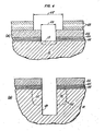
- FIG. 2 there is shown a cross section through line 2-2 of Fig. 1.
- This cross section extends through islands 92 and 94, separated by a trench 120 in the center of the drawing.
- the same two transistors 102 and 104 in each island formed in substrate 101 are shown with capacitor plates 114 on either side of trench 120.
- Trench 120 is lined with oxide 111 which also extends over source 105 and the top of capacitor plate 114.
- Trench 120 is filled with polysilicon 112 which is heavily doped, as is indicated by the P ++ symbol. The polysilicon is protected by a field oxide 115.
- Two capacitors referred to by the general numeral 117, are formed, sharing polysilicon 112 as a common ground plate and having oxide insulation 111 on either side of polysilicon 112.
- the two inner plates 114 complete the structure of transistors 117. Plates 114 are electrically connected by common doping to sources 105.
- a further element in the cross section comprising a doped region having the same polarity as the doping in trench 120 and surrounding trench 120, not only in the plane shown in the cross section but on the surface of the "sea" of polysilicon extending around and facing each island that is above and below the plane of Fig. 2.
- Doped area 121 is not shown as extending into plates 114 of capacitors 117 because the amount of doping is insufficient to change the type of impurity of plates 114.
- the concentration at the edge of oxide 111 is merely reduced slightly.
- FIG. 3 Another side view of the array of islands shown in Fig. 1, looking along line 3-3 in Fig. 1, is shown in Fig. 3.
- the section is taken through one of plates 114 in island 96 and through gate 103 of island 94, showing the bottom of source 105, the plate 114 itself, the oxide 111 that is formed on either side of islands 94 and 96 and extends down into the trench.
- region 121 is shown as extending only up to capacitor plate 114 in island 96, but extends up to gate oxide 109 in island 94.
- This region 121 serves an equivalent function to a conventional field implant by raising the threshold of formation of parasitic channels. These channels can form between islands or along the surface of oxide 111 that faces the island.
- a channel could be formed in region 122, on the vertical surface of oxide 111 that is below the gate of a transistor and between the source and drain, thus effectively short-circuiting the transistor.
- the field implant suppresses the formation of parasitic channels. It has been a drawback of trench isolation methods in the prior art that there has been no effective way to provide the same suppression of the parasitic channels, and this is the problem that the present invention solves.
- the concentration of doped region 121 is indicated by P indicating a light concentration of approximately 5 x 10 16 ions per cc, near the vertical silicon surface in the substrate 101 outside the N + areas, which is formed by diffusion of the heavily doped impurities within polysilicon 112 through oxide 111 and into substrate 101 surrounding the trench. It is necessary, of course, that the impurity used in trench 112 be capable of diffusing through thin oxide. Boron has that property and is a material well known in the art.
- FIG. 4a illustrates a step in an optional version of the invention in which an aperture having a width indicated by the arrow labeled 410, penetrates a series of layers comprising oxide layer 402 having an illustrative thickness of 500 angstroms, nitride layer 404 having an illustrative thickness of 1000 angstroms, and an oxide layer 406 having an illustrative thickness of 5000 angstroms.
- a further photoresist layer 408 having an aperture indicated by the arrow labeled 412 is placed above oxide layer 406 in order to define an ion implant area.
- Aperture 412 is made oversized in order to provide for alignment tolerance.
- a dose of phosphorus is implanted through aperture 410 in the region indicated by the numeral 113 with an illustrative concentration of 10 15 /centimeter 2 .
- Aperture 410 may be formed by any convenient means known in the art, such as by reactive ion etching (RIE).
- RIE reactive ion etching
- Fig. 4b the results of a diffusion drive at a temperature of between 1,100 and 1,150 degrees centigrade for several hours has expanded area 113 into area 113' having a nominal width of 2.1 microns and a nominal depth of 2.5 microns.
- This area 113' which will become plates 114 at capacitor 117, is shown as being penetrated by trench 120 which is formed by a second step of reactive ion etching to a depth of between 3 and 3.5 microns.
- this second RIE step part of oxide layer 406 is consumed.
- Layer 406 need not be oxide, but may be any material that will protect the nitride layer during the RIE step.
- the thickness of layer 406 should, of course, be taken together with the properties of the particular RIE process being used so that the nitride layer 404 is protected during this step.
- the invention is not limited to circuits that employ a capacitor adjacent to the trench and any circuit element may be in that position.
- trench 120 After trench 120 is cut, there are further steps of growing a layer of oxide on the interior surface of trench 120 to a nominal thickness of approximately 400 angstroms; stripping the oxide by a conventional wet etch process and growing a final layer of oxide to a nominal thickness of 100 angstroms.
- the trench is then filled by doped polycrystalline silicon formed in a standard process using, for example SiH 4 together with B 2 H 6 at standard temperatures and pressures well known to those skilled in the art.
- concentration of boron dopant in the polycrystalline silicon should be about 5x10 per cc (typically a factor of 100 greater than the substrate concentration).
- the doped polycrystalline layer has been deposited throughout the trench region, the portion of the polycrystalline silicon lying above the islands is etched away, as is the remainder of oxide layer 406.
- a field oxide region is then grown over polycrystalline silicon 112 to protect the trench and the remainder of the circuit elements on the island are formed in a conventional manner.
- the doped polysilicon 112 in trench 120 is at the same potential as substrate 101, illustratively ground.
- substrate 101 illustratively ground.
- debris could easily cause short circuits or interfere in some other way with the circuit.
- the trench filling material of the same polarity and at the same potential as the substrate any debris will be innocuous.
- capacitor 117 is formed as shown in Fig. 2, then there will be more stress on oxide 111, for a given oxide thickness, when polysilicon 112 is grounded than if it were at Vcc/2, but maintaining capacitor plate 112 at some intermediate voltage would risk shorts to the substrate 101.
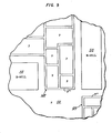
- CMOS circuit The application of the invention to a CMOS circuit is illustrated in Fig. 5, showing a top view of a P-doped epitaxial layer 510 containing N-wells 512 and 513, which are prepared conventionally.
- the N-wells contain circuits that are not indicated in the figure, since the invention is directed at isolation.
- Two networks of trenches 522 and 523, containing P-type polysilicon and formed as discussed above, are shown surrounding islands of P-type silicon containing any circuit elements that it is desirable to isolate.
- the contents of an island could be a single N-channel transistor or a group of N-channel transistors together with other elements, as illustrated in Figs. 1-3.
- the depth of trenches 522 and 523 should be great enough to penetrate the up-diffusion from the substrate. No particular geometry or shape of the trench networks is required. Preferably, the trenches should all have the same width, so that the planarity of the circuit is not affected.
- the circuit elements in the P-doped epitaxial layer could be isolated by conventional planar isolation, with the trenches reserved for a peripheral isolation and latchup protection. Such an arrangement would depend on a tradeoff between the additional complexity of using two isolation schemes and the reliability of the trench isolation process.
- a corresponding network of trench using N-doped polysilicon (Phosporous-doped, say) could be formed within the N-wells. Care would have to be taken to avoid interaction between the N-doped trench filler and the P-doped substrate; and only very high-density circuits that have a great need for compact isolation or that have to employ trench capacitors together with transistors of both polarity would justify the use of trenches in the N-well.
- a further advantageous feature of the invention is that, with polysilicon 112 doped with P-type material and plate 114 and transistor source 105 and drain 106, doped with N-type material, the effect of a pinhole or other defect in oxide 111 is reduced. It is well known that thinner oxides have more holes than thick ones and that the result of a hole is usually a short circuit that ruins the chip. For example, when a conventional five volt level is being stored in a memory cell, the bit line 106, source 105 and capacitor plate 114 of that cell will all be raised to five volts and there is great stress on oxide 111.
- the N+ region will be at plus five volts and the P ++ region will be at ground.
- the region of the circuit around the pinhole will be a P-N diode, reverse-baised at five volts, that will not conduct current. Short circuits through oxide 111 are thus "self-healing", resulting in greater yield than would be the case if a different combination of materials were used.
- the invention has been illustrated in the context of a conventional N-channel process and a DRAM memory cell. Those skilled in the art will readily be able to apply the principles of this invention to other circuits beside DRAMs, and to other combinations of voltage levels and doping materials.
- the point in the process sequence at which the trench is cut and filled is not critical. Preparation of transistor substrates by ion implantation of the channel and other steps up to forming the gates and the sources and drains may be done before or after the trench is cut and filled. The trench must be completed, of course, before interconnections are made between the islands.
Abstract
Description
- The field of the invention is the fabrication of integrated circuits having trenches in the substrate for isolation of the integrated circuit elements.
- The use of trenches for isolation of elements on integrated circuits has been studied for some years. A convenient summary is an article by R. D. Rung entitled "Trench Isolation Prospects for Application in CMOS VLSI". This article appeared in the IEDM 84 Conference in 1984. This article indicates that there is a significant problem associated with the trench isolation process in that it is not practical to perform what is essentially a field implant of the trench bottom and/or side-wall to prevent inversion of the substrate and the formation of parasitic channels. This problem has been addressed by the present invention.
- The invention relates to an improved integrated circuit fabrication process for trench isolation in which the side and bottom of the trench receive an effective field implant by diffusion of an impurity through a thin oxide coating lining the walls of the trench.
- Brief Description of Drawings
- Fig. 1 illustrates a top view of portion of an integrated circuit constructed according to the invention.
- Fig. 2 illustrates a cross section of one element of the invention.
- Fig. 3 illustrates a cross section of a different view of the elements shown in Fig. 1.
- Figs. 4a and 4b illustrate intermediate steps in the fabrication of a trench according to the invention.
- Fig. 5 illustrates a portion of a CMOS circuit employing the invention.
- The importance of having a field implant or doping under oxide isolation in order to prevent the formation of parasitic channels is long established in the art. Previous work on trench isolation, in contrast to the planar isolation that is standard in industry practice, has been troubled by the difficulty in performing something equivalent to a field implant in order to suppress similar parasitic channels.
- Referring now to Fig. 1, there is shown in top view a portion of an integrated circuit constructed according to the invention. This particular circuit happens to be a portion of a memory cell array, but the principles of the invention may be applied to any other form of integrated circuit. Three "islands" referred to by
numerals numeral 112, each island being surrounded by a layer ofsilicon oxide 111. The invention is addressed at preventing the formation of parasitic channels between these islands as well as between individual elements within an island; such as the drain and source of a transistor. The particular circuit elements located on each island are a pair oftransistors common drain 106 and each having aseparate source 105. Each source is connected to acapacitor 117 having afirst plate 114 formed vertically into the substrate and a ground plate which is formed bypolysilicon 112. Connections to the transistors are omitted to provide greater clarity in the drawing, as is a layer ofoxide 111 oversources 105. - Referring now to Fig. 2, there is shown a cross section through line 2-2 of Fig. 1. This cross section extends through
islands trench 120 in the center of the drawing. The same twotransistors substrate 101 are shown withcapacitor plates 114 on either side oftrench 120. Trench 120 is lined withoxide 111 which also extends oversource 105 and the top ofcapacitor plate 114.Trench 120 is filled withpolysilicon 112 which is heavily doped, as is indicated by the P ++ symbol. The polysilicon is protected by afield oxide 115. Two capacitors, referred to by thegeneral numeral 117, are formed, sharingpolysilicon 112 as a common ground plate and havingoxide insulation 111 on either side ofpolysilicon 112. The twoinner plates 114 complete the structure oftransistors 117.Plates 114 are electrically connected by common doping tosources 105. - There is a further element in the cross section, indicated by the
numeral 121, comprising a doped region having the same polarity as the doping intrench 120 and surroundingtrench 120, not only in the plane shown in the cross section but on the surface of the "sea" of polysilicon extending around and facing each island that is above and below the plane of Fig. 2.Doped area 121 is not shown as extending intoplates 114 ofcapacitors 117 because the amount of doping is insufficient to change the type of impurity ofplates 114. The concentration at the edge ofoxide 111 is merely reduced slightly. - Another side view of the array of islands shown in Fig. 1, looking along line 3-3 in Fig. 1, is shown in Fig. 3. There, the section is taken through one of
plates 114 inisland 96 and throughgate 103 ofisland 94, showing the bottom ofsource 105, theplate 114 itself, theoxide 111 that is formed on either side ofislands region 121 is shown as extending only up tocapacitor plate 114 inisland 96, but extends up to gate oxide 109 inisland 94. Thisregion 121 serves an equivalent function to a conventional field implant by raising the threshold of formation of parasitic channels. These channels can form between islands or along the surface ofoxide 111 that faces the island. In particular, a channel could be formed in region 122, on the vertical surface ofoxide 111 that is below the gate of a transistor and between the source and drain, thus effectively short-circuiting the transistor. In planar circuits, the field implant suppresses the formation of parasitic channels. It has been a drawback of trench isolation methods in the prior art that there has been no effective way to provide the same suppression of the parasitic channels, and this is the problem that the present invention solves. The concentration ofdoped region 121 is indicated by P indicating a light concentration of approximately 5 x 10¹⁶ ions per cc, near the vertical silicon surface in thesubstrate 101 outside the N+ areas, which is formed by diffusion of the heavily doped impurities withinpolysilicon 112 throughoxide 111 and intosubstrate 101 surrounding the trench. It is necessary, of course, that the impurity used intrench 112 be capable of diffusing through thin oxide. Boron has that property and is a material well known in the art. - Further details of the process steps can be seen in Figs. 4a and 4b. Fig. 4a illustrates a step in an optional version of the invention in which an aperture having a width indicated by the arrow labeled 410, penetrates a series of layers comprising
oxide layer 402 having an illustrative thickness of 500 angstroms,nitride layer 404 having an illustrative thickness of 1000 angstroms, and anoxide layer 406 having an illustrative thickness of 5000 angstroms. A furtherphotoresist layer 408 having an aperture indicated by the arrow labeled 412 is placed aboveoxide layer 406 in order to define an ion implant area. Aperture 412 is made oversized in order to provide for alignment tolerance. A dose of phosphorus is implanted throughaperture 410 in the region indicated by thenumeral 113 with an illustrative concentration of 10 15/centimeter2.Aperture 410 may be formed by any convenient means known in the art, such as by reactive ion etching (RIE). In Fig. 4b, the results of a diffusion drive at a temperature of between 1,100 and 1,150 degrees centigrade for several hours has expandedarea 113 into area 113' having a nominal width of 2.1 microns and a nominal depth of 2.5 microns. This area 113', which will becomeplates 114 atcapacitor 117, is shown as being penetrated bytrench 120 which is formed by a second step of reactive ion etching to a depth of between 3 and 3.5 microns. In the course of this second RIE step, part ofoxide layer 406 is consumed.Layer 406 need not be oxide, but may be any material that will protect the nitride layer during the RIE step. The thickness oflayer 406 should, of course, be taken together with the properties of the particular RIE process being used so that thenitride layer 404 is protected during this step. The invention is not limited to circuits that employ a capacitor adjacent to the trench and any circuit element may be in that position. - After
trench 120 is cut, there are further steps of growing a layer of oxide on the interior surface oftrench 120 to a nominal thickness of approximately 400 angstroms; stripping the oxide by a conventional wet etch process and growing a final layer of oxide to a nominal thickness of 100 angstroms. - The trench is then filled by doped polycrystalline silicon formed in a standard process using, for example SiH4 together with B2H6 at standard temperatures and pressures well known to those skilled in the art. The concentration of boron dopant in the polycrystalline silicon should be about 5x10 per cc (typically a factor of 100 greater than the substrate concentration). In filling such a deep, narrow trench, there may well develop voids 116 within
polysilicon 112. That is no problem in this invention because the only requirement forpolysilicon 112 is that it form a conductive layer in the region ofcapacitor 117 and have a sufficient amount of polycrystalline silicon in the bottom of the trench to drive a sufficient quantity of boron in to form dopedlayer 121. This amount is non-critical, an advantageous feature of this invention. - After the doped polycrystalline layer has been deposited throughout the trench region, the portion of the polycrystalline silicon lying above the islands is etched away, as is the remainder of
oxide layer 406. A field oxide region is then grown overpolycrystalline silicon 112 to protect the trench and the remainder of the circuit elements on the island are formed in a conventional manner. - It is an advantageous feature of the invention that the doped
polysilicon 112 intrench 120 is at the same potential assubstrate 101, illustratively ground. There will often be small amounts of debris left from previous processing steps in the bottom oftrench 120, which must have a small width to depth ratio in order to occupy as little room as possible. The debris could easily cause short circuits or interfere in some other way with the circuit. With the trench filling material of the same polarity and at the same potential as the substrate, any debris will be innocuous. - If a
capacitor 117 is formed as shown in Fig. 2, then there will be more stress onoxide 111, for a given oxide thickness, whenpolysilicon 112 is grounded than if it were at Vcc/2, but maintainingcapacitor plate 112 at some intermediate voltage would risk shorts to thesubstrate 101. - The application of the invention to a CMOS circuit is illustrated in Fig. 5, showing a top view of a P-doped
epitaxial layer 510 containing N-wells trenches 522 and 523, containing P-type polysilicon and formed as discussed above, are shown surrounding islands of P-type silicon containing any circuit elements that it is desirable to isolate. The contents of an island could be a single N-channel transistor or a group of N-channel transistors together with other elements, as illustrated in Figs. 1-3. For superior latchup protection, the depth oftrenches 522 and 523 should be great enough to penetrate the up-diffusion from the substrate. No particular geometry or shape of the trench networks is required. Preferably, the trenches should all have the same width, so that the planarity of the circuit is not affected. - If desired, the circuit elements in the P-doped epitaxial layer could be isolated by conventional planar isolation, with the trenches reserved for a peripheral isolation and latchup protection. Such an arrangement would depend on a tradeoff between the additional complexity of using two isolation schemes and the reliability of the trench isolation process. Also, a corresponding network of trench using N-doped polysilicon (Phosporous-doped, say) could be formed within the N-wells. Care would have to be taken to avoid interaction between the N-doped trench filler and the P-doped substrate; and only very high-density circuits that have a great need for compact isolation or that have to employ trench capacitors together with transistors of both polarity would justify the use of trenches in the N-well.
- A further advantageous feature of the invention is that, with
polysilicon 112 doped with P-type material andplate 114 andtransistor source 105 and drain 106, doped with N-type material, the effect of a pinhole or other defect inoxide 111 is reduced. It is well known that thinner oxides have more holes than thick ones and that the result of a hole is usually a short circuit that ruins the chip. For example, when a conventional five volt level is being stored in a memory cell, thebit line 106,source 105 andcapacitor plate 114 of that cell will all be raised to five volts and there is great stress onoxide 111. - With this invention, if there is a pinhole through
oxide 111 the N+ region will be at plus five volts and the P++ region will be at ground. The region of the circuit around the pinhole will be a P-N diode, reverse-baised at five volts, that will not conduct current. Short circuits throughoxide 111 are thus "self-healing", resulting in greater yield than would be the case if a different combination of materials were used. - The invention has been illustrated in the context of a conventional N-channel process and a DRAM memory cell. Those skilled in the art will readily be able to apply the principles of this invention to other circuits beside DRAMs, and to other combinations of voltage levels and doping materials. The point in the process sequence at which the trench is cut and filled is not critical. Preparation of transistor substrates by ion implantation of the channel and other steps up to forming the gates and the sources and drains may be done before or after the trench is cut and filled. The trench must be completed, of course, before interconnections are made between the islands.
Claims (9)
Applications Claiming Priority (2)
| Application Number | Priority Date | Filing Date | Title |
|---|---|---|---|
| US78519685A | 1985-10-07 | 1985-10-07 | |
| US785196 | 1985-10-07 |
Publications (2)
| Publication Number | Publication Date |
|---|---|
| EP0220108A2 true EP0220108A2 (en) | 1987-04-29 |
| EP0220108A3 EP0220108A3 (en) | 1990-04-11 |
Family
ID=25134731
Family Applications (1)
| Application Number | Title | Priority Date | Filing Date |
|---|---|---|---|
| EP86402221A Withdrawn EP0220108A3 (en) | 1985-10-07 | 1986-10-07 | Side-wall doping for trench isolation |
Country Status (3)
| Country | Link |
|---|---|
| EP (1) | EP0220108A3 (en) |
| JP (1) | JPS62163338A (en) |
| KR (1) | KR870004517A (en) |
Cited By (3)
| Publication number | Priority date | Publication date | Assignee | Title |
|---|---|---|---|---|
| WO2000013208A2 (en) * | 1998-08-31 | 2000-03-09 | Micron Technology, Inc. | Selectively doped trench device isolation |
| WO2001011682A1 (en) * | 1999-08-09 | 2001-02-15 | Infineon Technologies Ag | Method for producing an insulation |
| DE102006021070B4 (en) * | 2005-05-10 | 2017-06-22 | Infineon Technologies Ag | Semiconductor devices with deep trench isolation structures and methods of making same |
Families Citing this family (1)
| Publication number | Priority date | Publication date | Assignee | Title |
|---|---|---|---|---|
| JP2523712B2 (en) * | 1987-11-25 | 1996-08-14 | 松下電器産業株式会社 | Plasma doping method |
Citations (2)
| Publication number | Priority date | Publication date | Assignee | Title |
|---|---|---|---|---|
| WO1981003241A1 (en) * | 1980-05-07 | 1981-11-12 | Western Electric Co | Silicon integrated circuits |
| WO1986004454A1 (en) * | 1985-01-25 | 1986-07-31 | American Telephone & Telegraph Company | Controlled boron doping of silicon |
-
1986
- 1986-10-07 EP EP86402221A patent/EP0220108A3/en not_active Withdrawn
- 1986-10-07 KR KR1019860008394A patent/KR870004517A/en not_active Application Discontinuation
- 1986-10-07 JP JP61238994A patent/JPS62163338A/en active Pending
Patent Citations (2)
| Publication number | Priority date | Publication date | Assignee | Title |
|---|---|---|---|---|
| WO1981003241A1 (en) * | 1980-05-07 | 1981-11-12 | Western Electric Co | Silicon integrated circuits |
| WO1986004454A1 (en) * | 1985-01-25 | 1986-07-31 | American Telephone & Telegraph Company | Controlled boron doping of silicon |
Non-Patent Citations (4)
| Title |
|---|
| IBM TECHNICAL DISCLOSURE BULLETIN, vol. 18, no. 6, November 1975, pages 1854-1855, New York, US; G.T. GALYON: "Isolation of device components" * |
| IBM TECHNICAL DISCLOSURE BULLETIN, vol. 25, no. 3B, August 1982, pages 1482-1484, New York, US; H.S. BHATIA et al.: "Poly filled trench isolation" * |
| JOURNAL OF THE ELECTROCHEMICAL SOCIETY, vol. 122, no. 12, December 1975, pages 1685-1689; W. VON MUENCH et al.: "Low surface concentration of boron in silicon by diffusion through silicon dioxide" * |
| SOLID-STATE ELECTRONICS, vol. 18, no. 11, November 1975, pages 991-997, Pergamon Press, GB; K. SHIMAKURA et al.: "Boron and phosphorus diffusion through an SiO2 layer from a doped polycrystalline Si source under various drive-in ambients" * |
Cited By (9)
| Publication number | Priority date | Publication date | Assignee | Title |
|---|---|---|---|---|
| WO2000013208A2 (en) * | 1998-08-31 | 2000-03-09 | Micron Technology, Inc. | Selectively doped trench device isolation |
| WO2000013208A3 (en) * | 1998-08-31 | 2000-06-02 | Micron Technology Inc | Selectively doped trench device isolation |
| US6781212B1 (en) | 1998-08-31 | 2004-08-24 | Micron Technology, Inc | Selectively doped trench device isolation |
| EP1473766A2 (en) * | 1998-08-31 | 2004-11-03 | Micron Technology, Inc. | Selectively doped trench device isolation |
| EP1473766A3 (en) * | 1998-08-31 | 2004-12-15 | Micron Technology, Inc. | Selectively doped trench device isolation |
| US7259442B2 (en) | 1998-08-31 | 2007-08-21 | Micron Technology, Inc. | Selectively doped trench device isolation |
| WO2001011682A1 (en) * | 1999-08-09 | 2001-02-15 | Infineon Technologies Ag | Method for producing an insulation |
| US6638814B1 (en) | 1999-08-09 | 2003-10-28 | Infineon Technologies Aktiengesellschaft | Method for producing an insulation |
| DE102006021070B4 (en) * | 2005-05-10 | 2017-06-22 | Infineon Technologies Ag | Semiconductor devices with deep trench isolation structures and methods of making same |
Also Published As
| Publication number | Publication date |
|---|---|
| JPS62163338A (en) | 1987-07-20 |
| EP0220108A3 (en) | 1990-04-11 |
| KR870004517A (en) | 1987-05-11 |
Similar Documents
| Publication | Publication Date | Title |
|---|---|---|
| US4922313A (en) | Process for manufacturing semiconductor memory device and product formed thereby | |
| US5395786A (en) | Method of making a DRAM cell with trench capacitor | |
| US5410176A (en) | Integrated circuit with planarized shallow trench isolation | |
| US4824793A (en) | Method of making DRAM cell with trench capacitor | |
| KR100338462B1 (en) | Device manufacturing method comprising self-amplifying dynamic MOS transistor memory cells | |
| US6383892B1 (en) | Double silicon-on-insulator device and method thereof | |
| US5225697A (en) | dRAM cell and method | |
| US5448090A (en) | Structure for reducing parasitic leakage in a memory array with merged isolation and node trench construction | |
| US4761385A (en) | Forming a trench capacitor | |
| US5369049A (en) | DRAM cell having raised source, drain and isolation | |
| US5990511A (en) | Memory cell with transfer device node in selective polysilicon | |
| JPH05129551A (en) | Semiconductor memory cell and its preparation | |
| CN1076310A (en) | Diffused buried plate trench dram cell array | |
| US6303436B1 (en) | Method for fabricating a type of trench mask ROM cell | |
| GB2215913A (en) | Semiconductor memory device capacitor | |
| US5441902A (en) | Method for making channel stop structure for CMOS devices | |
| CN1241027A (en) | Narrow-channel effect free transistor and method of forming thereof | |
| US4679300A (en) | Method of making a trench capacitor and dram memory cell | |
| US4905065A (en) | High density dram trench capacitor isolation employing double epitaxial layers | |
| US5105253A (en) | Structure for a substrate tap in a bipolar structure | |
| EP1026745A2 (en) | Field-shield-trench isolation for trench capacitor DRAM | |
| US5179038A (en) | High density trench isolation for MOS circuits | |
| EP0187237A2 (en) | dRAM cell and method | |
| EP0180026A2 (en) | Dram cell and method | |
| US4808543A (en) | Well Extensions for trench devices |
Legal Events
| Date | Code | Title | Description |
|---|---|---|---|
| PUAI | Public reference made under article 153(3) epc to a published international application that has entered the european phase |
Free format text: ORIGINAL CODE: 0009012 |
|
| AK | Designated contracting states |
Kind code of ref document: A2 Designated state(s): AT DE FR GB IT NL |
|
| PUAL | Search report despatched |
Free format text: ORIGINAL CODE: 0009013 |
|
| RHK1 | Main classification (correction) |
Ipc: H01L 21/76 |
|
| AK | Designated contracting states |
Kind code of ref document: A3 Designated state(s): AT DE FR GB IT NL |
|
| STAA | Information on the status of an ep patent application or granted ep patent |
Free format text: STATUS: THE APPLICATION HAS BEEN WITHDRAWN |
|
| 18W | Application withdrawn |
Withdrawal date: 19900620 |
|
| RIN1 | Information on inventor provided before grant (corrected) |
Inventor name: HAN, YU-PIN Inventor name: CHAN, TSIU C. |