EP0228811A2 - Method and system for synchronous handshake generation - Google Patents
Method and system for synchronous handshake generation Download PDFInfo
- Publication number
- EP0228811A2 EP0228811A2 EP86309185A EP86309185A EP0228811A2 EP 0228811 A2 EP0228811 A2 EP 0228811A2 EP 86309185 A EP86309185 A EP 86309185A EP 86309185 A EP86309185 A EP 86309185A EP 0228811 A2 EP0228811 A2 EP 0228811A2
- Authority
- EP
- European Patent Office
- Prior art keywords
- signal
- clock
- request signal
- acknowledge
- response
- Prior art date
- Legal status (The legal status is an assumption and is not a legal conclusion. Google has not performed a legal analysis and makes no representation as to the accuracy of the status listed.)
- Withdrawn
Links
Images


Classifications
-
- G—PHYSICS
- G06—COMPUTING; CALCULATING OR COUNTING
- G06F—ELECTRIC DIGITAL DATA PROCESSING
- G06F13/00—Interconnection of, or transfer of information or other signals between, memories, input/output devices or central processing units
- G06F13/38—Information transfer, e.g. on bus
- G06F13/42—Bus transfer protocol, e.g. handshake; Synchronisation
- G06F13/4247—Bus transfer protocol, e.g. handshake; Synchronisation on a daisy chain bus
- G06F13/4256—Bus transfer protocol, e.g. handshake; Synchronisation on a daisy chain bus using a clocked protocol
Landscapes
- Engineering & Computer Science (AREA)
- Theoretical Computer Science (AREA)
- Physics & Mathematics (AREA)
- General Engineering & Computer Science (AREA)
- General Physics & Mathematics (AREA)
- Communication Control (AREA)
- Information Transfer Systems (AREA)
Abstract
Description
- The present invention relates to digital systems and, more particularly, to a novel method and system for performing a handshake routine between communicating parts of a digital system in a manner which increases data transmission rate for a given system clock frequency.
- Digital systems are known to exchange two way control signals between various system portions when performing a particular task. For example, before transmitting data from one location to another within the same system, or between interconnected systems, a data requesting control signal may be sent from an initiator to a responder. In a system utilizing a two way data exchange, the initiator may be either a data sending or data receiving unit, while the responder may be a data receiving or sending unit, respectively. The responder upon reception of the request signal acknowledges the receipt by sending an acknowledgement control signal to the initiator. The above-described exchange of control signals is generally referred to as a "handshake" routine, or shortly "handshake".
- Digital data transmission systems employ both synchronous and asynchronous techniques to transmit data from one point in a system to another or between interconnected systems. Where synchronous data transmission is used, the sending and receiving units typically operate from a common system clock, or separate clocks synchronized in time and repetition rate.
- In the past, such handshake routines required a minimum of four clock cycles to resolve a complete handshake cycle measured from the beginning of a request to the reception of a corresponding acknowledge signal, when a new request signal may be initiated. Therefore, the maximum allowable handshake rate heretofore has been one quarter of the system clock frequency.
- It will be appreciated that increasing the maximum allowable handshake rate accelerates the overall interaction between the communicating system portions. Thus, a higher handshake rate will increase the overall data transmission or exchange rate. Because the handshake rate itself is a function of the number of clock pulses per handshake cycle, the handshake rate can be increased for a given clock frequency by reducing the number of clock pulses required to resolve a handshake cycle. In a given environment, where the clock rate is dictated by the circuitry and the physical characteristics of the transmission having a given propagation delay, reduction of the number of necessary clock pulses per handshake cycle results in achieving higher data transmission rates.
- The present invention provides a novel method and system for generating a synchronized handshake routine with substantially increased repetition rate relative to a system clock rate. In particular, the present invention provides a synchronized overlapped handshake routine which can be completed in just two clock cycles as opposed to four clock cycles required by known handshake techniques. When utilizing the handshake of the invention for example for synchronous data transmission, the transmission rate is doubled over that achievable by known systems.
- Briefly, in accordance with the invention, a request signal is transmitted from an initiating station, shortly initiator to a responding station, shortly responder, when the initiator is ready to either send or receive information and at the occurrence of a first clock pulse. The request signal has a fixed duration of more than one and less than two clock cycles. When the request signal is received by the responder, and at the occurrence of a second clock pulse, subsequent to the first clock pulse, an acknowledge signal is transmitted from the responder to the initiator. The acknowledge signal has a fixed duration of more than one and less than two clock cycles.
- It is a particular advantage of the present invention that a new request signal can be transmitted simultaneously with the reception of an acknowledge signal responding to a previous request. The request and acknowledge signals can be thereby exchanged during just two consecutive clock pulses and a new request may be initiated upon the occurrence of every other clock pulse, that is every two clock cycles, when no wait state occurs. The obtainable response rate is thus twice as high as in the known systems. For example, when transmitting data through a two-way channel between the initiating and responding stations, the data exchange rate is doubled.
- The foregoing and other novel features and advantages of the present invention will become more apparent from the following detailed description of a preferred embodiment when read in conjunction with the appended drawings in which:
- FIG. 1 is a functional block diagram of a data transmission system using a synchronized handshake;
- FIG. 2A is a signal diagram illustrating the general timing of a prior art synchronized handshake technique;
- FIGS. 2B and 2C are signal diagrams illustrating the timing of a synchronized handshake technique according to the present invention;
- FIG. 3 is a circuit diagram illustrating a preferred embodiment of a logic circuit for generating a request signal in accordance with the present inv4ntion;
- FIG. 4 is a signal diagram illustrating the relative timing of various signals in the circuit of FIG. 3;
- FIG. 5 is a circuit diagram illustrating a preferred embodiment of a logic circuit for generating an acknowledge signal in accordance with the present invention; and,
- FIG. 6 is a signal diagram illustrating the relative timing of various signals in the circuit of FIG. 5.
- The present invention may be useful in a variety of data transmission applications in which the sending and receiving stations engage in a synchronized handshake routine. It is contemplated, for example, that the invention may be used to maximize the data exchange rate between system components through a large interconnection panel in a digital system, or to maximize the data exchange rate between two separate systems operating from a common clock. The description hereinafter relates to a preferred embodiment utilized in the former application wherein two system components communicate over a system data bus.
- Throughout the attached drawing figures like circuit elements or portions are designated by like reference numerals to facilitate comparison.
- FIG. 1 functionally illustrates the typical arrangement for data transmission on a
data bus 44 between two components of a digital system. A system controller (not shown) conventionally provides control signals including a ready to request (RTR) signal online 45, ready to acknowledge (RTA) signal online 46, reset (RST) signal online 47 and direction (DIR) signal online 48, to control the data flow among the various system components. A clock (CLK) signal is provided online 49 by the system clock (not shown) which operates continuously to provide a train of clock pulses at a predetermined system clock rate in a well known manner. - Two parts of a digital system arranged in a data exchange configuration are shown in FIG. 1. For the purpose of clarity in describing the present invention, those parts are identified as an initiating station or
initiator 10 and a responding station or responder 12. Theinitiator 10 may be any part or component of the digital system which initiates an information exchange, that is requests either sending or receiving information over thedata bus 44 to or from another part or component of the system. Similarly, theresponder 12 may be any part or component of the system which responds to the initiator's request for information exchange by acknowledging receipt of such request and by either sending or receiving information over thedata bus 44. The direction of the information exchange is controlled by the DIR signal online 48. - The
initiator 10 receives the RTR, CLK, RST, and DIR system control signals and is connected to thedata bus 44. Theresponder 12 receives the RTA, CLK, RST, and DIR system control signals and likewise is connected to thedata bus 44 as illustrated in FIG. 1. A request signal RQ is supplied vialine 50 by theinitiator 10 to theresponder 12, and an acknowledge signal AK is supplied vialine 51 from theresponder 12 to theinitiator 10. - In operation, the
initiator 10 andresponder 12 are conditioned to exchange data by the ready signals RTR and RTA. A request signal RQ commencing a handshake cycle is transmitted vialine 50 from the initiator to the responder upon the occurrence of a first clock pulse of the clock signal CLK, and the responder returns vialine 51 an acknowledge signal upon the receipt of the RQ signal and at the occurrence of the next succeeding clock pulse of the clock signal CLK. As will be seen hereinafter, data may be placed on thedata bus 44 during the handshake cycle defined by the request and acknowledge signals RQ and AK and the clock signal CLK. - The timing of a known synchronized handshake, including the relative timing of the clock signal, the request and acknowledge signals, and the data exchange, are illustrated in FIG. 2A. Timing diagrams of the above-named signals obtained in accordance with the invention are shown in FIGS. 2B and 2C. Subsequent cycles of the request and acknowledge signals are designated (N) , (N+l), (N+2) , etc.
- It is noted that in the preferred embodiment of the invention clock edges corresponding to positive going clock signal transitions are utilized as the clock reference.
- With reference to FIG. 2A, a request signal RQ is initiated by the initiating
station 10 upon occurrence of a positive going edge of a first clock pulse Cl. The request signal RQ assumes a predetermined signal level indicative of a request, for example a binary ZERO. In accordance with conventional logic signal designations, those signals which assume an active low or "zero" state are herein designated by a bar, for example RQ, to distinguish from active high or "one" state. The RQ signal remains at that assumed level for two complete clock cycles until the third successive clock pulse C3 of the clock signal CLK returns it to the non-request level, for example a binary ONE. - An acknowledge signal AK is generated upon receipt by the responding
station 12 of the request signal at the next successive clock pulse C2 occuring after the request generating first pulse C1 assuming there is no waiting period. The acknowledge signalAK assumes its acknowledge level, for example a binary ZERO, until the fourth successive pulse C4 of the clock signal returns it to the non-acknowledge level, for example a binary ONE. Data may be placed on the data bus for a period of four clock cycles during the request/acknowledge handshake cycle. It can be seen that the handshake cycle in Fig. 2A encompasses the period of four clock cycles and a new request cannot be initiated until the end of the fourth clock cycle, that is from the beginning of Cl to the beginning of C5. - Because the clock rate is generally a predetermined function of the system design, it will be appreciated that by using the handshake technique of the present invention the data transmission rate is significantly enhanced for a particular system clock rate. The manner in which this is accomplished is described hereinafter in connection with the system diagram of FIG. 1 and the waveforms of FIGS. 2B and 2C.
- FIG. 2B illustrates an example of a timing diagram indicating data transmission from an
initiator 10 to aresponder 12 in accordance with the present invention. Upon the occurrence of a first pulse Cl of the clock signal CLK after theinitiator 10 has been conditioned by the RTR signal to transmit data, theinitiator 10 generates a request signal RQ and applies it to theresponder 12. The request signal in accordance with the invention is a pulse of fixed duration which assumes a predetermined active signal level, for example a binary ZERO level at one edge of the clock pulse, for example the leading edge, and resumes its non-active signal level, for example a binary ONE level a fixed time thereafter. In accordance with the invention, request signal has a duration of greater than one clock cycle but less than two clock cycles. In the timing diagram of FIG. 2B, therefore, the request signal RQ is present, that is, it is in its active request state upon occurrence of the pulse C2 of the clock signal immediately following the pulse C1 which generates the request signal, and is absent, that is, in its non-request state upon occurrence of the next clock pulse C3. - With continued reference to FIGS. 1 and 2B, the
responder 12 receives the request signal RQ online 50 and generates the acknowledge signal AK upon occurrence of the next pulse C2 of the clock signal CLK immediately following the first clock pulse C1 if the RTA signal online 46 is present, that is, in its active state. The acknowledge signal AK is a pulse of fixed duration which changes from a non-active signal level, for example a binary ONE, to an active signal level, for example a binary ZERO at a predetermined edge, for example the leading edge of the clock pulse and returns to its non-active signal level a fixed time thereafter. Like the request signal, the duration of the acknowledge signal is greater than one clock cycle but less than two clock cycles. - When a direction of information flow designated by the DIR signal on
line 48 is from theinitiator 10 to theresponder 12, data may be placed on thedata bus 44 during the request signal cycle by the initiator as illustrated in FIG. 2B. For reversed direction of information flow, data may be placed on thedata bus 44 by theresponder 12 during the acknowledge signal cycle, as shown in FIG. 2C. Also illustrated in FIG. 2C is the timing of the request, acknowledge, and data signals in the event that there is a wait period between the request and the corresponding acknowledge signals. - A wait period may be initiated by either the RTR or RTA signal on
line - It will be appreciated that in accordance with the present invention a complete request/acknowledge handshake cycle and the exchange of data can occur over the course of two clock cycles. Since the request signal duration is greater than one clock cycle it can be detected by the responder upon occurrence of the clock pulse C2 immediately following the clock pulse Cl which initiated the request. Concurrently with the detection, the
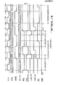
responder 12 may transmit a corresponding acknowledge signal. Since the request signal is less than two clock cycles in duration, a new request may be initiated at the end of every two clock cycles. Similarly, the duration of the acknowledge signal assures its detection at C3 and allows it to repeat every two clock cycles. Therefore, one handshake cycle and data exchange can be completed in the span of two clock cycles, and the obtainable handshake rate as well as data rate are twice that of the known technique illustrated in FIG. 2A for the same system clock rate. - FIGS. 3 and 5 illustrate preferred embodiments of the respective circuits for initiating and acknowledging requests for data exchange. FIGS. 4 and 6 are timing diagrams of various signals in the circuits of FIGS. 3 and 5, respectively. It should be noted that the cross-hatched areas of the signal waveforms indicate that the logic level in those areas is unimportant and thus is labeled "DON'T CARE."
- The
circuit 10 of Fig. 3 for initiating a request, or shortly initiating station, may be divided into three sections. Thefirst section 31 determines whether a request signal RQ should be generated. If an RQ signal is to be generated, thesecond section 33 will provide proper timing for the RQ signal. Thethird section 35 monitors the handshake status. -
Section 31 is preferably implemented by combinational logic comprising ANDgates gate 28, as contained in a commercially available 74F64 integrated circuit package.Section 33 of the preferred embodiment has two D flip-flops conventional delay line 34 and an ANDgate 36.Section 35 has aJK flip flop 38, type 74F109. - Now examples of the operation of
circuit 10 of Fig. 3 will be described with reference to the timing diagram of Fig. 4. -
Section 31 receives the ready to request signal RTR online 45, the acknowledge signal AK online 51 and a DONE signal online 60 from the JK flip-flop 38. The DONE signal is generated by the flip-flop 38 when a handshake cycle is completed, as it will be described in more detail below. Test command signals STOP-HS and FORCE-HS may also be supplied vialines section 31 from the system controller for testing purposes. The STOP-HS signal, when in an active high state, completely inhibits generation of' request signals. The FORCE-HS signal is active in its low state, it overrides the STOP-HS signal and forces generation of a request signal regardless of the status of any other control signal. - The status of the above-described input signals is examined by the
section 31 and a request enabling signal RQ-GO is provided onoutput line 63 therefrom in the following situations. - First, if the previous handshake is completed and both the DONE signal from flip-
flop 38 and the ready to request signal RTR are in their active low states, a normal handshake is initiated. The second situation is that of an overlapped handshake when both the RTR signal and the acknowledge signal AK are in their active low states, regardless of the state of the DONE signal. The third situation involves testing by the system controller. If the forced handshake signal FORCE-HS online 62 is in its active low state, the request go signal RQ-GO online 63 assumes its active high condition. The STOP-HS signal online 61 causes the RQ-GO signal to go low and thus inhibits generation of a request signal RQ by thesection 33. The forced handshake signal FORCE-HS overrides the STOP-HS signal, as previously indicated. - The
second section 33 of the initiator circuit generates the request signal RQ online 50 with the proper timing and duration. Both flip-flops flop 30 is connected to the D input of the second flip-flop 32 vialine 64. At the first clock rising edge after the RQ-GO signal online 63 goes to its active high state, flip-flop 30 is set and its Q output online 64 goes high. Its complementary outputQ goes low and thus provides an active low RU output signal online 50. - The Q output signal from the flip-
flop 30 also is connected to the set input terminal thereof. This arrangement assures that the flip-flop 30 will not change state at the rising edge of the clock pulse immediately following the pulse which sets it. Therefore, the request signal RQ will be greater than one clock cycle in duration. - The second rising edge of the clock signal CLK after the RQ-GO signal goes high will set the flip-
flop 32 causing its Q output to assume a high signal level and its Q output connected to line 65 to go low. Because of the presence of a non-active high reset signal RST online 47, after a short delay To of less than one clock cycle, for example one half of a clock cycle introduced by thedelay line 34, the Q output signal from the flip-flop 32 will clear via ANDgate 36 andline 66 both flip-flops - It is seen from the timing diagram of FIG. 4 that the delayed
signal line 66 which resets the flip-flops delay line 34. Because the transition of a particular request signal RQ(N) from a low active state back to a high non-active state occurs between two consecutive clock edges, the clock edge following that transition may be utilized for generation of a subsequent request signal RQ (N+l) if an acknowledge signal AK (N) in response to the request signal RQ(N) has been generated. That subsequent request signal RQ(N+1) overlaps in time with the acknowledge signal AK(N) thereby overlapping handshakes (N) and (N+I) as it is seen in the example of FIG. 4. - The
third section 35 of the initiator comprising the JK flip-flop 38 is continuously clocked by the clock signal CLK at the rising edge of each clock pulse. It receives the request signal RQ online 64 at its J input terminal and the acknowledge signal AK at its K input and it monitors the handshake status. Each generated request signal RQ online 50 causes the Q output terminal of flip-flop 38 go high, that is to assume the "not done" state online 60, until a responding acknowledge signal AK is received. When an active low AK signal is received online 51, the flip-flop 38 is reset. Its Q output terminal goes low, and the DONE signal online 60 assumes its active low or "done" state indicating that a handshake cycle has been completed. The flip-flop 38 also may be reset to the "done" state by the reset signal RST online 47. - A truth table depicting the above-described operation of the flip-
flop 38 of Fig. 3 is shown in TAB. 1:
- With further reference to FIG. 4, a normal handshake cycle is shown during clock cycles Cl and C2 from the beginning of request (N) to the beginning of request (N+1). During that cycle and acknowledge (N) in response to the request (N) starts at clock C2 and it overlaps a next consecutive request (N+l) during the first half of clock cycle C3.
- In absence of a wait condition, an acknowledge (N+1) would normally start at the positive going edge of clock C4. However, when a wait condition occurs, as it is for example shown at C4, the AK signal remains in its non-active high state past the next clock edge C5. Consequently, the RQ-GO signal is low at clock C5, indicating that the
AK signal online 51 has not been received by the he circuit of FIG. 3. When thereafter an AK signal is received at the next clock C6, a next request (N+2) could be normally generated. However, the Ready to request signal RTR at clock C6 is in its non-active high state and therefore the RQ-GO signal is also in its non-active low state. Consequently, a subsequent request signal RQ cannot be generated until the RTR signal returns to its active low level. - It will be appreciated that the data to be exchanged may be placed on the data bus and accepted from the
data bus 44 in a variety of ways in response to the signals available in theinitiator 10 logic. For example, as is illustrated in FIG. 3, conventional data transmit and data receiveregisters station 10 and thedata bus 44. Data to be transmitted from theinitiator station 10 may be applied to the data transmitregister 40 and clocked into that register by the request signal RQ online 64 from the Q output terminal of the flip-flop 30. Thereafter, that data may be applied fromregister 40 to thedata bus 44. Similarly, the DONE signal from the Q output terminal of flip-flop 38 may be used to clock data from the data bus into the data receiveregister 42 so that data is available from the output of the register for further processing. - A preferred embodiment of the logic circuitry of the
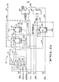
responder 12 for acknowledging a request is illustrated in FIG. 5. FIG. 6 shows timing of various signals in the circuit of FIG. 5. It is seen from a comparison of FIGS. 3 and 5 that the circuit elements implementing the initiating and the respondingstations - In the
responder circuit 12 of Fig. 5,section 31 determines whether conditions necessary for generating an acknowledge signal AK online 51 are met.Section 33 provides proper timing for the AK signal.Section 35 comprising flip-flop 38 monitors whether there is a pending acknowledgement signal. - FIG. 6 generally illustrates the logic levels and timing relationships of the various signals applied to and produced by the circuit of FIG. 5.
- With further reference to FIGS. 5 and 6,
section 31 of theresponder circuit 12 receives a ready to acknowledge signal RTA online 46. A request signal RQ, for example from theinitiator 10 shown in FIG. 3 is received online 50. The output signal online 51 from the Q terminal of flip-flop 30 in FIG. 5 is an acknowledge signal AK, generated by theresponder 12. - The reset signal RST on
line 47 is connected to the set terminal of flip-flop 38 rather than to its clear terminal, as it has been the case in FIG. 3. The output signal from the Q terminal of flip-flop 38 online 70 of Fig. 5 is an AK-PENDING signal. It is in its active low state when an acknowledgement signal AK is pending. The flip-flop 38 is initialized by the RST signal to obtain a non-active high state of the AK-PENDING signal online 70, indicating that generation of an acknowledge signal AK by the circuit of FIG. 5 is not pending. When an RQ signal online 50 is received, the AK-PENDING signal online 70 will be in its active low pending state. In case an AK signal is pending, a next succeeding request signal RQ cannot be generated until flip-flop 38 is reset by the AK signal online 74 and the AK-PENDING signal online 70 becomes active low. - FIG. 6 shows a wait condition as being introduced at clock C3 in response to a "not ready" high status of the ready to acknowledge signal RTA. Consequently, the AK-GO signal is at its non-active low state and an acknowledge (N+l) in response to request (N+l) cannot be generated at clock C3. At the next consecutive clock C4 the RTA signal is again high, AK-GO is low and therefore AK cannot be generated. At the following consecutive clock C5 the RTA signal is active low, the AK-GO signal is active high and a
AK signal (N+l) corresponding to the request (N+1) is generated. It is seen from FIG. 6 that the acknowledge (N+l) has been delayed by two clock cycles C3 and C4 due to the wait condition. - Thus a delayed acknowledged signal AK is generated on
line 51 by the circuit of FIG. 6 when the RTA signal applied to thegate 24 is active low and there is an acknowledgement pending, that is theJ-K flip flop 38 is reset and the ACK-PENDING signal online 70 is active low. The signal AK is generated for an immediate acknowledgement that is without delay when if the RTA signal is active low and the request signal RQ is at its active low state. As with the initiator, the circuit test mode is operative when the FORCE-HS signal is at its active low state forcing the generation of the acknowledgement signalAK. - The truth table depicting the operation of the flip-
flop 38 of Fig. 5 is shown in TAB. 2 below:
- The principles, preferred embodiments and modes of operation of the present invention have been described in the foregoing specification. The invention which is intended to be protected herein, however, is not to be construed as limited to the particular embodiments disclosed, since these are to be regarded as illustrative rather than restrictive. Moreover, variations and changes may be made by those skilled in the art without departing from the scope of the present invention.
Claims (19)
Applications Claiming Priority (2)
| Application Number | Priority Date | Filing Date | Title |
|---|---|---|---|
| US809699 | 1985-12-17 | ||
| US06/809,699 US4727370A (en) | 1985-12-17 | 1985-12-17 | Method and system for synchronous handshake generation |
Publications (2)
| Publication Number | Publication Date |
|---|---|
| EP0228811A2 true EP0228811A2 (en) | 1987-07-15 |
| EP0228811A3 EP0228811A3 (en) | 1989-09-27 |
Family
ID=25202020
Family Applications (1)
| Application Number | Title | Priority Date | Filing Date |
|---|---|---|---|
| EP86309185A Withdrawn EP0228811A3 (en) | 1985-12-17 | 1986-11-25 | Method and system for synchronous handshake generation |
Country Status (4)
| Country | Link |
|---|---|
| US (1) | US4727370A (en) |
| EP (1) | EP0228811A3 (en) |
| JP (1) | JPS62155651A (en) |
| IL (1) | IL79989A0 (en) |
Cited By (5)
| Publication number | Priority date | Publication date | Assignee | Title |
|---|---|---|---|---|
| EP0288191A2 (en) * | 1987-04-20 | 1988-10-26 | Tandem Computers Incorporated | Method and apparatus for data transfer handshake pipelining |
| EP0347557A2 (en) * | 1988-06-24 | 1989-12-27 | International Business Machines Corporation | Dual clocked data bus |
| US5081701A (en) * | 1987-04-20 | 1992-01-14 | Tandem Computers Incorporated | System for controlling data transfer using transfer handshake protocol using transfer complete and transfer inhibit signals |
| EP0805400A1 (en) * | 1990-07-03 | 1997-11-05 | National Instruments Corporation | IEEE488 interface and message handling method |
| EP2026493A1 (en) * | 2007-08-16 | 2009-02-18 | STMicroelectronics S.r.l. | Method and systems for mesochronous communications in multiple clock domains and corresponding computer program product |
Families Citing this family (21)
| Publication number | Priority date | Publication date | Assignee | Title |
|---|---|---|---|---|
| US4926448A (en) * | 1986-05-06 | 1990-05-15 | Hayes Microcomputer Products, Inc. | Method and apparatus for implementing an escape sequence |
| DK155265C (en) * | 1986-06-09 | 1989-07-31 | Rovsing As Christian | PROCEDURE FOR CONNECTING A DATA UNIT ON A SIGNAL PIPE AND APPARATUS FOR EXERCISING THE PROCEDURE |
| US4995785A (en) * | 1986-09-12 | 1991-02-26 | Kornelis Platteschorre | Egg carton stacking-loading device and method |
| US4807258A (en) * | 1987-11-17 | 1989-02-21 | Gte Laboratories Incorporated | Method for synchronizing a digital communication system |
| US4931250A (en) * | 1988-05-12 | 1990-06-05 | Codex Corporation | Multimode modem |
| WO1990003701A1 (en) * | 1988-09-27 | 1990-04-05 | Texas Instruments Japan Ltd. | Method of matching operation mode of a modem |
| US4910754A (en) * | 1988-09-30 | 1990-03-20 | Data General Corporation | Initialization and synchronization method for a two-way communication link |
| US5020081A (en) * | 1988-09-30 | 1991-05-28 | Data General Corporation | Communication link interface with different clock rate tolerance |
| US4941157A (en) * | 1989-04-14 | 1990-07-10 | Ncr Corporation | Slow peripheral handshake interface circuit |
| US5155746A (en) * | 1990-01-08 | 1992-10-13 | Reliance Comm/Tec Corporation | Clock synchronization scheme for digital transmission |
| US5493609A (en) * | 1990-09-27 | 1996-02-20 | Radish Communications Systems, Inc. | Telecommunication system for automatic switching between voice and data communications |
| GB2262415B (en) * | 1991-12-13 | 1995-08-16 | Digital Equipment Int | Handshake synchronization system |
| US6581126B1 (en) * | 1996-12-20 | 2003-06-17 | Plx Technology, Inc. | Method, system and apparatus for a computer subsystem interconnection using a chain of bus repeaters |
| JP3161420B2 (en) * | 1998-07-30 | 2001-04-25 | 日本電気株式会社 | Asynchronous interface system |
| US6247082B1 (en) * | 1998-11-03 | 2001-06-12 | 3Com Corporation | Method and circuit for providing handshaking to transact information across multiple clock domains |
| US7058973B1 (en) * | 2000-03-03 | 2006-06-06 | Symantec Corporation | Network address translation gateway for local area networks using local IP addresses and non-translatable port addresses |
| US6801936B1 (en) * | 2000-04-07 | 2004-10-05 | Arif Diwan | Systems and methods for generating customized bundles of information |
| DE10130797A1 (en) * | 2001-06-26 | 2003-01-02 | Infineon Technologies Ag | Interface for data transmission |
| US7065602B2 (en) * | 2003-07-01 | 2006-06-20 | International Business Machines Corporation | Circuit and method for pipelined insertion |
| US9110771B2 (en) | 2008-06-13 | 2015-08-18 | New York University | Computations using a polychronous wave propagation system |
| CN109960672B (en) * | 2017-12-22 | 2022-12-30 | 苏州迈瑞微电子有限公司 | Digital communication method based on GPIO interface |
Family Cites Families (7)
| Publication number | Priority date | Publication date | Assignee | Title |
|---|---|---|---|---|
| GB1463626A (en) * | 1974-05-01 | 1977-02-02 | Solartron Electronic Group | Data transmission system |
| US3866172A (en) * | 1974-05-16 | 1975-02-11 | Bell Telephone Labor Inc | Communication system for transmitting data words prior to receipt of acknowledgments for previously transmitted data words |
| JPS5931274B2 (en) * | 1979-06-05 | 1984-08-01 | 岩崎通信機株式会社 | Synchronization method in button telephone equipment |
| GB2075310A (en) * | 1980-04-30 | 1981-11-11 | Hewlett Packard Ltd | Bus extender circuitry for data transmission |
| US4390967A (en) * | 1980-10-14 | 1983-06-28 | Interface Systems, Inc. | Interface system wherein the interface is addressed before data transfer from a selected device |
| JPS57189231A (en) * | 1981-05-18 | 1982-11-20 | Advantest Corp | Data transferring system |
| US4475191A (en) * | 1982-12-10 | 1984-10-02 | At&T Bell Laboratories | Distributed time division multiplexing bus |
-
1985
- 1985-12-17 US US06/809,699 patent/US4727370A/en not_active Expired - Lifetime
-
1986
- 1986-09-09 IL IL79989A patent/IL79989A0/en not_active IP Right Cessation
- 1986-11-25 EP EP86309185A patent/EP0228811A3/en not_active Withdrawn
- 1986-12-17 JP JP61301108A patent/JPS62155651A/en active Pending
Non-Patent Citations (1)
| Title |
|---|
| ELECTRO AND MINI/MICRO NORTHEAST, New York, 23rd-25th April 1985, session 8/3, pages 1-9, New York, US; S.D. COOPER: "Multibusr II - A major advancement in multiprocessing" * |
Cited By (9)
| Publication number | Priority date | Publication date | Assignee | Title |
|---|---|---|---|---|
| EP0288191A2 (en) * | 1987-04-20 | 1988-10-26 | Tandem Computers Incorporated | Method and apparatus for data transfer handshake pipelining |
| EP0288191A3 (en) * | 1987-04-20 | 1990-07-04 | Tandem Computers Incorporated | Method and apparatus for data transfer handshake pipelining |
| AU608595B2 (en) * | 1987-04-20 | 1991-04-11 | Tandem Computers Incorporated | Method and apparatus for data transfer handshake pipeline |
| US5081701A (en) * | 1987-04-20 | 1992-01-14 | Tandem Computers Incorporated | System for controlling data transfer using transfer handshake protocol using transfer complete and transfer inhibit signals |
| EP0347557A2 (en) * | 1988-06-24 | 1989-12-27 | International Business Machines Corporation | Dual clocked data bus |
| EP0347557A3 (en) * | 1988-06-24 | 1991-06-05 | International Business Machines Corporation | Dual clocked data bus |
| EP0805400A1 (en) * | 1990-07-03 | 1997-11-05 | National Instruments Corporation | IEEE488 interface and message handling method |
| EP2026493A1 (en) * | 2007-08-16 | 2009-02-18 | STMicroelectronics S.r.l. | Method and systems for mesochronous communications in multiple clock domains and corresponding computer program product |
| US7925803B2 (en) | 2007-08-16 | 2011-04-12 | Stmicroelectronics S.R.L. | Method and systems for mesochronous communications in multiple clock domains and corresponding computer program product |
Also Published As
| Publication number | Publication date |
|---|---|
| EP0228811A3 (en) | 1989-09-27 |
| JPS62155651A (en) | 1987-07-10 |
| US4727370A (en) | 1988-02-23 |
| IL79989A0 (en) | 1986-12-31 |
Similar Documents
| Publication | Publication Date | Title |
|---|---|---|
| US4727370A (en) | Method and system for synchronous handshake generation | |
| US3988716A (en) | Computer interface system | |
| US4050097A (en) | Synchronization technique for data transfers over an asynchronous common bus network coupling data processing apparatus | |
| US5600824A (en) | Clock generating means for generating bus clock and chip clock synchronously having frequency ratio of N-1/N responsive to synchronization signal for inhibiting data transfer | |
| US4390969A (en) | Asynchronous data transmission system with state variable memory and handshaking protocol circuits | |
| US5179670A (en) | Slot determination mechanism using pulse counting | |
| US4450572A (en) | Interface for serial data communications link | |
| US4785396A (en) | Push-pull serial bus coupled to a plurality of devices each having collision detection circuit and arbitration circuit | |
| JPH03191633A (en) | Data transfer system | |
| US5128666A (en) | Protocol and apparatus for a control link between a control unit and several devices | |
| US5418825A (en) | Time-domain boundary bridge method and apparatus | |
| US4040014A (en) | Modem sharing device | |
| US4468737A (en) | Circuit for extending a multiplexed address and data bus to distant peripheral devices | |
| CA1322034C (en) | Bidirectional control signalling bus interface apparatus for transmitting signals between two bus systems | |
| US6295300B1 (en) | Circuit and method for symmetric asynchronous interface | |
| KR950008661B1 (en) | Bus multiplexing apparatus | |
| US6651127B2 (en) | Method of detecting termination of a bus transfer operation | |
| EP0357413B1 (en) | Data transfer control circuit | |
| US6016521A (en) | Communication control device | |
| US6246726B1 (en) | High speed digital data transmission by separately clocking and recombining interleaved data subgroups | |
| KR0146058B1 (en) | Priority arbitrating apparatus | |
| EP1242897B1 (en) | Method and apparatus for differential strobing in a communications bus | |
| JPS6361349A (en) | Interface control system | |
| JPS63103531A (en) | Relay control system for digital signal | |
| KR950006826Y1 (en) | Serial data transmission circuit |
Legal Events
| Date | Code | Title | Description |
|---|---|---|---|
| PUAI | Public reference made under article 153(3) epc to a published international application that has entered the european phase |
Free format text: ORIGINAL CODE: 0009012 |
|
| AK | Designated contracting states |
Kind code of ref document: A2 Designated state(s): CH DE FR GB IT LI NL SE |
|
| PUAL | Search report despatched |
Free format text: ORIGINAL CODE: 0009013 |
|
| AK | Designated contracting states |
Kind code of ref document: A3 Designated state(s): CH DE FR GB IT LI NL SE |
|
| 17P | Request for examination filed |
Effective date: 19891221 |
|
| 17Q | First examination report despatched |
Effective date: 19920731 |
|
| RAP1 | Party data changed (applicant data changed or rights of an application transferred) |
Owner name: AMPEX SYSTEMS CORPORATION |
|
| STAA | Information on the status of an ep patent application or granted ep patent |
Free format text: STATUS: THE APPLICATION HAS BEEN WITHDRAWN |
|
| 18W | Application withdrawn |
Withdrawal date: 19940101 |
|
| RAP1 | Party data changed (applicant data changed or rights of an application transferred) |
Owner name: AMPEX CORPORATION |
|
| RIN1 | Information on inventor provided before grant (corrected) |
Inventor name: SHIH, LIONEL C. |