EP0230746A2 - Jack device - Google Patents
Jack device Download PDFInfo
- Publication number
- EP0230746A2 EP0230746A2 EP86309708A EP86309708A EP0230746A2 EP 0230746 A2 EP0230746 A2 EP 0230746A2 EP 86309708 A EP86309708 A EP 86309708A EP 86309708 A EP86309708 A EP 86309708A EP 0230746 A2 EP0230746 A2 EP 0230746A2
- Authority
- EP
- European Patent Office
- Prior art keywords
- signal
- housing
- coaxial cable
- conducting
- conductor
- Prior art date
- Legal status (The legal status is an assumption and is not a legal conclusion. Google has not performed a legal analysis and makes no representation as to the accuracy of the status listed.)
- Granted
Links
Images


Classifications
-
- H—ELECTRICITY
- H01—ELECTRIC ELEMENTS
- H01R—ELECTRICALLY-CONDUCTIVE CONNECTIONS; STRUCTURAL ASSOCIATIONS OF A PLURALITY OF MUTUALLY-INSULATED ELECTRICAL CONNECTING ELEMENTS; COUPLING DEVICES; CURRENT COLLECTORS
- H01R24/00—Two-part coupling devices, or either of their cooperating parts, characterised by their overall structure
- H01R24/38—Two-part coupling devices, or either of their cooperating parts, characterised by their overall structure having concentrically or coaxially arranged contacts
- H01R24/40—Two-part coupling devices, or either of their cooperating parts, characterised by their overall structure having concentrically or coaxially arranged contacts specially adapted for high frequency
- H01R24/42—Two-part coupling devices, or either of their cooperating parts, characterised by their overall structure having concentrically or coaxially arranged contacts specially adapted for high frequency comprising impedance matching means or electrical components, e.g. filters or switches
- H01R24/46—Two-part coupling devices, or either of their cooperating parts, characterised by their overall structure having concentrically or coaxially arranged contacts specially adapted for high frequency comprising impedance matching means or electrical components, e.g. filters or switches comprising switches
-
- H—ELECTRICITY
- H01—ELECTRIC ELEMENTS
- H01R—ELECTRICALLY-CONDUCTIVE CONNECTIONS; STRUCTURAL ASSOCIATIONS OF A PLURALITY OF MUTUALLY-INSULATED ELECTRICAL CONNECTING ELEMENTS; COUPLING DEVICES; CURRENT COLLECTORS
- H01R13/00—Details of coupling devices of the kinds covered by groups H01R12/70 or H01R24/00 - H01R33/00
- H01R13/66—Structural association with built-in electrical component
- H01R13/70—Structural association with built-in electrical component with built-in switch
- H01R13/703—Structural association with built-in electrical component with built-in switch operated by engagement or disengagement of coupling parts, e.g. dual-continuity coupling part
-
- H—ELECTRICITY
- H01—ELECTRIC ELEMENTS
- H01R—ELECTRICALLY-CONDUCTIVE CONNECTIONS; STRUCTURAL ASSOCIATIONS OF A PLURALITY OF MUTUALLY-INSULATED ELECTRICAL CONNECTING ELEMENTS; COUPLING DEVICES; CURRENT COLLECTORS
- H01R2103/00—Two poles
Definitions
- the present invention is directed to electrical equipment, and more particularly to jack assemblies for connecting two or more cables together for use, for example, in the telecommunications or broadcast industries.
- Transmission networks for analog signals, digital voice or digital data information are comprised increasingly of a complex interconnecting array of many types of equipment. Because the networks tend to be large and routed complexly, the various types of equipment provide for managability, test, maintenance, reconfiguration, and growth. Typically, a set of equipment is located in each of a number of facilities, such as telephone switching offices. The various facilities are interconnected in any of a variety of ways including coaxial cable, microwave, satellites, etc.
- a crucial capability for any set of equipment in a transmission network is the ability to cross connect one piece of equipment to another. Such ability accommodates particularly maintenance, reconfiguration and test functions.
- Cross connection is accomplished by receiving a plug or other termination mechanism from one cable or other carrier and connecting in a suitable fashion to another plug or termination mechanism of another cable or carrier.
- the cross connection device may include additional access, such as for monitoring or testing.
- Cross connect jack devices are known.
- Known devices however, have a limited frequency range and limited versatility with respect to configuring for different situations.
- the present invention is directed to these and other novel features.
- the present invention is directed to a jack device for cross connecting a first coaxial cable with one of second and third coaxial cables.
- the jack device includes a housing, a mechanism for conducting an electrical signal through the housing, and a mechanism for supporting the conducting mechanism with respect to the housing.
- the housing includes a grounding mechanism for connecting between the coaxial cables.
- the conducting mechanism includes a mechanism for switching a signal from passing between the first and second coaxial cables to passing between the first and third coaxial cables, while at the same time having a characteristic impedance having approximately equal inductive and capacitive reactive components.
- a prime operating parameter is the matching of impedances of the equipments.
- Impedance has capacitive, inductive and resistive components. Capacitive and inductive components work to cancel one another.
- the present invention comprises a jack device having a characteristic impedance which advantageously includes approximately equal inductive and capacitive reactances. In this way, the induced capacitance as a result of the capacitor-like surfaces inherent in a switching mechanism are essentially neutralized.
- the switching mechanism of the present invention is a unique make-before-break type.
- a spring conductor having opposite first end portions connected to a first central portion by first cantilever portions is held by a holding mechanism at the first central portion to the shells of the housing.
- a somewhat similar lever conductor having second end portions connected to a second central portion by second cantilever portions is also held by the holding mechanism. The first and second central portions are spaced apart.
- the first cantilever portion is moved so that the appropriate first end portion of the spring conductor wipes along a conductor now in continuity with the plug and breaks contact from it.
- the switch advantageously is formed to provide a wiping action at each of the contacting surfaces.
- the second central portion is connected through a resistor to the housing thereby providing a load to ground for the circuit which is disconnected.
- the jack device in another embodiment, includes a housing for connecting a first coaxial cable with a second coaxial cable.
- the housing includes a passageway therethrough and mechanism for maintaining a ground connection between the cables.
- the jack device of this embodiment further includes conducting mechanism having an elongated connector member and mechanism for supporting the conducting member with respect to the housing.
- the supporting mechanism includes a dielectric support member having regularly spaced cavities about the conductor member. In this way the support member has a characteristic impedance which is approximately equal to the characteristic impedance of the first and second coaxial cables.
- the characteristic impedance may be made approximately the same as the characteristic impedance of the cables.
- the present invention thus, not only provides for equalizing capacitive and inductive reactances, but also for supporting the conductive members such that the impedances of the supports are approximately the same as the impedance of the cables.
- Yet another embodiment of the jack device of the present invention cross connects at least one input cable with at least one output cable and includes a housing, conducting mechanism and mechanism for supporting the conducting mechanism.
- the housing has front and rear modules. Each of the modules includes mechanism for receiving at least one of the termination means of the cables.
- the housing further includes a pair of shells for fitting about portions of the modules to hold the modules together.
- the indicated housing is particularly advantageous because of it modular approach.
- the front module may have either one or two sleeves for receiving plugs.
- the sleeves may be of different diameters.
- the rear module may be formed with various types of mechanisms for receiving the termination means of a particular cable. For example, it may include one or two of any of a sleeve for receiving a bayonet connector, a sleeve for receiving a threaded connector, or a sleeve which may be crimped onto the coaxial or other cable. As a result, numerous configurational combinations may be created.
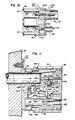
- a jack device in accordance with the present invention is designated generally as 20.
- Device 20 is attached to panel 22 with a screw 23 (see FIGURE ll) passing through opening 24 and threading into a hole in panel 22.
- Jack device 20 incluvers a housing 26, a conducting mechanism 28, and mechanism 30 for supporting conducting mechanism 28 with respect to housing 26 (see FIGURE 2).
- jack device 20 may include a mechanism 32 for monitoring the signal passing through device 20.
- Monitoring mechanism 32 includes a signal conducting cable 34 extending to, for example, a connecting jack 36 shown mounted to panel 22.
- Housing 26 includes front and rear modules 38 and 40, respectively.
- Modules 38 and 40 have mating first ends 42 and 44 and opposing second ends 46 and 48.
- One or more sleeves 50 extend outwardly from the second end 46 of front module 38.
- a front module 38 having a single sleeve is shown in FIGURE 7, while a front module 38 having two sleeves 50 is shown in FIGURE 8.
- Sleeves 50 are formed to receive a con necting plug from a coaxial cable as shown, for example, in FIGURE l at 52.
- Connecting sleeves 54 are attached to second end 48 of rear module 40.
- Jack device 20 is intended to have two sleeves 54 attached to rear module 40, but as shown in FIGURES 9 and l0, the sleeves may assume various forms.
- FIGURE 9 shows a conventional bayonet connector receiving sleeve 56 and a crimp sleeve 58 wherein the center conductor of a coaxial cable is attached to conductor l57 fastened in rear module 40.
- Sleeve 58 is crimped so as to make contact with and hold the shield of the cable.
- l0 connecting sleeve 54 is shown in the form of a threaded sleeve 60 for receiving a standard threaded connector, and is also shown in the form of a larger crimp sleeve 58′.
- Front and rear modules 38 and 40 are held together by a pair of opposing shells 62 which are attached together with a pair of nut and bolt assemblies 64 as shown in FIGURE l.
- Front and rear modules 38 and 40, as well as sleeves 50 and connecting sleeves 54 are preferably conductive.
- front module 38 is formed as two parallel cylinders 66 held together in the parallel configuration by forward and rearward transverse bulkheads 68 and 70.
- Each cylinder 66 is formed to have an essentially cylindrical passageway 72 therethrough which is axially aligned with any sleeve 50 extending from front bulkhead 68 on the side opposite cylinder 66.
- the rearward portion of passageway 72 is inclined in a frusto-conical shape to expand toward the rear.
- each cylinder wall includes a pair of openings 74.
- the inclined wall of passageway 72 includes a plurality of regularly spaced grooves 76 (see FIGURE 5).
- groove 76 running axially and aligned with each opening 74. Grooves 76 are needed to receive protuberances 272 on support members 252 during assembly.
- the support members 252 fit into passageways 72 until the inclined side wall of support member 252 mates with the inclined wall of passageway 72 and the protuberances 272 fit into openings 74 to snugly hold the support member 252 in the end of passageway 72.
- cylinders 66 are formed as half cylinders with only the opposing halves present. The enlarged empty region 78 is then available for switch mechanism l56 as discussed hereinafter.
- Each cylinder 66 also includes a short recess portion 80 at the rearward end in order to fit into a mating recess ll4 in the forward bulkhead 98 of rear module 40.
- Another recess portion 82 is formed in the outer sidewall of cylinders 66 just rearward of forward bulkhead 68.
- Recess portion 82 extends along almost half the distance between forward and rearward bulkheads 68 and 70.
- Relatively large rectangular openings 84 are formed in the recess portions 82 of each cylinder 66 and are centered on the horizontal cross sectional plane of the jack device 20.
- Recess portion 82 is formed to receive ground spring 86.
- Ground spring 86 has end portions 88 (see FIGURE l) which wrap around the cylinders 66.
- Each end portion 88 includes a detent 90 which protrudes through an opening 84.
- detent 90 When a plug 52 is inserted into sleeve 50, the outer surface of plug 52 contacts detent 90 and forces end portion 86 outwardly so that a spring force is maintained at the contact between ground spring 86 and the plug 52.
- the center portion 92 of ground spring 86 extends between the end portions 88 and is fastened in place with one of nut and bolt combinations 64. Centered at the forward end of ground spring 86 is a tab 94 (see FIGURE 6) which is bent inwardly for the purpose of contacting a resistor l74 as discussed hereinafter.
- Rear module 40 also includes a pair of parallel cylinders 96 held in the parallel configuration by a forward bulkhead 98 and a rearward connecting segment l00.
- Connecting segment l00 includes a pair of spaced apart ridges l02 and l04 running transversely about rear module 40. Ridges l02 and l04 have the general shape of forward bulkhead 98 and function in combination with it to longitudinally retain rear module 40 to shells 62.
- Cylinders 96 have cylindrical passageways l06 extending therethrough and being axially aligned with passageways 72 of forward module 38. The rearward ends of passageways l06 are larger than the rest of passageways l06 and have an inclined frusto-conical wall l08 expanding toward the rearward end.
- wall l08 has a plurality of regularly spaced axially running grooves ll0 (see FIGURE 3).
- a pair of openings ll2 pass through the walls of each cylinder 96 and are aligned with a pair of grooves ll0.
- Support member 250 includes a protuberance 264 which slides along grooves ll0 during installation.
- the outer side surface of support member 250 is frusto-conically shaped and mates with wall l08 at the point when the protuberances 264 enter into openings ll2 to retain support member 250 in place.
- Forward bulkhead 98 of rear module 40 has a recess ll4 in end 44 to receive end 42 of forward module 38.
- the outer perimeter of bulkhead 98 fits about recess 80 of module 38 while the end 42 of module 38 fits into recess ll4 of rear module 40.
- the rear end 48 of rear module 40 has sleeve-like flanges ll6 extending as projections of cylinders 96.
- Flanges ll6 have thinner walls than the ends of cylinders 96 at the end of passageways l08 so that there is a circular shoulder ll8 against which the end flanges l20 of connecting sleeves 54 butt.
- Flanges ll6 are bent over flanges l20 to retain connecting sleeves 54 to rear module 40.
- FIGURES l and l2 As shown in FIGURES l and l2, about the upper, inner one-third of the cylindrical wall of cylinders 96 is missing to present an open area between forward bulkhead 98 and the forward wall l22 of connecting portion l00.
- the remainder of the facing walls of cylinders 96 have flat vertical surfaces l24 as shown in FIGURE l2.
- the end of surfaces l24 includes an inward projection l26 for the purpose of retaining insulating holder l28 for monitoring components as described hereinafter.
- shells 62 Each shell 62 is identical. As shown in FIGURE 2, shell 62 includes grooves l30, l32 and l34. Rear bulkhead 70 of forward module 38 fits in groove l30. Forward bulkhead 68 butts against the forward end l36 of shell 62. In this way, front module 38 is prevented from moving longitudinally with respect to shells 62.
- Front bulkhead 98 of rear module 40 fits in groove l32. Ridges l02 and l04 fit in wider groove l34. Bulkhead 98 and ridges l02 and l04 in grooves l32 and l34 retain rear module 40 against longitudinal movement with respect to shell 62.
- Shell 62 also includes front and rear posts l38 and l40, respectively.
- Front post l38 includes a forward extending portion l42 for fitting between cylinders 66 of module 38.
- Front post l38 also includes a rear groove l44 for receiving insulating holding members 200 of switch mechanism l56 as discussed hereinafter.
- Rear post l40 includes a forward tongue l46 for fitting into the rear end of holding members 200. Forward and rear posts l38 and l40 extend inwardly sufficiently far so that they butt against one another when upper and lower shells 62 are fastened together.
- FIGURE l3 An electrical schematic of jack device 20 is shown in FIGURE l3.
- a signal is input at connecting end l48 of conductor l49 which is also connected to inductor l5l. If a plug has been inserted in connecting end l52, then a signal passes directly through jack device 20 along conductor l50. If no plug has been inserted in either connecting end l52 or l54, then switch mechanism l56 directs the signal to conductor l58 for output through inductor l59 and conductor l57 at connecting end l60.
- jack device 20 If jack device 20 is used as a pass through connector, then a signal cannot only be input at connecting end l48 and passed through to connecting end l52, but also another signal may be input at connecting end l60 and passed through to connecting end l54. In that case, switch mechanism l56 would be disconnected from both conducting paths.
- end portion l62 of spring conductor l64 is forced against conductor l50 and directs the signal through conductor l64 to opposite end portion l66 which is likewise forced against conductor l58. If a plug is inserted in connecting end l52 as discussed hereinafter lever conductor l68 moves end portion l62 of spring conductor l64 away from conductor l50. Lever conductor l68 similarly moves end portion l66 from conductor l58 if a plug is inserted in connecting end l54.
- lever conductor l68 moves end portion l62 away from conductor l50, the circuit which includes connecting end l60, inductor l59, conductor l58, end portion l66 and switching conductor l64 is completed to ground l72 at end portion l70 and lever conductor l68 through resistor l74.
- lever conductor l68 includes end portion l76 which functions to move switching end portion l66 if a plug is inserted in connecting end l54 and is connected to ground l72 through resistor l74.
- Any signal conducted along line l50 may be monitored through resistor l80 via line l82.
- Resistor l82 is connected to inductor l84 via line l86.
- Inductor l84 is grounded at line l88.
- a monitoring line l87 is center tapped to inductor l84 and leads to connecting end l89.
- monitor branch of the circuit shown in FIGURE l3 is optional, as is connecting end l54. Furthermore, there are cases when a simple pass through circuit is all that is appropriate.
- the switch assembly l56 is shown in greater detail in FIGURE ll.
- the switch assembly l56 includes spring conductor l64 and lever conductor l68 as held by a holding assembly l90.
- Spring conductor l64 is an elongated flat sheet having end portions l92 and a central portion l94 with cantilever portions l96 extending therebetween.
- Central portion l94 is held in a pair of aligned, facing arcuate slots l98 in holding members 200 (see FIGURE 6).
- Central portion l94 curves rearwardly so that cantilever portion l96 extends diagonally rearwardly and sidewardly. At the end of cantilever portion l96, it mates with end portion l92 to extend sidewardly and slightly forwardly to forwardly extending arcuate end 202.
- the conductors l50 and l58 are cylindrical at the locations 202 and 204, where the arcuate ends l62 and l66 make contact with them.
- the curvatures of the arcuate ends l62 and l66 are approximately perpendicular to the curvatures of the cylindrical portions 202 and 204.
- Lever conductor l68 also has end portions 206 and a central portion 208 connected together by cantilever portions 2l0.
- a dielectric sleeve 2l2 is formed about a segment of each of the cantilever portions 2l0 to provide a surface against which plug 52 may slide without making electrical contact with lever conductor l68.
- the central portion 208 of lever conductor l68 is curved rearwardly and held by holding members 200 in facing slots 2l4.
- Cantilever portions 2l0 extend rearwardly and slightly sidewardly from central portion 204.
- the end portions 206 are formed arcuately with inward curvatures. It is noted that central portion 208 has upper and lower tabs 2l6.
- tabs 2l6 are located along the centerline of jack device 20 and are bent rearwardly at the top and bottom of central portion 204. One of tabs 2l6 contacts one end of resistor l74 while tab 94 of ground spring 92 contacts the other end of resistor l74.
- Holding members 200 are identical. Each has protrusions 2l8 slightly sidewardly from the centerline of jack device 20 and openings 220 for receiving the protrusions 2l8 of the other holding member 200. The openings are slightly off the centerline in the other direction from protrusions 2l8. As indicated, holding members 200 have facing slots l98 for receiving spring conductor l64 and facing slots 2l4 for receiving lever conductor l68. Slots 2l4 are forwardly of slots l98 and an opening 222 located between the pairs of slots extends completely through the holding members for the purpose of receiving the bolt of bolt and nut combination 64 in order to hold holding members 200 to shells 62.
- holding members 200 include The forward end of holding members 200 incluvers a tongue 224 for fitting in groove l44 of post l38 on shell 62.
- the rearward end of holding members 200 includes a groove 226 for receiving tongue l46 of post l40 of shell 62.
- Holding members 200 also include arms 228 which extend in both sidewardly directions at the rear end of holding members 200.
- a retainer flange 230 extends in the direction of the arm on the other holding member 200. The retainer flanges 228 prevent the end portions 206 of lever conductor l68 from contacting the end portions l92 of spring conductor l64.
- plug 52 When plug 52 is inserted in sleeve 50, the outer surface of plug 52 contacts dielectric sleeve 2l2 and forces the cantilever portion 2l0 of lever conductor l68 inwardly.
- end portion 206 of lever conductor l68 contacts cantilever portion l96 of spring conductor l64, it forces cantilever portion l96 inwardly thereby breaking contact between arcuate end l62 of end portion l92 and cylindrical portion 202 of conductor l50. It is noted that end portion 206 is arcuate and rubs along the inclined cantilever portion l96 thereby wiping and cleaning the contacting surface between the two conductors.
- end portion l92 angles forwardly and applies a spring force on cylindrical portion 202, when the spring force is overcome by lever conductor l68, arcuate end l62 wipes along and cleans the contacting surface between end l62 and cylindrical portion 202.
- FIGURE l3 The monitoring branch of the circuit shown in FIGURE l3, as indicated previously, is an optional feature.
- inductor l84 is shown.
- the conductors l82 and l86 leading to resistor l80 are indicated.
- Support member l28 holds inductor l84 and resistor l80.
- Support member l28 has a substantially rectangular base 232 to fit in the space between the straight walls l24 of cylinders 96 and between forward bulkhead 98 and wall l22 of rear module 40.
- a post 234 rises above base 232 and includes an opening 236 for receiving the bolt of a nut and bolt combination 64. The bottom of base 232 and the top of post 234 contact opposite shells 62.
- Base 232 includes a plurality of either recesses or channels 238 for receiving prongs 240 of an end member 242 connected to the ground wire of cable 34.
- One prong 244 of the plurality of prongs 240 extends through base 232 to provide a terminal for connection with wire l88 from inductor l84.
- jack device 20 is intended to be an interconnecting mechanism for passing a signal from one transmission line to another, a crucial consideration is power transmission through the connecting device.
- a direct current circuit power is reduced at each resistive component.
- an alternating current circuit such as any circuit in which the present jack device 20 would be used, the same is true except for the resistive component one must more generally consider the effects of inductance and capacitance and consequently, the important parameter is impedance.
- any direct current circuit in going from one conductor to another it is important to keep contact resistance low so that the resistance per unit length of the conductors is not increased at the contact, so with an alternating current circuit it is important to match the impedance from one device to another.
- FIGURES l4A and l4B Since impedance is related inversely to frequency, the problem of matching impedance is evermore difficult as frequencies rise.
- FIGURE A In the voltage diagrams in FIGURES l4A and l4B.
- FIGURE l4B A phase diagram of typical component voltages is illustrated in FIGURE l4B.
- a resolution of the voltage as shown in FIGURE l4B is shown in FIGURE l4C.
- the present invention has addressed not only the performance parameter of impedance matching, but has also matched capacitive and inductive reactances so as to keep the voltage and current in phase through the jack device and thereby reduce any reactive power loss.
- the present invention represents a recognition not only of the necessity to match impedances from one conductive component to another throughout the transmission circuit in the jack device, but also of the desirability to equalize inductive and capacitive components of the impedance.
- the end portion l92 of spring conductor l64 in switch mechanism l56 and the cylindrical wall 202 of conductor l50 provides surfaces of a type commonly found in capacitors. Consequently, there is an induced capacitive effect in jack device 20 as a result of the relationship of the switch surfaces.
- an inductor l5l is introduced between conductors l49 and l50.
- inductor l59 is installed between conductors l57 and l58 to provide inductive reactance to counter the capacitive reactance of the other side of spring conductor l64.
- an RG 59 B/U 75 ohm coaxial cable was connected to incoming connecting end l48 and a precision 75 ohm termination device was connected to connecting end l60.
- a time domain reflectometer was then appropriately connected to the coaxial cable.
- the graph of FIGURE l5 showing the impedance characteristics of the circuit was developed. Rises above the straight 75 ohm line are due to inductive reactance, while rises below the line are due to capacitive reactance. It is noted that the present invention resulted in both capacitive and inductive reactances which approximately canceled so as to relatively closely maintain an average 75 ohm impedance through jack device 20.
- jack device 20 When analyzing the distributed effects of geometry to the contributions to impedance, another part of jack device 20 which must be carefully considered are the support structures between the signal carrying conductors and the ground mechanism, preferably the conductive housing of present jack device 20.
- the impedance between a conductor and a coaxial shield depends on the distance between the two items. If a substance other than air is inserted somewhere between the two items, for example, to hold the central conductor with respect to the outer shield, then a dielectric constant somewhat less efficient than air has been introduced and a different impedance results.
- Prior art connectors show solid disk-like support members between a central conductor and an outer conductive housing.
- the present invention is recognition of the possibility of not only varying the distance between the central conductor and the wall of the housing, or varying the substance for the support member thereby varying the dielectric constant, but is also recognition of the advantage which is achievable by using support members of geometries which incorporate both a dielectric material and air cavities between the central conductor and the wall of the conductive housing.
- Conductor l49 is supported by support member 246 with respect to connecting sleeve 54 and is further supported by support member 250 with respect to rear module 40.
- Conductor l50 is supported by support member 252 with respect to front module 38.
- Conductors l57 and l58 in the other cylinders of front and rear modules 38 and 40 are similarly supported.
- Conductor l49 has a connecting end l48 for receiving a straight conductor of a mating plug.
- Conductor l49 also has a knurled portion 254 as well as enlarged ends at the rear end of support member 246 and the front end of support member 250 in order to rigidly retain conductor l49 to support members 246 and 250 and keep the conductors centered with respect to sleeve 54 and cylindrical wall l06.
- conductor l50 has a forward end shaped to receive a straight conductor and has a knurled portion 256 for making good mechanical contact with support member 252 and keeping conductor l50 centered with respect to cylindrical wall 72 and cylindrical wall l06 of front and rear modules 38 and 40.
- support members 246 and 250 are shaped similarly.
- Support member 250 has a central core 258 with an axial opening for receiving and holding conductor l49.
- a plurality of spokes 260 extend radially outwardly from core 258. The ends of each spoke 260 fit into one of the grooves 262 in the wall of cylinder 96.
- An opposing pair of spokes 260 each have a protuberance 264 for fitting into the openings ll2 in the wall of cylinder 96.
- the air spaces between spokes 260 preferably have a wedge-type shape are located in a space defined by the opposite ends of support member 250 and the wall of cylinder 96, and are regularly spaced about core 258.
- Support member 252 has a somewhat different shape as shown in FIGURE 5.
- Support member 252 has a central core 266 and an outer ring 268 concentric with the central core 266 with the plurality of spokes 270 extending between core 266 and ring 268.
- a pair of protuberances 272 are formed opposite from one another on the outer side of ring 270 and are aligned with grooves 76 in wall 72 and project into openings 74.
- the air cavities 274 are regularly spaced about central core 266 and form a portion of a wedge-like shape.
- the present invention makes it possible to use a desired material having a given dielectric constant while yet achieving impedance matching simply by designing a shape to include sufficient regularly spaced air cavities in order to alter the effective insulating quality of the support member.
- Jack device 20 is ordinarily attached to a panel 22 with one or more screws 23.
- appropriate plugs, connectors or termination devices are installed thereto.
- a signal in at conductor l49 passes through inductor l5l and conductor l50 to spring conductor l64 of switch mechanism l56. From spring conductor l64, the signal continues along conductor l58 and through inductor l59 to conductor l57 and then to the connected cable.
- plug 52 If a plug 52 is inserted in sleeve 50 of forward module 38, plug 52 contacts dielectric sleeve 2l2 and forces end portion 206 of lever conductor l68 against cantilever portion l96 of spring conductor l64. Before arcuate end l62 of end portion l92 of spring conductor l64 breaks contact with cylindrical portion 202 of conductor l50, end portion 206 makes contact with cantilever portion l96. In this way, the circuit including conductor l57, inductor l59, conductor l58 terminates to ground through resistor l74 via spring con ductor l64 and lever conductor l68.
- the housing of jack device 20 is conductive and is electrical ground. With plug 52 installed, a signal passes from conductor l49 through inductor l5l to conductor l50 and plug 52. The outer shell of plug 52 is grounded by springing detent 90 of ground spring 82 outwardly.
- a plug inserted therein would function similar to insertion of plug 52 as just described. In that case, however, signals from the cables connected to the connecting sleeves 54 would pass directly through to cables connected to the connecting sleeves 50.
- Jack device 20 may also include a monitoring circuit for recreating an input signal or for other purposes. If a plug is inserted in jack 36, any signal being conducted along conductor l49 passes through inductor l5l to resistor l80, inductor l84 and out on conductor l87 of cable 34 to jack 36. Signal amplitude is appropriately small so as not to affect power transmission.
- jack device 20 takes uniquely into account impedance matching characteristics of the support members for the conductors and also matches impedance in a way which results in approximately equivalent inductive and capacitive reactances.
- the present jack device not only provides for superior electrical performance, but also provides superior versatility with respect to a variety of configurations and, consequently, applications.
- the housing is modular.
- the forward module 38 may include one or more sleeves 50 of various diameters.
- Rear module 40 may include various connecting sleeves 54. Uses range from direct pass through to patching in another line and terminating the output line through a resistor to ground, as well as to monitoring. Other uses and applications have also been indicated.
Abstract
Description
- The present invention is directed to electrical equipment, and more particularly to jack assemblies for connecting two or more cables together for use, for example, in the telecommunications or broadcast industries.
- Transmission networks for analog signals, digital voice or digital data information are comprised increasingly of a complex interconnecting array of many types of equipment. Because the networks tend to be large and routed complexly, the various types of equipment provide for managability, test, maintenance, reconfiguration, and growth. Typically, a set of equipment is located in each of a number of facilities, such as telephone switching offices. The various facilities are interconnected in any of a variety of ways including coaxial cable, microwave, satellites, etc.
- A crucial capability for any set of equipment in a transmission network is the ability to cross connect one piece of equipment to another. Such ability accommodates particularly maintenance, reconfiguration and test functions. Cross connection is accomplished by receiving a plug or other termination mechanism from one cable or other carrier and connecting in a suitable fashion to another plug or termination mechanism of another cable or carrier. The cross connection device may include additional access, such as for monitoring or testing.
- Cross connect jack devices are known. Known devices, however, have a limited frequency range and limited versatility with respect to configuring for different situations. The present invention is directed to these and other novel features.
- In one embodiment, the present invention is directed to a jack device for cross connecting a first coaxial cable with one of second and third coaxial cables. The jack device includes a housing, a mechanism for conducting an electrical signal through the housing, and a mechanism for supporting the conducting mechanism with respect to the housing. The housing includes a grounding mechanism for connecting between the coaxial cables. The conducting mechanism includes a mechanism for switching a signal from passing between the first and second coaxial cables to passing between the first and third coaxial cables, while at the same time having a characteristic impedance having approximately equal inductive and capacitive reactive components.
- It is noted that as a signal passes through various equipments, a prime operating parameter is the matching of impedances of the equipments. Impedance has capacitive, inductive and resistive components. Capacitive and inductive components work to cancel one another. The present invention comprises a jack device having a characteristic impedance which advantageously includes approximately equal inductive and capacitive reactances. In this way, the induced capacitance as a result of the capacitor-like surfaces inherent in a switching mechanism are essentially neutralized.
- The switching mechanism of the present invention is a unique make-before-break type. A spring conductor having opposite first end portions connected to a first central portion by first cantilever portions is held by a holding mechanism at the first central portion to the shells of the housing. A somewhat similar lever conductor having second end portions connected to a second central portion by second cantilever portions is also held by the holding mechanism. The first and second central portions are spaced apart. When a plug from a coaxial cable is inserted into the housing, the plug contacts one of the second cantilever portions and forces a second end portion against one of the first cantilever portions thereby wiping along it and making contact. As the plug continues to force the second cantilever portion, the first cantilever portion is moved so that the appropriate first end portion of the spring conductor wipes along a conductor now in continuity with the plug and breaks contact from it. The switch advantageously is formed to provide a wiping action at each of the contacting surfaces. In addition, the second central portion is connected through a resistor to the housing thereby providing a load to ground for the circuit which is disconnected.
- In another embodiment, the jack device includes a housing for connecting a first coaxial cable with a second coaxial cable. The housing includes a passageway therethrough and mechanism for maintaining a ground connection between the cables. The jack device of this embodiment further includes conducting mechanism having an elongated connector member and mechanism for supporting the conducting member with respect to the housing. The supporting mechanism includes a dielectric support member having regularly spaced cavities about the conductor member. In this way the support member has a characteristic impedance which is approximately equal to the characteristic impedance of the first and second coaxial cables.
- Since the space between the conducting member and the housing includes both the support member and regularly spaced cavities, the characteristic impedance may be made approximately the same as the characteristic impedance of the cables. The present invention, thus, not only provides for equalizing capacitive and inductive reactances, but also for supporting the conductive members such that the impedances of the supports are approximately the same as the impedance of the cables.
- Yet another embodiment of the jack device of the present invention cross connects at least one input cable with at least one output cable and includes a housing, conducting mechanism and mechanism for supporting the conducting mechanism. The housing has front and rear modules. Each of the modules includes mechanism for receiving at least one of the termination means of the cables. The housing further includes a pair of shells for fitting about portions of the modules to hold the modules together.
- The indicated housing is particularly advantageous because of it modular approach. The front module may have either one or two sleeves for receiving plugs. The sleeves may be of different diameters. The rear module may be formed with various types of mechanisms for receiving the termination means of a particular cable. For example, it may include one or two of any of a sleeve for receiving a bayonet connector, a sleeve for receiving a threaded connector, or a sleeve which may be crimped onto the coaxial or other cable. As a result, numerous configurational combinations may be created.
- Thus, the present invention not only satisfies crucial electrical performance parameters, but provides for versatile configurational possibilities and other novel structural relationships. In addition to these various advantages and objects of the invention, others are also further explained and may be better understood by reference to the following drawings and the detailed descriptive matter thereafter.
-
- FIGURE l is a perspective view of two different jack devices in accordance with the present invention as attached to a panel, a shell from one of the jack devices being exploded away from it while a plug is exploded away from connection with the other jack device;
- FIGURE 2 is a cross-sectional view taken generally along the transverse mid-plane of the present invention;
- FIGURE 3 is a cross-sectional view taken along line 3-3 of FIGURE 2;
- FIGURE 4 is a cross-sectional view taken along line 4-4 of FIGURE 2;
- FIGURE 5 is a cross-sectional view taken along line 5-5 of FIGURE 2;
- FIGURE 6 is a cross-sectional view taken along line 6-6 of FIGURE 2;
- FIGURES 7-8 are cross-sectional views illustrating front modules having one or two sleeves in accordance with the present invention;
- FIGURES 9 and l0 are cross-sectional views of a rear module in accordance with the present invention illustrating several different connecting sleeves;
- FIGURE ll is a cross-sectional view taken generally along line ll-ll of FIGURE l;
- FIGURE l2 is a cross-sectional view taken along line l2-l2 of FIGURE 2;
- FIGURE l3 is an electrical schematic of a jack device in accordance with the present invention;
- FIGURES l4A, l4B and l4C are illustrations of voltage phase diagrams; and
- FIGURE l5 is a graph of representative impedance encountered by a signal passing through a jack device in accordance with the present invention.
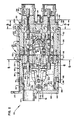
- Referring now to the drawings wherein like reference numerals designate identical or corresponding parts throughout the several views, and more particularly to FIGURE l, a jack device in accordance with the present invention is designated generally as 20.
Device 20 is attached topanel 22 with a screw 23 (see FIGURE ll) passing throughopening 24 and threading into a hole inpanel 22.Jack device 20 includes ahousing 26, aconducting mechanism 28, andmechanism 30 for supportingconducting mechanism 28 with respect to housing 26 (see FIGURE 2). In addition,jack device 20 may include amechanism 32 for monitoring the signal passing throughdevice 20.Monitoring mechanism 32 includes asignal conducting cable 34 extending to, for example, a connectingjack 36 shown mounted topanel 22. -
Housing 26 includes front andrear modules Modules more sleeves 50 extend outwardly from thesecond end 46 offront module 38. Afront module 38 having a single sleeve is shown in FIGURE 7, while afront module 38 having twosleeves 50 is shown in FIGURE 8.Sleeves 50 are formed to receive a con necting plug from a coaxial cable as shown, for example, in FIGURE l at 52. Connectingsleeves 54 are attached tosecond end 48 ofrear module 40.Jack device 20 is intended to have twosleeves 54 attached torear module 40, but as shown in FIGURES 9 and l0, the sleeves may assume various forms. For example, FIGURE 9 shows a conventional bayonetconnector receiving sleeve 56 and acrimp sleeve 58 wherein the center conductor of a coaxial cable is attached to conductor l57 fastened inrear module 40.Sleeve 58 is crimped so as to make contact with and hold the shield of the cable. In FIGUREl0 connecting sleeve 54 is shown in the form of a threadedsleeve 60 for receiving a standard threaded connector, and is also shown in the form of alarger crimp sleeve 58′. It is understood that numerous combinations of one or twosleeves 50 of various sizes may be formed as a part offront module 38 and that various combinations of the numerous connectingsleeves 54 may be attached torear module 40 to give the assembly substantial versatility with respect to various termination mechanisms for coaxial cables or other appropriate signal carrying mechanisms. Front andrear modules shells 62 which are attached together with a pair of nut andbolt assemblies 64 as shown in FIGURE l. Front andrear modules sleeves 50 and connectingsleeves 54 are preferably conductive. - As shown in FIGURES l and 2,
front module 38 is formed as two parallel cylinders 66 held together in the parallel configuration by forward and rearwardtransverse bulkheads cylindrical passageway 72 therethrough which is axially aligned with anysleeve 50 extending fromfront bulkhead 68 on the side opposite cylinder 66. The rearward portion ofpassageway 72 is inclined in a frusto-conical shape to expand toward the rear. Just rearward ofrear bulkhead 70 each cylinder wall includes a pair ofopenings 74. Also, the inclined wall ofpassageway 72 includes a plurality of regularly spaced grooves 76 (see FIGURE 5). There is at least onegroove 76 running axially and aligned with eachopening 74.Grooves 76 are needed to receiveprotuberances 272 onsupport members 252 during assembly. Thesupport members 252 fit intopassageways 72 until the inclined side wall ofsupport member 252 mates with the inclined wall ofpassageway 72 and theprotuberances 272 fit intoopenings 74 to snugly hold thesupport member 252 in the end ofpassageway 72. In theregion 78 between forward andrearward bulkheads empty region 78 is then available for switch mechanism l56 as discussed hereinafter. Each cylinder 66 also includes ashort recess portion 80 at the rearward end in order to fit into a mating recess ll4 in theforward bulkhead 98 ofrear module 40. Anotherrecess portion 82 is formed in the outer sidewall of cylinders 66 just rearward offorward bulkhead 68.Recess portion 82 extends along almost half the distance between forward andrearward bulkheads rectangular openings 84 are formed in therecess portions 82 of each cylinder 66 and are centered on the horizontal cross sectional plane of thejack device 20.Recess portion 82 is formed to receiveground spring 86.Ground spring 86 has end portions 88 (see FIGURE l) which wrap around the cylinders 66. Each end portion 88 includes adetent 90 which protrudes through anopening 84. When aplug 52 is inserted intosleeve 50, the outer surface ofplug 52 contacts detent 90 and forces endportion 86 outwardly so that a spring force is maintained at the contact betweenground spring 86 and theplug 52. Thecenter portion 92 ofground spring 86 extends between the end portions 88 and is fastened in place with one of nut and boltcombinations 64. Centered at the forward end ofground spring 86 is a tab 94 (see FIGURE 6) which is bent inwardly for the purpose of contacting a resistor l74 as discussed hereinafter. -
Rear module 40 also includes a pair ofparallel cylinders 96 held in the parallel configuration by aforward bulkhead 98 and a rearward connecting segment l00. Connecting segment l00 includes a pair of spaced apart ridges l02 and l04 running transversely aboutrear module 40. Ridges l02 and l04 have the general shape offorward bulkhead 98 and function in combination with it to longitudinally retainrear module 40 toshells 62.Cylinders 96 have cylindrical passageways l06 extending therethrough and being axially aligned withpassageways 72 offorward module 38. The rearward ends of passageways l06 are larger than the rest of passageways l06 and have an inclined frusto-conical wall l08 expanding toward the rearward end. As withfront module 38, wall l08 has a plurality of regularly spaced axially running grooves ll0 (see FIGURE 3). A pair of openings ll2 pass through the walls of eachcylinder 96 and are aligned with a pair of grooves ll0.Support member 250 includes aprotuberance 264 which slides along grooves ll0 during installation. The outer side surface ofsupport member 250 is frusto-conically shaped and mates with wall l08 at the point when theprotuberances 264 enter into openings ll2 to retainsupport member 250 in place. -
Forward bulkhead 98 ofrear module 40 has a recess ll4 in end 44 to receive end 42 offorward module 38. The outer perimeter ofbulkhead 98 fits aboutrecess 80 ofmodule 38 while the end 42 ofmodule 38 fits into recess ll4 ofrear module 40. Therear end 48 ofrear module 40 has sleeve-like flanges ll6 extending as projections ofcylinders 96. Flanges ll6 have thinner walls than the ends ofcylinders 96 at the end of passageways l08 so that there is a circular shoulder ll8 against which the end flanges l20 of connectingsleeves 54 butt. Flanges ll6 are bent over flanges l20 to retain connectingsleeves 54 torear module 40. As shown in FIGURES l and l2, about the upper, inner one-third of the cylindrical wall ofcylinders 96 is missing to present an open area betweenforward bulkhead 98 and the forward wall l22 of connecting portion l00. The remainder of the facing walls ofcylinders 96 have flat vertical surfaces l24 as shown in FIGURE l2. The end of surfaces l24 includes an inward projection l26 for the purpose of retaining insulating holder l28 for monitoring components as described hereinafter. - Forward and
rear modules shells 62. Eachshell 62 is identical. As shown in FIGURE 2,shell 62 includes grooves l30, l32 and l34.Rear bulkhead 70 offorward module 38 fits in groove l30.Forward bulkhead 68 butts against the forward end l36 ofshell 62. In this way,front module 38 is prevented from moving longitudinally with respect toshells 62. -
Front bulkhead 98 ofrear module 40 fits in groove l32. Ridges l02 and l04 fit in wider groove l34.Bulkhead 98 and ridges l02 and l04 in grooves l32 and l34 retainrear module 40 against longitudinal movement with respect to shell 62.Shell 62 also includes front and rear posts l38 and l40, respectively. Front post l38 includes a forward extending portion l42 for fitting between cylinders 66 ofmodule 38. Front post l38 also includes a rear groove l44 for receiving insulating holdingmembers 200 of switch mechanism l56 as discussed hereinafter. Rear post l40 includes a forward tongue l46 for fitting into the rear end of holdingmembers 200. Forward and rear posts l38 and l40 extend inwardly sufficiently far so that they butt against one another when upper andlower shells 62 are fastened together. - An electrical schematic of
jack device 20 is shown in FIGURE l3. A signal is input at connecting end l48 of conductor l49 which is also connected to inductor l5l. If a plug has been inserted in connecting end l52, then a signal passes directly throughjack device 20 along conductor l50. If no plug has been inserted in either connecting end l52 or l54, then switch mechanism l56 directs the signal to conductor l58 for output through inductor l59 and conductor l57 at connecting end l60. Ifjack device 20 is used as a pass through connector, then a signal cannot only be input at connecting end l48 and passed through to connecting end l52, but also another signal may be input at connecting end l60 and passed through to connecting end l54. In that case, switch mechanism l56 would be disconnected from both conducting paths. - If a plug is not present in connecting ends l52 and l54, then end portion l62 of spring conductor l64 is forced against conductor l50 and directs the signal through conductor l64 to opposite end portion l66 which is likewise forced against conductor l58. If a plug is inserted in connecting end l52 as discussed hereinafter lever conductor l68 moves end portion l62 of spring conductor l64 away from conductor l50. Lever conductor l68 similarly moves end portion l66 from conductor l58 if a plug is inserted in connecting end l54. In the case when lever conductor l68 moves end portion l62 away from conductor l50, the circuit which includes connecting end l60, inductor l59, conductor l58, end portion l66 and switching conductor l64 is completed to ground l72 at end portion l70 and lever conductor l68 through resistor l74. Similarly, lever conductor l68 includes end portion l76 which functions to move switching end portion l66 if a plug is inserted in connecting end l54 and is connected to ground l72 through resistor l74.
- Any signal conducted along line l50 may be monitored through resistor l80 via line l82. Resistor l82 is connected to inductor l84 via line l86. Inductor l84 is grounded at line l88. A monitoring line l87 is center tapped to inductor l84 and leads to connecting end l89.
- It is understood that the monitor branch of the circuit shown in FIGURE l3 is optional, as is connecting end l54. Furthermore, there are cases when a simple pass through circuit is all that is appropriate.
- Several of the conductors, the switch assembly and the monitoring assembly are shown in FIGURE 2. The conductors are discussed further hereinafter with reference to support members. The switch assembly l56 is shown in greater detail in FIGURE ll. The switch assembly l56 includes spring conductor l64 and lever conductor l68 as held by a holding assembly l90. Spring conductor l64 is an elongated flat sheet having end portions l92 and a central portion l94 with cantilever portions l96 extending therebetween. Central portion l94 is held in a pair of aligned, facing arcuate slots l98 in holding members 200 (see FIGURE 6). Central portion l94 curves rearwardly so that cantilever portion l96 extends diagonally rearwardly and sidewardly. At the end of cantilever portion l96, it mates with end portion l92 to extend sidewardly and slightly forwardly to forwardly extending
arcuate end 202. The conductors l50 and l58 are cylindrical at thelocations 202 and 204, where the arcuate ends l62 and l66 make contact with them. The curvatures of the arcuate ends l62 and l66 are approximately perpendicular to the curvatures of thecylindrical portions 202 and 204. - Lever conductor l68 also has
end portions 206 and acentral portion 208 connected together by cantilever portions 2l0. A dielectric sleeve 2l2 is formed about a segment of each of the cantilever portions 2l0 to provide a surface against which plug 52 may slide without making electrical contact with lever conductor l68. Similar to spring conductor l64, thecentral portion 208 of lever conductor l68 is curved rearwardly and held by holdingmembers 200 in facing slots 2l4. Cantilever portions 2l0 extend rearwardly and slightly sidewardly from central portion 204. Theend portions 206 are formed arcuately with inward curvatures. It is noted thatcentral portion 208 has upper and lower tabs 2l6. There are upper and lower tabs for symmetry. One of the tabs contacts one end of resistor l74. Tabs 2l6 are located along the centerline ofjack device 20 and are bent rearwardly at the top and bottom of central portion 204. One of tabs 2l6 contacts one end of resistor l74 whiletab 94 ofground spring 92 contacts the other end of resistor l74. - Holding
members 200 are identical. Each has protrusions 2l8 slightly sidewardly from the centerline ofjack device 20 andopenings 220 for receiving the protrusions 2l8 of the other holdingmember 200. The openings are slightly off the centerline in the other direction from protrusions 2l8. As indicated, holdingmembers 200 have facing slots l98 for receiving spring conductor l64 and facing slots 2l4 for receiving lever conductor l68. Slots 2l4 are forwardly of slots l98 and anopening 222 located between the pairs of slots extends completely through the holding members for the purpose of receiving the bolt of bolt andnut combination 64 in order to hold holdingmembers 200 toshells 62. The forward end of holdingmembers 200 includes atongue 224 for fitting in groove l44 of post l38 onshell 62. In a similar fashion, the rearward end of holdingmembers 200 includes agroove 226 for receiving tongue l46 of post l40 ofshell 62. Holdingmembers 200 also includearms 228 which extend in both sidewardly directions at the rear end of holdingmembers 200. Aretainer flange 230 extends in the direction of the arm on the other holdingmember 200. Theretainer flanges 228 prevent theend portions 206 of lever conductor l68 from contacting the end portions l92 of spring conductor l64. - When
plug 52 is inserted insleeve 50, the outer surface ofplug 52 contacts dielectric sleeve 2l2 and forces the cantilever portion 2l0 of lever conductor l68 inwardly. Whenend portion 206 of lever conductor l68 contacts cantilever portion l96 of spring conductor l64, it forces cantilever portion l96 inwardly thereby breaking contact between arcuate end l62 of end portion l92 andcylindrical portion 202 of conductor l50. It is noted thatend portion 206 is arcuate and rubs along the inclined cantilever portion l96 thereby wiping and cleaning the contacting surface between the two conductors. Similarly, since end portion l92 angles forwardly and applies a spring force oncylindrical portion 202, when the spring force is overcome by lever conductor l68, arcuate end l62 wipes along and cleans the contacting surface between end l62 andcylindrical portion 202. - The monitoring branch of the circuit shown in FIGURE l3, as indicated previously, is an optional feature. With reference to FIGURES 2 and l2, inductor l84 is shown. In addition, the conductors l82 and l86 leading to resistor l80 are indicated. Support member l28 holds inductor l84 and resistor l80. Support member l28 has a substantially
rectangular base 232 to fit in the space between the straight walls l24 ofcylinders 96 and betweenforward bulkhead 98 and wall l22 ofrear module 40. Apost 234 rises abovebase 232 and includes anopening 236 for receiving the bolt of a nut andbolt combination 64. The bottom ofbase 232 and the top ofpost 234 contact oppositeshells 62.Base 232 includes a plurality of either recesses or channels 238 for receivingprongs 240 of anend member 242 connected to the ground wire ofcable 34. Oneprong 244 of the plurality ofprongs 240 extends throughbase 232 to provide a terminal for connection with wire l88 from inductor l84. - Since
jack device 20 is intended to be an interconnecting mechanism for passing a signal from one transmission line to another, a crucial consideration is power transmission through the connecting device. In a direct current circuit, power is reduced at each resistive component. In an alternating current circuit, such as any circuit in which thepresent jack device 20 would be used, the same is true except for the resistive component one must more generally consider the effects of inductance and capacitance and consequently, the important parameter is impedance. Just as with any direct current circuit, in going from one conductor to another it is important to keep contact resistance low so that the resistance per unit length of the conductors is not increased at the contact, so with an alternating current circuit it is important to match the impedance from one device to another. Since impedance is related inversely to frequency, the problem of matching impedance is evermore difficult as frequencies rise. Consider the voltage diagrams in FIGURES l4A and l4B. In a simple circuit having, for example, simply resistance per unit length, current and voltage would be in phase and on a phase diagram voltage could be represented as shown in FIGURE A. The power through such a simple circuit would be P = VI. In an alternating current circuit having an inductor and a capacitor as well as resistance per unit length, the phase relationship of voltage and current is altered by the inductor and capacitor. A phase diagram of typical component voltages is illustrated in FIGURE l4B. A resolution of the voltage as shown in FIGURE l4B is shown in FIGURE l4C. In this case, voltage will lead current by a phase angle φ. With respect to power transmission, there would be loss due to the reactive components, namely, the inductor and the capacitor which have caused the phase difference between the voltage and current. In other words, V = VR/cos φ or voltage would have to be increased by a factor of l/cos φ to obtain the same output power as that of the simple circuit described with respect to FIGURE l4A. The mismatch of reactive components has thus caused a power loss in transmission. - The present invention has addressed not only the performance parameter of impedance matching, but has also matched capacitive and inductive reactances so as to keep the voltage and current in phase through the jack device and thereby reduce any reactive power loss. The present invention represents a recognition not only of the necessity to match impedances from one conductive component to another throughout the transmission circuit in the jack device, but also of the desirability to equalize inductive and capacitive components of the impedance. For example, the end portion l92 of spring conductor l64 in switch mechanism l56 and the
cylindrical wall 202 of conductor l50 provides surfaces of a type commonly found in capacitors. Consequently, there is an induced capacitive effect injack device 20 as a result of the relationship of the switch surfaces. To counteract the capacitive reactance introduced by those surfaces, an inductor l5l is introduced between conductors l49 and l50. Similarly, inductor l59 is installed between conductors l57 and l58 to provide inductive reactance to counter the capacitive reactance of the other side of spring conductor l64. - To determine the success of the indicated concept, an RG 59 B/
U 75 ohm coaxial cable was connected to incoming connecting end l48 and aprecision 75 ohm termination device was connected to connecting end l60. A time domain reflectometer was then appropriately connected to the coaxial cable. As a signal was transmitted, the graph of FIGURE l5 showing the impedance characteristics of the circuit was developed. Rises above the straight 75 ohm line are due to inductive reactance, while rises below the line are due to capacitive reactance. It is noted that the present invention resulted in both capacitive and inductive reactances which approximately canceled so as to relatively closely maintain an average 75 ohm impedance throughjack device 20. - As a confirming test, a return loss measurement at frequencies from l00 hertz to 600 megahertz was made. The present invention held impedance within five percent of the impedance of the connected coaxial cable up to a frequency of 452 megahertz. Thus, not only has impedance been matched with the present jack device, but it has been done so throughout a wide range of frequencies.
- When analyzing the distributed effects of geometry to the contributions to impedance, another part of
jack device 20 which must be carefully considered are the support structures between the signal carrying conductors and the ground mechanism, preferably the conductive housing ofpresent jack device 20. In a cable, the impedance between a conductor and a coaxial shield depends on the distance between the two items. If a substance other than air is inserted somewhere between the two items, for example, to hold the central conductor with respect to the outer shield, then a dielectric constant somewhat less efficient than air has been introduced and a different impedance results. Prior art connectors show solid disk-like support members between a central conductor and an outer conductive housing. The present invention is recognition of the possibility of not only varying the distance between the central conductor and the wall of the housing, or varying the substance for the support member thereby varying the dielectric constant, but is also recognition of the advantage which is achievable by using support members of geometries which incorporate both a dielectric material and air cavities between the central conductor and the wall of the conductive housing. - Conductor l49 is supported by
support member 246 with respect to connectingsleeve 54 and is further supported bysupport member 250 with respect torear module 40. Conductor l50 is supported bysupport member 252 with respect tofront module 38. Conductors l57 and l58 in the other cylinders of front andrear modules knurled portion 254 as well as enlarged ends at the rear end ofsupport member 246 and the front end ofsupport member 250 in order to rigidly retain conductor l49 to supportmembers sleeve 54 and cylindrical wall l06. Similarly, conductor l50 has a forward end shaped to receive a straight conductor and has aknurled portion 256 for making good mechanical contact withsupport member 252 and keeping conductor l50 centered with respect tocylindrical wall 72 and cylindrical wall l06 of front andrear modules - As shown in FIGURES 3 and 4,
support members support member 250.Support member 250 has a central core 258 with an axial opening for receiving and holding conductor l49. A plurality ofspokes 260 extend radially outwardly from core 258. The ends of each spoke 260 fit into one of thegrooves 262 in the wall ofcylinder 96. An opposing pair ofspokes 260 each have aprotuberance 264 for fitting into the openings ll2 in the wall ofcylinder 96. It is noted that the air spaces betweenspokes 260 preferably have a wedge-type shape are located in a space defined by the opposite ends ofsupport member 250 and the wall ofcylinder 96, and are regularly spaced about core 258. -
Support member 252 has a somewhat different shape as shown in FIGURE 5.Support member 252 has acentral core 266 and anouter ring 268 concentric with thecentral core 266 with the plurality ofspokes 270 extending betweencore 266 andring 268. Again, a pair ofprotuberances 272 are formed opposite from one another on the outer side ofring 270 and are aligned withgrooves 76 inwall 72 and project intoopenings 74. Theair cavities 274 are regularly spaced aboutcentral core 266 and form a portion of a wedge-like shape. - It is noted that the present invention makes it possible to use a desired material having a given dielectric constant while yet achieving impedance matching simply by designing a shape to include sufficient regularly spaced air cavities in order to alter the effective insulating quality of the support member.
-
Jack device 20 is ordinarily attached to apanel 22 with one or more screws 23. Depending on the types of connectingsheeves 54 used at the rear end ofrearward module 40, appropriate plugs, connectors or termination devices are installed thereto. Assuming then that a coaxial connection is made to both connectingsleeves 54 onrear module 40, a signal in at conductor l49 passes through inductor l5l and conductor l50 to spring conductor l64 of switch mechanism l56. From spring conductor l64, the signal continues along conductor l58 and through inductor l59 to conductor l57 and then to the connected cable. - If a
plug 52 is inserted insleeve 50 offorward module 38, plug 52 contacts dielectric sleeve 2l2 and forces endportion 206 of lever conductor l68 against cantilever portion l96 of spring conductor l64. Before arcuate end l62 of end portion l92 of spring conductor l64 breaks contact withcylindrical portion 202 of conductor l50,end portion 206 makes contact with cantilever portion l96. In this way, the circuit including conductor l57, inductor l59, conductor l58 terminates to ground through resistor l74 via spring con ductor l64 and lever conductor l68. The housing ofjack device 20 is conductive and is electrical ground. Withplug 52 installed, a signal passes from conductor l49 through inductor l5l to conductor l50 and plug 52. The outer shell ofplug 52 is grounded by springingdetent 90 ofground spring 82 outwardly. - In a
jack device 20 having asecond sleeve 50 infront module 38, a plug inserted therein would function similar to insertion ofplug 52 as just described. In that case, however, signals from the cables connected to the connectingsleeves 54 would pass directly through to cables connected to the connectingsleeves 50. -
Jack device 20 may also include a monitoring circuit for recreating an input signal or for other purposes. If a plug is inserted injack 36, any signal being conducted along conductor l49 passes through inductor l5l to resistor l80, inductor l84 and out on conductor l87 ofcable 34 to jack 36. Signal amplitude is appropriately small so as not to affect power transmission. - As discussed hereinbefore,
jack device 20 takes uniquely into account impedance matching characteristics of the support members for the conductors and also matches impedance in a way which results in approximately equivalent inductive and capacitive reactances. The present jack device not only provides for superior electrical performance, but also provides superior versatility with respect to a variety of configurations and, consequently, applications. The housing is modular. Theforward module 38 may include one ormore sleeves 50 of various diameters.Rear module 40 may include various connectingsleeves 54. Uses range from direct pass through to patching in another line and terminating the output line through a resistor to ground, as well as to monitoring. Other uses and applications have also been indicated. In spite of the details of structure and function which have been set forth at length, it is nevertheless also understood that changes may be made. Consequently, equivalent modifications are also within the principle of the present invention to the full extent extended by the general meaning of the terms in which the appended claims are expressed.
Claims (19)
a housing having signal-in means for connecting with said first coaxial cable and first and second signal-out means for connecting with at least one of said termination means of said second coaxial cable and said plug of said third coaxial cable, respectively, said housing including grounding means for connecting to said first, second and third coaxial cables;
means for conducting an electrical signal from said signal-in means to said first and second signal-out means, said conducting means including means for switching said signal from said first signal-out means to said second signal-out means on insertion of said plug, said conducting means further including a second characteristic impedance having approximately equal inductive and capacitive reactive components; and
means for supporting said conducting means with respect to said housing.
a housing having signal-in means for connecting with said termination means of said first coaxial cable and signal-out means for connecting with said termination means of said second coaxial cable, said housing including a passageway having a wall, said passageway for extending between said signal-in means and said signal-out means, said housing including grounding means for connecting to said first and second coaxial cables;
means for conducting an electrical signal from said signal-in means to said signal-out means, said conducting means including an elongated conductor member; and
means for supporting said conducting means with respect to said housing, said supporting means including a dielectric support member for supporting said conductor member, said support member having opposite ends and an outer edge for fitting against said wall, said wall and said opposite ends of said support member defining a space, said space including said support member and a plurality of regularly spaced cavities with respect to said conductor member, said support member having a second characteristic impedance, said second characteristic impedance being approximately equal to said first characteristic impedance.
a housing having signal-in means for connecting with said first coaxial cable and first and second signal-out means for connecting with at least one of said termination means of said second coaxial cable and said plug of said third coaxial cable, respectively, said housing including grounding means for connecting to said first, second and third coaxial cables;
means for conducting an electrical signal from said signal-in means to said first and second signal-out means, said conducting means including means for switching said signal from said first signal-out means to said second signal-out means on insertion of said plug, said conducting means further including a second characteristic impedance having approximately equal inductive and capacitive reactive components; and
means for supporting said conducting means with respect to said housing, said supporting means having a third characteristic impedance, said second and third characteristic impedances being approximately equal to said first characteristic impedance.
a housing having signal-in means for connecting with said first termination means of said first coaxial cable and first and second signal-out means for connecting with said second termination means of said second coaxial cable and said plug of said third coaxial cable, respectively, said housing also including a plurality of passageways having walls, said passageways for extending between said signal-in means and said first and second signal-out means, said housing being conductive for maintaining a ground continuity with said first, second and third shields;
means for conducting an electrical signal along one of first and second conductive paths, said first path extending between said signal-in means and said first signal-out means, said first path for being in electrical com munication with said first and second central conductors, said second path extending between said signal-in means and said second signal-out means, said second path for being in electrical communication with said first and third central conductors, said conducting means including switching means for closing electrical continuity to ground before opening electrical continuity in said first path on insertion of said plug; and
means for supporting said conducting means with respect to said housing.
a housing
signal-in means for connecting said first coaxial cable to said housing;
first signal-out means for connecting said second coaxial cable to said housing;
second signal-out means including means sized to accommodate insertion of said plug into said housing at a first insertion location and connecting said third coaxial cable to said housing;
grounding means for electrically grounding said first, second and third cables when said cables are connected to said housing;
conducting means for conducting an electrical signal from said signal-in means to said first and second signal-out means, said conducting means including switch means for switching said signal from said first signal-out means for said second signal-out means upon insertion of said plug at said first location, said conducting means having components with an inductive reactance selected to balance a capacitive reactance of said switch means.
Applications Claiming Priority (2)
| Application Number | Priority Date | Filing Date | Title |
|---|---|---|---|
| US808501 | 1985-12-13 | ||
| US06/808,501 US4749968A (en) | 1985-12-13 | 1985-12-13 | Jack device |
Publications (3)
| Publication Number | Publication Date |
|---|---|
| EP0230746A2 true EP0230746A2 (en) | 1987-08-05 |
| EP0230746A3 EP0230746A3 (en) | 1988-09-28 |
| EP0230746B1 EP0230746B1 (en) | 1995-02-22 |
Family
ID=25198956
Family Applications (1)
| Application Number | Title | Priority Date | Filing Date |
|---|---|---|---|
| EP86309708A Expired - Lifetime EP0230746B1 (en) | 1985-12-13 | 1986-12-12 | Jack device |
Country Status (11)
| Country | Link |
|---|---|
| US (1) | US4749968A (en) |
| EP (1) | EP0230746B1 (en) |
| JP (1) | JP2593860B2 (en) |
| KR (1) | KR940002900B1 (en) |
| AT (1) | ATE118927T1 (en) |
| AU (1) | AU593473B2 (en) |
| CA (1) | CA1267198C (en) |
| DE (1) | DE3650244T2 (en) |
| ES (1) | ES2070814T3 (en) |
| HK (1) | HK1007637A1 (en) |
| IL (1) | IL80953A (en) |
Cited By (7)
| Publication number | Priority date | Publication date | Assignee | Title |
|---|---|---|---|---|
| EP0380210A2 (en) * | 1989-01-27 | 1990-08-01 | Adc Telecommunications, Inc. | Delay compensated jack |
| GB2238672A (en) * | 1989-11-17 | 1991-06-05 | Amp Inc | Shunting device for use in electrical connectors |
| EP0480788A3 (en) * | 1990-10-12 | 1993-05-19 | Augat Inc. | Self-operative electrical shunting contact and method for forming same |
| GB2267000A (en) * | 1992-05-07 | 1993-11-17 | Jonathan Barrie Williams | Audio insert point doubler. |
| WO1995012228A1 (en) * | 1993-10-29 | 1995-05-04 | Adc Telecommunications, Inc. | Jack module |
| US6139369A (en) * | 1997-07-31 | 2000-10-31 | Telefonaktiebolaget Lm Ericsson | Coaxial connector for equipment in a transmission network |
| EP2843776B1 (en) * | 2013-08-28 | 2018-09-26 | Spinner GmbH | U-link connector for RF signals with integrated bias circuit |
Families Citing this family (59)
| Publication number | Priority date | Publication date | Assignee | Title |
|---|---|---|---|---|
| US5214673A (en) * | 1989-08-04 | 1993-05-25 | Adc Telecommunications, Inc. | Digital cross connect assembly |
| AU630934B2 (en) * | 1989-08-04 | 1992-11-12 | Adc Telecommunications, Incorporated | Digital cross-connect assembly |
| US5147992A (en) * | 1990-06-12 | 1992-09-15 | Adc Telecommunications, Inc. | Jack assembly |
| CA2040398A1 (en) * | 1990-06-12 | 1991-12-13 | Byron Eriksen | Jack assembly |
| US5170327A (en) * | 1990-11-05 | 1992-12-08 | Adc Telecommunications, Inc. | Distal distribution frame module |
| US5233501A (en) * | 1992-02-27 | 1993-08-03 | Telect, Inc. | Digital telecommunication network cross-connect module having a printed circuit board connected to jack switches |
| BR9207121A (en) * | 1992-04-02 | 1995-12-12 | Adc Telecommunications Inc | Miniature coaxial plug module |
| WO1994008429A1 (en) * | 1992-10-05 | 1994-04-14 | Adc Telecommunications, Inc. | Jack module assembly |
| US5482469A (en) * | 1993-07-21 | 1996-01-09 | Trimm, Inc. | Dual monitor self-contained six port digital signal cross-connect module |
| US5577924A (en) * | 1995-01-09 | 1996-11-26 | Adc Telecommunications, Inc. | Jack module with inductive monitor |
| US5546282A (en) * | 1995-05-02 | 1996-08-13 | Telect, Inc. | Telecommunication network digital cross-connect panels having insertable modules with printed circuit board mounted coaxial jack switches |
| US5594347A (en) * | 1995-05-22 | 1997-01-14 | Adc Telecommunications, Inc. | Non-invasive testing of video signals with a jack module and amplification circuit |
| AU5737796A (en) * | 1995-05-22 | 1996-12-11 | Adc Telecommunications, Incorporated | Switching coax jack with amplified monitor |
| JPH09115620A (en) * | 1995-10-17 | 1997-05-02 | Fujitsu Ltd | Coaxial conversion connector |
| US5676570A (en) * | 1996-03-15 | 1997-10-14 | Minnesota Mining And Manufacturing Company | "F" port interface connector |
| US5913701A (en) * | 1997-02-28 | 1999-06-22 | Adc Telecommunications, Inc. | DSX module with removable switching jack |
| US5964607A (en) * | 1997-04-04 | 1999-10-12 | Adc Telecommunications, Inc. | Coaxial switching jack with sliding center conductor |
| US5885096A (en) * | 1997-04-04 | 1999-03-23 | Adc Telecommunications, Inc. | Switching coaxial jack |
| US5882217A (en) * | 1997-10-10 | 1999-03-16 | Lucent Technologies Inc. | Coaxial jack with an internal switch mechanism |
| US6081109A (en) * | 1997-11-07 | 2000-06-27 | Xantech Corporation | Current sensing device |
| US6045378A (en) * | 1998-03-27 | 2000-04-04 | Adc Telecommunications, Inc. | Switching coaxial jack with impedance matching |
| US6146167A (en) * | 1998-09-16 | 2000-11-14 | Telect, Inc. | Telecommunication module having edge mounted jack and switch therefor |
| US6587354B1 (en) * | 1998-09-18 | 2003-07-01 | Duane B. Kutsch | Telecommunication assembly |
| US6116961A (en) | 1998-11-12 | 2000-09-12 | Adc Telecommunications, Inc. | Jack assembly |
| MXPA01010093A (en) * | 1999-04-06 | 2002-05-06 | Adc Telecommunications Inc | Dsx module with removable jack. |
| US6589062B1 (en) | 1999-04-06 | 2003-07-08 | Adc Telecommunications, Inc. | DSX module with removable jack |
| US6545562B2 (en) * | 2001-02-09 | 2003-04-08 | Adc Telecommunications, Inc. | Plug connector for cable television network and method of use |
| US6632106B2 (en) | 2001-07-24 | 2003-10-14 | Adc Telecommunications, Inc. | Jack; jack assembly; and methods |
| US6554652B1 (en) | 2002-02-15 | 2003-04-29 | Adc Telecommunications, Inc. | Jack assembly including baluns interface; and methods |
| US20030168235A1 (en) * | 2002-03-07 | 2003-09-11 | Todd Loeffelholz | EMI shielded module |
| US6830486B2 (en) * | 2002-07-19 | 2004-12-14 | Adc Telecommunications, Inc. | Digital switching cross-connect module |
| US6830487B2 (en) * | 2002-07-19 | 2004-12-14 | Adc Telecommunications, Inc. | Pin jack for a digital switching cross-connect module |
| US7070457B2 (en) | 2002-07-19 | 2006-07-04 | Adc Telecommunications, Inc. | Telecommunications connector |
| US7239699B2 (en) * | 2002-07-19 | 2007-07-03 | Adc Telecommunications, Inc. | Monitor network for a digital switching cross-connect module |
| US6743044B2 (en) * | 2002-08-14 | 2004-06-01 | Adc Telecommunications, Inc. | Cross-connect jumper assembly having tracer lamp |
| US7095844B2 (en) * | 2002-10-18 | 2006-08-22 | Adc Telecommunications, Inc. | High density DSX system |
| US6893299B2 (en) * | 2002-10-18 | 2005-05-17 | Adc Telecommunications, Inc. | Termination panel with fanning strips |
| US6918793B2 (en) * | 2002-10-18 | 2005-07-19 | Adc Telecommunications, Inc. | Rear access DSX system |
| US20050026506A1 (en) * | 2002-11-18 | 2005-02-03 | Trompeter Electronics, Inc. | Modular cross-connect with hot-swappable modules |
| US6752665B2 (en) * | 2002-11-18 | 2004-06-22 | Trompeter Electronics, Inc. | Modular cross-connect with removable switch assembly |
| US20040105219A1 (en) * | 2002-12-03 | 2004-06-03 | Mcclellan Terry E. | Chassis for housing telecommunications components |
| US6679728B1 (en) * | 2002-12-27 | 2004-01-20 | Insert Enterprise Co., Ltd. | Mini BNC connector |
| US6848948B1 (en) * | 2003-11-03 | 2005-02-01 | Adc Telecommunications, Inc. | Jack with modular mounting sleeve |
| US7182502B2 (en) * | 2004-06-21 | 2007-02-27 | Adc Telecommunications, Inc. | Press-in place LED for a digital switching cross-connect module |
| US7029323B1 (en) * | 2004-09-27 | 2006-04-18 | Adc Telecommunications, Inc. | High density mount for a co-axial connector |
| US20060067068A1 (en) * | 2004-09-27 | 2006-03-30 | Petersen Cyle D | Digital cross-connect system and rack arrangement |
| US7175455B2 (en) * | 2005-04-15 | 2007-02-13 | Adc Telecommunications, Inc. | High density coaxial switching jack |
| US7074080B1 (en) * | 2005-04-21 | 2006-07-11 | Adc Telecommunications, Inc. | Modular mounting sleeve for jack |
| WO2006115813A1 (en) * | 2005-04-21 | 2006-11-02 | Adc Telecommunications, Inc. | Modular mounting sleeve for jack |
| US7238035B2 (en) * | 2005-06-14 | 2007-07-03 | Trompeter Electronics, Inc. | Normal-through jack with monitor and test ports |
| US7244131B1 (en) | 2006-04-21 | 2007-07-17 | Adc Telecommunications, Inc. | High density coaxial jack |
| US7591677B2 (en) * | 2006-04-21 | 2009-09-22 | Adc Telecommunications, Inc. | High density coaxial jack and panel |
| US7393249B2 (en) * | 2006-04-21 | 2008-07-01 | Trompeter Electronics, Inc. | Interconnection and monitoring module |
| US7540787B2 (en) * | 2007-04-12 | 2009-06-02 | Adc Telecommunications, Inc. | Flex-X module with board mounted baluns |
| KR100963424B1 (en) * | 2008-07-23 | 2010-06-15 | 한국전자통신연구원 | Scalable video decoder and controlling method for the same |
| US8760875B2 (en) * | 2009-11-24 | 2014-06-24 | Telect, Inc. | High density digital signal cross-connect system |
| CN102097698A (en) * | 2009-12-09 | 2011-06-15 | 苏州华旃航天电器有限公司 | Medium supporting structure applied to radio-frequency coaxial connector |
| US9285557B2 (en) | 2012-06-27 | 2016-03-15 | Tyco Electronics Raychem Bvba | High density telecommunications chassis with cable management |
| US9521766B2 (en) | 2012-06-27 | 2016-12-13 | CommScope Connectivity Belgium BVBA | High density telecommunications systems with cable management and heat dissipation features |
Citations (5)
| Publication number | Priority date | Publication date | Assignee | Title |
|---|---|---|---|---|
| US2478781A (en) * | 1944-06-02 | 1949-08-09 | Bell Telephone Labor Inc | Circuit maker and breaker |
| US2779005A (en) * | 1955-09-06 | 1957-01-22 | Northern Electric Co | Coaxial jack |
| US2958054A (en) * | 1958-11-24 | 1960-10-25 | Amphenol Borg Electronics Corp | Impedance terminated coaxial line switch apparatus |
| US3182270A (en) * | 1962-11-02 | 1965-05-04 | Amphenol Borg Electronics Corp | Multiple position coaxial switch with angularly spaced radial channels |
| US3360747A (en) * | 1965-07-19 | 1967-12-26 | Cooke Engineering Company | Self-normaling jack barrel assembly with impedance balancing element |
Family Cites Families (14)
| Publication number | Priority date | Publication date | Assignee | Title |
|---|---|---|---|---|
| CA658424A (en) * | 1963-02-26 | Don-Lan Electronics | High frequency switching unit | |
| US3109997A (en) * | 1961-07-10 | 1963-11-05 | Bell Telephone Labor Inc | Double circuit coaxial jack with automatic cross-connection upon plug removal and automatic termination of idle line upon plug insertion |
| US3372349A (en) * | 1965-08-13 | 1968-03-05 | Amphenol Corp | Modular coaxial switch |
| US3373360A (en) * | 1966-01-27 | 1968-03-12 | Curtis L. Wilson | Automatic coaxial switch |
| US3529264A (en) * | 1967-12-07 | 1970-09-15 | Cook Eng Co | Shielded electrical switching jack with impedance balancing network |
| US3946390A (en) * | 1975-04-07 | 1976-03-23 | Motorola, Inc. | Radio frequency connector system for portable radios |
| US4087151A (en) * | 1976-07-28 | 1978-05-02 | Magnetic Controls Company | Printed circuit card edge connector with normalling contacts |
| US4099825A (en) * | 1977-08-24 | 1978-07-11 | Kings Electronics Co., Inc. | Coaxial adapter |
| US4224485A (en) * | 1978-10-16 | 1980-09-23 | Bell Telephone Laboratories, Incorporated | Telephone jack |
| US4286335A (en) * | 1979-11-08 | 1981-08-25 | Motorola, Inc. | Coaxial dual antenna connection arrangement for communications apparatus |
| JPS613106Y2 (en) * | 1980-04-10 | 1986-01-31 | ||
| US4477134A (en) * | 1981-08-14 | 1984-10-16 | Hewlett-Packard Company | Electrostatic discharge protected integrated circuit module |
| US4575694A (en) * | 1984-03-05 | 1986-03-11 | Allied Corporation | Coaxial connector |
| US4559421A (en) * | 1984-03-05 | 1985-12-17 | Allied Corporation | Electrical connector including a make-before-break switch arrangement |
-
1985
- 1985-12-13 US US06/808,501 patent/US4749968A/en not_active Expired - Lifetime
-
1986
- 1986-12-11 CA CA525047A patent/CA1267198C/en not_active Expired
- 1986-12-12 AT AT86309708T patent/ATE118927T1/en not_active IP Right Cessation
- 1986-12-12 ES ES86309708T patent/ES2070814T3/en not_active Expired - Lifetime
- 1986-12-12 DE DE3650244T patent/DE3650244T2/en not_active Expired - Lifetime
- 1986-12-12 EP EP86309708A patent/EP0230746B1/en not_active Expired - Lifetime
- 1986-12-13 KR KR1019860010737A patent/KR940002900B1/en not_active IP Right Cessation
- 1986-12-13 JP JP61299107A patent/JP2593860B2/en not_active Expired - Lifetime
- 1986-12-15 IL IL80953A patent/IL80953A/en not_active IP Right Cessation
- 1986-12-15 AU AU66534/86A patent/AU593473B2/en not_active Expired
-
1998
- 1998-06-25 HK HK98106754A patent/HK1007637A1/en not_active IP Right Cessation
Patent Citations (5)
| Publication number | Priority date | Publication date | Assignee | Title |
|---|---|---|---|---|
| US2478781A (en) * | 1944-06-02 | 1949-08-09 | Bell Telephone Labor Inc | Circuit maker and breaker |
| US2779005A (en) * | 1955-09-06 | 1957-01-22 | Northern Electric Co | Coaxial jack |
| US2958054A (en) * | 1958-11-24 | 1960-10-25 | Amphenol Borg Electronics Corp | Impedance terminated coaxial line switch apparatus |
| US3182270A (en) * | 1962-11-02 | 1965-05-04 | Amphenol Borg Electronics Corp | Multiple position coaxial switch with angularly spaced radial channels |
| US3360747A (en) * | 1965-07-19 | 1967-12-26 | Cooke Engineering Company | Self-normaling jack barrel assembly with impedance balancing element |
Cited By (10)
| Publication number | Priority date | Publication date | Assignee | Title |
|---|---|---|---|---|
| EP0380210A2 (en) * | 1989-01-27 | 1990-08-01 | Adc Telecommunications, Inc. | Delay compensated jack |
| EP0380210A3 (en) * | 1989-01-27 | 1990-12-19 | Adc Telecommunications, Inc. | Delay compensated jack |
| GB2238672A (en) * | 1989-11-17 | 1991-06-05 | Amp Inc | Shunting device for use in electrical connectors |
| GB2238672B (en) * | 1989-11-17 | 1994-04-20 | Amp Inc | Shunting device for use in electrical connectors |
| EP0480788A3 (en) * | 1990-10-12 | 1993-05-19 | Augat Inc. | Self-operative electrical shunting contact and method for forming same |
| GB2267000A (en) * | 1992-05-07 | 1993-11-17 | Jonathan Barrie Williams | Audio insert point doubler. |
| WO1995012228A1 (en) * | 1993-10-29 | 1995-05-04 | Adc Telecommunications, Inc. | Jack module |
| AU678048B2 (en) * | 1993-10-29 | 1997-05-15 | Adc Telecommunications, Incorporated | Jack module |
| US6139369A (en) * | 1997-07-31 | 2000-10-31 | Telefonaktiebolaget Lm Ericsson | Coaxial connector for equipment in a transmission network |
| EP2843776B1 (en) * | 2013-08-28 | 2018-09-26 | Spinner GmbH | U-link connector for RF signals with integrated bias circuit |
Also Published As
| Publication number | Publication date |
|---|---|
| DE3650244T2 (en) | 1995-08-10 |
| KR940002900B1 (en) | 1994-04-06 |
| AU6653486A (en) | 1987-06-18 |
| CA1267198A (en) | 1990-03-27 |
| AU593473B2 (en) | 1990-02-08 |
| CA1267198C (en) | 1990-03-27 |
| JP2593860B2 (en) | 1997-03-26 |
| DE3650244D1 (en) | 1995-03-30 |
| EP0230746B1 (en) | 1995-02-22 |
| HK1007637A1 (en) | 1999-04-16 |
| ATE118927T1 (en) | 1995-03-15 |
| JPS62195868A (en) | 1987-08-28 |
| IL80953A (en) | 1990-04-29 |
| ES2070814T3 (en) | 1995-06-16 |
| EP0230746A3 (en) | 1988-09-28 |
| KR870006684A (en) | 1987-07-14 |
| US4749968A (en) | 1988-06-07 |
Similar Documents
| Publication | Publication Date | Title |
|---|---|---|
| EP0230746A2 (en) | Jack device | |
| KR100250677B1 (en) | Miniature coax jack module | |
| CA2262727C (en) | Low crosstalk connector configuration | |
| US5246378A (en) | Coaxial jack assembly | |
| US6250960B1 (en) | Female to female CATV splice connector | |
| US6602097B1 (en) | High frequency electrical connector | |
| US6814624B2 (en) | Telecommunications jack assembly | |
| US5348491A (en) | Jack module | |
| EP1096619B1 (en) | Modular telecommunication jack-type connector with crosstalk reduction | |
| CA1290038C (en) | Patch connector | |
| JPH025377A (en) | Digital communication network cross connection module | |
| CA2144704A1 (en) | Combination connector | |
| JPH07201379A (en) | Patch connector | |
| US5340333A (en) | Shielded modular adapter | |
| US5137469A (en) | Hybrid connector for standard coaxial cable and other wiring systems | |
| US5904579A (en) | Right-angle adaptor for coaxial jacks | |
| AU778544B2 (en) | Modular jack having a plug-positioning member | |
| US5496196A (en) | CDDI connector for high-speed networks of voice and data transmissions | |
| CA2322929A1 (en) | Electrical connector with internal shield and filter | |
| JPH1083857A (en) | Connector unit for transmission network | |
| US7116779B1 (en) | Network interface device for high speed data lines | |
| EP3916929B1 (en) | A data transmission connector and a corresponding connector assembly, electric cable and use thereof | |
| JPH02504684A (en) | Tap type electrical connector assembly | |
| WO1996035243A1 (en) | Fault voltage isolator | |
| AU752830B2 (en) | Low-crosstalk electrical connector grouping like conductors together |
Legal Events
| Date | Code | Title | Description |
|---|---|---|---|
| PUAI | Public reference made under article 153(3) epc to a published international application that has entered the european phase |
Free format text: ORIGINAL CODE: 0009012 |
|
| AK | Designated contracting states |
Kind code of ref document: A2 Designated state(s): AT BE CH DE ES FR GB GR IT LI LU NL SE |
|
| PUAL | Search report despatched |
Free format text: ORIGINAL CODE: 0009013 |
|
| AK | Designated contracting states |
Kind code of ref document: A3 Designated state(s): AT BE CH DE ES FR GB GR IT LI LU NL SE |
|
| 17P | Request for examination filed |
Effective date: 19890308 |
|
| 17Q | First examination report despatched |
Effective date: 19910502 |
|
| GRAA | (expected) grant |
Free format text: ORIGINAL CODE: 0009210 |
|
| AK | Designated contracting states |
Kind code of ref document: B1 Designated state(s): AT BE CH DE ES FR GB GR IT LI LU NL SE |
|
| REF | Corresponds to: |
Ref document number: 118927 Country of ref document: AT Date of ref document: 19950315 Kind code of ref document: T |
|
| ITF | It: translation for a ep patent filed |
Owner name: BARZANO'E ZANARDO S.P.A. |
|
| REF | Corresponds to: |
Ref document number: 3650244 Country of ref document: DE Date of ref document: 19950330 |
|
| ET | Fr: translation filed | ||
| REG | Reference to a national code |
Ref country code: ES Ref legal event code: FG2A Ref document number: 2070814 Country of ref document: ES Kind code of ref document: T3 |
|
| REG | Reference to a national code |
Ref country code: GR Ref legal event code: FG4A Free format text: 3016098 |
|
| PLBE | No opposition filed within time limit |
Free format text: ORIGINAL CODE: 0009261 |
|
| STAA | Information on the status of an ep patent application or granted ep patent |
Free format text: STATUS: NO OPPOSITION FILED WITHIN TIME LIMIT |
|
| 26N | No opposition filed | ||
| REG | Reference to a national code |
Ref country code: GB Ref legal event code: IF02 |
|
| PGFP | Annual fee paid to national office [announced via postgrant information from national office to epo] |
Ref country code: LU Payment date: 20021024 Year of fee payment: 17 |
|
| PGFP | Annual fee paid to national office [announced via postgrant information from national office to epo] |
Ref country code: NL Payment date: 20021112 Year of fee payment: 17 |
|
| PGFP | Annual fee paid to national office [announced via postgrant information from national office to epo] |
Ref country code: BE Payment date: 20030116 Year of fee payment: 17 |
|
| PG25 | Lapsed in a contracting state [announced via postgrant information from national office to epo] |
Ref country code: LU Free format text: LAPSE BECAUSE OF NON-PAYMENT OF DUE FEES Effective date: 20031212 |
|
| PG25 | Lapsed in a contracting state [announced via postgrant information from national office to epo] |
Ref country code: BE Free format text: LAPSE BECAUSE OF NON-PAYMENT OF DUE FEES Effective date: 20031231 |
|
| BERE | Be: lapsed |
Owner name: *ADC TELECOMMUNICATIONS INC. Effective date: 20031231 |
|
| PG25 | Lapsed in a contracting state [announced via postgrant information from national office to epo] |
Ref country code: NL Free format text: LAPSE BECAUSE OF NON-PAYMENT OF DUE FEES Effective date: 20040701 |
|
| NLV4 | Nl: lapsed or anulled due to non-payment of the annual fee |
Effective date: 20040701 |
|
| PGFP | Annual fee paid to national office [announced via postgrant information from national office to epo] |
Ref country code: GR Payment date: 20051024 Year of fee payment: 20 |
|
| PGFP | Annual fee paid to national office [announced via postgrant information from national office to epo] |
Ref country code: AT Payment date: 20051104 Year of fee payment: 20 Ref country code: GB Payment date: 20051104 Year of fee payment: 20 |
|
| PGFP | Annual fee paid to national office [announced via postgrant information from national office to epo] |
Ref country code: FR Payment date: 20051201 Year of fee payment: 20 |
|
| PGFP | Annual fee paid to national office [announced via postgrant information from national office to epo] |
Ref country code: SE Payment date: 20051202 Year of fee payment: 20 |
|
| PGFP | Annual fee paid to national office [announced via postgrant information from national office to epo] |
Ref country code: ES Payment date: 20051213 Year of fee payment: 20 |
|
| PGFP | Annual fee paid to national office [announced via postgrant information from national office to epo] |
Ref country code: CH Payment date: 20051216 Year of fee payment: 20 |
|
| PGFP | Annual fee paid to national office [announced via postgrant information from national office to epo] |
Ref country code: IT Payment date: 20051222 Year of fee payment: 20 |
|
| PGFP | Annual fee paid to national office [announced via postgrant information from national office to epo] |
Ref country code: DE Payment date: 20051230 Year of fee payment: 20 |
|
| PG25 | Lapsed in a contracting state [announced via postgrant information from national office to epo] |
Ref country code: GB Free format text: LAPSE BECAUSE OF EXPIRATION OF PROTECTION Effective date: 20061211 |
|
| PG25 | Lapsed in a contracting state [announced via postgrant information from national office to epo] |
Ref country code: ES Free format text: LAPSE BECAUSE OF EXPIRATION OF PROTECTION Effective date: 20061213 |
|
| REG | Reference to a national code |
Ref country code: GB Ref legal event code: PE20 |
|
| REG | Reference to a national code |
Ref country code: CH Ref legal event code: PL |
|
| EUG | Se: european patent has lapsed | ||
| REG | Reference to a national code |
Ref country code: ES Ref legal event code: FD2A Effective date: 20061213 |