EP0238024A2 - Depositing tungsten on a semiconductor substrate - Google Patents
Depositing tungsten on a semiconductor substrate Download PDFInfo
- Publication number
- EP0238024A2 EP0238024A2 EP87103807A EP87103807A EP0238024A2 EP 0238024 A2 EP0238024 A2 EP 0238024A2 EP 87103807 A EP87103807 A EP 87103807A EP 87103807 A EP87103807 A EP 87103807A EP 0238024 A2 EP0238024 A2 EP 0238024A2
- Authority
- EP
- European Patent Office
- Prior art keywords
- tungsten
- deposited
- substrate
- masking film
- film
- Prior art date
- Legal status (The legal status is an assumption and is not a legal conclusion. Google has not performed a legal analysis and makes no representation as to the accuracy of the status listed.)
- Granted
Links
Images
Classifications
-
- H—ELECTRICITY
- H01—ELECTRIC ELEMENTS
- H01L—SEMICONDUCTOR DEVICES NOT COVERED BY CLASS H10
- H01L21/00—Processes or apparatus adapted for the manufacture or treatment of semiconductor or solid state devices or of parts thereof
- H01L21/02—Manufacture or treatment of semiconductor devices or of parts thereof
- H01L21/04—Manufacture or treatment of semiconductor devices or of parts thereof the devices having at least one potential-jump barrier or surface barrier, e.g. PN junction, depletion layer or carrier concentration layer
- H01L21/18—Manufacture or treatment of semiconductor devices or of parts thereof the devices having at least one potential-jump barrier or surface barrier, e.g. PN junction, depletion layer or carrier concentration layer the devices having semiconductor bodies comprising elements of Group IV of the Periodic System or AIIIBV compounds with or without impurities, e.g. doping materials
- H01L21/20—Deposition of semiconductor materials on a substrate, e.g. epitaxial growth solid phase epitaxy
- H01L21/205—Deposition of semiconductor materials on a substrate, e.g. epitaxial growth solid phase epitaxy using reduction or decomposition of a gaseous compound yielding a solid condensate, i.e. chemical deposition
-
- H—ELECTRICITY
- H01—ELECTRIC ELEMENTS
- H01L—SEMICONDUCTOR DEVICES NOT COVERED BY CLASS H10
- H01L21/00—Processes or apparatus adapted for the manufacture or treatment of semiconductor or solid state devices or of parts thereof
- H01L21/02—Manufacture or treatment of semiconductor devices or of parts thereof
- H01L21/04—Manufacture or treatment of semiconductor devices or of parts thereof the devices having at least one potential-jump barrier or surface barrier, e.g. PN junction, depletion layer or carrier concentration layer
- H01L21/18—Manufacture or treatment of semiconductor devices or of parts thereof the devices having at least one potential-jump barrier or surface barrier, e.g. PN junction, depletion layer or carrier concentration layer the devices having semiconductor bodies comprising elements of Group IV of the Periodic System or AIIIBV compounds with or without impurities, e.g. doping materials
- H01L21/28—Manufacture of electrodes on semiconductor bodies using processes or apparatus not provided for in groups H01L21/20 - H01L21/268
- H01L21/283—Deposition of conductive or insulating materials for electrodes conducting electric current
- H01L21/285—Deposition of conductive or insulating materials for electrodes conducting electric current from a gas or vapour, e.g. condensation
- H01L21/28506—Deposition of conductive or insulating materials for electrodes conducting electric current from a gas or vapour, e.g. condensation of conductive layers
- H01L21/28512—Deposition of conductive or insulating materials for electrodes conducting electric current from a gas or vapour, e.g. condensation of conductive layers on semiconductor bodies comprising elements of Group IV of the Periodic System
- H01L21/28556—Deposition of conductive or insulating materials for electrodes conducting electric current from a gas or vapour, e.g. condensation of conductive layers on semiconductor bodies comprising elements of Group IV of the Periodic System by chemical means, e.g. CVD, LPCVD, PECVD, laser CVD
- H01L21/28562—Selective deposition
-
- H—ELECTRICITY
- H01—ELECTRIC ELEMENTS
- H01L—SEMICONDUCTOR DEVICES NOT COVERED BY CLASS H10
- H01L21/00—Processes or apparatus adapted for the manufacture or treatment of semiconductor or solid state devices or of parts thereof
- H01L21/02—Manufacture or treatment of semiconductor devices or of parts thereof
- H01L21/04—Manufacture or treatment of semiconductor devices or of parts thereof the devices having at least one potential-jump barrier or surface barrier, e.g. PN junction, depletion layer or carrier concentration layer
- H01L21/18—Manufacture or treatment of semiconductor devices or of parts thereof the devices having at least one potential-jump barrier or surface barrier, e.g. PN junction, depletion layer or carrier concentration layer the devices having semiconductor bodies comprising elements of Group IV of the Periodic System or AIIIBV compounds with or without impurities, e.g. doping materials
- H01L21/30—Treatment of semiconductor bodies using processes or apparatus not provided for in groups H01L21/20 - H01L21/26
- H01L21/31—Treatment of semiconductor bodies using processes or apparatus not provided for in groups H01L21/20 - H01L21/26 to form insulating layers thereon, e.g. for masking or by using photolithographic techniques; After treatment of these layers; Selection of materials for these layers
- H01L21/3205—Deposition of non-insulating-, e.g. conductive- or resistive-, layers on insulating layers; After-treatment of these layers
- H01L21/32051—Deposition of metallic or metal-silicide layers
-
- H—ELECTRICITY
- H01—ELECTRIC ELEMENTS
- H01L—SEMICONDUCTOR DEVICES NOT COVERED BY CLASS H10
- H01L21/00—Processes or apparatus adapted for the manufacture or treatment of semiconductor or solid state devices or of parts thereof
- H01L21/70—Manufacture or treatment of devices consisting of a plurality of solid state components formed in or on a common substrate or of parts thereof; Manufacture of integrated circuit devices or of parts thereof
- H01L21/71—Manufacture of specific parts of devices defined in group H01L21/70
- H01L21/768—Applying interconnections to be used for carrying current between separate components within a device comprising conductors and dielectrics
- H01L21/76838—Applying interconnections to be used for carrying current between separate components within a device comprising conductors and dielectrics characterised by the formation and the after-treatment of the conductors
- H01L21/76877—Filling of holes, grooves or trenches, e.g. vias, with conductive material
- H01L21/76879—Filling of holes, grooves or trenches, e.g. vias, with conductive material by selective deposition of conductive material in the vias, e.g. selective C.V.D. on semiconductor material, plating
Abstract
Description
- The present invention relates to the deposition of tungsten upon a semiconductor substrate.
- In semiconductor LSIs (Large Scale Integrated Circuits), polycrystalline silicon has been widely employed for fabricating electrodes and/or electrical wiring. However, there is a limit to the degree to which the electrical resistance of polycrystalline silicon can be reduced, because it is a semiconductor. Therefore, a refractory metal, such as tungsten, or its silicide, has been employed in place of the polycrystalline silicon.
- Fabrication of a tungsten electrode or tungsten wiring will be explained below with reference to Fig. 1, which is a schematic cross-sectional view.
- The whole surface of a
silicon semiconductor substrate 1 is coated with a masking film of a phospho-silicate glass (referred to hereinafter as PSG) or silicon dioxide (referred to hereinafter as SiO₂) generally as much as approximately 1µm thick. Themasking film 2 is patterned using a lithography technique so that an opening, such as acontact hole 3, is provided at a portion of the substrate on which tungsten is to be deposited, to expose a portion 1ʹ of the substrate. Next, thesubstrate 1, having themasking film 2 thereon, is loaded into a CVD (Chemical Vapour Deposition) apparatus. A reaction gas, i.e. a mixture of tungsten hexafluoride (referred to hereinafter as WF₆) gas and a hydrogen (referred to hereinafter as H₂) gas, is fed into the apparatus, and gas pressure is reduced to 0.1 to 0.5 Torr, and then thesubstrate 1 having themasking film 2 thereon is heated. - Chemical reactions given by the following formulae take place.
2 WF₆ + 3 Si = 2 W + 3 SiF₄ (1)
WF₆ + 3 H₂ = W + 6 HF (2) - The exposed silicon of the
substrate 1 is active to reduce the WF₆ and produces SiF₄ and W (tungsten). The produced tungsten is deposited upon the surface of the exposed portion 1ʹ of thesilicon substrate 1. This reducing reaction (1) does not take place on the SiO₂ of themasking film 2, therefore little tungsten is deposited on themasking film 2. Thus, selective deposition of the tungsten is performed. However, when the deposited tungsten forms a film on the exposed portion 1ʹ of thesilicon substrate 1, the tungsten film so formed prevents the silicon substrate from further reacting with the WF₆ gas. Thus, tungsten deposition cannot proceed beyond a thickness of deposited tungsten of approximately 1000 Angstroms. Therefore, in order to maintain deposition of tungsten, H₂ gas is added in the WF₆ gas. The chemical reaction involved is given by formula (2). WF₆ is reduced to provide HF (hydrofluoric acid) and W (tungsten). The reaction (2) not only produces tungsten additionally on the previously deposited tungsten but also newly forms tungsten nucleii on the surface of themasking film 2, and the nucleii keep on growing to form a tungsten film. If the tungsten nucleii form a film, the tungsten film imperils the function of the masking film, i.e. electrical isolation, and the film is not easily removed. Therefore, the reaction (2) must be discontinued before tungsten film is formed on themasking film 2. This means thattungsten film 4 formed on the exposed silicon substrate 1ʹ cannot be deposited to a thickness greater than 3000 Angstroms (typically 2000 Angstroms). This thickness is sufficient for the depositedtungsten 4 to be an electrical conductor. However, the big difference between the heights of the surfaces of the masking film 2 (approximately 1µm) and the deposited tungsten 4 (approximately 2000 Angstroms) causes problems in later processing for fabricating a reliablycontinuous aluminium wiring 5 on those surfaces for connecting the deposited tungsten, i.e. an electrode, to an external connection. In other words, the accuracy of the photolithography of thealuminium film 5 deposited on the non-flat surface is, of course, deteriorated, and also the sharp edge of themasking film 2 may cause discontinuity of the aluminium deposition. This problem becomes impermissibly serious for fabricating VLSIs (Very Large Scale Integrated Circuits) of sub-micron order. Therefore, there is a need for a method of providing a thick tungsten film whose surface can form a substantially flat surface together with the surface of the masking film. - An embodiment of the present invention can provide a method of selectively depositing thick tungsten on a silicon semiconductor substrate, such that the surface of the deposited tungsten and the surface of a masking film can be level with each other, in order to allow an accurate and reliable patterning of aluminium film thereon.
- In an embodiment of the present invention tungsten is selectively deposited by the use of a CVD method on an exposed portion of a semiconductor substrate through an opening in a masking film of phospho-silicate glass (PSG) or silicon dioxide (SiO₂) coated on the silicon substrate. At the same time, some tungsten is deposited also on the masking film, though the rate of deposition is slow. Before a tungsten film is formed on the masking film, the tungsten deposited on the masking film is removed. The removal of tungsten from the masking film may be carried out by heating the substrate in a hydrogen gas, which produces hydrofluoric acid (HF) from residual WF₆ therein, or by wet etching in a HF solution, or by a dry etching in a nitrogen trifluoride (NF₃) gas. Next, a further deposition of tungsten, upon the previously deposited tungsten on the substrate, is provided by repeating the previous deposition process. By repetition of the above-described processes, i.e. deposition and removal, a tungsten deposition (on the substrate) can reach a thickness of 1µm, which is substantially the same as that of the masking film. Thus, the surfaces of the deposited tungsten and the masking film form a practically flat common surface. Therefore, in a later process, an aluminium film can be deposited and patterned on this flat surface accurately and reliably, and thus fabrication of VLSIs of sub-micron order can be achieved.
- Reference is made, by way of example, to the accompanying drawings, in which:-
- Fig. 1 is a schematic cross-sectional view for assistance in explaining the deposition of tungsten on a semiconductor substrate by a previous method; and
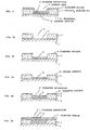
- Figs. 2a to 2e are schematic cross-sectional views illustrating steps in the deposition of tungsten according to embodiments of the present invention.
- Fig. 2a shows a
semiconductor substrate 1, which would in general be of silicon containing some dopants, as is widely known, and amasking film 2, which would be coated on the whole surface of thesubstrate 1. Themasking film 2 is generally made of PSG or SiO₂, and approximately 1µm thick. An opening, i.e. acontact hole 3, is made by patterning themasking film 2 using a lithography technique. So, a portion 1ʹ of thesubstrate 1 at the bottom of thecontact hole 3 is exposed. Thesubstrate 1 coated with themasking film 2 is loaded into a CVD apparatus and CVD-processed according to the following conditions:
WF₆ supplied at a flow rate of : 100 cc/min. H₂ supplied at a flow rate of : 6 litre/min. Gas pressure : 0.3 to 0.5 Torr
Temperature of the substrate : 325°C. - Chemical reactions taking place therein are the same as those indicated by formulae (1) and (2) above.
- The SiO₂ of the masking film is etched out by the produced HF, so the surface of the film is caused to be rough. Microscopically sharp edges of the rough surface are apt to have tungsten nucleii grow thereon. Processing is continued until an island structure, which consists of many nucleii 6 of tungsten, is produced and seen on the surface of the
masking film 2, as illustrated in Fig. 2b. The CVD processing is then stopped. At this time, 2000 to 3000 Angstroms thickness oftungsten 4 has been deposited on the exposed surface 1ʹ of thesilicon substrate 1. It takes approximately 30 minutes for these reactions. If CVD deposition were to continue after the island structure is produced, the undesired tungsten nucleii 6 on themasking film 2 would grow quickly, and the selectivity of deposition would be reduced. - Next, the tungsten nucleii 6 on the
masking film 2 are removed, as illustrated in Fig. 2c. The removal may be carried out by one of the following methods. - The first method involves the use of hydrogen gas. When the above-described tungsten deposition process is stopped a hydrogen gas is fed into the CVD apparatus with the loaded
substrate 1 kept as it was. The conditions are as follows:
H₂ gas supply : 400 cc/min.
Temperature of the substrate : 325°C
Gas pressure : 0.3 to 0.5 Torr. - The H₂ gas reacts with a fluorine atom produced from the WF₆ in the previous deposition process and still remaining in the CVD apparatus, to produce HF gas in the apparatus. This HF gas etches the SiO₂ content in the surface of the
masking film 2 which is supporting the tungsten nucleii 6 thereon; thus the tungsten nucleii 6 are removed. It takes typically 10 minutes for this processing. This method is an efficient method because the same apparatus can be continuously used for the deposition and removal of the tungsten without a break and with no need to open the apparatus and take out the substrate. - The second method of removing the tungsten nucleii 6 involves wet etching with HF solution. The etchant(s) used and the processing involved can be chosen from the following:
- a. Washing in a dilute HF solution and then in water;
- b. Washing in a H₂O₂ (hydrogen peroxide) solution, then in a dilute HF solution, then in water;
- c. Washing in a solution of NH₄OH (ammonia) + H₂O₂, then in a dilute HF solution, and then in water.
- Both the H₂O₂ and NH₄OH + H₂O₂ are active to etch the tungsten nucleii. The HF acts in the same way as described above.
- The third method of removing the tungsten nucleii 6 involves dry etching in a NF₃ + H₂ gas in the CVD apparatus following the tungsten deposition process. The conditions are as follows:
NF₃ gas supply : 100 cc/min.
H₂ gas supply : 400 cc/min.
. Gas pressure : 0.1 to 0.2 Torr
Temperature of the substrate : 400 to 500°C. - HF gas is then produced as shown below
2 NF₃ + 3 H₂ = N₂ + 6 HF. - The produced HF gas acts in the same way as described above. In the process for tungsten nucleii removal, the masking film may be etched by a few hundred Angstroms.
- After removing the undesirably deposited tungsten nucleii 6 on the
masking film 2, the same deposition processing as that carried out previously is carried out again. Thus a tungsten film 4ʹ is additionally deposited on the previously depositedfilm 4. Upon the etched surface 2ʹ of themasking film 2, new tungsten nucleii 6ʹ are undesirably deposited again in the same way as in the first deposition process. This state is illustrated in Fig.2d. Then, the tungsten nucleii 6ʹ on themasking film 2 are again removed, by removal processing as described above. After repeating the processes of tungsten deposition and removal several times, for example three times, the height oftungsten deposition 4+4ʹ+4ʺ... in thecontact hole 3 becomes substantially the same as the height of themasking film 2, and thus a flat surface, as shown in Fig. 2e, is provided. A deposition thickness of as much as 1µm can be achieved after proper repetition of the processings. - An aluminium film 5ʹ (Fig. 2e) is deposited on the practically flat surface of the deposited
tungsten 4+4ʹ+4ʺ... and themasking film 2, and then patterned, for example by a sputtering and a lithography technique, for connecting the deposited tungsten to other parts of a semiconductor device or to an external connection. Owing to the good flatness of the surface on which the aluminium wiring is patterned, the wiring is fabricated accurately and reliably. Thus, embodiments of the present invention can contribute to the achievement of VLSIs of sub-micron order. - Although, in the description of embodiments of the present invention given above, reference is made to a contact hole, in which tungsten is deposited as an electrode, it will be apparent that embodiments of the invention can be applied to the deposition of tungsten for wirings as well.
- An embodiment of the present invention provides a method of selectively depositing tungsten upon a silicon semiconductor substrate, on which a masking film of PSG or SiO₂ is coated and patterned to provide an opening for forming an electrode or wiring therein. On a portion of the substrate in the opening, approximately 2000 Angstroms thickness of tungsten is deposited by a CVD method, in which tungsten hexafluoride gas and hydrogen gas are used and the substrate is heated. As a result of this processing, some tungsten nucleii are deposited on the surface of the masking film as well. Before the nucleii form a film, the deposition processing is discontinued and a hydrogen gas is fed in to produce hydrofluoric acid, which etches the surface of the masking film, thus to remove the tungsten nucleii thereon. The above-described processings, i.e. deposition and removal of tungsten, are repeated several times until the heights of the deposited tungsten and the masking film become practically equal, forming a flat surface. Aluminium film is deposited on the flat surface and patterned by lithography. Thus, the flat aluminium deposition allows the fabrication of accurate and reliable wiring, which is important for achievement of VLSIs of sub-micron order.
Claims (6)
forming a patterned mask on the substrate;
depositing tungsten upon a part of the substrate not covered by the patterned mask;
removing tungsten deposited upon the surface of the patterned mask; and
depositing further tungsten, after the removing step, upon the tungsten deposited upon the substrate.
Applications Claiming Priority (2)
| Application Number | Priority Date | Filing Date | Title |
|---|---|---|---|
| JP58753/86 | 1986-03-17 | ||
| JP61058753A JPS62216224A (en) | 1986-03-17 | 1986-03-17 | Selectively growing method for tungsten |
Publications (3)
| Publication Number | Publication Date |
|---|---|
| EP0238024A2 true EP0238024A2 (en) | 1987-09-23 |
| EP0238024A3 EP0238024A3 (en) | 1990-03-14 |
| EP0238024B1 EP0238024B1 (en) | 1993-11-24 |
Family
ID=13093297
Family Applications (1)
| Application Number | Title | Priority Date | Filing Date |
|---|---|---|---|
| EP87103807A Expired - Lifetime EP0238024B1 (en) | 1986-03-17 | 1987-03-16 | Depositing tungsten on a semiconductor substrate |
Country Status (4)
| Country | Link |
|---|---|
| US (1) | US4804560A (en) |
| EP (1) | EP0238024B1 (en) |
| JP (1) | JPS62216224A (en) |
| KR (1) | KR900003612B1 (en) |
Cited By (6)
| Publication number | Priority date | Publication date | Assignee | Title |
|---|---|---|---|---|
| EP0326217A1 (en) * | 1988-01-29 | 1989-08-02 | Koninklijke Philips Electronics N.V. | Method of manufacturing a semiconductor device |
| EP0345400A1 (en) * | 1988-06-08 | 1989-12-13 | L'air Liquide, Societe Anonyme Pour L'etude Et L'exploitation Des Procedes Georges Claude | Selective CVD for maufacturing semiconductor devices |
| DE3933194A1 (en) * | 1988-10-11 | 1990-04-12 | Mitsubishi Electric Corp | Formation of tungsten contacts to silicon diffused regions - reduces series resistance of contacts and results in planar surface for interconnection pattern |
| EP0371854A2 (en) * | 1988-11-30 | 1990-06-06 | Mcnc | Method for selectively depositing refractory metal on semiconductor substrates |
| WO1991003834A1 (en) * | 1989-09-05 | 1991-03-21 | Mcnc | Method for selectively depositing material on substrates |
| US5112439A (en) * | 1988-11-30 | 1992-05-12 | Mcnc | Method for selectively depositing material on substrates |
Families Citing this family (79)
| Publication number | Priority date | Publication date | Assignee | Title |
|---|---|---|---|---|
| US4963511A (en) * | 1987-11-30 | 1990-10-16 | Texas Instruments Incorporated | Method of reducing tungsten selectivity to a contact sidewall |
| US4997520A (en) * | 1988-06-10 | 1991-03-05 | Texas Instruments Incorporated | Method for etching tungsten |
| JPH0810682B2 (en) * | 1988-10-25 | 1996-01-31 | 三菱電機株式会社 | Method for manufacturing semiconductor device |
| US5231055A (en) * | 1989-01-13 | 1993-07-27 | Texas Instruments Incorporated | Method of forming composite interconnect system |
| US5357991A (en) * | 1989-03-27 | 1994-10-25 | Semitool, Inc. | Gas phase semiconductor processor with liquid phase mixing |
| US5238500A (en) * | 1990-05-15 | 1993-08-24 | Semitool, Inc. | Aqueous hydrofluoric and hydrochloric acid vapor processing of semiconductor wafers |
| JP2721023B2 (en) * | 1989-09-26 | 1998-03-04 | キヤノン株式会社 | Deposition film formation method |
| EP0420597B1 (en) * | 1989-09-26 | 1996-04-24 | Canon Kabushiki Kaisha | Process for forming a deposited film by use of alkyl aluminum hydride and process for preparing semiconductor device |
| US5015323A (en) * | 1989-10-10 | 1991-05-14 | The United States Of America As Represented By The Secretary Of Commerce | Multi-tipped field-emission tool for nanostructure fabrication |
| US6375741B2 (en) * | 1991-03-06 | 2002-04-23 | Timothy J. Reardon | Semiconductor processing spray coating apparatus |
| KR930002673B1 (en) * | 1990-07-05 | 1993-04-07 | 삼성전자 주식회사 | Growing method of metal having high melting point |
| US5077236A (en) * | 1990-07-02 | 1991-12-31 | Samsung Electronics Co., Ltd. | Method of making a pattern of tungsten interconnection |
| US5843233A (en) * | 1990-07-16 | 1998-12-01 | Novellus Systems, Inc. | Exclusion guard and gas-based substrate protection for chemical vapor deposition apparatus |
| US5620525A (en) * | 1990-07-16 | 1997-04-15 | Novellus Systems, Inc. | Apparatus for supporting a substrate and introducing gas flow doximate to an edge of the substrate |
| DE69034137D1 (en) * | 1990-10-01 | 2004-06-03 | St Microelectronics Srl | Manufacture of contact connections for all-over CVD deposition and etching back |
| US5064686A (en) * | 1990-10-29 | 1991-11-12 | Olin Corporation | Sub-valent molybdenum, tungsten, and chromium amides as sources for thermal chemical vapor deposition of metal-containing films |
| KR950012918B1 (en) * | 1991-10-21 | 1995-10-23 | 현대전자산업주식회사 | Contact filling method using secondary deposition of selective tungsten thin film |
| US5200360A (en) * | 1991-11-12 | 1993-04-06 | Hewlett-Packard Company | Method for reducing selectivity loss in selective tungsten deposition |
| US5328868A (en) * | 1992-01-14 | 1994-07-12 | International Business Machines Corporation | Method of forming metal connections |
| US5306666A (en) * | 1992-07-24 | 1994-04-26 | Nippon Steel Corporation | Process for forming a thin metal film by chemical vapor deposition |
| GB9219267D0 (en) * | 1992-09-11 | 1992-10-28 | Inmos Ltd | Manufacture of semiconductor devices |
| GB9219281D0 (en) * | 1992-09-11 | 1992-10-28 | Inmos Ltd | Manufacture of semiconductor devices |
| US5663098A (en) * | 1992-10-08 | 1997-09-02 | Sandia Corporation | Method for deposition of a conductor in integrated circuits |
| US5776827A (en) * | 1993-08-27 | 1998-07-07 | Yamaha Corporation | Wiring-forming method |
| JPH07115130A (en) * | 1993-10-14 | 1995-05-02 | Toshiba Corp | Manufacture of semiconductor device |
| US5430328A (en) * | 1994-05-31 | 1995-07-04 | United Microelectronics Corporation | Process for self-align contact |
| US5489552A (en) * | 1994-12-30 | 1996-02-06 | At&T Corp. | Multiple layer tungsten deposition process |
| US5599739A (en) * | 1994-12-30 | 1997-02-04 | Lucent Technologies Inc. | Barrier layer treatments for tungsten plug |
| US5954911A (en) * | 1995-10-12 | 1999-09-21 | Semitool, Inc. | Semiconductor processing using vapor mixtures |
| US5681423A (en) | 1996-06-06 | 1997-10-28 | Micron Technology, Inc. | Semiconductor wafer for improved chemical-mechanical polishing over large area features |
| US6245668B1 (en) * | 1998-09-18 | 2001-06-12 | International Business Machines Corporation | Sputtered tungsten diffusion barrier for improved interconnect robustness |
| JP3403357B2 (en) | 1999-06-03 | 2003-05-06 | 株式会社半導体先端テクノロジーズ | Wiring forming method and wiring forming apparatus |
| US6534866B1 (en) | 2000-04-13 | 2003-03-18 | Micron Technology, Inc. | Dual damascene interconnect |
| US7005372B2 (en) * | 2003-01-21 | 2006-02-28 | Novellus Systems, Inc. | Deposition of tungsten nitride |
| US7141494B2 (en) * | 2001-05-22 | 2006-11-28 | Novellus Systems, Inc. | Method for reducing tungsten film roughness and improving step coverage |
| US7955972B2 (en) | 2001-05-22 | 2011-06-07 | Novellus Systems, Inc. | Methods for growing low-resistivity tungsten for high aspect ratio and small features |
| US7589017B2 (en) * | 2001-05-22 | 2009-09-15 | Novellus Systems, Inc. | Methods for growing low-resistivity tungsten film |
| US9076843B2 (en) | 2001-05-22 | 2015-07-07 | Novellus Systems, Inc. | Method for producing ultra-thin tungsten layers with improved step coverage |
| US6635965B1 (en) * | 2001-05-22 | 2003-10-21 | Novellus Systems, Inc. | Method for producing ultra-thin tungsten layers with improved step coverage |
| US7262125B2 (en) * | 2001-05-22 | 2007-08-28 | Novellus Systems, Inc. | Method of forming low-resistivity tungsten interconnects |
| US6844258B1 (en) | 2003-05-09 | 2005-01-18 | Novellus Systems, Inc. | Selective refractory metal and nitride capping |
| US7754604B2 (en) * | 2003-08-26 | 2010-07-13 | Novellus Systems, Inc. | Reducing silicon attack and improving resistivity of tungsten nitride film |
| DE102005004097A1 (en) * | 2004-12-09 | 2006-06-14 | BSH Bosch und Siemens Hausgeräte GmbH | Dishwasher and method of operating the same |
| US7655567B1 (en) | 2007-07-24 | 2010-02-02 | Novellus Systems, Inc. | Methods for improving uniformity and resistivity of thin tungsten films |
| WO2009064530A2 (en) * | 2007-08-30 | 2009-05-22 | Washington State University Research Foundation | Semiconductive materials and associated uses thereof |
| US7772114B2 (en) * | 2007-12-05 | 2010-08-10 | Novellus Systems, Inc. | Method for improving uniformity and adhesion of low resistivity tungsten film |
| US8053365B2 (en) | 2007-12-21 | 2011-11-08 | Novellus Systems, Inc. | Methods for forming all tungsten contacts and lines |
| US8062977B1 (en) | 2008-01-31 | 2011-11-22 | Novellus Systems, Inc. | Ternary tungsten-containing resistive thin films |
| US8058170B2 (en) * | 2008-06-12 | 2011-11-15 | Novellus Systems, Inc. | Method for depositing thin tungsten film with low resistivity and robust micro-adhesion characteristics |
| US8551885B2 (en) * | 2008-08-29 | 2013-10-08 | Novellus Systems, Inc. | Method for reducing tungsten roughness and improving reflectivity |
| US8129270B1 (en) | 2008-12-10 | 2012-03-06 | Novellus Systems, Inc. | Method for depositing tungsten film having low resistivity, low roughness and high reflectivity |
| US20100144140A1 (en) * | 2008-12-10 | 2010-06-10 | Novellus Systems, Inc. | Methods for depositing tungsten films having low resistivity for gapfill applications |
| US8623733B2 (en) | 2009-04-16 | 2014-01-07 | Novellus Systems, Inc. | Methods for depositing ultra thin low resistivity tungsten film for small critical dimension contacts and interconnects |
| US9159571B2 (en) * | 2009-04-16 | 2015-10-13 | Lam Research Corporation | Tungsten deposition process using germanium-containing reducing agent |
| US10256142B2 (en) | 2009-08-04 | 2019-04-09 | Novellus Systems, Inc. | Tungsten feature fill with nucleation inhibition |
| US9034768B2 (en) | 2010-07-09 | 2015-05-19 | Novellus Systems, Inc. | Depositing tungsten into high aspect ratio features |
| US8124531B2 (en) | 2009-08-04 | 2012-02-28 | Novellus Systems, Inc. | Depositing tungsten into high aspect ratio features |
| US9548228B2 (en) | 2009-08-04 | 2017-01-17 | Lam Research Corporation | Void free tungsten fill in different sized features |
| US8207062B2 (en) * | 2009-09-09 | 2012-06-26 | Novellus Systems, Inc. | Method for improving adhesion of low resistivity tungsten/tungsten nitride layers |
| US8709948B2 (en) | 2010-03-12 | 2014-04-29 | Novellus Systems, Inc. | Tungsten barrier and seed for copper filled TSV |
| TWI602283B (en) | 2012-03-27 | 2017-10-11 | 諾發系統有限公司 | Tungsten feature fill |
| US9034760B2 (en) | 2012-06-29 | 2015-05-19 | Novellus Systems, Inc. | Methods of forming tensile tungsten films and compressive tungsten films |
| US8975184B2 (en) | 2012-07-27 | 2015-03-10 | Novellus Systems, Inc. | Methods of improving tungsten contact resistance in small critical dimension features |
| US8834830B2 (en) * | 2012-09-07 | 2014-09-16 | Midwest Inorganics LLC | Method for the preparation of anhydrous hydrogen halides, inorganic substances and/or inorganic hydrides by using as reactants inorganic halides and reducing agents |
| US8853080B2 (en) | 2012-09-09 | 2014-10-07 | Novellus Systems, Inc. | Method for depositing tungsten film with low roughness and low resistivity |
| US9153486B2 (en) | 2013-04-12 | 2015-10-06 | Lam Research Corporation | CVD based metal/semiconductor OHMIC contact for high volume manufacturing applications |
| US9082826B2 (en) | 2013-05-24 | 2015-07-14 | Lam Research Corporation | Methods and apparatuses for void-free tungsten fill in three-dimensional semiconductor features |
| US9589808B2 (en) | 2013-12-19 | 2017-03-07 | Lam Research Corporation | Method for depositing extremely low resistivity tungsten |
| US9997405B2 (en) | 2014-09-30 | 2018-06-12 | Lam Research Corporation | Feature fill with nucleation inhibition |
| US9953984B2 (en) | 2015-02-11 | 2018-04-24 | Lam Research Corporation | Tungsten for wordline applications |
| US9978605B2 (en) | 2015-05-27 | 2018-05-22 | Lam Research Corporation | Method of forming low resistivity fluorine free tungsten film without nucleation |
| US9613818B2 (en) | 2015-05-27 | 2017-04-04 | Lam Research Corporation | Deposition of low fluorine tungsten by sequential CVD process |
| US9754824B2 (en) | 2015-05-27 | 2017-09-05 | Lam Research Corporation | Tungsten films having low fluorine content |
| US9972504B2 (en) | 2015-08-07 | 2018-05-15 | Lam Research Corporation | Atomic layer etching of tungsten for enhanced tungsten deposition fill |
| US9978610B2 (en) | 2015-08-21 | 2018-05-22 | Lam Research Corporation | Pulsing RF power in etch process to enhance tungsten gapfill performance |
| US10566211B2 (en) | 2016-08-30 | 2020-02-18 | Lam Research Corporation | Continuous and pulsed RF plasma for etching metals |
| WO2019036292A1 (en) | 2017-08-14 | 2019-02-21 | Lam Research Corporation | Metal fill process for three-dimensional vertical nand wordline |
| CN112262457A (en) | 2018-05-03 | 2021-01-22 | 朗姆研究公司 | Methods of depositing tungsten and other metals in 3D NAND structures |
| CN112805818A (en) * | 2018-10-10 | 2021-05-14 | 东京毅力科创株式会社 | Method for filling recessed features in a semiconductor device with a low resistivity metal |
Citations (2)
| Publication number | Priority date | Publication date | Assignee | Title |
|---|---|---|---|---|
| EP0124181A2 (en) * | 1983-05-02 | 1984-11-07 | Koninklijke Philips Electronics N.V. | Semiconductor device comprising a semiconductor body on which conductive tracks are disposed which are interconnected through a window in an insulating layer and method manufacturing same |
| US4617087A (en) * | 1985-09-27 | 1986-10-14 | International Business Machines Corporation | Method for differential selective deposition of metal for fabricating metal contacts in integrated semiconductor circuits |
Family Cites Families (4)
| Publication number | Priority date | Publication date | Assignee | Title |
|---|---|---|---|---|
| JPS56158873A (en) * | 1980-05-14 | 1981-12-07 | Hitachi Ltd | Dry etching method |
| US4404235A (en) * | 1981-02-23 | 1983-09-13 | Rca Corporation | Method for improving adhesion of metal film on a dielectric surface |
| US4629635A (en) * | 1984-03-16 | 1986-12-16 | Genus, Inc. | Process for depositing a low resistivity tungsten silicon composite film on a substrate |
| US4552783A (en) * | 1984-11-05 | 1985-11-12 | General Electric Company | Enhancing the selectivity of tungsten deposition on conductor and semiconductor surfaces |
-
1986
- 1986-03-17 JP JP61058753A patent/JPS62216224A/en active Granted
-
1987
- 1987-03-14 KR KR1019870002325A patent/KR900003612B1/en not_active IP Right Cessation
- 1987-03-16 EP EP87103807A patent/EP0238024B1/en not_active Expired - Lifetime
- 1987-03-17 US US07/026,900 patent/US4804560A/en not_active Expired - Lifetime
Patent Citations (2)
| Publication number | Priority date | Publication date | Assignee | Title |
|---|---|---|---|---|
| EP0124181A2 (en) * | 1983-05-02 | 1984-11-07 | Koninklijke Philips Electronics N.V. | Semiconductor device comprising a semiconductor body on which conductive tracks are disposed which are interconnected through a window in an insulating layer and method manufacturing same |
| US4617087A (en) * | 1985-09-27 | 1986-10-14 | International Business Machines Corporation | Method for differential selective deposition of metal for fabricating metal contacts in integrated semiconductor circuits |
Non-Patent Citations (5)
| Title |
|---|
| IBM TECHNICAL DISCLOSURE BULLETIN. vol. 29, no. 8, January 1987, pages 3403-3404; "Contact stud fabrication process using dual ion-beam deposition and etch". * |
| JAPANESE JOURNAL OF APPLIED PHYSICS SUPPLEMENTS. supplements 15th conference on Solid State Devices and Materials, 1983, pages 225-228, Tokyo, JP; T. MORIYA et al.: "A New Encroachment-Free Tungsten CVD Process with Superior Selectivity". * |
| PROCEEDINGS SECOND INTERNATIONAL IEEE VLSI MULTILEVEL INTERCONNECTION CONFERENCE. 25-26 June 1985, pages 343-349; R.H. WILSON et al.: "Highly selective, high rate W deposition for via filling". * |
| PROCEEDINGS SECOND INTERNATIONAL IEEE VLSI MULTILEVEL INTERCONNECTION CONFERENCE. 25-26 June 1985, pages 350-356; G.C. SMITH et al.: "CVD tungsten contact plugs by in situ deposition and etchback". * |
| THIN SOLID FILMS. vol. 52, no. 2, July 1978, pages 181-194; C.E. MOROSANU et al.: "Kinetics and properties of chemically vapour-deposited tungsten films on silicon substrates". * |
Cited By (8)
| Publication number | Priority date | Publication date | Assignee | Title |
|---|---|---|---|---|
| EP0326217A1 (en) * | 1988-01-29 | 1989-08-02 | Koninklijke Philips Electronics N.V. | Method of manufacturing a semiconductor device |
| EP0345400A1 (en) * | 1988-06-08 | 1989-12-13 | L'air Liquide, Societe Anonyme Pour L'etude Et L'exploitation Des Procedes Georges Claude | Selective CVD for maufacturing semiconductor devices |
| DE3933194A1 (en) * | 1988-10-11 | 1990-04-12 | Mitsubishi Electric Corp | Formation of tungsten contacts to silicon diffused regions - reduces series resistance of contacts and results in planar surface for interconnection pattern |
| EP0371854A2 (en) * | 1988-11-30 | 1990-06-06 | Mcnc | Method for selectively depositing refractory metal on semiconductor substrates |
| EP0371854A3 (en) * | 1988-11-30 | 1990-10-10 | Mcnc | Method for selectively depositing refractory metal on semiconductor substrates |
| US5037775A (en) * | 1988-11-30 | 1991-08-06 | Mcnc | Method for selectively depositing single elemental semiconductor material on substrates |
| US5112439A (en) * | 1988-11-30 | 1992-05-12 | Mcnc | Method for selectively depositing material on substrates |
| WO1991003834A1 (en) * | 1989-09-05 | 1991-03-21 | Mcnc | Method for selectively depositing material on substrates |
Also Published As
| Publication number | Publication date |
|---|---|
| JPS62216224A (en) | 1987-09-22 |
| JPH0579164B2 (en) | 1993-11-01 |
| EP0238024A3 (en) | 1990-03-14 |
| KR900003612B1 (en) | 1990-05-26 |
| EP0238024B1 (en) | 1993-11-24 |
| KR870009450A (en) | 1987-10-26 |
| US4804560A (en) | 1989-02-14 |
Similar Documents
| Publication | Publication Date | Title |
|---|---|---|
| EP0238024A2 (en) | Depositing tungsten on a semiconductor substrate | |
| US4269654A (en) | Silicon nitride and silicon oxide etchant | |
| US4617087A (en) | Method for differential selective deposition of metal for fabricating metal contacts in integrated semiconductor circuits | |
| US5223081A (en) | Method for roughening a silicon or polysilicon surface for a semiconductor substrate | |
| US5160407A (en) | Low pressure anisotropic etch process for tantalum silicide or titanium silicide layer formed over polysilicon layer deposited on silicon oxide layer on semiconductor wafer | |
| KR960013147B1 (en) | Pattern delineation of vertical load resistor | |
| US4264409A (en) | Contamination-free selective reactive ion etching or polycrystalline silicon against silicon dioxide | |
| US4585515A (en) | Formation of conductive lines | |
| EP0321065B1 (en) | Method of manufacture of Schottky compound semiconductor devices | |
| US4742025A (en) | Method of fabricating a semiconductor device including selective etching of a silicide layer | |
| US4371407A (en) | Method for producing semiconductor device | |
| KR100444811B1 (en) | Method of forming a conductive silicide layer on a silicon comprising substrate and method of forming a conductive silicide contact | |
| US4332837A (en) | Passivation process and structure for self-alignment with the location of a mask | |
| JPH10178014A (en) | Method for manufacturing semiconductor device | |
| US3698947A (en) | Process for forming monocrystalline and poly | |
| US6117350A (en) | Adjustable selectivity etching solutions and methods of etching semiconductor devices using the same | |
| EP0349695A1 (en) | Method of depositing metal on a silicon substrate | |
| EP0366013A2 (en) | Selective dielectric deposition on horizontal features of an integrated circuit subassembly | |
| KR100239668B1 (en) | Manufacture of semiconductor device | |
| JPS60115255A (en) | Semiconductor device and manufacture thereof | |
| KR910006091B1 (en) | Manufacturing method of semiconductor device | |
| JPH03133133A (en) | Manufacture of semiconductor device | |
| KR20010060984A (en) | Manufacturing method for contact hole in semiconductor device | |
| JPS6155776B2 (en) | ||
| JPH0590243A (en) | Method of processing si substrate |
Legal Events
| Date | Code | Title | Description |
|---|---|---|---|
| PUAI | Public reference made under article 153(3) epc to a published international application that has entered the european phase |
Free format text: ORIGINAL CODE: 0009012 |
|
| AK | Designated contracting states |
Kind code of ref document: A2 Designated state(s): DE FR GB |
|
| PUAL | Search report despatched |
Free format text: ORIGINAL CODE: 0009013 |
|
| AK | Designated contracting states |
Kind code of ref document: A3 Designated state(s): DE FR GB |
|
| 17P | Request for examination filed |
Effective date: 19900515 |
|
| 17Q | First examination report despatched |
Effective date: 19910827 |
|
| RBV | Designated contracting states (corrected) |
Designated state(s): FR |
|
| REG | Reference to a national code |
Ref country code: DE Ref legal event code: 8566 |
|
| GRAA | (expected) grant |
Free format text: ORIGINAL CODE: 0009210 |
|
| AK | Designated contracting states |
Kind code of ref document: B1 Designated state(s): FR |
|
| ET | Fr: translation filed | ||
| PLBE | No opposition filed within time limit |
Free format text: ORIGINAL CODE: 0009261 |
|
| STAA | Information on the status of an ep patent application or granted ep patent |
Free format text: STATUS: NO OPPOSITION FILED WITHIN TIME LIMIT |
|
| 26N | No opposition filed | ||
| PGFP | Annual fee paid to national office [announced via postgrant information from national office to epo] |
Ref country code: FR Payment date: 20020312 Year of fee payment: 16 |
|
| PG25 | Lapsed in a contracting state [announced via postgrant information from national office to epo] |
Ref country code: FR Free format text: LAPSE BECAUSE OF NON-PAYMENT OF DUE FEES Effective date: 20031127 |
|
| REG | Reference to a national code |
Ref country code: FR Ref legal event code: ST |