EP0239786A2 - Choke for a high power switching power supply - Google Patents
Choke for a high power switching power supply Download PDFInfo
- Publication number
- EP0239786A2 EP0239786A2 EP87102636A EP87102636A EP0239786A2 EP 0239786 A2 EP0239786 A2 EP 0239786A2 EP 87102636 A EP87102636 A EP 87102636A EP 87102636 A EP87102636 A EP 87102636A EP 0239786 A2 EP0239786 A2 EP 0239786A2
- Authority
- EP
- European Patent Office
- Prior art keywords
- choke
- power supply
- conductor track
- spk
- chokes
- Prior art date
- Legal status (The legal status is an assumption and is not a legal conclusion. Google has not performed a legal analysis and makes no representation as to the accuracy of the status listed.)
- Granted
Links
- 239000004020 conductor Substances 0.000 claims abstract description 9
- 239000003990 capacitor Substances 0.000 claims abstract description 7
- 238000004804 winding Methods 0.000 claims abstract description 7
- 238000009499 grossing Methods 0.000 claims description 12
- 229910052802 copper Inorganic materials 0.000 description 3
- 239000010949 copper Substances 0.000 description 3
- 230000001629 suppression Effects 0.000 description 3
- 150000001879 copper Chemical class 0.000 description 2
- 238000010586 diagram Methods 0.000 description 2
- 239000000463 material Substances 0.000 description 2
- 230000005855 radiation Effects 0.000 description 2
- RYGMFSIKBFXOCR-UHFFFAOYSA-N Copper Chemical compound [Cu] RYGMFSIKBFXOCR-UHFFFAOYSA-N 0.000 description 1
- 238000011161 development Methods 0.000 description 1
- 230000018109 developmental process Effects 0.000 description 1
- 238000005516 engineering process Methods 0.000 description 1
- 238000009434 installation Methods 0.000 description 1
- 238000012216 screening Methods 0.000 description 1
- 238000000926 separation method Methods 0.000 description 1
Images
Classifications
-
- H—ELECTRICITY
- H01—ELECTRIC ELEMENTS
- H01F—MAGNETS; INDUCTANCES; TRANSFORMERS; SELECTION OF MATERIALS FOR THEIR MAGNETIC PROPERTIES
- H01F37/00—Fixed inductances not covered by group H01F17/00
Definitions
- the invention relates to a high-performance switching power supply according to the preamble of claim 1.
- Switched-mode power supplies have the essential advantage over conventional power supplies that they have a higher degree of efficiency with a lower weight and a smaller volume at a correspondingly lower cost. This is offset by the disadvantages of a somewhat more complicated switching technology, stronger RF interference and greater difficulties in smoothing the output voltage.
- the present invention is based on the object of finding a solution that is as optimal as possible also with regard to the necessary space and material requirements for improving smoothing and RF interference suppression in high-performance circuits.
- the arrangement according to the invention corresponds to a choke with two turns, without the winding material having to be wound with its correspondingly large cross section because of the high current strengths. Another advantage is the good suppression properties of the filter circuit due to the symmetrical structure.
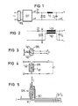
- the basic circuit diagram of a switched-mode power supply shown in FIG. 1 shows on the input side a line rectifier NGL with subsequent switching stage SST, which generates a square-wave voltage from the direct voltage by chopping and converts it with the aid of a transformer.
- the filter circuit consists of a smoothing choke L G switched on along the one output line and of a smoothing capacitor C G located in the shunt arm.
- Such a sieve circuit has the disadvantage that the HF interference radiation caused by the switching stage SST and symbolized by lightning arrows is only sufficiently reduced in the choke branch. In the second output line leading to the negative pole, which contains no smoothing choke, the RF interference radiation reaches the output unhindered.
- both chokes L G1 , L G2 each consist of one turn and, moreover, both turns are passed through the coil core SPK in the same winding direction. This means that the currents I flowing from point A to the positive pole or from the negative pole to point B add up through the coil core SPK.
- FIG. 5 A structure which is particularly advantageous for high-power switching power supplies for the filter chokes according to FIGS. 3 and 4 is shown in FIG. 5. It shows in perspective Representation of a conductor track assigned to the choke L G1 in the form of a copper strip.
- This copper strip is subdivided into three partial webs connected at one end, of which the middle partial web is guided as the first turn W1 through the bore of a tubular coil core SPK, while the two outer partial webs are returned on the outside of the core.
- These two outer partial tracks are extended beyond the core and, with their extended ends bent at right angles to the core axis, are connected to one of the two output terminals - here with the positive pole.
- the beginning of the middle partial web is also bent at right angles to the core axis and preferably in the opposite direction to the two outer partial webs.
- the conductor track assigned to the other choke L G2 is likewise a copper strip and, starting from the second output terminal, runs first between the two outer partial tracks of the other choke L G1 and then as a second turn W2 through the coil core SPK.
- the bent ends of the two outer sub-paths of inductor L G1 and the intermediate conductor path of inductor L G2 serve expediently as mounting surfaces for one or more smoothing capacitors C G connected in parallel.
Landscapes
- Engineering & Computer Science (AREA)
- Power Engineering (AREA)
- Power Conversion In General (AREA)
- Dc-Dc Converters (AREA)
- Filters And Equalizers (AREA)
- Details Of Television Scanning (AREA)
Abstract
Die im Sekundärkreis des Leistungsübertragers nach einem Gleichrichterteil (D1, D2) vorgesehene Siebschaltung besteht aus zwei in den zu den beiden Ausgangsklemmen führenden Leitungen jeweils im Längszweig angeordneten Drosseln (LG1, LG2) und wenigstens einem Querkondensator (CG). Beide Drosseln (LG1, LG2) bestehen aus je einer als streifenförmige Leiterbahn ausgebildeten Windung, (W1, W2), wobei beide Windungen im gleichen Wicklungssinn durch einen gemeinsamen Magnetkern (SPK) geführt sind.The filter circuit provided in the secondary circuit of the power transformer after a rectifier part (D1, D2) consists of two chokes (LG1, LG2) arranged in the lines leading to the two output terminals and at least one transverse capacitor (CG). Both chokes (LG1, LG2) each consist of a turn designed as a strip-shaped conductor track (W1, W2), both turns being guided in the same winding direction by a common magnetic core (SPK).
Description
Die Erfindung betrifft ein Hochleistungs-Schaltnetzteil nach dem Oberbegriff des Patentanspruchs 1.The invention relates to a high-performance switching power supply according to the preamble of claim 1.
Schaltnetzteile haben gegenüber herkömmlichen Netzteilen den wesentlichen Vorteil, daß sie bei niedrigerem Gewicht und geringerem Volumen bei entsprechend geringerem Kostenaufwand einen höheren Wirkungsgrad haben. Dem stehen als Nachteile eine etwas kompliziertere Schalttechnik, eine stärkere HF-Störstrahlung und größere Schwierigkeiten bei der Glättung der Ausgangsspannung gegenüber.Switched-mode power supplies have the essential advantage over conventional power supplies that they have a higher degree of efficiency with a lower weight and a smaller volume at a correspondingly lower cost. This is offset by the disadvantages of a somewhat more complicated switching technology, stronger RF interference and greater difficulties in smoothing the output voltage.
Stärkere HF-Störungen treten insbesondere bei Schaltnetzteilen auf, die nur in einem der zu den beiden Ausgangsklemmen führenden Leitungen eine Siebdrossel aufweisen mit der Folge, daß die HF-Störung über die jeweils andere drosselfreie Leitung bis zum Verbraucher gelangt. Der Einbau zusätzlicher HF-Drosseln in die beiden Ausgangsleitungen, ggfs. in Verbindung mit Y-Entstörkondensatoren, ist zwar grundsätzlich möglich, bedingt aber bei Hochleitungsgeräten einen erheblichen Aufwand, weil diese HF-Drosseln wegen ihrer Größe sehr teuer sind.Stronger HF interference occurs in particular in the case of switched-mode power supplies which have a filter choke only in one of the lines leading to the two output terminals, with the result that the HF interference reaches the consumer via the respective other choke-free line. The installation of additional RF chokes in the two output lines, possibly in conjunction with Y interference suppression capacitors, is in principle possible, but it requires considerable effort in high-line devices because these RF chokes are very expensive due to their size.
Dies gilt auch für den Fall, daß in jeder der beiden Ausgangsleitungen eine Leistungsdrossel zwischengeschaltet wird, weil die zweite Leistungsdrossel zwangsläufig einen zusätzlichen Raumbedarf und entsprechende Mehrkosten erfordert. Bei Hochleistungs-Schaltnetzteilen kommt erschwerend hinzu, daß Leistungsdrosseln wegen des großen Leitungsquerschnitts praktisch nicht "bewickelt" werden können.This also applies in the event that a power choke is interposed in each of the two output lines because the second power choke inevitably requires additional space and corresponding additional costs. In the case of high-performance switched-mode power supplies, this is made more difficult by the fact that power chokes can practically not be “wound” because of the large line cross section.
Der vorliegenden Erfindung liegt nun die Aufgabe zugrunde, für die Verbesserung der Glättung und HF-Entstörung bei Hochleistungs-Schaltkreisen eine auch im Hinblick auf den notwendigen Raum- und Materialbedarf möglichst optimale Lösung zu finden.The present invention is based on the object of finding a solution that is as optimal as possible also with regard to the necessary space and material requirements for improving smoothing and RF interference suppression in high-performance circuits.
Diese Aufgabe wird erfindungsgemäß durch die kennzeichnenden Merkmale des Patentanspruches 1 gelöst. Die erfindungsgemäße Anordnung entspricht einer Drossel mit zwei Windungen, ohne daß das Wicklungsmaterial mit seinem wegen der hohen Stromstärken entsprechend großen Querschnitt gewickelt werden muß. Ein weiterer Vorteil sind die aufgrund des symmetrischen Aufbaus guten Entstöreigenschaften der Siebschaltung.This object is achieved by the characterizing features of claim 1. The arrangement according to the invention corresponds to a choke with two turns, without the winding material having to be wound with its correspondingly large cross section because of the high current strengths. Another advantage is the good suppression properties of the filter circuit due to the symmetrical structure.
Vorteilhafte Weiterbildungen des Erfindungsgedankens ergeben sich durch die Merkmale der Unteransprüche.Advantageous developments of the inventive concept result from the features of the subclaims.
Im folgenden wird ein Ausführungsbeispiel der Erfindung anhand der Zeichnung näher erläutert. Dabei zeigen:
- FIG 1 das Prinzipschaltbild eines Schaltnetzteils mit einem im Ausgangskreis vorgesehenen LC-Siebglied
- FIG 2 eine Siebschaltung gemäß der Erfindung mit zwei Siebdrosseln
- FIG 3, 4 den prinzipiellen Aufbau einer Siebdrosselanordnung nach Fig. 2
- FIG 5 eine vorteilhafte Realisierung einer Siebdrosselanordnung nach den Fig. 3 und 4.
- 1 shows the basic circuit diagram of a switching power supply with an LC filter element provided in the output circuit
- 2 shows a screen circuit according to the invention with two screen chokes
- 3, 4 the basic structure of a screen throttle arrangement according to FIG. 2nd
- 5 shows an advantageous realization of a screen throttle arrangement according to FIGS. 3 and 4.
Das in Fig. 1 dargestellte Prinzipschaltbild eines Schaltnetzteils zeigt eingangsseitig einen Netzgleichrichter NGL mit nachfolgender Schaltstufe SST, die aus der Gleichspannung durch Zerhacken eine Rechteckspannung erzeugt und diese mit Hilfe eines Transformators übersetzt. Auf der Sekundärseite des Transformators, der gleichzeitig für eine Netztrennung sorgt, erfolgt zunächst eine Gleichrichtung mit Hilfe der beiden Gleichrichter D1, D2 und anschließend eine Siebung. Die Siebschaltung besteht aus einer längs der einen Ausgangsleitung eingeschalteten Glättungsdrossel LG und aus einem im Querzweig liegenden Glättungskondensators CG. Eine derartige Siebschaltung hat den Nachteil, daß die durch die Schaltstufe SST verursachte und durch Blitzpfeile symbolisierte HF-Störstrahlung nur im Drosselzweig ausreichend reduziert wird. In der zweiten, zum Minuspol führenden Ausgangsleitung, die keine Glättungsdrossel enthält, gelangt die HF-Störstrahlung nämlich ungehindert bis zum Ausgang.The basic circuit diagram of a switched-mode power supply shown in FIG. 1 shows on the input side a line rectifier NGL with subsequent switching stage SST, which generates a square-wave voltage from the direct voltage by chopping and converts it with the aid of a transformer. On the secondary side of the transformer, which at the same time ensures mains separation, rectification takes place with the aid of the two rectifiers D1, D2 and then screening. The filter circuit consists of a smoothing choke L G switched on along the one output line and of a smoothing capacitor C G located in the shunt arm. Such a sieve circuit has the disadvantage that the HF interference radiation caused by the switching stage SST and symbolized by lightning arrows is only sufficiently reduced in the choke branch. In the second output line leading to the negative pole, which contains no smoothing choke, the RF interference radiation reaches the output unhindered.
Die Siebschaltung nach Fig. 2 begegnet diesen Schwierigkeiten in vorteilhafter Weise dadurch, daß nun in beiden Ausgangsleitungen je eine Glättungsdrossel LG1, LG2 enthalten ist und daß beide Drosseln auf einem gemeinsamen Spulenkern angeordnet sind.2 meets these difficulties in an advantageous manner in that a smoothing choke L G1 , L G2 is now contained in each of the two output lines and in that both chokes are arranged on a common coil core.
Wie der in den Fig. 3 und 4 dargestellte Spulenaufbau zeigt, bestehen beide Drosseln LG1, LG2 aus je einer Windung und außerdem sind beide Windungen in gleichem Wicklungssinn durch den Spulenkern SPK geführt. Dies bedeutet, daß sich die vom Punkt A zum Pluspol bzw. vom Minuspol zum Punkt B jeweils durch den Spulenkern SPK fließenden Ströme I addieren.As the coil structure shown in FIGS. 3 and 4 shows, both chokes L G1 , L G2 each consist of one turn and, moreover, both turns are passed through the coil core SPK in the same winding direction. This means that the currents I flowing from point A to the positive pole or from the negative pole to point B add up through the coil core SPK.
Ein für Hochleistungs-Schaltnetzteile besonders vorteilhafter Aufbau für die Siebdrosseln nach den Fig. 3 und 4 ist in Fig. 5 dargestellt. Sie zeigt in perspektivischer Darstellung eine der Drossel LG1 zugeordnete Leiterbahn in Form eines Kupferbandes. Dieses Kupferband ist in drei an einem Ende zusammenhängende Teilbahnen unterteilt, von denen die mittlere Teilbahn als erste Windung W1 durch die Bohrung eines rohrförmigen Spulenkerns SPK geführt ist, während die beiden äußeren Teilbahnen außen am Kern zurückgeführt sind. Diese beiden äußeren Teilbahnen sind über den Kern hinaus verlängert und mit ihren verlängerten rechtwinkelig zur Kernachse abgebogenen Enden mit einer der beiden Ausgangsklemmen - hier mit dem Pluspol -verbunden. Der Anfang der mittleren Teilbahn ist ebenfalls rechtwinkelig zur Kernachse und zwar vorzugsweise in entgegengesetzter Richtung zu den beiden äußeren Teilbahnen abgebogen.A structure which is particularly advantageous for high-power switching power supplies for the filter chokes according to FIGS. 3 and 4 is shown in FIG. 5. It shows in perspective Representation of a conductor track assigned to the choke L G1 in the form of a copper strip. This copper strip is subdivided into three partial webs connected at one end, of which the middle partial web is guided as the first turn W1 through the bore of a tubular coil core SPK, while the two outer partial webs are returned on the outside of the core. These two outer partial tracks are extended beyond the core and, with their extended ends bent at right angles to the core axis, are connected to one of the two output terminals - here with the positive pole. The beginning of the middle partial web is also bent at right angles to the core axis and preferably in the opposite direction to the two outer partial webs.
Die der anderen Drossel LG2 zugeordnete Leiterbahn ist ebenfalls ein Kupferband und verläuft zunächst, ausgehend von der zweiten Ausgangsklemme, zwischen den beiden äußeren Teilbahnen der anderen Drossel LG1 und anschließend als zweite Windung W2 durch den Spulenkern SPK. Die abgebogenen Enden der beiden äußeren Teilbahnen von Drossel LG1 und die dazwischen liegende Leiterbahn von Drossel LG2 dienen zweckmäßig als Montageflächen für einen oder mehrere parallel geschaltete Glättungskondensatoren CG.The conductor track assigned to the other choke L G2 is likewise a copper strip and, starting from the second output terminal, runs first between the two outer partial tracks of the other choke L G1 and then as a second turn W2 through the coil core SPK. The bent ends of the two outer sub-paths of inductor L G1 and the intermediate conductor path of inductor L G2 serve expediently as mounting surfaces for one or more smoothing capacitors C G connected in parallel.
-
FIG 1 (Stand der Technik)
NGL Netzgleichrichter
SST Schaltstufe
D1, D2 Gleichrichter
LG Glättungsdrossel
CG Glättungskondensator
FIG 1 (prior art)
NGL line rectifier
SST switching stage
D1, D2 rectifiers
L G smoothing choke
C G smoothing capacitor
-
FIG 2 - 5
LG1,LG2 Glättungsdrossel
SPK Spulenkern
A, B Anschlüsse für LG1, LG2
Wl, W2 Windungen der Glättungsdrosseln L1, LG2
I StromFIG 2-5
L G1 , L G2 smoothing choke
SPK core
A, B connections for L G1 , L G2
Wl, W2 turns of smoothing chokes L 1 , L G2
I current
Claims (4)
dadurch gekennzeichnet, daß die beiden Drosseln (LG1, LG2) aus je einer als streifenförmige Leiterbahn ausgebildeten Windung (W1, W2) bestehen und daß beide Windungen (W1, W2) in gleichem Wicklungssinn durch einen gemeinsamen Magnetkern (SPK) geführt sind.1.High-performance switched-mode power supply with a power transformer, the primary branch of which consists of a mains rectifier and a switching stage, in the secondary circuit of which a filter circuit is provided after a rectifier part, which consists of two chokes arranged in the longitudinal branch in the lines leading to the two output terminals and at least one transverse capacitor consists,
characterized in that the two chokes (L G1 , L G2 ) each consist of a winding (W1, W2) formed as a strip-shaped conductor track and that both windings (W1, W2) are guided in the same winding direction by a common magnetic core (SPK).
dadurch gekennzeichnet, daß die Windung (W1) der einen Drossel (LG1) aus einer in drei Teilbahnen unterteilten Leiterbahn besteht, von denen die mittlere Leiterbahn durch den Magnetkern (SPK) geführt und die beiden äußeren Teilbahnen außen am Kern zurückgeführt und mit einer der beiden Ausgangsklemmen verbunden sind.2. High-performance switching power supply according to claim 1,
characterized in that the winding (W1) of the one choke (L G1 ) consists of a conductor track subdivided into three partial tracks, of which the middle conductor track is guided through the magnetic core (SPK) and the two outer partial tracks are returned outside the core and with one of the two output terminals are connected.
dadurch gekennzeichnet, daß die mit der anderen Ausgangsklemme verbundene Leiterbahn der anderen Drossel (LG2) zwischen den beiden Teilbahnen der einen Drossel (LG1) und anschließend durch den Magnetkern (SPK) geführt ist.3. High-performance switching power supply according to claim 2,
characterized in that the conductor track of the other choke (L G2 ) connected to the other output terminal is guided between the two partial tracks of the one choke (L G1 ) and then through the magnetic core (SPK).
dadurch gekennzeichnet, daß die verlängerten Enden der beiden äußeren Teilbahnen der einen Drossel (LG1) und der zwischen diesen beiden Teilbahnen verlaufende Abschnitt der Leiterbahn für die andere Drossel (LG2) als Montageflache für einen oder mehrere parallel geschaltete Glättungskondensatoren (CG) dient.4. High-performance switching power supply according to claims 2 and 3,
characterized in that the Extended ends of the two outer partial tracks of a choke (L G1 ) and the section of the conductor track running between these two partial tracks for the other choke (L G2 ) serves as a mounting surface for one or more smoothing capacitors (C G ) connected in parallel.
Priority Applications (1)
| Application Number | Priority Date | Filing Date | Title |
|---|---|---|---|
| AT87102636T ATE80493T1 (en) | 1986-02-28 | 1987-02-25 | CHOKE FOR HIGH-PERFORMANCE SWITCHING POWER SUPPLY. |
Applications Claiming Priority (2)
| Application Number | Priority Date | Filing Date | Title |
|---|---|---|---|
| DE3606592 | 1986-02-28 | ||
| DE3606592 | 1986-02-28 |
Publications (3)
| Publication Number | Publication Date |
|---|---|
| EP0239786A2 true EP0239786A2 (en) | 1987-10-07 |
| EP0239786A3 EP0239786A3 (en) | 1988-10-12 |
| EP0239786B1 EP0239786B1 (en) | 1992-09-09 |
Family
ID=6295208
Family Applications (1)
| Application Number | Title | Priority Date | Filing Date |
|---|---|---|---|
| EP87102636A Expired - Lifetime EP0239786B1 (en) | 1986-02-28 | 1987-02-25 | Choke for a high power switching power supply |
Country Status (5)
| Country | Link |
|---|---|
| US (1) | US4791543A (en) |
| EP (1) | EP0239786B1 (en) |
| AT (1) | ATE80493T1 (en) |
| DE (1) | DE3781578D1 (en) |
| ES (1) | ES2033704T3 (en) |
Cited By (3)
| Publication number | Priority date | Publication date | Assignee | Title |
|---|---|---|---|---|
| GB2243258A (en) * | 1990-04-20 | 1991-10-23 | Gold Star Co | Magnetron for microwave oven |
| US5493471A (en) * | 1992-07-04 | 1996-02-20 | Abb Patent Gmbh | Output capacitor array of a switched-mode power supply |
| DE102005037616A1 (en) * | 2005-08-09 | 2007-02-15 | Rohde & Schwarz Gmbh & Co. Kg | Line transformer for impedance matching |
Families Citing this family (2)
| Publication number | Priority date | Publication date | Assignee | Title |
|---|---|---|---|---|
| SE464001B (en) * | 1989-06-20 | 1991-02-18 | Ericsson Telefon Ab L M | GLOVING FILTER PUTS A RECTIFIER |
| US6874708B2 (en) * | 2003-02-13 | 2005-04-05 | Illinois Tool Works Inc. | Automatic air-assisted manifold mounted gun |
Citations (1)
| Publication number | Priority date | Publication date | Assignee | Title |
|---|---|---|---|---|
| DE486189C (en) * | 1929-11-12 | Siemens Schuckertwerke Akt Ges | In the course of the forward and backward transmission of strong currents, there is a choke coil to increase the inductive voltage drop |
Family Cites Families (6)
| Publication number | Priority date | Publication date | Assignee | Title |
|---|---|---|---|---|
| US3340458A (en) * | 1964-06-16 | 1967-09-05 | Roy M Keller | Filter choke with self-desaturating magnetic core |
| FR1422994A (en) * | 1964-11-17 | 1966-01-03 | Simple rectifier circuit providing two symmetrical DC voltages | |
| US3611233A (en) * | 1969-08-14 | 1971-10-05 | Atomic Energy Commission | Pulse transformer using stripline windings |
| US3916286A (en) * | 1974-09-19 | 1975-10-28 | United Technologies Corp | Switching power supply common output filter |
| SU982163A1 (en) * | 1981-03-24 | 1982-12-15 | Предприятие П/Я В-8466 | Converter |
| US4586120A (en) * | 1983-12-30 | 1986-04-29 | At&T Bell Laboratories | Current limit shutdown circuit with time delay |
-
1987
- 1987-02-25 AT AT87102636T patent/ATE80493T1/en not_active IP Right Cessation
- 1987-02-25 ES ES198787102636T patent/ES2033704T3/en not_active Expired - Lifetime
- 1987-02-25 DE DE8787102636T patent/DE3781578D1/en not_active Expired - Fee Related
- 1987-02-25 EP EP87102636A patent/EP0239786B1/en not_active Expired - Lifetime
-
1988
- 1988-03-03 US US07/168,592 patent/US4791543A/en not_active Expired - Fee Related
Patent Citations (1)
| Publication number | Priority date | Publication date | Assignee | Title |
|---|---|---|---|---|
| DE486189C (en) * | 1929-11-12 | Siemens Schuckertwerke Akt Ges | In the course of the forward and backward transmission of strong currents, there is a choke coil to increase the inductive voltage drop |
Non-Patent Citations (1)
| Title |
|---|
| ELEKTRONIK, Band 34, Nr. 15, Juli 1985, Seiten 94-96, M}nchen; H. PANSE "Verringerung der Restwelligkeit bei Schaltnetzteilen" * |
Cited By (4)
| Publication number | Priority date | Publication date | Assignee | Title |
|---|---|---|---|---|
| GB2243258A (en) * | 1990-04-20 | 1991-10-23 | Gold Star Co | Magnetron for microwave oven |
| GB2243258B (en) * | 1990-04-20 | 1994-09-07 | Gold Star Co | Magnetron for microwave oven |
| US5493471A (en) * | 1992-07-04 | 1996-02-20 | Abb Patent Gmbh | Output capacitor array of a switched-mode power supply |
| DE102005037616A1 (en) * | 2005-08-09 | 2007-02-15 | Rohde & Schwarz Gmbh & Co. Kg | Line transformer for impedance matching |
Also Published As
| Publication number | Publication date |
|---|---|
| ES2033704T3 (en) | 1993-04-01 |
| EP0239786A3 (en) | 1988-10-12 |
| EP0239786B1 (en) | 1992-09-09 |
| DE3781578D1 (en) | 1992-10-15 |
| US4791543A (en) | 1988-12-13 |
| ATE80493T1 (en) | 1992-09-15 |
Similar Documents
| Publication | Publication Date | Title |
|---|---|---|
| DE3325612C2 (en) | ||
| DE102006014608B4 (en) | Filter circuit and power supply unit | |
| DE3039530C2 (en) | ||
| DE2950411A1 (en) | RECTIFIER DEVICE WITH SCREENED OUTPUT VOLTAGE | |
| DE19906261A1 (en) | Sheet transformer | |
| DE19901930A1 (en) | Combinational circuit component | |
| DE102016201258A1 (en) | Electric voltage converter with several storage chokes | |
| EP0239786B1 (en) | Choke for a high power switching power supply | |
| EP1076406B1 (en) | Half bridge inverter | |
| WO2014001116A1 (en) | Parallel inverter on a choke | |
| DE19829424A1 (en) | Unipolar filter for reducing zero currents in electric power supply | |
| DE102004008961B4 (en) | Coil body for closed magnetic core, has guiding units arranged outside supporting surface, winding space defined between units and under windings, and separating units designed as flat ledges | |
| CH491526A (en) | Electric rectifier system | |
| EP0082966B1 (en) | Line transformer for television receivers | |
| EP2863402A1 (en) | Strip winding for high voltage transformers | |
| EP0066803A2 (en) | Line transformer for television receivers | |
| DE3635365A1 (en) | SECONDARY SWITCHABLE POWER SUPPLY | |
| DE3039549A1 (en) | Small size electrical transformer - has spiral insulator between primary and secondary coils to simplify manufacture | |
| DE2418230B2 (en) | Capacitively controlled high-voltage winding made of disc coils for transformers with high outputs | |
| DE3342011C2 (en) | Low pass filter for electrical consumers | |
| DE2420451C2 (en) | Device for doubling the tension | |
| DE2320589A1 (en) | TRANSFORMER WITH WINDING CORE | |
| DE69925973T2 (en) | Line filter | |
| DE2625165A1 (en) | TRANSFORMER COIL FOR VERY HIGH VOLTAGE | |
| DE4307607C2 (en) | Circuit arrangement for uniform current distribution when connecting partial rectifier groups in parallel |
Legal Events
| Date | Code | Title | Description |
|---|---|---|---|
| PUAI | Public reference made under article 153(3) epc to a published international application that has entered the european phase |
Free format text: ORIGINAL CODE: 0009012 |
|
| AK | Designated contracting states |
Kind code of ref document: A2 Designated state(s): AT BE CH DE ES FR GB GR IT LI NL SE |
|
| PUAL | Search report despatched |
Free format text: ORIGINAL CODE: 0009013 |
|
| AK | Designated contracting states |
Kind code of ref document: A3 Designated state(s): AT BE CH DE ES FR GB GR IT LI NL SE |
|
| 17P | Request for examination filed |
Effective date: 19881108 |
|
| 17Q | First examination report despatched |
Effective date: 19901212 |
|
| RAP1 | Party data changed (applicant data changed or rights of an application transferred) |
Owner name: SIEMENS NIXDORF INFORMATIONSSYSTEME AG |
|
| GRAA | (expected) grant |
Free format text: ORIGINAL CODE: 0009210 |
|
| AK | Designated contracting states |
Kind code of ref document: B1 Designated state(s): AT BE CH DE ES FR GB GR IT LI NL SE |
|
| PG25 | Lapsed in a contracting state [announced via postgrant information from national office to epo] |
Ref country code: GR Free format text: LAPSE BECAUSE OF FAILURE TO SUBMIT A TRANSLATION OF THE DESCRIPTION OR TO PAY THE FEE WITHIN THE PRESCRIBED TIME-LIMIT Effective date: 19920909 |
|
| REF | Corresponds to: |
Ref document number: 80493 Country of ref document: AT Date of ref document: 19920915 Kind code of ref document: T |
|
| REF | Corresponds to: |
Ref document number: 3781578 Country of ref document: DE Date of ref document: 19921015 |
|
| ET | Fr: translation filed | ||
| ITF | It: translation for a ep patent filed |
Owner name: STUDIO JAUMANN |
|
| GBT | Gb: translation of ep patent filed (gb section 77(6)(a)/1977) | ||
| PG25 | Lapsed in a contracting state [announced via postgrant information from national office to epo] |
Ref country code: GB Effective date: 19930225 Ref country code: AT Effective date: 19930225 |
|
| PG25 | Lapsed in a contracting state [announced via postgrant information from national office to epo] |
Ref country code: SE Effective date: 19930226 Ref country code: ES Free format text: LAPSE BECAUSE OF NON-PAYMENT OF DUE FEES Effective date: 19930226 |
|
| PG25 | Lapsed in a contracting state [announced via postgrant information from national office to epo] |
Ref country code: LI Effective date: 19930228 Ref country code: CH Effective date: 19930228 Ref country code: BE Effective date: 19930228 |
|
| REG | Reference to a national code |
Ref country code: ES Ref legal event code: FG2A Ref document number: 2033704 Country of ref document: ES Kind code of ref document: T3 |
|
| PLBE | No opposition filed within time limit |
Free format text: ORIGINAL CODE: 0009261 |
|
| STAA | Information on the status of an ep patent application or granted ep patent |
Free format text: STATUS: NO OPPOSITION FILED WITHIN TIME LIMIT |
|
| BERE | Be: lapsed |
Owner name: SIEMENS NIXDORF INFORMATIONSSYSTEME A.G. Effective date: 19930228 |
|
| 26N | No opposition filed | ||
| PG25 | Lapsed in a contracting state [announced via postgrant information from national office to epo] |
Ref country code: NL Effective date: 19930901 |
|
| NLV4 | Nl: lapsed or anulled due to non-payment of the annual fee | ||
| GBPC | Gb: european patent ceased through non-payment of renewal fee |
Effective date: 19930225 |
|
| PG25 | Lapsed in a contracting state [announced via postgrant information from national office to epo] |
Ref country code: FR Effective date: 19931029 |
|
| REG | Reference to a national code |
Ref country code: CH Ref legal event code: PL |
|
| PG25 | Lapsed in a contracting state [announced via postgrant information from national office to epo] |
Ref country code: DE Effective date: 19931103 |
|
| REG | Reference to a national code |
Ref country code: FR Ref legal event code: ST |
|
| EUG | Se: european patent has lapsed |
Ref document number: 87102636.5 Effective date: 19930912 |
|
| REG | Reference to a national code |
Ref country code: ES Ref legal event code: FD2A Effective date: 19990201 |
|
| PG25 | Lapsed in a contracting state [announced via postgrant information from national office to epo] |
Ref country code: IT Free format text: LAPSE BECAUSE OF NON-PAYMENT OF DUE FEES;WARNING: LAPSES OF ITALIAN PATENTS WITH EFFECTIVE DATE BEFORE 2007 MAY HAVE OCCURRED AT ANY TIME BEFORE 2007. THE CORRECT EFFECTIVE DATE MAY BE DIFFERENT FROM THE ONE RECORDED. Effective date: 20050225 |