EP0240433A2 - Single bonding shelf, multi-row, wire-bond finger layout for integrated circuit package - Google Patents
Single bonding shelf, multi-row, wire-bond finger layout for integrated circuit package Download PDFInfo
- Publication number
- EP0240433A2 EP0240433A2 EP87400729A EP87400729A EP0240433A2 EP 0240433 A2 EP0240433 A2 EP 0240433A2 EP 87400729 A EP87400729 A EP 87400729A EP 87400729 A EP87400729 A EP 87400729A EP 0240433 A2 EP0240433 A2 EP 0240433A2
- Authority
- EP
- European Patent Office
- Prior art keywords
- bonding
- package
- pads
- conductive
- conductive path
- Prior art date
- Legal status (The legal status is an assumption and is not a legal conclusion. Google has not performed a legal analysis and makes no representation as to the accuracy of the status listed.)
- Withdrawn
Links
Images
Classifications
-
- H—ELECTRICITY
- H01—ELECTRIC ELEMENTS
- H01L—SEMICONDUCTOR DEVICES NOT COVERED BY CLASS H10
- H01L23/00—Details of semiconductor or other solid state devices
- H01L23/48—Arrangements for conducting electric current to or from the solid state body in operation, e.g. leads, terminal arrangements ; Selection of materials therefor
- H01L23/488—Arrangements for conducting electric current to or from the solid state body in operation, e.g. leads, terminal arrangements ; Selection of materials therefor consisting of soldered or bonded constructions
- H01L23/498—Leads, i.e. metallisations or lead-frames on insulating substrates, e.g. chip carriers
- H01L23/49822—Multilayer substrates
-
- H—ELECTRICITY
- H01—ELECTRIC ELEMENTS
- H01L—SEMICONDUCTOR DEVICES NOT COVERED BY CLASS H10
- H01L24/00—Arrangements for connecting or disconnecting semiconductor or solid-state bodies; Methods or apparatus related thereto
- H01L24/01—Means for bonding being attached to, or being formed on, the surface to be connected, e.g. chip-to-package, die-attach, "first-level" interconnects; Manufacturing methods related thereto
- H01L24/26—Layer connectors, e.g. plate connectors, solder or adhesive layers; Manufacturing methods related thereto
- H01L24/28—Structure, shape, material or disposition of the layer connectors prior to the connecting process
- H01L24/29—Structure, shape, material or disposition of the layer connectors prior to the connecting process of an individual layer connector
-
- H—ELECTRICITY
- H01—ELECTRIC ELEMENTS
- H01L—SEMICONDUCTOR DEVICES NOT COVERED BY CLASS H10
- H01L24/00—Arrangements for connecting or disconnecting semiconductor or solid-state bodies; Methods or apparatus related thereto
- H01L24/01—Means for bonding being attached to, or being formed on, the surface to be connected, e.g. chip-to-package, die-attach, "first-level" interconnects; Manufacturing methods related thereto
- H01L24/42—Wire connectors; Manufacturing methods related thereto
- H01L24/47—Structure, shape, material or disposition of the wire connectors after the connecting process
- H01L24/49—Structure, shape, material or disposition of the wire connectors after the connecting process of a plurality of wire connectors
-
- H—ELECTRICITY
- H01—ELECTRIC ELEMENTS
- H01L—SEMICONDUCTOR DEVICES NOT COVERED BY CLASS H10
- H01L2223/00—Details relating to semiconductor or other solid state devices covered by the group H01L23/00
- H01L2223/544—Marks applied to semiconductor devices or parts
- H01L2223/5442—Marks applied to semiconductor devices or parts comprising non digital, non alphanumeric information, e.g. symbols
-
- H—ELECTRICITY
- H01—ELECTRIC ELEMENTS
- H01L—SEMICONDUCTOR DEVICES NOT COVERED BY CLASS H10
- H01L2223/00—Details relating to semiconductor or other solid state devices covered by the group H01L23/00
- H01L2223/544—Marks applied to semiconductor devices or parts
- H01L2223/54426—Marks applied to semiconductor devices or parts for alignment
-
- H—ELECTRICITY
- H01—ELECTRIC ELEMENTS
- H01L—SEMICONDUCTOR DEVICES NOT COVERED BY CLASS H10
- H01L2223/00—Details relating to semiconductor or other solid state devices covered by the group H01L23/00
- H01L2223/544—Marks applied to semiconductor devices or parts
- H01L2223/54473—Marks applied to semiconductor devices or parts for use after dicing
-
- H—ELECTRICITY
- H01—ELECTRIC ELEMENTS
- H01L—SEMICONDUCTOR DEVICES NOT COVERED BY CLASS H10
- H01L2224/00—Indexing scheme for arrangements for connecting or disconnecting semiconductor or solid-state bodies and methods related thereto as covered by H01L24/00
- H01L2224/01—Means for bonding being attached to, or being formed on, the surface to be connected, e.g. chip-to-package, die-attach, "first-level" interconnects; Manufacturing methods related thereto
- H01L2224/02—Bonding areas; Manufacturing methods related thereto
- H01L2224/04—Structure, shape, material or disposition of the bonding areas prior to the connecting process
- H01L2224/05—Structure, shape, material or disposition of the bonding areas prior to the connecting process of an individual bonding area
- H01L2224/0554—External layer
- H01L2224/0555—Shape
- H01L2224/05552—Shape in top view
- H01L2224/05554—Shape in top view being square
-
- H—ELECTRICITY
- H01—ELECTRIC ELEMENTS
- H01L—SEMICONDUCTOR DEVICES NOT COVERED BY CLASS H10
- H01L2224/00—Indexing scheme for arrangements for connecting or disconnecting semiconductor or solid-state bodies and methods related thereto as covered by H01L24/00
- H01L2224/01—Means for bonding being attached to, or being formed on, the surface to be connected, e.g. chip-to-package, die-attach, "first-level" interconnects; Manufacturing methods related thereto
- H01L2224/26—Layer connectors, e.g. plate connectors, solder or adhesive layers; Manufacturing methods related thereto
- H01L2224/28—Structure, shape, material or disposition of the layer connectors prior to the connecting process
- H01L2224/29—Structure, shape, material or disposition of the layer connectors prior to the connecting process of an individual layer connector
- H01L2224/29001—Core members of the layer connector
- H01L2224/29099—Material
- H01L2224/291—Material with a principal constituent of the material being a metal or a metalloid, e.g. boron [B], silicon [Si], germanium [Ge], arsenic [As], antimony [Sb], tellurium [Te] and polonium [Po], and alloys thereof
- H01L2224/29138—Material with a principal constituent of the material being a metal or a metalloid, e.g. boron [B], silicon [Si], germanium [Ge], arsenic [As], antimony [Sb], tellurium [Te] and polonium [Po], and alloys thereof the principal constituent melting at a temperature of greater than or equal to 950°C and less than 1550°C
- H01L2224/29144—Gold [Au] as principal constituent
-
- H—ELECTRICITY
- H01—ELECTRIC ELEMENTS
- H01L—SEMICONDUCTOR DEVICES NOT COVERED BY CLASS H10
- H01L2224/00—Indexing scheme for arrangements for connecting or disconnecting semiconductor or solid-state bodies and methods related thereto as covered by H01L24/00
- H01L2224/01—Means for bonding being attached to, or being formed on, the surface to be connected, e.g. chip-to-package, die-attach, "first-level" interconnects; Manufacturing methods related thereto
- H01L2224/26—Layer connectors, e.g. plate connectors, solder or adhesive layers; Manufacturing methods related thereto
- H01L2224/31—Structure, shape, material or disposition of the layer connectors after the connecting process
- H01L2224/32—Structure, shape, material or disposition of the layer connectors after the connecting process of an individual layer connector
- H01L2224/325—Material
- H01L2224/32505—Material outside the bonding interface, e.g. in the bulk of the layer connector
- H01L2224/32506—Material outside the bonding interface, e.g. in the bulk of the layer connector comprising an eutectic alloy
-
- H—ELECTRICITY
- H01—ELECTRIC ELEMENTS
- H01L—SEMICONDUCTOR DEVICES NOT COVERED BY CLASS H10
- H01L2224/00—Indexing scheme for arrangements for connecting or disconnecting semiconductor or solid-state bodies and methods related thereto as covered by H01L24/00
- H01L2224/01—Means for bonding being attached to, or being formed on, the surface to be connected, e.g. chip-to-package, die-attach, "first-level" interconnects; Manufacturing methods related thereto
- H01L2224/42—Wire connectors; Manufacturing methods related thereto
- H01L2224/47—Structure, shape, material or disposition of the wire connectors after the connecting process
- H01L2224/48—Structure, shape, material or disposition of the wire connectors after the connecting process of an individual wire connector
- H01L2224/4805—Shape
- H01L2224/4809—Loop shape
- H01L2224/48091—Arched
-
- H—ELECTRICITY
- H01—ELECTRIC ELEMENTS
- H01L—SEMICONDUCTOR DEVICES NOT COVERED BY CLASS H10
- H01L2224/00—Indexing scheme for arrangements for connecting or disconnecting semiconductor or solid-state bodies and methods related thereto as covered by H01L24/00
- H01L2224/01—Means for bonding being attached to, or being formed on, the surface to be connected, e.g. chip-to-package, die-attach, "first-level" interconnects; Manufacturing methods related thereto
- H01L2224/42—Wire connectors; Manufacturing methods related thereto
- H01L2224/47—Structure, shape, material or disposition of the wire connectors after the connecting process
- H01L2224/48—Structure, shape, material or disposition of the wire connectors after the connecting process of an individual wire connector
- H01L2224/481—Disposition
- H01L2224/48151—Connecting between a semiconductor or solid-state body and an item not being a semiconductor or solid-state body, e.g. chip-to-substrate, chip-to-passive
- H01L2224/48221—Connecting between a semiconductor or solid-state body and an item not being a semiconductor or solid-state body, e.g. chip-to-substrate, chip-to-passive the body and the item being stacked
- H01L2224/48225—Connecting between a semiconductor or solid-state body and an item not being a semiconductor or solid-state body, e.g. chip-to-substrate, chip-to-passive the body and the item being stacked the item being non-metallic, e.g. insulating substrate with or without metallisation
- H01L2224/48227—Connecting between a semiconductor or solid-state body and an item not being a semiconductor or solid-state body, e.g. chip-to-substrate, chip-to-passive the body and the item being stacked the item being non-metallic, e.g. insulating substrate with or without metallisation connecting the wire to a bond pad of the item
-
- H—ELECTRICITY
- H01—ELECTRIC ELEMENTS
- H01L—SEMICONDUCTOR DEVICES NOT COVERED BY CLASS H10
- H01L2224/00—Indexing scheme for arrangements for connecting or disconnecting semiconductor or solid-state bodies and methods related thereto as covered by H01L24/00
- H01L2224/01—Means for bonding being attached to, or being formed on, the surface to be connected, e.g. chip-to-package, die-attach, "first-level" interconnects; Manufacturing methods related thereto
- H01L2224/42—Wire connectors; Manufacturing methods related thereto
- H01L2224/47—Structure, shape, material or disposition of the wire connectors after the connecting process
- H01L2224/49—Structure, shape, material or disposition of the wire connectors after the connecting process of a plurality of wire connectors
- H01L2224/491—Disposition
- H01L2224/4912—Layout
- H01L2224/49175—Parallel arrangements
-
- H—ELECTRICITY
- H01—ELECTRIC ELEMENTS
- H01L—SEMICONDUCTOR DEVICES NOT COVERED BY CLASS H10
- H01L2224/00—Indexing scheme for arrangements for connecting or disconnecting semiconductor or solid-state bodies and methods related thereto as covered by H01L24/00
- H01L2224/01—Means for bonding being attached to, or being formed on, the surface to be connected, e.g. chip-to-package, die-attach, "first-level" interconnects; Manufacturing methods related thereto
- H01L2224/42—Wire connectors; Manufacturing methods related thereto
- H01L2224/47—Structure, shape, material or disposition of the wire connectors after the connecting process
- H01L2224/49—Structure, shape, material or disposition of the wire connectors after the connecting process of a plurality of wire connectors
- H01L2224/494—Connecting portions
- H01L2224/4943—Connecting portions the connecting portions being staggered
- H01L2224/49433—Connecting portions the connecting portions being staggered outside the semiconductor or solid-state body
-
- H—ELECTRICITY
- H01—ELECTRIC ELEMENTS
- H01L—SEMICONDUCTOR DEVICES NOT COVERED BY CLASS H10
- H01L2224/00—Indexing scheme for arrangements for connecting or disconnecting semiconductor or solid-state bodies and methods related thereto as covered by H01L24/00
- H01L2224/73—Means for bonding being of different types provided for in two or more of groups H01L2224/10, H01L2224/18, H01L2224/26, H01L2224/34, H01L2224/42, H01L2224/50, H01L2224/63, H01L2224/71
- H01L2224/732—Location after the connecting process
- H01L2224/73251—Location after the connecting process on different surfaces
- H01L2224/73265—Layer and wire connectors
-
- H—ELECTRICITY
- H01—ELECTRIC ELEMENTS
- H01L—SEMICONDUCTOR DEVICES NOT COVERED BY CLASS H10
- H01L2224/00—Indexing scheme for arrangements for connecting or disconnecting semiconductor or solid-state bodies and methods related thereto as covered by H01L24/00
- H01L2224/80—Methods for connecting semiconductor or other solid state bodies using means for bonding being attached to, or being formed on, the surface to be connected
- H01L2224/83—Methods for connecting semiconductor or other solid state bodies using means for bonding being attached to, or being formed on, the surface to be connected using a layer connector
- H01L2224/838—Bonding techniques
- H01L2224/83801—Soldering or alloying
- H01L2224/83805—Soldering or alloying involving forming a eutectic alloy at the bonding interface
-
- H—ELECTRICITY
- H01—ELECTRIC ELEMENTS
- H01L—SEMICONDUCTOR DEVICES NOT COVERED BY CLASS H10
- H01L24/00—Arrangements for connecting or disconnecting semiconductor or solid-state bodies; Methods or apparatus related thereto
- H01L24/01—Means for bonding being attached to, or being formed on, the surface to be connected, e.g. chip-to-package, die-attach, "first-level" interconnects; Manufacturing methods related thereto
- H01L24/42—Wire connectors; Manufacturing methods related thereto
- H01L24/47—Structure, shape, material or disposition of the wire connectors after the connecting process
- H01L24/48—Structure, shape, material or disposition of the wire connectors after the connecting process of an individual wire connector
-
- H—ELECTRICITY
- H01—ELECTRIC ELEMENTS
- H01L—SEMICONDUCTOR DEVICES NOT COVERED BY CLASS H10
- H01L2924/00—Indexing scheme for arrangements or methods for connecting or disconnecting semiconductor or solid-state bodies as covered by H01L24/00
- H01L2924/0001—Technical content checked by a classifier
- H01L2924/00014—Technical content checked by a classifier the subject-matter covered by the group, the symbol of which is combined with the symbol of this group, being disclosed without further technical details
-
- H—ELECTRICITY
- H01—ELECTRIC ELEMENTS
- H01L—SEMICONDUCTOR DEVICES NOT COVERED BY CLASS H10
- H01L2924/00—Indexing scheme for arrangements or methods for connecting or disconnecting semiconductor or solid-state bodies as covered by H01L24/00
- H01L2924/01—Chemical elements
- H01L2924/01006—Carbon [C]
-
- H—ELECTRICITY
- H01—ELECTRIC ELEMENTS
- H01L—SEMICONDUCTOR DEVICES NOT COVERED BY CLASS H10
- H01L2924/00—Indexing scheme for arrangements or methods for connecting or disconnecting semiconductor or solid-state bodies as covered by H01L24/00
- H01L2924/01—Chemical elements
- H01L2924/01013—Aluminum [Al]
-
- H—ELECTRICITY
- H01—ELECTRIC ELEMENTS
- H01L—SEMICONDUCTOR DEVICES NOT COVERED BY CLASS H10
- H01L2924/00—Indexing scheme for arrangements or methods for connecting or disconnecting semiconductor or solid-state bodies as covered by H01L24/00
- H01L2924/01—Chemical elements
- H01L2924/01014—Silicon [Si]
-
- H—ELECTRICITY
- H01—ELECTRIC ELEMENTS
- H01L—SEMICONDUCTOR DEVICES NOT COVERED BY CLASS H10
- H01L2924/00—Indexing scheme for arrangements or methods for connecting or disconnecting semiconductor or solid-state bodies as covered by H01L24/00
- H01L2924/01—Chemical elements
- H01L2924/01027—Cobalt [Co]
-
- H—ELECTRICITY
- H01—ELECTRIC ELEMENTS
- H01L—SEMICONDUCTOR DEVICES NOT COVERED BY CLASS H10
- H01L2924/00—Indexing scheme for arrangements or methods for connecting or disconnecting semiconductor or solid-state bodies as covered by H01L24/00
- H01L2924/01—Chemical elements
- H01L2924/01047—Silver [Ag]
-
- H—ELECTRICITY
- H01—ELECTRIC ELEMENTS
- H01L—SEMICONDUCTOR DEVICES NOT COVERED BY CLASS H10
- H01L2924/00—Indexing scheme for arrangements or methods for connecting or disconnecting semiconductor or solid-state bodies as covered by H01L24/00
- H01L2924/01—Chemical elements
- H01L2924/01074—Tungsten [W]
-
- H—ELECTRICITY
- H01—ELECTRIC ELEMENTS
- H01L—SEMICONDUCTOR DEVICES NOT COVERED BY CLASS H10
- H01L2924/00—Indexing scheme for arrangements or methods for connecting or disconnecting semiconductor or solid-state bodies as covered by H01L24/00
- H01L2924/01—Chemical elements
- H01L2924/01079—Gold [Au]
-
- H—ELECTRICITY
- H01—ELECTRIC ELEMENTS
- H01L—SEMICONDUCTOR DEVICES NOT COVERED BY CLASS H10
- H01L2924/00—Indexing scheme for arrangements or methods for connecting or disconnecting semiconductor or solid-state bodies as covered by H01L24/00
- H01L2924/013—Alloys
- H01L2924/0132—Binary Alloys
-
- H—ELECTRICITY
- H01—ELECTRIC ELEMENTS
- H01L—SEMICONDUCTOR DEVICES NOT COVERED BY CLASS H10
- H01L2924/00—Indexing scheme for arrangements or methods for connecting or disconnecting semiconductor or solid-state bodies as covered by H01L24/00
- H01L2924/013—Alloys
- H01L2924/0132—Binary Alloys
- H01L2924/01322—Eutectic Alloys, i.e. obtained by a liquid transforming into two solid phases
-
- H—ELECTRICITY
- H01—ELECTRIC ELEMENTS
- H01L—SEMICONDUCTOR DEVICES NOT COVERED BY CLASS H10
- H01L2924/00—Indexing scheme for arrangements or methods for connecting or disconnecting semiconductor or solid-state bodies as covered by H01L24/00
- H01L2924/013—Alloys
- H01L2924/014—Solder alloys
-
- H—ELECTRICITY
- H01—ELECTRIC ELEMENTS
- H01L—SEMICONDUCTOR DEVICES NOT COVERED BY CLASS H10
- H01L2924/00—Indexing scheme for arrangements or methods for connecting or disconnecting semiconductor or solid-state bodies as covered by H01L24/00
- H01L2924/095—Indexing scheme for arrangements or methods for connecting or disconnecting semiconductor or solid-state bodies as covered by H01L24/00 with a principal constituent of the material being a combination of two or more materials provided in the groups H01L2924/013 - H01L2924/0715
- H01L2924/097—Glass-ceramics, e.g. devitrified glass
- H01L2924/09701—Low temperature co-fired ceramic [LTCC]
-
- H—ELECTRICITY
- H01—ELECTRIC ELEMENTS
- H01L—SEMICONDUCTOR DEVICES NOT COVERED BY CLASS H10
- H01L2924/00—Indexing scheme for arrangements or methods for connecting or disconnecting semiconductor or solid-state bodies as covered by H01L24/00
- H01L2924/10—Details of semiconductor or other solid state devices to be connected
- H01L2924/102—Material of the semiconductor or solid state bodies
- H01L2924/1025—Semiconducting materials
- H01L2924/10251—Elemental semiconductors, i.e. Group IV
- H01L2924/10253—Silicon [Si]
-
- H—ELECTRICITY
- H01—ELECTRIC ELEMENTS
- H01L—SEMICONDUCTOR DEVICES NOT COVERED BY CLASS H10
- H01L2924/00—Indexing scheme for arrangements or methods for connecting or disconnecting semiconductor or solid-state bodies as covered by H01L24/00
- H01L2924/10—Details of semiconductor or other solid state devices to be connected
- H01L2924/11—Device type
- H01L2924/14—Integrated circuits
-
- H—ELECTRICITY
- H01—ELECTRIC ELEMENTS
- H01L—SEMICONDUCTOR DEVICES NOT COVERED BY CLASS H10
- H01L2924/00—Indexing scheme for arrangements or methods for connecting or disconnecting semiconductor or solid-state bodies as covered by H01L24/00
- H01L2924/15—Details of package parts other than the semiconductor or other solid state devices to be connected
- H01L2924/151—Die mounting substrate
- H01L2924/1515—Shape
- H01L2924/15153—Shape the die mounting substrate comprising a recess for hosting the device
-
- H—ELECTRICITY
- H01—ELECTRIC ELEMENTS
- H01L—SEMICONDUCTOR DEVICES NOT COVERED BY CLASS H10
- H01L2924/00—Indexing scheme for arrangements or methods for connecting or disconnecting semiconductor or solid-state bodies as covered by H01L24/00
- H01L2924/15—Details of package parts other than the semiconductor or other solid state devices to be connected
- H01L2924/151—Die mounting substrate
- H01L2924/15165—Monolayer substrate
-
- H—ELECTRICITY
- H01—ELECTRIC ELEMENTS
- H01L—SEMICONDUCTOR DEVICES NOT COVERED BY CLASS H10
- H01L2924/00—Indexing scheme for arrangements or methods for connecting or disconnecting semiconductor or solid-state bodies as covered by H01L24/00
- H01L2924/15—Details of package parts other than the semiconductor or other solid state devices to be connected
- H01L2924/151—Die mounting substrate
- H01L2924/1517—Multilayer substrate
-
- H—ELECTRICITY
- H01—ELECTRIC ELEMENTS
- H01L—SEMICONDUCTOR DEVICES NOT COVERED BY CLASS H10
- H01L2924/00—Indexing scheme for arrangements or methods for connecting or disconnecting semiconductor or solid-state bodies as covered by H01L24/00
- H01L2924/15—Details of package parts other than the semiconductor or other solid state devices to be connected
- H01L2924/151—Die mounting substrate
- H01L2924/153—Connection portion
- H01L2924/1531—Connection portion the connection portion being formed only on the surface of the substrate opposite to the die mounting surface
- H01L2924/15312—Connection portion the connection portion being formed only on the surface of the substrate opposite to the die mounting surface being a pin array, e.g. PGA
-
- H—ELECTRICITY
- H01—ELECTRIC ELEMENTS
- H01L—SEMICONDUCTOR DEVICES NOT COVERED BY CLASS H10
- H01L2924/00—Indexing scheme for arrangements or methods for connecting or disconnecting semiconductor or solid-state bodies as covered by H01L24/00
- H01L2924/15—Details of package parts other than the semiconductor or other solid state devices to be connected
- H01L2924/151—Die mounting substrate
- H01L2924/153—Connection portion
- H01L2924/1532—Connection portion the connection portion being formed on the die mounting surface of the substrate
-
- H—ELECTRICITY
- H01—ELECTRIC ELEMENTS
- H01L—SEMICONDUCTOR DEVICES NOT COVERED BY CLASS H10
- H01L2924/00—Indexing scheme for arrangements or methods for connecting or disconnecting semiconductor or solid-state bodies as covered by H01L24/00
- H01L2924/15—Details of package parts other than the semiconductor or other solid state devices to be connected
- H01L2924/151—Die mounting substrate
- H01L2924/156—Material
- H01L2924/15786—Material with a principal constituent of the material being a non metallic, non metalloid inorganic material
- H01L2924/15787—Ceramics, e.g. crystalline carbides, nitrides or oxides
-
- H—ELECTRICITY
- H01—ELECTRIC ELEMENTS
- H01L—SEMICONDUCTOR DEVICES NOT COVERED BY CLASS H10
- H01L2924/00—Indexing scheme for arrangements or methods for connecting or disconnecting semiconductor or solid-state bodies as covered by H01L24/00
- H01L2924/30—Technical effects
- H01L2924/301—Electrical effects
- H01L2924/3025—Electromagnetic shielding
Definitions
- the present invention relates to integrated circuit packaging, and, more particularly, to an integrated circuit package with a novel wire-bond finger layout.
- VLSI very large scale integrated circuits
- Sophisticated packaging is required to provide electrical interfacing with and protection for these devices.
- the demands on the integrated circuit package are increased as the required number of input/output and power connections reaches into the hundreds.
- the multilayer ceramic pin-grid array is recognized as a most suitable technology for ultradense pin layouts.
- Conductive paths are formed by screen printing metallization patterns on unfired alumina tape or "green sheets”.
- Interlayer connections are made through via holes which are punched out and filled with a paste of conductive material such as aluminum or tungsten.
- the green sheets are laminated and co-fired to form a monolithic package with complete electrical paths or "fingers" between pin locations and bonding pads located on a ceramic bonding shelf.
- a package so constructed generally includes a central cavity in which an integrated circuit silicon die can be attached using a gold-silicon eutectic, other hard or soft solder, a silver glass paste or other bonding material.
- the die is electrically interfaced to the package using bonding wires which extend between bonding pads on the die to respective bonding pads on the bonding shelf.
- bonding wires which extend between bonding pads on the die to respective bonding pads on the bonding shelf.
- an increased pin count can be accommodated by decreasing the pitch of the package bonding pads.
- every production technology imposes some minimum practical pitch. For example, a production technology may not permit bonding pads smaller than 5 mils square. Smaller pads may exceed the precision of available automated wire bonding equipment, or impair the reliability of the conductive nature of the bonding pad itself.
- Partial solutions to this problem include radially spreading or fanning the wire bonds so that the bonding pads of the package are on a greater pitch than the bonding pads on the die. This can yield an about 20% practical improvement in pin count. Further increases involve using longer bonding wires that is practical or desirable. Also, the fan arrangement requires each wire to be bonded at a different angle.
- Another approach uses multiple rows of package bonding pads, each on a separate bonding shelf located on a separate tier level.
- Each tier level is defined by an area of ceramic layer protruding beyond an adjacent layer.
- multiple bonding shelves can be formed.
- two bonding shelves can each be used to define a square row of package bonding pads at the minimum practical pitch, thus, doubling the pin count that can be accommodated with a single bonding shelf.
- the rows are staggered to optimize the spacing of the wires from adjacent die bonding pads.
- the two bonding shelf approach has disadvantages.
- One problem is in the coregistration of the multiple rows of bonding pads. If the staggering is inexact, the likelihood of the bare bonding wires contacting and shorting is greatly increased. There are several contributors to such misalignment.
- the major source of misalignment is uneven shrinkage during the co-firing of the ceramic package, which can involve heat exposure at l500°C for about 48 hours. Shrinkage can amount to l7%-23% of the area of any given layer, and adjacent layers can shrink in different directions. Furthermore, any problem with shrinkage misalignment is exacerbated when intermediate layers are involved. In addition to misalignment due to shrinkage, the screen printing process introduces alignment errors at each layer.
- a package for an integrated circuit includes plural rows of bonding pads on a single bonding shelf defined on a single package layer. These rows include an inner and an outer row, defined by their relative proximity to a central cavity where an integrated circuit die is to be positioned. Conductive vias extend from pads of the inner row to a second layer of the package. This permits fingers to the inner row of pads to traverse the package without interference with the fingers to the outer row of pads.
- the via connects with a conductive segment formed on the second layer.
- This first segment extends to a second via which directly contacts the respective pin.
- the outer pads are connected to respective pin vias by conductive segments formed on the bonding-shelf layer of the package.
- Fingers extend from the inner pads down first vias to first conductive segments on a second layer, up second vias to second segments on the bonding-shelf layer, and from there to third vias which connect to the respective pins. Fingers from the outer pads extend along short segments on the bonding-shelf layer, along vias to a third layer, and along conductive segments on this third layer to the vias to the pins. Many other arrangements are made possible by the present invention.
- the present invention provides the advantages of the multiple bonding shelf approach in that multiple staggered rows permit the effective pitch of the bonding pads to be multiplied by a factor of two or more. However, since all bonding pads are on a single bonding shelf, the problems with misalignment are essentially eliminated. This makes for an economical ultra-high density package with improved reliability.
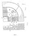
- An integrated circuit assembly l0 includes an integrated circuit die l2 and a multilayer circuit package l4, as shown in FIGS. l, 2 and 3.
- Die l2 is a very large scale integrated (VLSI) circuit.
- Package l4 provides protection and electrical interfacing for the die l2, which is situated in a cavity l6 of the package l4.
- a single bonding shelf l8 of package l4 includes an inner row 20 and an outer row 22 of bonding pads.
- the minimum practical width of the pads is greater than the spacing between pads.
- conductive vias 24 provide for electrical connection of bonding pads 26 of inner row 20 to permit routing below bonding pads 28 of outer row 22.
- bonding pad rows 20 and 22 are staggered to allow maximal and uniform spacing of the bonding wires 30 and 32.
- Bonding wires 30 extend from every other die bonding pad 34 to the opposing package bonding pads 26 of inner row 20.
- Bonding wires 32 extend from the alternate die bonding pads 34 to the respective package bonding pads 28 of outer row 22.
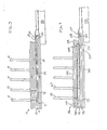
- package l4 is constituted of several layers, including layers 43 and 44, of insulating ceramic material.
- Package l4 also includes a large number of conductive pins, including pins 6l-65, which provide for physical attachment and electrical interfacing to an incorporating system.
- Metallized strips or "fingers" include bonding pads 26 and 28 of FIG. l and serve as conductive paths to the pins.
- the finger to pin 6l includes an inner bonding pad 26, a via 24, a conductive segment 36 along layer 43, and a via 7l.
- the finger to pin 62 includes an outer bonding pad 28, a conductive segment 38 along layer 44, and a via 72. Fingers (not illustrated) to the other pins follow this alternating pattern.
- Integrated circuit assembly ll0 illustrated in Fig. 4, is virtually identical to the embodiment described above except with respect to the conductive paths between the package bonding pads and the pins.
- the conductive finger to pin l62 includes an inner bonding pad l26, via l24, conductive segment 36l along layer l43, via 362 between layers l43 and l44, conductive segment 363 along layer l44 and via l72.
- the conductive finger to pin l6l includes an outer bonding pad l28, conductive segment 38l along layer l44, via 382 between layer l44 and l46, conductive segment 383 along layer l46, and via l7l.
- the metallization patterns of assembly ll0 reflect the dedication of layer l43 as a ground plane so that only an inner portion is practically available for use by input or output signal fingers.
- Layers l43, l45 and l47 are ground planes which can be used to shield the signals carried by layers l44 and l46. Thus, each signal carrying layer l44, l46 is shielded above and below by a shielding layer.
- FIGS. 3 and 4 For purposes of completeness, the embodiments illustrated in FIGS. 3 and 4 are shown with heat spreaders 80 and l80, while FIGS. l and 2 illustrated an embodiment without such a heat spreader, but with the die attached to a ceramic layer of the package. This is done for heat dissipation purposes and forms no part of the present invention.
- the illustrated embodiment includes 260 pins arranged on a 0.l00 ⁇ pitch in a l9 ⁇ l9 array with an opening in the center for the die and a hermetic seal.
- the external package size is about l.96 ⁇ square.
- the ten ceramic layers constitute a total thickness of about 0.l ⁇ .
- the cavity is about 0.5l ⁇ square to accommodate the die which is about 0.4l ⁇ square.
Abstract
Description
- The present invention relates to integrated circuit packaging, and, more particularly, to an integrated circuit package with a novel wire-bond finger layout.
- Most very large scale integrated (VLSI) circuits are fabricated on small silicon or other crystalline substrates. Sophisticated packaging is required to provide electrical interfacing with and protection for these devices. The demands on the integrated circuit package are increased as the required number of input/output and power connections reaches into the hundreds.
- The multilayer ceramic pin-grid array (PGA) is recognized as a most suitable technology for ultradense pin layouts. Conductive paths are formed by screen printing metallization patterns on unfired alumina tape or "green sheets". Interlayer connections are made through via holes which are punched out and filled with a paste of conductive material such as aluminum or tungsten. The green sheets are laminated and co-fired to form a monolithic package with complete electrical paths or "fingers" between pin locations and bonding pads located on a ceramic bonding shelf.
- A package so constructed generally includes a central cavity in which an integrated circuit silicon die can be attached using a gold-silicon eutectic, other hard or soft solder, a silver glass paste or other bonding material. The die is electrically interfaced to the package using bonding wires which extend between bonding pads on the die to respective bonding pads on the bonding shelf. Typically, it is convenient to arrange both the die bonding pads and the package bonding pads in square rows so that the bonding wires can be positioned straight across the gap between the die and the shelf.
- To a point, an increased pin count can be accommodated by decreasing the pitch of the package bonding pads. However, every production technology imposes some minimum practical pitch. For example, a production technology may not permit bonding pads smaller than 5 mils square. Smaller pads may exceed the precision of available automated wire bonding equipment, or impair the reliability of the conductive nature of the bonding pad itself.
- Partial solutions to this problem include radially spreading or fanning the wire bonds so that the bonding pads of the package are on a greater pitch than the bonding pads on the die. This can yield an about 20% practical improvement in pin count. Further increases involve using longer bonding wires that is practical or desirable. Also, the fan arrangement requires each wire to be bonded at a different angle.
- Another approach uses multiple rows of package bonding pads, each on a separate bonding shelf located on a separate tier level. Each tier level is defined by an area of ceramic layer protruding beyond an adjacent layer. By stair-stepping the ceramic layers multiple bonding shelves can be formed. For example, two bonding shelves can each be used to define a square row of package bonding pads at the minimum practical pitch, thus, doubling the pin count that can be accommodated with a single bonding shelf. Typically, the rows are staggered to optimize the spacing of the wires from adjacent die bonding pads.
- The two bonding shelf approach has disadvantages. One problem is in the coregistration of the multiple rows of bonding pads. If the staggering is inexact, the likelihood of the bare bonding wires contacting and shorting is greatly increased. There are several contributors to such misalignment.
- The major source of misalignment is uneven shrinkage during the co-firing of the ceramic package, which can involve heat exposure at l500°C for about 48 hours. Shrinkage can amount to l7%-23% of the area of any given layer, and adjacent layers can shrink in different directions. Furthermore, any problem with shrinkage misalignment is exacerbated when intermediate layers are involved. In addition to misalignment due to shrinkage, the screen printing process introduces alignment errors at each layer.
- What is needed, then, is a practical and economical approach to increasing the pin count that can be accommodated by a packaging scheme without the problems due to layer misalignment.
- In accordance with the present invention, a package for an integrated circuit includes plural rows of bonding pads on a single bonding shelf defined on a single package layer. These rows include an inner and an outer row, defined by their relative proximity to a central cavity where an integrated circuit die is to be positioned. Conductive vias extend from pads of the inner row to a second layer of the package. This permits fingers to the inner row of pads to traverse the package without interference with the fingers to the outer row of pads.
- In a preferred embodiment of the present invention, the via connects with a conductive segment formed on the second layer. This first segment extends to a second via which directly contacts the respective pin. The outer pads are connected to respective pin vias by conductive segments formed on the bonding-shelf layer of the package.
- In another embodiment, design restrictions require a more complex finger routing. Fingers extend from the inner pads down first vias to first conductive segments on a second layer, up second vias to second segments on the bonding-shelf layer, and from there to third vias which connect to the respective pins. Fingers from the outer pads extend along short segments on the bonding-shelf layer, along vias to a third layer, and along conductive segments on this third layer to the vias to the pins. Many other arrangements are made possible by the present invention.
- The present invention provides the advantages of the multiple bonding shelf approach in that multiple staggered rows permit the effective pitch of the bonding pads to be multiplied by a factor of two or more. However, since all bonding pads are on a single bonding shelf, the problems with misalignment are essentially eliminated. This makes for an economical ultra-high density package with improved reliability.
-
- FIGURE l is a planar view of an integrated circuit assembly in accordance with the present invention.
- FIGURE 2 is a sectional view taken along line 2-2 of FIG. l.
- FIGURE 3 is a sectional view of a portion of an integrated circuit assembly in accordance with the present invention.
- FIGURE 4 is a sectional view of a portion of another integrated circuit assembly in accordance with the present invention.
- An integrated circuit assembly l0 includes an integrated circuit die l2 and a multilayer circuit package l4, as shown in FIGS. l, 2 and 3. Die l2 is a very large scale integrated (VLSI) circuit. Package l4 provides protection and electrical interfacing for the die l2, which is situated in a cavity l6 of the package l4.
- To provide a very large number of interconnections between die l2 and package l4, a single bonding shelf l8 of package l4 includes an
inner row 20 and anouter row 22 of bonding pads. The minimum practical width of the pads is greater than the spacing between pads. Thus, in accordance with the present invention,conductive vias 24 provide for electrical connection ofbonding pads 26 ofinner row 20 to permit routing below bondingpads 28 ofouter row 22. - Preferably,
bonding pad rows bonding wires Bonding wires 30 extend from every otherdie bonding pad 34 to the opposingpackage bonding pads 26 ofinner row 20.Bonding wires 32 extend from the alternatedie bonding pads 34 to the respectivepackage bonding pads 28 ofouter row 22. - As shown in FIG. 3, package l4 is constituted of several layers, including
layers bonding pads - The finger to pin 6l includes an
inner bonding pad 26, a via 24, aconductive segment 36 alonglayer 43, and a via 7l. The finger to pin 62 includes anouter bonding pad 28, aconductive segment 38 alonglayer 44, and a via 72. Fingers (not illustrated) to the other pins follow this alternating pattern. - Various design constraints can render an alternative embodiment more optimal. Integrated circuit assembly ll0, illustrated in Fig. 4, is virtually identical to the embodiment described above except with respect to the conductive paths between the package bonding pads and the pins.
- In assembly ll0, the conductive finger to pin l62 includes an inner bonding pad l26, via l24, conductive segment 36l along layer l43, via 362 between layers l43 and l44,
conductive segment 363 along layer l44 and via l72. The conductive finger to pin l6l includes an outer bonding pad l28, conductive segment 38l along layer l44, via 382 between layer l44 and l46,conductive segment 383 along layer l46, and via l7l. - The metallization patterns of assembly ll0 reflect the dedication of layer l43 as a ground plane so that only an inner portion is practically available for use by input or output signal fingers. Layers l43, l45 and l47 are ground planes which can be used to shield the signals carried by layers l44 and l46. Thus, each signal carrying layer l44, l46 is shielded above and below by a shielding layer.
- For purposes of completeness, the embodiments illustrated in FIGS. 3 and 4 are shown with
heat spreaders 80 and l80, while FIGS. l and 2 illustrated an embodiment without such a heat spreader, but with the die attached to a ceramic layer of the package. This is done for heat dissipation purposes and forms no part of the present invention. - The illustrated embodiment includes 260 pins arranged on a 0.l00ʺ pitch in a l9 × l9 array with an opening in the center for the die and a hermetic seal. The external package size is about l.96ʺ square. The ten ceramic layers constitute a total thickness of about 0.lʺ. The cavity is about 0.5lʺ square to accommodate the die which is about 0.4lʺ square. These dimensions are specific to the described embodiment, the invention being applicable to wide variations in such dimensions.
- As is apparent to those skilled in the art, many variations and modifications of the embodiments described above are provided by the present invention. Therefore, the scope of the present invention is limited only by the following claims.
Claims (7)
plural layers, said package defining a cavity, a first of said layers defining a bonding shelf adjacent said cavity;
bonding pads arranged on said bonding shelf in plural rows including an outer row spaced from said cavity and an inner row located between said outer row and said cavity;
electrical contacts physically connected with said package, said contacts providing for electrical communication with an incorporating system; and
conductive paths, each path providing an electrical connection between at least one of said contacts and at least one of said bonding pads, said conductive paths including a first conductive path electrically connecting a first of said bonding pads of said inner row with a first of said contacts, said first conductive path including a conductive first segment disposed upon a second of said layers, said first conductive path including a via electrically connecting said first bonding pad with said first segment so that said first conductive path is electrically isolated from all conductive paths of said outer row.
plural layers, said package defining a cavity, a first of said layers defining a bonding shelf adjacent said cavity;
an integrated circuit disposed within said cavity, said integrated circuit including conductive pads;
bonding pads arranged on said bonding shelf in plural rows including an outer row spaced from said cavity and a inner row located between said outer row and said cavity;
bonding wires for electrically connecting said bonding pads with said conductive pads;
contacts physically connected with said package, said contacts providing for electrical communication with an incorporating system; and
conductive paths, each path defining an electrical connection between at least one of said contacts and at least one of said bonding pads, said conductive paths including a first conductive path electrically connecting a first of said bonding pads of said inner row with a first of said contacts, said first conductive path including a conductive first segment disposed upon a second of said layers.
Applications Claiming Priority (2)
| Application Number | Priority Date | Filing Date | Title |
|---|---|---|---|
| US07/848,302 US4890153A (en) | 1986-04-04 | 1986-04-04 | Single bonding shelf, multi-row wire-bond finger layout for integrated circuit package |
| US848302 | 1992-03-09 |
Publications (2)
| Publication Number | Publication Date |
|---|---|
| EP0240433A2 true EP0240433A2 (en) | 1987-10-07 |
| EP0240433A3 EP0240433A3 (en) | 1988-01-27 |
Family
ID=25302924
Family Applications (1)
| Application Number | Title | Priority Date | Filing Date |
|---|---|---|---|
| EP87400729A Withdrawn EP0240433A3 (en) | 1986-04-04 | 1987-04-03 | Single bonding shelf, multi-row, wire-bond finger layout for integrated circuit package |
Country Status (3)
| Country | Link |
|---|---|
| US (1) | US4890153A (en) |
| EP (1) | EP0240433A3 (en) |
| JP (1) | JPS63260042A (en) |
Cited By (3)
| Publication number | Priority date | Publication date | Assignee | Title |
|---|---|---|---|---|
| EP0750204B1 (en) * | 1995-06-22 | 2005-08-24 | Hitachi, Ltd. | Optical semiconductor array module, method of fabricating the module, and external board mounting structure of the module |
| US7691680B2 (en) | 2003-03-04 | 2010-04-06 | Micron Technologies, Inc. | Method of fabricating microelectronic component assemblies employing lead frames having reduced-thickness inner lengths |
| US7696003B2 (en) | 2004-07-23 | 2010-04-13 | Micron Technology, Inc. | Microelectronic component assemblies with recessed wire bonds and methods of making same |
Families Citing this family (37)
| Publication number | Priority date | Publication date | Assignee | Title |
|---|---|---|---|---|
| GB8918482D0 (en) * | 1989-08-14 | 1989-09-20 | Inmos Ltd | Packaging semiconductor chips |
| EP0463758A1 (en) * | 1990-06-22 | 1992-01-02 | Digital Equipment Corporation | Hollow chip package and method of manufacture |
| US5043794A (en) * | 1990-09-24 | 1991-08-27 | At&T Bell Laboratories | Integrated circuit package and compact assemblies thereof |
| US5155578A (en) * | 1991-04-26 | 1992-10-13 | Texas Instruments Incorporated | Bond wire configuration and injection mold for minimum wire sweep in plastic IC packages |
| US5227583A (en) * | 1991-08-20 | 1993-07-13 | Microelectronic Packaging America | Ceramic package and method for making same |
| US5229917A (en) * | 1992-07-24 | 1993-07-20 | The United States Of America As Represented By The Secretary Of The Air Force | VLSI integration into a 3-D WSI dual composite module |
| WO1994025979A1 (en) * | 1993-04-30 | 1994-11-10 | Lsi Logic Corporation | Integrated circuit with lead frame package having internal power and ground busses |
| US5478420A (en) * | 1994-07-28 | 1995-12-26 | International Business Machines Corporation | Process for forming open-centered multilayer ceramic substrates |
| US7196313B2 (en) * | 2004-04-02 | 2007-03-27 | Fairchild Semiconductor Corporation | Surface mount multi-channel optocoupler |
| US7772681B2 (en) * | 2005-06-30 | 2010-08-10 | Fairchild Semiconductor Corporation | Semiconductor die package and method for making the same |
| US20090057852A1 (en) * | 2007-08-27 | 2009-03-05 | Madrid Ruben P | Thermally enhanced thin semiconductor package |
| US20070164428A1 (en) * | 2006-01-18 | 2007-07-19 | Alan Elbanhawy | High power module with open frame package |
| US7868432B2 (en) * | 2006-02-13 | 2011-01-11 | Fairchild Semiconductor Corporation | Multi-chip module for battery power control |
| US7768075B2 (en) | 2006-04-06 | 2010-08-03 | Fairchild Semiconductor Corporation | Semiconductor die packages using thin dies and metal substrates |
| US7656024B2 (en) | 2006-06-30 | 2010-02-02 | Fairchild Semiconductor Corporation | Chip module for complete power train |
| US7564124B2 (en) * | 2006-08-29 | 2009-07-21 | Fairchild Semiconductor Corporation | Semiconductor die package including stacked dice and heat sink structures |
| US8106501B2 (en) | 2008-12-12 | 2012-01-31 | Fairchild Semiconductor Corporation | Semiconductor die package including low stress configuration |
| US7821116B2 (en) * | 2007-02-05 | 2010-10-26 | Fairchild Semiconductor Corporation | Semiconductor die package including leadframe with die attach pad with folded edge |
| US7659531B2 (en) * | 2007-04-13 | 2010-02-09 | Fairchild Semiconductor Corporation | Optical coupler package |
| US7683463B2 (en) * | 2007-04-19 | 2010-03-23 | Fairchild Semiconductor Corporation | Etched leadframe structure including recesses |
| US7902657B2 (en) * | 2007-08-28 | 2011-03-08 | Fairchild Semiconductor Corporation | Self locking and aligning clip structure for semiconductor die package |
| US20090057855A1 (en) * | 2007-08-30 | 2009-03-05 | Maria Clemens Quinones | Semiconductor die package including stand off structures |
| US7589338B2 (en) * | 2007-11-30 | 2009-09-15 | Fairchild Semiconductor Corporation | Semiconductor die packages suitable for optoelectronic applications having clip attach structures for angled mounting of dice |
| US20090140266A1 (en) * | 2007-11-30 | 2009-06-04 | Yong Liu | Package including oriented devices |
| KR20090062612A (en) * | 2007-12-13 | 2009-06-17 | 페어차일드코리아반도체 주식회사 | Multi chip package |
| US7781872B2 (en) * | 2007-12-19 | 2010-08-24 | Fairchild Semiconductor Corporation | Package with multiple dies |
| US8106406B2 (en) | 2008-01-09 | 2012-01-31 | Fairchild Semiconductor Corporation | Die package including substrate with molded device |
| US7626249B2 (en) * | 2008-01-10 | 2009-12-01 | Fairchild Semiconductor Corporation | Flex clip connector for semiconductor device |
| US20090194856A1 (en) * | 2008-02-06 | 2009-08-06 | Gomez Jocel P | Molded package assembly |
| KR101524545B1 (en) * | 2008-02-28 | 2015-06-01 | 페어차일드코리아반도체 주식회사 | Power device package and the method of fabricating the same |
| US8018054B2 (en) * | 2008-03-12 | 2011-09-13 | Fairchild Semiconductor Corporation | Semiconductor die package including multiple semiconductor dice |
| US7768108B2 (en) | 2008-03-12 | 2010-08-03 | Fairchild Semiconductor Corporation | Semiconductor die package including embedded flip chip |
| KR101519062B1 (en) * | 2008-03-31 | 2015-05-11 | 페어차일드코리아반도체 주식회사 | Semiconductor Device Package |
| US20090278241A1 (en) * | 2008-05-08 | 2009-11-12 | Yong Liu | Semiconductor die package including die stacked on premolded substrate including die |
| US8193618B2 (en) | 2008-12-12 | 2012-06-05 | Fairchild Semiconductor Corporation | Semiconductor die package with clip interconnection |
| US7973393B2 (en) | 2009-02-04 | 2011-07-05 | Fairchild Semiconductor Corporation | Stacked micro optocouplers and methods of making the same |
| US8421204B2 (en) | 2011-05-18 | 2013-04-16 | Fairchild Semiconductor Corporation | Embedded semiconductor power modules and packages |
Citations (3)
| Publication number | Priority date | Publication date | Assignee | Title |
|---|---|---|---|---|
| EP0027017A1 (en) * | 1979-10-04 | 1981-04-15 | Fujitsu Limited | Integrated circuit package |
| GB2077036A (en) * | 1980-05-15 | 1981-12-09 | Cts Corp | Multi-layer ceramic package for semiconductor chip |
| US4513355A (en) * | 1983-06-15 | 1985-04-23 | Motorola, Inc. | Metallization and bonding means and method for VLSI packages |
-
1986
- 1986-04-04 US US07/848,302 patent/US4890153A/en not_active Expired - Lifetime
-
1987
- 1987-04-03 EP EP87400729A patent/EP0240433A3/en not_active Withdrawn
- 1987-04-03 JP JP62081301A patent/JPS63260042A/en active Granted
Patent Citations (3)
| Publication number | Priority date | Publication date | Assignee | Title |
|---|---|---|---|---|
| EP0027017A1 (en) * | 1979-10-04 | 1981-04-15 | Fujitsu Limited | Integrated circuit package |
| GB2077036A (en) * | 1980-05-15 | 1981-12-09 | Cts Corp | Multi-layer ceramic package for semiconductor chip |
| US4513355A (en) * | 1983-06-15 | 1985-04-23 | Motorola, Inc. | Metallization and bonding means and method for VLSI packages |
Non-Patent Citations (1)
| Title |
|---|
| PATENT ABSTRACTS OF JAPAN, vol. 8, no. 95 (E-242)[1532], 2nd May 1984; & JP-A-59 014 652 (NIPPON DENKI K.K.) 25-01-1984 * |
Cited By (3)
| Publication number | Priority date | Publication date | Assignee | Title |
|---|---|---|---|---|
| EP0750204B1 (en) * | 1995-06-22 | 2005-08-24 | Hitachi, Ltd. | Optical semiconductor array module, method of fabricating the module, and external board mounting structure of the module |
| US7691680B2 (en) | 2003-03-04 | 2010-04-06 | Micron Technologies, Inc. | Method of fabricating microelectronic component assemblies employing lead frames having reduced-thickness inner lengths |
| US7696003B2 (en) | 2004-07-23 | 2010-04-13 | Micron Technology, Inc. | Microelectronic component assemblies with recessed wire bonds and methods of making same |
Also Published As
| Publication number | Publication date |
|---|---|
| US4890153A (en) | 1989-12-26 |
| JPS63260042A (en) | 1988-10-27 |
| EP0240433A3 (en) | 1988-01-27 |
| JPH03779B2 (en) | 1991-01-08 |
Similar Documents
| Publication | Publication Date | Title |
|---|---|---|
| US4890153A (en) | Single bonding shelf, multi-row wire-bond finger layout for integrated circuit package | |
| US7129574B2 (en) | Multi-power ring chip scale package for system level integration | |
| JP4592122B2 (en) | Flip chip package with reduced number of package layers | |
| US8129837B2 (en) | Flip chip interconnection pad layout | |
| US5373188A (en) | Packaged semiconductor device including multiple semiconductor chips and cross-over lead | |
| US5467252A (en) | Method for plating using nested plating buses and semiconductor device having the same | |
| US5717245A (en) | Ball grid array arrangement | |
| US5858815A (en) | Semiconductor package and method for fabricating the same | |
| US6888240B2 (en) | High performance, low cost microelectronic circuit package with interposer | |
| US5982632A (en) | Short power signal path integrated circuit package | |
| EP0807369A1 (en) | Stackable modules and multimodular assemblies | |
| JPH0587977B2 (en) | ||
| EP0729645B1 (en) | A high density integrated circuit assembly combining leadframe leads with conductive traces | |
| US5650660A (en) | Circuit pattern for a ball grid array integrated circuit package | |
| US5569955A (en) | High density integrated circuit assembly combining leadframe leads with conductive traces | |
| JP2001351983A (en) | Semiconductor device and its manufacturing method | |
| US5726860A (en) | Method and apparatus to reduce cavity size and the bondwire length in three tier PGA packages by interdigitating the VCC/VSS | |
| EP1361612A2 (en) | Organic substrate for flip chip bonding | |
| JPS5854661A (en) | Multilayer ceramic semiconductor package | |
| EP0272188A2 (en) | Ceramic package for high frequency semiconductor devices | |
| US11688678B2 (en) | Wiring board and semiconductor device | |
| EP0398628A2 (en) | Semiconductor memory device | |
| EP0262493B1 (en) | Electronic package with distributed decoupling capacitors | |
| US7105926B2 (en) | Routing scheme for differential pairs in flip chip substrates | |
| JPH0645386A (en) | Semiconductor circuit device |
Legal Events
| Date | Code | Title | Description |
|---|---|---|---|
| PUAI | Public reference made under article 153(3) epc to a published international application that has entered the european phase |
Free format text: ORIGINAL CODE: 0009012 |
|
| AK | Designated contracting states |
Kind code of ref document: A2 Designated state(s): DE FR GB IT NL |
|
| PUAL | Search report despatched |
Free format text: ORIGINAL CODE: 0009013 |
|
| AK | Designated contracting states |
Kind code of ref document: A3 Designated state(s): DE FR GB IT NL |
|
| 17P | Request for examination filed |
Effective date: 19880823 |
|
| 17Q | First examination report despatched |
Effective date: 19900810 |
|
| STAA | Information on the status of an ep patent application or granted ep patent |
Free format text: STATUS: THE APPLICATION IS DEEMED TO BE WITHDRAWN |
|
| 18D | Application deemed to be withdrawn |
Effective date: 19920501 |
|
| RIN1 | Information on inventor provided before grant (corrected) |
Inventor name: WU, CHING-AN |