EP0241316A2 - Method for forming crystalline deposited film - Google Patents
Method for forming crystalline deposited film Download PDFInfo
- Publication number
- EP0241316A2 EP0241316A2 EP87303224A EP87303224A EP0241316A2 EP 0241316 A2 EP0241316 A2 EP 0241316A2 EP 87303224 A EP87303224 A EP 87303224A EP 87303224 A EP87303224 A EP 87303224A EP 0241316 A2 EP0241316 A2 EP 0241316A2
- Authority
- EP
- European Patent Office
- Prior art keywords
- nucleation
- ndl
- forming
- substrate
- nds
- Prior art date
- Legal status (The legal status is an assumption and is not a legal conclusion. Google has not performed a legal analysis and makes no representation as to the accuracy of the status listed.)
- Granted
Links
Images


Classifications
-
- H—ELECTRICITY
- H01—ELECTRIC ELEMENTS
- H01L—SEMICONDUCTOR DEVICES NOT COVERED BY CLASS H10
- H01L21/00—Processes or apparatus adapted for the manufacture or treatment of semiconductor or solid state devices or of parts thereof
- H01L21/02—Manufacture or treatment of semiconductor devices or of parts thereof
- H01L21/02104—Forming layers
- H01L21/02365—Forming inorganic semiconducting materials on a substrate
- H01L21/02367—Substrates
- H01L21/0237—Materials
- H01L21/02422—Non-crystalline insulating materials, e.g. glass, polymers
-
- C—CHEMISTRY; METALLURGY
- C23—COATING METALLIC MATERIAL; COATING MATERIAL WITH METALLIC MATERIAL; CHEMICAL SURFACE TREATMENT; DIFFUSION TREATMENT OF METALLIC MATERIAL; COATING BY VACUUM EVAPORATION, BY SPUTTERING, BY ION IMPLANTATION OR BY CHEMICAL VAPOUR DEPOSITION, IN GENERAL; INHIBITING CORROSION OF METALLIC MATERIAL OR INCRUSTATION IN GENERAL
- C23C—COATING METALLIC MATERIAL; COATING MATERIAL WITH METALLIC MATERIAL; SURFACE TREATMENT OF METALLIC MATERIAL BY DIFFUSION INTO THE SURFACE, BY CHEMICAL CONVERSION OR SUBSTITUTION; COATING BY VACUUM EVAPORATION, BY SPUTTERING, BY ION IMPLANTATION OR BY CHEMICAL VAPOUR DEPOSITION, IN GENERAL
- C23C16/00—Chemical coating by decomposition of gaseous compounds, without leaving reaction products of surface material in the coating, i.e. chemical vapour deposition [CVD] processes
- C23C16/04—Coating on selected surface areas, e.g. using masks
-
- C—CHEMISTRY; METALLURGY
- C23—COATING METALLIC MATERIAL; COATING MATERIAL WITH METALLIC MATERIAL; CHEMICAL SURFACE TREATMENT; DIFFUSION TREATMENT OF METALLIC MATERIAL; COATING BY VACUUM EVAPORATION, BY SPUTTERING, BY ION IMPLANTATION OR BY CHEMICAL VAPOUR DEPOSITION, IN GENERAL; INHIBITING CORROSION OF METALLIC MATERIAL OR INCRUSTATION IN GENERAL
- C23C—COATING METALLIC MATERIAL; COATING MATERIAL WITH METALLIC MATERIAL; SURFACE TREATMENT OF METALLIC MATERIAL BY DIFFUSION INTO THE SURFACE, BY CHEMICAL CONVERSION OR SUBSTITUTION; COATING BY VACUUM EVAPORATION, BY SPUTTERING, BY ION IMPLANTATION OR BY CHEMICAL VAPOUR DEPOSITION, IN GENERAL
- C23C16/00—Chemical coating by decomposition of gaseous compounds, without leaving reaction products of surface material in the coating, i.e. chemical vapour deposition [CVD] processes
- C23C16/22—Chemical coating by decomposition of gaseous compounds, without leaving reaction products of surface material in the coating, i.e. chemical vapour deposition [CVD] processes characterised by the deposition of inorganic material, other than metallic material
- C23C16/24—Deposition of silicon only
-
- C—CHEMISTRY; METALLURGY
- C23—COATING METALLIC MATERIAL; COATING MATERIAL WITH METALLIC MATERIAL; CHEMICAL SURFACE TREATMENT; DIFFUSION TREATMENT OF METALLIC MATERIAL; COATING BY VACUUM EVAPORATION, BY SPUTTERING, BY ION IMPLANTATION OR BY CHEMICAL VAPOUR DEPOSITION, IN GENERAL; INHIBITING CORROSION OF METALLIC MATERIAL OR INCRUSTATION IN GENERAL
- C23C—COATING METALLIC MATERIAL; COATING MATERIAL WITH METALLIC MATERIAL; SURFACE TREATMENT OF METALLIC MATERIAL BY DIFFUSION INTO THE SURFACE, BY CHEMICAL CONVERSION OR SUBSTITUTION; COATING BY VACUUM EVAPORATION, BY SPUTTERING, BY ION IMPLANTATION OR BY CHEMICAL VAPOUR DEPOSITION, IN GENERAL
- C23C16/00—Chemical coating by decomposition of gaseous compounds, without leaving reaction products of surface material in the coating, i.e. chemical vapour deposition [CVD] processes
- C23C16/44—Chemical coating by decomposition of gaseous compounds, without leaving reaction products of surface material in the coating, i.e. chemical vapour deposition [CVD] processes characterised by the method of coating
-
- C—CHEMISTRY; METALLURGY
- C30—CRYSTAL GROWTH
- C30B—SINGLE-CRYSTAL GROWTH; UNIDIRECTIONAL SOLIDIFICATION OF EUTECTIC MATERIAL OR UNIDIRECTIONAL DEMIXING OF EUTECTOID MATERIAL; REFINING BY ZONE-MELTING OF MATERIAL; PRODUCTION OF A HOMOGENEOUS POLYCRYSTALLINE MATERIAL WITH DEFINED STRUCTURE; SINGLE CRYSTALS OR HOMOGENEOUS POLYCRYSTALLINE MATERIAL WITH DEFINED STRUCTURE; AFTER-TREATMENT OF SINGLE CRYSTALS OR A HOMOGENEOUS POLYCRYSTALLINE MATERIAL WITH DEFINED STRUCTURE; APPARATUS THEREFOR
- C30B25/00—Single-crystal growth by chemical reaction of reactive gases, e.g. chemical vapour-deposition growth
- C30B25/02—Epitaxial-layer growth
- C30B25/18—Epitaxial-layer growth characterised by the substrate
-
- H—ELECTRICITY
- H01—ELECTRIC ELEMENTS
- H01L—SEMICONDUCTOR DEVICES NOT COVERED BY CLASS H10
- H01L21/00—Processes or apparatus adapted for the manufacture or treatment of semiconductor or solid state devices or of parts thereof
- H01L21/02—Manufacture or treatment of semiconductor devices or of parts thereof
- H01L21/02104—Forming layers
- H01L21/02365—Forming inorganic semiconducting materials on a substrate
- H01L21/02367—Substrates
- H01L21/0237—Materials
- H01L21/02373—Group 14 semiconducting materials
- H01L21/02381—Silicon, silicon germanium, germanium
-
- H—ELECTRICITY
- H01—ELECTRIC ELEMENTS
- H01L—SEMICONDUCTOR DEVICES NOT COVERED BY CLASS H10
- H01L21/00—Processes or apparatus adapted for the manufacture or treatment of semiconductor or solid state devices or of parts thereof
- H01L21/02—Manufacture or treatment of semiconductor devices or of parts thereof
- H01L21/02104—Forming layers
- H01L21/02365—Forming inorganic semiconducting materials on a substrate
- H01L21/02436—Intermediate layers between substrates and deposited layers
- H01L21/02439—Materials
- H01L21/02488—Insulating materials
-
- H—ELECTRICITY
- H01—ELECTRIC ELEMENTS
- H01L—SEMICONDUCTOR DEVICES NOT COVERED BY CLASS H10
- H01L21/00—Processes or apparatus adapted for the manufacture or treatment of semiconductor or solid state devices or of parts thereof
- H01L21/02—Manufacture or treatment of semiconductor devices or of parts thereof
- H01L21/02104—Forming layers
- H01L21/02365—Forming inorganic semiconducting materials on a substrate
- H01L21/02518—Deposited layers
- H01L21/02521—Materials
- H01L21/02524—Group 14 semiconducting materials
- H01L21/02532—Silicon, silicon germanium, germanium
-
- H—ELECTRICITY
- H01—ELECTRIC ELEMENTS
- H01L—SEMICONDUCTOR DEVICES NOT COVERED BY CLASS H10
- H01L21/00—Processes or apparatus adapted for the manufacture or treatment of semiconductor or solid state devices or of parts thereof
- H01L21/02—Manufacture or treatment of semiconductor devices or of parts thereof
- H01L21/02104—Forming layers
- H01L21/02365—Forming inorganic semiconducting materials on a substrate
- H01L21/02612—Formation types
- H01L21/02617—Deposition types
- H01L21/0262—Reduction or decomposition of gaseous compounds, e.g. CVD
-
- H—ELECTRICITY
- H01—ELECTRIC ELEMENTS
- H01L—SEMICONDUCTOR DEVICES NOT COVERED BY CLASS H10
- H01L21/00—Processes or apparatus adapted for the manufacture or treatment of semiconductor or solid state devices or of parts thereof
- H01L21/02—Manufacture or treatment of semiconductor devices or of parts thereof
- H01L21/02104—Forming layers
- H01L21/02365—Forming inorganic semiconducting materials on a substrate
- H01L21/02612—Formation types
- H01L21/02617—Deposition types
- H01L21/02636—Selective deposition, e.g. simultaneous growth of mono- and non-monocrystalline semiconductor materials
- H01L21/02639—Preparation of substrate for selective deposition
-
- H—ELECTRICITY
- H01—ELECTRIC ELEMENTS
- H01L—SEMICONDUCTOR DEVICES NOT COVERED BY CLASS H10
- H01L21/00—Processes or apparatus adapted for the manufacture or treatment of semiconductor or solid state devices or of parts thereof
- H01L21/02—Manufacture or treatment of semiconductor devices or of parts thereof
- H01L21/02104—Forming layers
- H01L21/02365—Forming inorganic semiconducting materials on a substrate
- H01L21/02612—Formation types
- H01L21/02617—Deposition types
- H01L21/02636—Selective deposition, e.g. simultaneous growth of mono- and non-monocrystalline semiconductor materials
- H01L21/02647—Lateral overgrowth
Abstract
Description
- This invention relates to a method for forming a crystalline deposited film, particularly to a method for forming a crystalline deposited film of a single crystal or a polycrystal controlled in grain size prepared by utilizing the difference in nucleation density of the deposited materials according to the kinds of the deposited surface materials.
- The present invention is applicable for formation of a crystalline deposited film such as a single crystal or a polycrystal to be used for electronic devices, optical devices, magnetic devices, piezoelectric devices or surface acoustic devices, etc., such as semiconductor integrated circuits, optical integrated circuits, magnetic circuits, etc.
- In the prior art, single crystal thin film to be used for semiconductor electronic devices or optical devices have been formed by epitaxial growth on a single crystal substrate. For example, it has been known that epitaxial growth of Si, Ge, GaAs, etc., can be done from liquid phase, gas phase or solid phase on Si single crystal substrate (silicon wafer), and it has been also known that epitaxial growth of a single crystal such as GaAs, GaAlAs, etc., occurs on a GaAs single crystal substrate. By use of the semiconductor thin film thus formed, semiconductor devices and integrated circuits, electroluminescent devices such as semiconductor lasers or LED have been prepared.
- Also, researches and developments have been recently made abundantly about ultra-high speed transistors by use of two-dimensional electronic gas, ultra-lattice devices utilizing quantum well etc., and what has made these possible is the high precision epitaxial technique such as MBE (molecular beam epitaxy) or MOCVD (organometallic chemical vapor deposition) by use of ultra-high vacuum.
- In such epitaxial growth on a single crystal substrate, it is necessary to take matching in lattice constants and coefficient of thermal expansion between the single crystal material of the substrate and the epitaxial growth layer. For example, although it is possible to effect epitaxial growth of Si single crystal thin film on sapphire which is a insulating single crystal substrate, the crystal lattice defect at the interface due to deviation in lattice constant and diffusion of aluminum which is a component of sapphire to the epitaxial layer pose problems in application for electronic devices or circuits.
- Thus, the method for forming a single crystal thin film of the prior art by epitaxial growth may be understood to be dependent greatly on its substrate material. Mathews et al have examined about combinations of the substrate material with epitaxial growth layer (EPITAXIAL GROWTH, Academic Press, New York, 1975, ed. by J.W. Mathews).
- Also, the size of the substrate is presently about 6 inches for Si wafer, and enlargement of GaAs, sapphire substrate is further retarded. In addition, since the single crystal substrate is high in production cost, the cost per chip becomes higher.
- Thus, for production of a single crystal layer capable of preparing a device of good quality according to the method of prior art, there has been involved the problem the kinds of the substrate materials are limited to an extremely narrow scope.
- On the other hand, researches and developments of three-dimensional integrated circuits to accomplish high integration and multi-function by laminating semiconductor devices in the normal line direction of the substrate have been abundantly made in recent years, and also researches and developments of large area semiconductor devices such as solar batteries or switching transistors of liquid crystal picture elements, etc., in which devices are arranged in an array on a cheap glass are becoming more abundant from year to year.
- What is common to both of these is that the technique for forming a semiconductor thin film on an amorphous insulating material and forming an electronic device such as transistor, etc., thereon is required. Among them, particularly the technique for forming a single crystal semiconductor of high quality on an amorphous insulating material has been desired.
- Generally speaking, when a thin film is deposited on an amorphous insulating material substrate such as SiO₂, etc., due to the defect of long distance order of the substrate material, the crystal structure of the deposited film becomes amorphous or polycrystalline. Here, the amorphous film refers to a state in which near distance order to the extent of the closest atoms is preserved, but no longer distance order exists, while the polycrystalline film refers to single crystal grains having no specific crystal direction gathered as separated at the grain boundaries.
- For example, in the case of forming Si on SiO₂ according to the CVD method, if the deposition temperature is about 600 °C or lower, it becomes an amorphous silicon, while it becomes a polycrystalline silicon with grain sizes distributed between some hundred to some thousand Å at a temperature higher than said temperature. However, the grain sizes and their distribution of polycrystalline silicon will be varied greatly depending on the formation method.
- Further, by melting and solidifying an amorphous or polycrystalline film by an energy beam such as laser or rod-shaped heater, etc., a polycrystalline thin film with great grain sizes of some microns or millimeters have bee obtained (Single Crystal silicon on non-single-crystal insulator, Journal of crystal Growth vol, 63, No. 3, Octover, 1983 edited by G.W. Cullen).
- When a transistor is formed on the thus formed thin film of respective crystal structures and electron mobility is measured from its characteristics, mobility of about 0.1 cm²/V · sec or less is obtained for amorphous silicon, mobility of 1 to 10 cm²/V · sec for polycrystalline silicon having grain sizes of some hundred Å, and a mobility to the same extent as in the case of single crystalline silicon for polycrystalline silicon with great grain sizes by melting and solidification.
- From these results, it can be understood that there is great difference in electrical properties between the device formed in the single crystal region within the crystal grains and the device formed as bridging across the grain boundary. In other words, the deposited film on the amorphous material obtained in the prior art becomes amorphous or polycrystalline structure having grain size distribution, and the device prepared thereon is greatly inferior in its performance as compared with the device prepared on the single crystal layer. For this reason, the uses are limited to simple switching devices, solar batteries, photoelectric converting devices, etc.
- On the other hand, the method for forming a polycrystalline thin film with great grain sizes by melting and solidification had the problems that an enormous time is required due to scanning of amorphous or single crystal thin film with energy beam for every wafer to be poor in bulk productivity, and also that it is not suited for enlargement of area.
- Further, in recent years, studies of diamond thin film growth are becoming popular. Diamond thin film, which is particularly broad in bandgap as 5.5 eV as the semiconductor, can be actuated at higher temperature (about 500 °C or less) as compared with Si, Ge, GaAs, etc., which are semiconductor materials of the prior art. Also, the carrier mobility of both electrons and positive holes surpass that of Si (1800 cm²/V · sec for electrons, 1600 cm²/V · sec for positive holes), and thermal conductivity is also extremely high. For this reason, it has been expected to be promising for application in semiconductor devices of the great consumption power type with great heat generation quantity.
- However, although there have been reports in the prior art about epitaxial growth of diamond thin film on a diamond substrate by vapor phase growth (N. Fujimoto, T. Imai and A. doi Pro. of Int. couf. IPAT), there is no successful report about heteroepitaxial growth on a substrate other than diamond substrate.
- Generally speaking, diamond nuclei are generated by utilizing excitation with microwave, using a hydrocarbon type gas such as CH₄, etc., and by irradiation with hot filament or electron beam, but the nucleation density is generally low, whereby a continuous thin film can be obtained with difficulty. Even if a continuous thin film may be formed, it has a polycrystalline structure with great grain size distribution and can be difficultly applied for semiconductor device.
- Also, as long as a diamond substrate is used, it is expensive as a matter of course, posing also a problem in enlargement of area. Thus, it is not suitable for practical application.
- As described above, in the crystal growth method of the prior art and the crystal formed thereby, three-dimensional integration or enlargement of area could not be done with ease to be difficultly applied practically for devices, and crystals such as single crystals and polycrystals, etc., required for preparation of devices having excellent characteristics could not be formed easily and at low cost.
- On the other hand, hitherto, for formation of functional films, particularly crystalline semiconductor films, suitable film forming methods have been individually employed from the standpoint of desired physical characteristics, uses, etc.
- For example, for formation of silicon deposited films such as of amorphous or polycrystalline, i.e. non-single crystalline, silicon which are optionally compensated for lone pair electrons with a compensating agent such as hydrogen atoms (H) or halogen atoms(X), etc., (hereinafter abbreviated as "NON-Si (H,X)", particularly "A-Si (H,X)" when indicating amorphous silicon and "poly-Si (H,X)" when indicating polycrystalline silicon) (the so-called microcrystalline silicon is included within the category of A-Si (H,X) as a matter of course), there have been employed the vacuum vapor deposition method, the plasma CVD method, the thermal CVD method, the reactive sputtering method, the ion plating method, the optical CVD method, etc. Generally, the plasma CVD method has been widely used and industrialized.
- However, the reaction process in formation of a silicon deposited film according to the plasma CVD method which has been generalized in the prior art is considerably complicated as compared with the conventional CVD method, and its reaction mechanism involves not a few unclarified points. Also, there exist a large number of parameters for formation of a deposited film such as substrate temperature, flow rate and flow rate ratio of gases to be introduced, pressure during formation, high frequency power, electrode structure, structure of a reaction vessel, speed of evacuation, plasma generating system, etc. By use of a combination of such a large number of parameters, plasma may sometimes become unstable state, whereby marked deleterious influences were exerted frequently on a deposited film formed. Besides, parameters characteristic of film forming devices must be selected for each device and therefore under the present situation it has been difficult to generalize the production condition.
- Also, in the case of the plasma CVD method, since plasma is directly generated by high frequency or microwave, etc., in a film forming space in which a substrate on which film is to be formed is placed, electrons or a number of ion species generated thereby may give damages to the film in the film forming process to cause lowering in film quality or non-uniformization of film quality. Moreover, the condition suitable for crystallization of a deposited film is restricted and therefore it has been deemed to be difficult to produce a polycrystalline deposited film with stable characteristics.
- On the other hand, for formation of an epitaxial deposited film such as of silicon, germanium, group II-VI or Group III-V semiconductors, etc., there have been used the gas phase epitaxy and the liquid phase epitaxy as defined in a broad sense (generally speaking, the strict definition of epitaxy is to grow another single crystal on a single crystal, both having the same single crystal axes, but here epitaxy is interpreted in a broader sense and it is not limited to the growth onto a single crystal substrate).
- The liquid phase epitaxy is a method for precipitating a semiconductor crystal on a substrate by dissolving a starting material for semiconductor at high temperature to a super-saturated state in a solvent metal which is molten to a liquid and cooling the solution. According to this method, since crystals are grown under a state most approximate to thermal equilibrium among various epitaxy techniques, crystals with high perfectness can be obtained, but on the other hand, bulk productivity is poor and surface state is bad. For such reason, in an optical device which requires an epitaxial layer which is thin and also uniform in thickness, problems are accompanied such as yield in device production, or influences exerted on device characteristics, etc., and therefore this method is not frequently used.
- On the other hand, the gas phase epitaxy has been attempted by physical methods such as the vacuum vapor deposition method, the sputtering method, etc., or chemical methods such as hydrogen reduction of a metal chloride or otherwise thermal pyrolysis of a metal organic compound or a metal hydride. Among them, the molecular beam epitaxy which is a kind of the vacuum vapor deposition method is a dry process under ultra-high vacuum, and therefore high purification and low temperature growth of crystals are possible, whereby there is the advantage that comoposition and concentration can be well controlled to give a relatively flat deposited film. However, in addition to an enormous cost required for a film forming device, the surface defect density is great, and no effective method for controlling directionality of molecular beam has been developed, and also enlargement of area is difficult and bulk productivity is not so high. Due to such many problems, it has not been industrialized yet.
- The hydrogen reduction method of a metal chloride or the thermal pyrolysis method of a metal organic compound or a metal hydride are generally called the halide CVD method, the hydride CVD method, MO-CVD method. for these methods, by the reason that a film forming device can be made with relative ease and also as the starting materials, i.e. metal chloride, metal hydrides and organic metals, those with high purities are now readily available, they have studied widely at the present time and application for various devices has been investigated.
- However, in these methods, it is required to heat a substrate to a high temperature at which reduction reaction or thermal pyrolysis reaction can occur and therefore the scope of substrate material to be selected is limited, and also contamination with impurities such as carbon or halogen, etc., is liable to cause if decomposition of starting material is insufficient, thus having the drawback that controllability of doping is poor. Also while, depending on the application use of a deposited film, it is desired to effect bulk production with reproducibility with full satisfaction in terms of enlargement of area, uniformization of film thickness as well as uniformness of film quality and yet at a high speed film formation, under the present situation no technique which enables bulk production with maintaining practical characteristics satisfying the above demands has been established yet.
- A main object of the present invention is to provide a method for forming a crystalline deposited film which has overcome the problems of the prior art as described above.
- Another object of the present invention is to provide a method for forming a crystal of good quality such as single crystal containing no grain boundary or a polycrystal controlled in grain boundary, etc., without restriction with respect to the base materials, for. example, without restriction with respect to materials, constitutions, sizes, etc., of the substrate.
- Still another object of the present invention is to provide a method for forming the above crystal with good efficiency according to simple steps without use of a special device.
- Still another object of the present invention is to provide a method for forming a deposited film which is easy in control of film quality simultaneously with saving energy and can give a crystalline deposited film having desired characteristics uniformly over a large area and excellent in semiconductive characteristics.
- A further object of the present invention is to provide a method for forming a deposited film which is excellent in productivity and bulk productivity and can form simply and efficiently a crystalline deposited film having high quality and excellent physical characteristics such as electrical, optical or semiconductive characteristics, etc.
- According to the present invention, there is provided a method for forming a crystalline deposited film, which comprises introducing an active species (A) formed through decomposition of a compound containing silicon and a halogen and an active species (B) formed from a chemical substance for film formation having a property of effecting chemical mutual reaction with said active species (A) into a film forming space in which a substrate having a free surface with a nonnucleation surface (SNDS) with smaller nucleation density and a nucleation surface (SNDL) having sufficiently small area for crystal growth from only a single nucleus and having greater nucleation density (NDL) than the nucleation density (NDS) of said nonnucleation surface (SNDS) being arranged adjacent thereto is previously arranged, thereby forming a single crystal on said nucleation surface (SNDL) and permitting a single crystal to grow from said nucleus.
- The method for forming a deposited film of the present invention having the above constitution has one specific feature in forming a deposited film by use of active species without utilizing plasma reaction while the plasma CVD method of the prior art forms plasma discharging by permitting discharging energy, etc., to act on starting gases for formation of a deposited film, and therefore, the present method is not subjected to any bad influence by etching or abnormal discharging, etc., during film formation will not be raised.
- Also, the method for forming a deposited film of the present invention utilizes the reaction of an active species (A) obtained by decomposing a compound (SX) containing silicon and a halogen which contains constituent elements of a deposited film with an active species (B) formed from a chemical substance and requires no high temperature for deposition, and therefore there is no disturbance of structure by heat, and no heating installation during production and no expense accompanied with running thereof are required, whereby a device can be made lower in cost. And, it becomes possible to select the substrate material from a wide scope of materials without depending on heat resistance.
- Also, the method for forming a deposited film of the present invention forms a deposited film according to the reaction between an active species (A) and an active species (B) and enlargement of area is facilitated not depending on the shape and the size of the substrate, and at the same time starting materials employed may be very small in amounts, whereby the film forming space can be made smaller to improve dramatically the yield.
- Also, according to the method for forming deposited film of the present invention, the size of the crystal grain can be determined by arranging the nucleus for crystal growth as desired on the substrate, whereby a crystalline deposited film having characteristics suited for the purpose can be deposited at any desired region.
- Also, according to the method for forming deposited film of the present invention with the constitution as described above, it becomes possible to form a good crystalline deposited film having uniform film quality and characteristics over a large area with easy control of film quality simultaneously with energy saving in formation of deposited film. Further, a crystalline deposited film of high quality with excellent characteristics such as electrical, optical, semiconductor characteristics can be obtained efficiently with excellent productivity and bulk productivity.
-
- Fig. 1 is a graph for illustration of the relationship between the size of nucleus rc and free energy G in the process of forming thin film;
- Figs. 2(A) and 2(B) are illustrations of the selective deposition method;
- Fig. 3 is a graph showing the change with lapse of time of nucleation density (ND) on the deposition surface of SiO₂ and the deposition surface of silicon nitride;
- Figs. 4(A) to 4(D) are illustra†ions of the formation steps showing a first embodiment of the method for forming crystal according to the present invention;
- Figs. 5(A) and 5(B) are perspective views of the substrate in Figs. 4(A) and 4(D);
- Figs. 6(A) to 6(D) are illustrations of the steps for forming crystal showing a second embodiment of the present invention;
- Figs. 7(A) to 7(D) are illustrations of the formation steps showing a third embodiment of the method for forming single crystal according to the present invention;
- Figs. 8(A) and 8(B) are perspective views of the substrates in Figs. 7(A) and 7(D);
- Figs. 9(A) to 9(D) are illustrations of the steps for forming crystal showing a fourth embodiment of the present invention;
- Figs. 10(A) to 10(C) are illustrations of formation steps showing a fifth embodiment of the method for forming crystal according to the present invention;
- Figs. 11(A) and 11(B) are perspective views of the substrates in Figs. 10(A) and 10(C);
- Figs. 12(A) to 12(C) are illustrations of the formation steps of crystal showing a sixth embodiment of the present invention;
- Figs. 13(A) to 13(C) are illustrations of the formation steps of crystal showing a seventh embodiment of the present invention;
- Fig. 14 is a schematic sectional view showing an example of the multi-layer structure by use of the first embodiment of the present invention;
- Figs. 15(A) to 15(D) are illustrations of the steps for forming crystal showing an eighth embodiment of the present invention;
- Fig. 16 is a graph showing the relationship between the flow rate ratio of SiH₄ and NH₃ and the composition ratio of Si and N in the silicon nitride film formed;
- Fig. 17 is a graph showing the relationship between Si/N composition ratio and nucleation density;
- Fig. 18 is a graph showing the relationship between the injected amount of Si ions and nucleations density;
- Figs. 19(A) to 19(D) are illustrations of the formation steps showing a ninth embodiment of the method for forming crystal according to the present invention;
- Figs. 20(A) and 20(B) are perspective views of the substrate in Figs. 19(A) and 19(D);
- Figs. 21(A) to 21(D) are illustrations of the steps for forming crystal showing a tenth embodiment of the present invention;
- Figs. 22(A) to 22(D) are illustrations of the formation steps showing an eleventh embodiment of the method for forming single crystal according to the present invention;
- Figs. 23(A) and 23(B) are perspective views of the substrates in Figs. 22(A) and 22(D)
- Figs. 24(A) to 24(C) are illustrations of the steps for forming crystal showing a twelfth embodiment of the present invention;
- Figs. 25(A) and 25(B) are pespective views of the substrates in Figs. 24(A) and 24(C);
- Figs. 26(A) to 26(D) are illustrations of the formation steps of crystal showing a thirteenth embodiment of the present invention;
- Fig. 27 is a schematic illustration of the film-forming device used in Examples of the present invention;
- Figs. 28(A) to 28(F) are diagrams of the film forming steps according to the present invention;
- Figs. 29(A) to 29(E) are diagrams of another film forming steps according to the present invention;
- Fig. 30 is a schematic sectional view showing an example of the deposited film obtained on the specific substrate according to the present invention; and
- Fig. 31 is a schematic structural view of a TFT fabricated utilizing the deposition film obtained by the present invention.
- In the present invention, the activated species (A) from the activation space (A) should preferably be selected and used as desired from those having the life of 0.1 sec. or longer, more preferably 1 sec. or longer, optimally 10 sec. or longer, from the standpoint of productivity and easiness in handling, and the constituent elements of the active species (A) become the components constituting the deposited film formed in the film forming space. Also, the chemical substance for film formation is activated to become the active species (B) by the action of an activation energy in the activation space (B) before introduction into the film forming space, and introduced from the activation space (A) at the same time during formation of the deposited film to undergo chemical mutual reaction with the active species (A) containing constituent elements which become the constituent components of the deposited film formed.
- In the present invention, as the compound containing silicon and halogen to be introduced into the activation space (A), there may be employed, for example, chain or cyclic silane compounds of which hydrogen atoms are partially or wholly substituted with halogen atoms, typically chain silicon halides represented by SiuY2u+2(u is an interger of 1 or more, Y is at least one element selected from F, Cl, Br and I) and cyclic silicon halides SivY2v (v is an integer of 3 or more, and Y has the same meaning as defined above), chain and cyclic ompounds represented by SiuHxYy (u and Y have the same meaning as defined above, x + y = 2u or 2u + 2).
- Specific examples may include gaseous or readily gasifiable compounds such as SiF₄, (SiF₂)₅, (SiF₂)₆, (SiF₂)₄, Si₂F₆, Si₃F₈, SiHF₃, SiH₂F₂, SiCl₄, (SiCl₂)₅, SiBr₄, (SiBr₂)₅, Si₂Cl₆, Si₂Br₆, SiHCl₃, SiH₂Cl₂, SiH₃Cl, SiHBr₃, SiHI₃, Si₂Cl₃F₃, and the like.
- For formation of the activated species (A), in addition to the above compound containing silicon and halogen, other silicon compounds, simple substance of silicon, hydrogen, halogen gases (e.g. F₂ gas, CI₂ gas, gasified Br₂, I₂, etc.) can be used in combination, if desired.
- In the present invention, as the method for forming activated species (A) in the activation space (A), there may be employed various activation energies such as electrical energies, including microwave, RF, low frequency DC, etc., heat energies such as heater heating, IR-ray heating, etc., photoenergy, etc. in view of respective conditions and the device.
- As the above chemical substance for film formation for forming active species (B) in the activation space (B), hydrogen gas and/or halogen gases (e.g. F₂ gas, Cl₂ gas, gasified Br₂, I₂, etc.) may be advantageously used. Also, in addition to these chemical substances for film formation, for example, an inert gas such as helium, argon, neon, etc., may be employed. When a plural number of these chemical substances for film formation are employed, they can be previously mixed and introduced under gaseous state into the activation space (B), or alternatively these chemical substances for film formation may be fed individually from the respective independent feeding sources to be introduced into the activation space (B), or they can be introduced into the respective independent activation spaces to be individually activated.
- In the present invention, the proportion in amount of the above activated species (A) to the activated species (B) to be introduced into the film forming space may suitably be determined depending on the depositing conditions, the kind of the activated species, etc., but may preferably be 10 : 1 to 1 : 10, more preferably 8 : 2 to 4 : 6.
- Also, the deposited film formed according to the present invention can be doped with an impurity element so-called in the art of semiconductor during or after film formation. As the impurity element to be used, there may be employed, as p-type impurity, an element belonging to the group IIIA of the periodic table such as B, Al, Ga, In, Tl, etc. and, as n-type impurity, an element belonging to the group VA of the periodic table such as N, P, As, Sb, Bi, etc. as suitable ones. Particularly, B, Ga, P and Sb are most preferred. The amount of the impurity to be doped may be determined suitably depending on the desired electrical and optical characteristics.
- As the substance containing such an impurity atoms as the component (substance for introduction of impurity), it is preferable to select a compound which is gaseous under normal temperature and normal pressure, or gaseous at least under the conditions for formation of deposited film and can be readily gasified by a suitable gasifying device. Such compounds may include PH₃, P₂H₄, PF₃, PF₅, PCl₃, AsH₃, AsF₃, AsF₅, AsCl₃, SbH₃, SbF₅, BiH₃, BF₃, BCl₃, BBr₃, B₂H₆, B₄H₁₀, B₅H₉, B₅H₁₁, B₆H₁₀, B₆H₁₂, AlCl₃, etc. The compounds containing impurity element may be used either singly or as a combination of two or more compounds.
- The substances for introduction of impurities may be directly introduced under gaseous state into the film forming space, or alternatively activated previously in the activation space (A) or the activation space (B) or a third activation space (C) before introduction into the film forming space.
- On the other hand, the dependency of growth speed upon face direction has been found during crystal growth of silicon or silicon containing materials. This may differ depending on the deposited film forming method or deposition conditions, but in the method of the present invention, the preferential order has been found to be (110) > (111) > (100). By suitable selection of the kind of substance (E) for etching and etching condition under this condition, the condition with stronger orientability of (110) » (111) » (100) can be realized. It is realized in the present invention to strengthen the above orientability and accelerate the growth speed, particularly by setting a portion for accelerating nucleation on the substrate. And, not only formation of polycrystalline deposited film with great grain size oriented only toward the (110) face is possible, but it is also possible to grow a single crystal by selecting the size, shape, interval, material, etc., of the nucleus.
- In the method of the present invention, for forming selectively a desired crystalline deposited film, it is necessary to arrange previously a material capable of forming selectively crystal nuclei in the form corresponding to the purpose regularly or irregularly scatteringly on the substrate surface.
- By utilizing the difference in nucleus formation density according to the kinds of the materials constituting the nucleation surfaces, by arranging the nucleation surfaces scatteringly with a desired pattern on the substrate, desired crystalline deposited film can be formed selectively.
- For example, a silicon single crystal covered with silicon oxide film to have the subbing silicon single crystal exposed, or a substrate with small growth of silicon crystals having silicon single crystal grains arranged thereon may be employed. Further, in place of the silicon crystal as described above, crystals different in kind from silicon may be also used as the nucleus, but the materials of these crystals are required to satisfy the following conditions.
- 1. The lattice constant of the crystalline material on the substrate surface should be identical with or very approximate to the lattice constant of the deposited film.
- 2. The coefficients of thermal expansion of the crystalline material on the substrate surface and the deposited film should be identical with or very approximate to each other.
- Hence, as the material which should constitute the surface of a suitable substrate for obtaining a deposited film of crystalline Si, there may be included GaF₂, ZnS, Yb, Mn₃Ga, NaCoF₃, Ni₃Sn, Fe₃C, NiTex (x ≦ 0.7), CoMnO₃, NiMnO₃, MaZn₃, CuCl, AlP, Si, etc.
- Further, even when the above two conditions are not satisfied, by selecting the deposition conditions more adequately, a crystalline deposited film can be also obtained, and the method for forming deposited film of the present invention is not limited to the materials as described above.
- As the substrate to be used for obtaining Si crystal in the present invention, for example, those having Si₃N₄ arranged scatteringly on SiO₂ film or those having SiO₂ covered over Si₃N₄ film to have partially the subbing Si₃N₄ exposed may be employed.
- These substrates utilize the property of silicon crystal nuclei which are formed with ease on Si₃N₄ and with difficulty on SiO₂, and in the method for forming deposited film of the present invention, both amorphous and crystalline materials can be used, provided that they have difference in difficulty and easiness in formation of nuclei.
- The substrate temperature (Ts) during film formation may be set suitably depending on the kind of the deposited film to be formed and the kind of the substrate used.
- For better understanding of the present invention, the general process for forming a thin film of metal for semiconductor is explained.
- When the deposition surface is made of a material different in kind from the flying atom, particularly an amorphous material, the flying atoms are diffused freely on the substrate surface, or again evaporated (released). And, as the result of collision mutually between the atoms, a nucleus is formed and when its size becomes the size rc (= -2σo/gv) at which its free energy G becomes the maximum (critical nucleus), G is reduced and the nucleus continues to grow stably three-dimensionally to become shaped in an island. The nucleus with the size exceeding rc is called "stable nucleus", and unless otherwise particularly noted, "nucleus" in the following basic description of the present invention refers to this "stable nucleus". Also, among "stable nucleus", those with small r are called "initial nucleus".
- The free energy generated by formation of nucleus is represented as follows:
G = 4πf(ϑ)(σo r² + 1/3 · gv · r³)
f(ϑ) = l/4 (2 - 3 cosϑ + cos² ϑ)
wherein, r : radius curvature of nucleus
ϑ : contact angle of nucleus
gv : free energy per unit deposition
σo : surface energy between nuclius and vacuum.
Fig. l shows the manner in which free energy G is changed. In the same Figure, the radius of curvature of the stable nucleus when free energy G is at the maximum value is rc. - Thus, nuclei grow to become shaped in islands, and further grow whereby contact mutually between islands progresses until sometimes coalescence occurs and via a network structure, it becomes finally a continuous film to cover completely over the substrate surface. Following such a process, a thin film is deposited on the substrate.
- In the deposition process as described above, the density of nucleus formed per unit area of the substrate surface, the size of nucleus and the nucleation speed are determined depending on the state of the system of deposition, and particularly the interaction between the flying atoms and the substrate surface material is an important factor. Also, a specific crystal direction grows in parallel to the substrate due to anisotropy relative to the crystal surface of the interface energy at the interface between the deposited material and the substrate, and when the substrate is amorphous, the crystal direction within the substrate plane is not constant. For this reason, grain boundaries are formed by collision mutually between nuclei or islands, and particularly in the case of collision mutually between islands with some sizes or greater, grain boundaries are formed as such upon occurrence of coalescence. Since the grain boundaries formed are difficultly movable in the solid phase, the grain sizes are determined at that point.
- Next, the selective deposition method for forming a deposited film selectively on the deposition surface is to be described. The selective deposition method is a method in which a thin film is formed selectively on the substrate by utilizing the differences between the materials in factors influencing nucleus formation in the thin film forming process such as surface energy, attachment coefficient, release coefficient, surface diffusion speed, etc.
- Figs. 2A and 2B are illustrations of the selective deposition method. First, as shown in Figure 2A, on the substrate l, a
thin film 2 comprising a material different in the above factors from the substrate l is formed at a desired portion And, when deposition of a thin film comprising an appropriate material is effected under appropriate deposition conditions, athin film 3 grows only on thethin film 2, whereby it is possible to give rise to a phenomenon that no growth occurs on the substrate l. By utilizing this phenomenon, thethin film 3 formed self-matchingly can be grown, whereby it becomes possible to omit the lithographic step by use of a resist as practiced in the prior art. - As the material for enabling deposition according to such selective formation method, for example, SiO₂ may be used as the substrate l, Si, GaAs, silicon nitrode as the
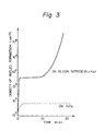
thin film 2 and Si, W, GaAs, InP, etc., as thethin film 3 to be deposited. - Fig. 3 is a graph showing the change with lapse of time of nucleation density (ND) on the deposited surface of SiO₂ and the deposited surface of silicon nitride.
- As shown in the same graph, soon after initiation of deposition, the nucleation density (ND) on SiO₂ is saturated at l0³ cm⁻² or less, and the value is not substantially changed even after 20 minutes.
- In contrast, on silicon nitride (Si₃N₄), it is once saturated at about 4 × l0⁵ cm⁻² or less and not substantially changed for 10 minutes thereafter, but is abruptly increased thereafter. This measurement example shows the case in which SiCl₄ gas is diluted with H₂ and deposited according to the CVD method under the conditions of a pressure of l70 Torr and a temperature of l000 °C.
- Such a phenomenon depends greatly on the difference in adsorption coefficient, release coefficient, surface diffusion coefficient, etc., relative to Si of the material surfaces of SiO₂ and silicon nitride, but the fact that SiO₂ itself is etched by the reaction of SiO₂ with Si atom itself to form silicon monooxide with higher vapor pressure, while no such etching phenomenon occurs on silicon nitride may be also considered to be a cause to effect selective deposition (T. Yonehara, S. Yoshioka, S. Miyazawa, Journal of Applied Physics 53, 6839, (l982)).
- Thus, by selecting SiO₂ and silicon nitride as the materials of the deposition surface and silicon as the material to be deposited, sufficiently great nucleation density difference (ΔND) as shown in the same graph can be obtained. Here, although SiO₂ is desirable as the material for the deposition surface, this is not limitative and sufficiently practical nucleation density difference (ΔND) can be obtained even by use of SiOx (0 < x < 2).
- Of course, the present invention is not limited to these materials, but the difference in nucleation density (ΔND) may be sufficiently l0³-fold or more in density of nuclei as shown by the same graph, and sufficient selective formation of deposited film can be done with the materials as exemplified below.
- As another method for obtaining this nucleation density difference (ND), ions of Si, N, etc., may be injected locally into the SiO₂ surface to form a region having excessive Si or N.
- The present invention utilizes selective deposition based on such nucleation density difference (ΔND) and, by forming a sufficiently minute region of a different kind of material having sufficiently greater nucleation density than the material of the deposition surface, so that a single nucleus may grow on the region, a single crystal is to be grown selectively only at the site where such fine different kind of material exists.
- In this connection, since selective growth of a single crystal is determined depending on the electron state of the crystal formation surface, particularly the state of dangling bonds, the material with higher nucleation density (for example, Si₃N₄) is not required to be a bulk material, but it may also be formed as a thin film on the surface of base plate of any desired material to form the above crystal formation surface.
- In the following, the present invention is described in detail by referring to the drawings.
- Figs. 4A - 4D are illustrations of the formation steps showing a first embodiment of the method for forming crystal according to the present invention, and Figs. 5A and 5B are perspective views corresponding to Figs. 4A and 4D.
- First, as shown in Fig. 4A and Fig. 5A, on the
substrate 4, athin film 5 non-nucleation surface (SNDS) with small nucleation density which enables selective deposition is formed and a material different from the material forming thethin film 5 with smaller nucleation density is deposited thinly, followed by patterning according to lithography, etc., to form sufficiently finely nucleation surface 6 (SNDL) (or called "Seed") comprising a different kind of material. However, the size, the crystal structure and the composition of thesubstrate 4 may be any desired ones, and a substrate having a functional device formed thereon prepared according to conventional semiconductor technique may be employed. Also, the nucleation surface (SNDL) 6 comprising a different kind of material is also inclusive of modified regions having excessive Si or N formed by ion injection of Si or N into thethin film 5 as described above. - Next, by selection of appropriate deposition conditions according to the FOCVD method, a crystalline deposited film is formed. That is, a single nucleus of a thin film material is firstly formed only on the nucleation surface (SNDL) 6. The size of the nucleation surface (SNDL) 6, which may differ depending on the kind of the material, may be several microns or less. Further, the nucleus grows while maintaining a single crystal structure to become a
single crystal grain 7 in shape of an island as shown in Fig. 4(B). For forming an island-shapedsingle crystal grain 7, it is desirable to determine the conditions so that no nucleation may occur at all on thethin film 5, as already mentioned. - The island-shaped
single crystal grain 7 further grows while maintaining the single crystal structure with the nucleation surface (SNDL) 6 as the center (lateral overgrowth), whereby it can cover over the whole surface of thethin film 5 as shown in the same Figure (C) (single crystal 7A). - Subsequently, if necessary, the
single crystal 7A is flattened by etching or polishing, and asingle crystal layer 8 capable of forming a desired device can be formed on thethin film 5 as shown in Fig. 4(D) and Fig. 5(B). - Thus, due to formation of the
thin film 5 for forming the non-nucleation surface (SNDS) on thesubstrate 4, any desired material can be used for thesubstrate 4 which is the supporting member. Further, in such a case, even when thesubstrate 4 may be one having a functional device, etc., formed thereon according to conventional semiconductor technique, thesingle crystal layer 8 can be easily formed thereon. - In the above embodiment, the non-nucleation surface (SNDS) is formed of
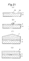
thin film 5, but a substrate comprising a material with small nucleation density (ND) enabling selective nucleation may be used as such and nucleation surfaces (SNDL) may be provided at any desired positions to form single crystal layers similarly thereon. - Figs. 6(A) - 6(D) are illustrations of the steps for forming crystal showing a second embodiment of the present invention. As shown in these figures, on a
substrate 9 comprising a material with small nucleation density (ND) enabling selective nucleation, the nucleation surface (SNDL) comprising a material with great nucleation density (ND) can be formed sufficiently minutely to form asingle crystal layer 8 similarly as in the first embodiment - Figs. 7(A) - 7(D) are illustrations of the formation steps showing a third embodiment of the method for forming crystal according to the present invention, and Figs. 8(A) and 8(B) are perspective views corresponding to Figs. 7(A) and 7(D).
- As shown in Fig. 7(A) and Fig. 8(A), on the amorphous insulating
substrate 11, with an interval of a distance ℓ, nucleation surfaces (SNDL) 12-1, 12-2, of a material different from thesubstrate 11 enabling the above selective nucleation are arranged sufficiently finely. The distance ℓ is set equal to the size of the single crystal region required for formation of semiconductor device or group of devices or greater. - Next, by selecting appropriate crystal forming conditions, on the nucleation surfaces (SNDL) 12-1, 12-2, only a nucleus of a crystal forming material is formed. That is, the nucleation surfaces 12-1, 12-2, are required to be formed to a sufficiently fine size (area) to the extent that only a single nucleus may be formed. The size of the nucleation surfaces (SNDL) 12-1, 12-2, which may be different depending on the kind of the material, may be several microns or less. Further, the nucleus grows while maintaining the single crystal structure, and become island-shaped single crystal grains 13-1, 13-2, as shown in Fig. 7(B). For forming island-shaped single crystal grains 13-1, 13-2, it is desirable to determine the conditions so that substantially no nucleation may occur at all on other surfaces than the nucleation surfaces (SNDL) on the
substrate 11. - The crystal direction in the normal line direction of the
substrate 11 of the island-shaped single crystal grains 13-1, 13-2 is determined so as to make the interface energy of the material of thesubstrate 11 and the material forming nucleus minimum. For, surface or interface energy has anisotropy depending on the crystal face. However, as already mentioned, the crystal direction within the substrate plane in amorphous substrate is not determined. - The island-shaped single crystal grains 13-1, 13-2 further grow to become
single crystals 13A-1, 13A-2, until the adjacentsingle crystals 13A-1, 13A-2, contact each other as shown in Fig. 7(C), but since the crystal directions within the substrate plane are not constant, acrystal grain boundary 14 is formed at the intermediate position between the nucleation surfaces (SNDL) 12-1 and 12-2. - Subsequently, the
single crystals 13A-1, 13A-2 grow three-dimensionally, but crystal faces with slow growth speed appear as the facet. For this reason, the surfaces ofsingle crystals 13A-1, 13A-2 are flattened by etching or polishing, and further the portion of thegrain boundary 14 is removed to form thin films of single crystals 15-1, 15-2,... containing no grain boundary in shape of lattices as shown in Fig. 7(D) and Fig. 8(B). The size of the single crystal films 15-1, 15-2, ... is determined by theinterval 1 between the nucleation surfaces (SNDL) 12A-1, 12A-2, as described above. That is, by determining appropriately the formation pattern of the nucleation surface (SNDL) 12A-1, 12A-2, the position of the grain boundary can be controlled to form single crystals with desired sizes at a desired arrangement - Fig. 9(A)-(D) are illustrations of the formation steps of crystal showing a fourth embodiment of the present invention. As shown in these Figures, similarly as described in the first embodiment on a desired
substrate 4 is formed a thin film non-nucleation surface (SNDS)5 comprising a material with small nucleation density (ND) enabling selective nucleation is formed, and nucleation surfaces (SNDL)12 comprising a different kind of material with greater nucleation density (ND) are formed with an interval ℓ thereon, and asingle crystal layer 15 can be formed in the same manner as in the above third embodiment. - Figs. 10(A) - 10(C) are illustrations of the formation steps showing a fifth embodiment of the method for forming crystal according to the present invention, and Figs. 11(A) and 11(B) are perspective views of the substrates in Figs. 10(A) and 10(C).
- First, as shown in Fig. 10(A) and Fig. 11(A),
concavities 16 with desired size and shape are formed on the amorphous insulatingsubstrate 11, and nucleation surfaces (SNDL) 12 with sufficiently fine size for forming only single nucleus are formed therein. - Subsequently, as shown in Fig. 10(B), island-shaped
single crystal grains 13 are grown similarly as in the first embodiment. - And, as shown in Fig. 10(C) and Fig. 11(B),
single crystal grains 13 are grown until embedding theconcavity 16 to form asingle crystal layer 17. - In this embodiment, since
single crystal grains 13 grow within theconcavity 16, the steps of flattening and removing the grain portion may be unnecessary. - Fig. 12(A)-(C) are illustrations of the formation steps of crystal showing a sixth embodiment of the present invention. As shown in these Figures, on any desired
substrate 4 similarly as in the first embodiment, a thin film non-nucleation surface (SNDS) 18 comprising a material with small nucleation density(ND) enabling selective nucleation is formed, andconcavities 16 with desired size and shape are formed thereon. and, within the concavities are formed minutely nucleation surfaces (SNDL)12 comprising a material with greater nucleation density (ND) which is different from the material forming the nonnucleation surface (SNDS), and single crystal layers 17 are formed in the same manner as in the fifth embodiment. - Fig. 13(A)-(C) are illustrations of the formation steps of crystal showing a seventh embodiment of the present invention. After formation of concavities on a desired substrate, a thin film nonnucleation surface (SNDS)20 comprising a material with sufficiently small nucleation density (ND) enabling selective nucleation is formed, and following the same procedure as in the above embodiments, single crystal layers 17 can be formed.
- Fig. 14 is a schematic sectional view showing an example of the semiconductor electronic device with a multi-layer structure produced by use of the first embodiment of the present invention.
- In Fig. 14 on the
semiconductor substrate 1401 such as Si or GaAs,transistors 1402 or other semiconductor devices or optical devices are formed, andSiO₂ layer 1403 having a surface for formation of, for example, nonnucleation surface (SNDS) 1404 is formed thereon according to the CVD method or the sputtering method. And, as already mentioned, athin film 1406 having nucleation surfaces (SNDL) 1405 having sufficiently minute areas so that only a single nucleus are formed of, for example, Si₃N₄, and a single crystal is grown from said nucleation surface (SNDL) 1405 to form an Sisingle crystal layer 1407. - Subsequently, on the
single crystal layer 1407 are formed transistors 1408 or other semiconductor devices or optical devices, and the devices formed respectively on thesubstrate 1401 and the Sisingle crystal layer 1407 are electrically connected through theSiO₂ layer 1403. Thus, for example, by forming thetransistor 1402 of the first layer (substrate 1401) and the transistor 1408 of the second layer (single crystal layer 1404) respectively as the MOS transistors, and connecting these to form CMOS, a CMOS entirely free from mutual interaction can be produced. Also, according to the technique as described above, an electroluminescent device can be also formed integrated with its driving circuit to accomplish a high degree of integration. - Further, by repeating this embodiment,
single crystal layers 1407 can be formed in many layers withSiO₂ layer 1403 sandwiched therebetween, whereby a semiconductor electronic device with a multiple structure can be formed easily. - Figs. 15(A)-15(D) are illustrations of the steps for forming crystal showing an eighth embodiment of the present invention.
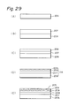
- Figs. 15(A)-15(C) are the same as Figs. 7(A) - 7(C). That is, a plurality (two in the figure) of nucleation surfaces 12 are formed with an interval of ℓ, and
single crystal grains 13 subjected to overgrowth on the nucleation surfaces 12 are formed. By permitting thesingle crystal grains 13 to further grow to formsingle crystals 13A, agrain boundary 14 is formed approximately at the center between the nucleation surfaces (SNDL) 12, and by flattening the surface ofsingle crystal 13A, apolycrystalline layer 21 with regular grain sizes which are approximately equal to ℓ as shown in Fig. 15(D) can be obtained. - Since the grain size of the
polycrystalline layer 21 is determined by the interval ℓ between the nucleation surfaces (SNDL) 12, it becomes possible to control the grain size of the polycrystal. In the prior art, the grain size of a polycrystal was changed by a plural number of factors such as the formation method, formation temperature, etc., and also when preparing a polycrystal with large grain size, it had a grain size distribution with a considerable width. However, according to the present invention, the grain size and grain size distribution can be determined with good controllability by the interval ℓbetween the nucleation surfaces 12. - Of course, as shown in Fig. 9, the
above polycrystal layer 21 may be formed by forming a non-nucleation surface (SNDS) 5 with small nucleation density (ND) on a desiredsubstrate 4 and nucleation surfaces (SNDL) 12-1, 12-2 with greater nucleation density (ND). In this case, as already mentioned, the substrate material and structure are not limited, but thepolycrystal layer 21 can be formed by controlling the grain size and the grain size distribution. - Next, the specific method for forming a single crystal layer or a polycrystal layer in the above respective embodiments is described in more detail by referring primarily to the third embodiment shown in Fig. 7 and the eighth embodiment shown in Fig. 15.
- By thermal oxidation of an Si single crystal wafer to form an SiO₂ layer on the surface, a
substrate 11 is obtained with its surface being formed into non-nucleation surface (SNDS). Of course, a quartz substrate which is a material with small nucleation density (ND) can be also used as thesubstrate 11, or alternatively non-nucleation surface (SNDS) may be provided by forming SiO₂ layer on the surface of any desired base substrate such as metal, semiconductor, magnetic material, piezoelectric material, insulator, etc., by use of the sputtering method, the CVD method, the vacuum vapor deposition method, etc. Also, as the material forming non-nucleation surfaces (SNDS), SiO₂ is desirable, but SiOx (0 < x < 1) with the value of x being varied may be also employed. - On the SiO₂ layer of the
substrate 11 having SiO₂ layer thus formed on the surface is deposited as silicon nitride layer (e.g. Si₃N₄ layer) or a polycrystalline silicon layer according to the reduced pressure chemical vapor deposition method, and subsequently the silicon nitride layer or polycrystalline silicon layer is subjected to patterning according to conventional lithographic technique or lithographic technique by use of X-ray, electron beam or ion beam, whereby nucleation surface (SNDL) 12 having fine area of preferably 10 µm or less, more preferably several micron or less, optimally about 1 µm or less. - Subsequently, for example, by the selective use of a suitable gas among the abovementioned gases and according to the FOCVD method, for example an Si single crystal is selectively grown on the
above substrate 11. - In this procedure, the substrate temperature, pressure, etc., may be conveniently determined, but the substrate temperature may be preferably 100 to 600 °C.
- Within a time of about some 10 minutes, by selection of optimum growth conditions,
grains 13 of single crystals of Si grow on the nucleation surfaces (SNDS) 12 comprising silicon nitride layer or polycrystalline silicon layer on the SiO₂ layer as the center, and grow to sizes of some 10 µm or more. - Subsequently, by the reactive ion etching (RIE) method utilizing the etching speed difference between Si and SiO₂, the surfaces of the
single crystals 13A are flattened by selective etching of only Si, whereby apolycrystalline silicon layer 21 controlled in grain size can be formed (Fig. 15(D)). Further, by removing the grain boundary portion, island-shaped single crystalline silicon layers 15-1, 15-2 are formed (Fig. 7(D)). If unevenness on the surface of thesingle crystal grains 13A-1, 13A-2 are large, mechanical polishing may be conducted before etching. - When electrical field effect transistors are formed according to conventional semiconductor device preparation technique on the single crystal silicon layers 15 thus formed with a size of some 10 µm or more containing no grain boundary, characteristics not inferior to that formed on single silicon wafer are exhibited.
- Also, mutual interference between the adjacent single crystal silicon layers can be prevented, if they are electrically separated by an electrical insulator such as SiO₂, even if a complementary type electrical field effect transistor (C-MOS) may be constituted.
- Also, since the thickness of the active layer of the device formed is thinner than the case when employing Si wafer, there is no erroneous actuation by the charges generated when radiation is irradiated. Further, due to lowering in unwanted capacity, speed-up of the device can be effected. Also, since any desired substrate can be used, a single crystal layer can be formed on a substrate of large area at lower cost than when employing Si wafer. Further, since a single crystal layer can be formed also on other semiconductors, piezoelectric materials, dielectric materials, etc., a multi-functional three-dimensional integrated circuit can be realized. Thus, the present invention exhibits a number of excellent effects.
- For obtaining sufficient nucleation density difference (ΔND) between the material (MS) for formation of non-nucleation surface (SNDS) and the material (ML) for formation of nucleation surface (SNDL) as described above, for polycrystalline silicon or SiO₂ as the material for formation of non-nucleation surface (SNDS) to be used in combination, the material for formation of nucleation surface (SNDL) is not limited to Si₃N₄, but silicon nitrides with various chemical composition ratios may be employed.
- The chemical composition ratio of silicon nitride may be varied e.g. as follows.
- In the plasma CVD method for forming silicon nitride film at low temperature by decomposition of SiH₄ gas and NH₃ gas in RF plasma, by varying the flow rate ratio of SiH₄ gas and NH₃ gas, the composition ratio of Si and N in the deposited silicon nitride film can be varied to a great extent.
- Fig. 16 is a graph showing an example of the relationship between the flow rate ratio of SiH₄ and NH₃ and the composition ratio of Si and N in the silicon nitride film formed.
- The deposition conditions at this time were RF output of 175 W, substrate temperature of 380 °C and the flow rate of NH₃ gas was varied with the SiH₄ gas flow rate being fixed at 300 cc/min. As shown in the same graph, by varying the gas flow rate ratio of NH₃/SiH₄ from 4 to 10, the Si/N ratio in the silicon nitride film was found to be varied from 1.1 to 0.58 according to Auger's electron spectrophotometry.
- On the other hand, the composition of the silicon nitride film formed according to the reduced pressure CVD method by introducing SiH₂Cl₂ gas and NH₃ gas under the conditions of a reduced pressure of 0.3 Torr and a temperature of about 800 °C was found to be Si₃N₄ (Si/N = 0.75) which is approximately the stoichiometric ratio.
- Also, the silicon nitride film formed by heat treatment of Si at about 1200 °C in ammonia or N₂ (hot nitrification method) can be obtained with a composition further approximate to the stoichiometric ratio, since the formation method is performed under thermal equilibrium.
- By use of silicon nitrides formed by the various methods as described above as the material for forming nucleation surface (SNDL) with higher nucleation density than SiO₂, the above nucleus of Si can be grown on the nucleation surface (SNDL) comprising silicon nitride to form Si single crystal based on the nucleation density (ΔND) corresponding to the chemical composition ratio of silicon nitride.
- Fig. 17 is a graph showing the relationship between Si/N composition ratio and nucleation density (ND). As shown in the same graph, by varying the chemical composition ratio of the silicon nitride film, the nucleation density of the Si single crystal nucleus formed thereon changes to a great extent The nucleation conditions in the graph shown in Fig. 17 correspond to the case when Si single crystal nucleus was formed by reacting SiCl₄ gas reduced to 175 Torr with H₂ at 1000°C. Of course, another graph will be obtained if nucleation conditions such as gas species, pressure, temperature, etc., are changed.
- The phenomenon that the nucleation density thus changes according to the chemical composition ratio of silicon nitride affects the size (area) of the nucleation surface (SNDL) when employing silicon nitride as the material for forming the nucleation surface (SNDL) which is formed sufficiently finely to the extent that a single nucleus may be grown. That is, when employing silicon nitride having a composition with great nucleation density (ND) only a single crystal can be formed on the nucleation surface (SNDL) by forming the nucleation surface (SNDL) extremely finely as compared with the silicon nitride with relatively smaller nucleation density (ND).
- Such a point is applicable as a similar tendency for other materials for forming nucleation surface (SNDL).
- Accordingly, in the present invention, for accomplishing its objects effectively, it is desirable to select a nucleation density (ND) and a size of nucleation surface (SNDL) formed of silicon nitride, etc., capable of forming only a single crystal suitably as desired. For example, under the nucleation condition for obtaining a nucleation density (ND) of about 10⁵ cm⁻², it is possible to form selectively only a single nucleus, if the size of the nucleation surface (SNDL) comprising silicon nitride is about 4 µm or less. The Si/N ratio in that case is about 0.5. .
- As another method for realizing nucleation density difference (ΔND) when forming Si single crystal nucleus, ion injection of Si, N, P, B, F, Ar, He, C, As, Ga, Ge, etc., may be effected locally onto the SiO₂ surface which is a material for forming non-nucleation surface (SNDS) with smaller nucleation density to form a modified region with a desired size on the surface of the SiO₂ layer, and utilize this modified region as the nucleation surface (SNDL) with greater nucleation density (ND).
- For example, the SiO₂ layer surface is covered with a photoresist layer and the desired portions are exposed, developed, and dissolved to have the SiO₂ layer surface exposed.
- Subsequently, by use of SiF₄ gas as the source gas, Si ions are implanted onto the SiO₂ layer surface portion exposed at 10 keV at a density of 1 × 10¹⁶ - 1 × 10 ¹⁸ cm⁻². The projected flying distance in this case is 114 Å, and the Si concentration on the exposed surface of SiO₂ layer reaches about 10²² cm⁻³. Since the SiO₂ layer is originally amorphous, the modified region made excessively enriched in Si by injection of Si ions is also amorphous.
- For formation of a modified region, ion injection can be effected with the use of a resist as the mask, but it is also possible to inject a narrowed Si ion beam selectively at a desired position on the SiO₂ layer surface within a desired area without use of a resist mark by use of converged ion beam technique.
- After having thus effected Si ion injection, by peeling of the resist on the remaining portion, Si excessive modified region is formed in the SiO₂ layer surface portion at a desired position with a desired size. On the modified region of the SiO₂ layer surface portion having such modified region formed, Si single crystal is permitted to grow in vapor phase.
- Fig. 18 is a graph showing the relationship between the injected amount of Si ions and the nucleation density (ND).
- As shown in the same graph, it can be understood that nucleation density (ND) is increased as the Si⁺ injected amount is more.
- Therefore, by forming this modified region sufficiently finely, only single nucleus of Si can be permitted to grow with this modified region as the nucleation surface (SNDL), whereby a single crystal can be grown as described above.
- Formation of the modified region to a sufficiently fine size to the extent for growth of only a single nucleus can be accomplished easily by patterning of a resist, or narrowing of the beam of converged ion beam.
- Figs. 19(A) - 19(D) are illustrations of the formation steps showing a 9th embodiment of the method for forming crystal according to the present invention, and Figs. 20(A) and 20(B) are perspective views corresponding to Figs. 19(A) and 19(D).
- First, as shown in Fig. 19(A) and Fig. 20(A), on the
base substrate 4 is formed a thin film 6 (or called "Seed") [ forming nucleation surface (SNDL)6A ] with greater nucleation density enabling selective nucleation, on which a material different from the material forming thethin film 6 with greater nucleation density is thinly deposited, followed by patterning according to lithography, etc., to form athin film 5 comprising a different material and forming nonnucleation surface (SNDS)5A so as to provide sufficiently finely nucleation surfaces (SNDL)6A. However, the size, the crystal structure, and composition of thebase substrate 4 may be chosen as desired, and it may be also a substrate having a functional device prepared according to conventional semiconductor technique formed thereon. Also, the nucleation surface (SNDL)6A comprising a different material may be also formed as a modified region containing excessive Si, N or the like which may be formed by forming athin film 6 beneath the SiO₂thin film 5 of a polycrystalline silicon or SiO₂, and injecting ions of Si, N or the like into the exposedportions 6A. - Next, by selection of appropriate desposition conditions, a single nucleus of a crystal formation material is formed only on the nucleation surface (SNDL)6A. That is, the nucleation surface (SNDL)6A is required to be formed sufficiently minutely so that only a single nucleus may be formed thereon. The size of the nucleation surface (SNDL)6A, which may differ depending on the kind of the material, may be several microns or less. Further, the nucleus grows while maintaining a single crystal structure to become a
single crystal grain 7 in shape of an island as shown in Fig. 19(B). For forming an island-shapedsingle crystal grain 7, it is desirable to determine the conditions so that no nucleation may occur at all on thethin film 5A, as already mentioned. - The island-shaped
single crystal grain 7 further grows while maintaining the single crystal structure with the nucleation surface (SNDL)6A as the center (lateral over growth), whereby it can cover over the whole surface of thethin film 5 as shown in Fig. 19(C) (single crystal 7A). - Subsequently, if necessary, the single crystal 7a is flattened by etching or polishing, and a
single crystal layer 8 capable of forming a desired device can be formed on thethin film 5 as shown in Fig. 19(D) and Fig. 20(B). - Thus, due to formation of the
thin film 6 forming the nucleation surface (SNDL)6A on thesubstrate 4, any desired material can be used for thesubstrate 4 which is the supporting member. Further, in such a case, even when thesubstrate 4 may be one having a functional device etc., formed thereon according to conventional semiconductor technique, thesingle crystal layer 8 can be easily formed thereon. - In the above embodiment, the nucleation surface (SNDL)6A is formed of
thin film 6, but a substrate comprising a material with large nucleation density (ND) enabling selective nucleation may be used as such and non-nucleation surfaces (SNDS) may be provided at any desired positions to form single crystal layers similarly thereon as shown in Fig. 21. - Figs. 21(A) - 21(D) are illustration of the steps for forming crystal showing a second embodiment of the present invention. As shown in these figures on a
substrate 9 comprising a material with large nucleation density (ND) enabling selective nucleation, athin film 5 forming the non-nucleation surface (SNDS)5A which comprises a material with small nucleation density (ND) can be formed so as to give exposed portions of thesubstrate 9 as nucleation surface (SNDL)9A sufficiently minutely to form asingle crystal layer 8 by the use of said substrate similarly as in the first embodiment. - Figs. 22(A) - 22(D) are illustrations of the formation steps showing a 11th embodiment of the method for forming crystal according to the present invention, and Figs. 23(A) and 23(B) are perspective views corresponding to Figs. 22(A) and 22(D).
- As shown in Fig. 22(A) and Fig. 23(A), on an
appropriate base substrate 10 such as glass substrate, etc., an amorphous insulatingthin film 12 with relatively greater nucleation density (ND) such as Si₃N₄, etc., is provided, and on saidthin film 12 is formed selectively athin film 11 at a desired position with a different material having smaller nucleation density relative to the material forming thethin film 12 which enables the above selective nucleation with an interval of a distance ℓ, thereby arranging nucleation surfaces (SNDL)12A-1, 12A-2 with sufficiently small areas so as to form only single nucleus thereon. This distance ℓ may be set at a size which is equal to or greater than the size of the single crystal region required for formation of a semiconductor device or a group of devices. - Next, by selecting appropriate crystal forming conditions, on the nucleation surfaces (SNDL)12A-1, 12A-2 only a nucleus of a crystal forming material is formed. That is, as described above, the nucleation surfaces 12A-1, 12A-2 are required to be formed to a sufficiently fine size (area) to the extent that only a single nucleus may be formed. The size of the nucleation surfaces (SNDL)12A-1, 12A-2, which may be different depending on the kind of the material, may be several microns or less. Further, the nucleus formed as above grows while maintaining the single crystal structure, and become island-shaped single crystal grains 13-1, 13-2 as shown in Fig. 22(B). For forming island-shaped single crystal grains 13-1, 13-2, it is desirable to determine the conditions so that substantially no nucleation may occur at all on other surfaces than the nucleation surfaces (SNDL)12A-1, 12A-2 [ non-nucleation surface (SNDS)11A ].
- The crystal direction in the normal line d direction of the
thin film 12 of the island-shaped single crystal grains 13-1, 13-2 is determined so as to make the interface energy of the material of thefilm 12 and the material forming nucleus minimum. For, surface or interface energy has anisotropy depending on the crystal face. However, as already mentioned, the crystal direction within the surface plane in amorphous surface is not determined. - The island-shaped single crystal grains 13-1, 13-2 further grow to become
single crystals 13A-1, 13A-2 until the adjacentsingle crystals 13A-1, 13A-2 contact each other as shown in Fig. 22(C), but since the crystal directions within the substrate plane vary from one single crystal to another, acrystal grain boundary 14 is formed at the intermediate position between the nucleation surfaces (SNDL) 12-1 and 12-2. - Subsequently, the
single crystals 13A-1, 13A-2 grow three-dimensionally, but crystal faces with slow growth speed appear as the facet. For this reason, the surfaces ofsingle crystals 13A-1, 13A-2 are flattened by etching or polishing, and further the portion of thegrain boundary 14 is removed to form thin films of single crystals 15-1, 15-2, ... containing no grain boundary in shape of lattices as shown in Fig. 22(D) and Fig. 23(B). The size of the single crystal films 15-1, 15-2, ... is determined by theinterval 1 between the nucleation surfaces (SNDL)12A-1, 12A-2 as described above. That is, by determining appropriately the formation pattern of the nucleation surface (SNDL) 12A-1, 12A-2, the position of the grain boundary can be controlled to form single crystal with desired sizes at a desired arrangement. - Figs. 24(A) - 24(C) are illustrations of the formation steps showing a 12th embodiment of the method for forming crystal according to the present invention, and Figs. 25(A) and 24(B) are perspective views of the substrates in Figs. 24(A) and 24(C).
- First, as shown in Fig. 24(A) and Fig. 25(A), similarly as shown in the step (A) in Fig. 7,
thin film base substrate 10 to form nucleation surfaces (SNDL)12A-1, 12A-2 and non-nucleation surface (SNDS)11A. Subsequently, so that concavities 14-1, 14-2 with desired sizes and shapes may be provided at the corresponding positions to the nucleation surfaces (SNDL) 12A-1, 12A-2, a thin film 11-1 is formed with same material as the thin film 11a or a material having nucleation density equal to or smaller than said material. Thus, a substrate for formation of crystal having nucleation surfaces (SNDL)12A-1, 12A-2 with sufficiently fine sizes for forming only single nucleus within concavities 14-1, 14-2 is formded. - Subsequently, as shown in Fig. 24(B), island-shaped single crystal grains 13-1, 13-2 are grown similarly as in the first embodiment.
- And, as shown in Fig. 24(C) and Fig. 25(B), single crystal grains 13-1, 13-2 are grown until embedding the concavity 14-1, 14-2 to form a single crystal layer 15-1, 15-2.
- In this embodiment, since single crystal grains 13-1, 13-2 grow within the concavity 14-1, 14-2, the steps of flattening and remoing the grain portion may be unnecessary.
- Figs. 26(A) - 26(D) are illustrations of the steps for forming crystal showing a 13th embodiment of the present invention.
- Figs. 26(A) - 26(C) are the same as Figs. 22(A) - 22(C). That is, a plurality (two in the Figure) of nucleation surfaces 12A-1, 12A-2 are formed with an interval of ℓ, and single crystal grains 13-1, 13-2 subjected to over growth on the nucleation surfaces 12A-1, 12A-2 are formed. By permitting the single crystal grains 13-1, 13-2 to further grow to form
single crystals 13A-1, 13A-2, agrain boundary 14 is formed approximately at the center between the non-nucleation surfaces (SNDS)11A, and by flattening the surface ofsingle crystal 13A-1, 13A-2, apolycrystalline layer 16 with regular grain sizes which are approximately equal to ℓ as shown in Fig. 12(D) can be obtained. - Since the grain size of the
polycrystalline layer 16 is determined by the interval ℓ between the nucleation surfaces (SNDL) 12A-1, 12A-2, it becomes possible to control the grain size of the polycrystal. In the prior art, the grain size of a polycrystal was changed by a plural number of factors such as the formation method, formation temperature, etc., and also when preparing a polycrystal with large grain size, it had a grain size distribution with a considerable width. However, according to the present invention, the grain size and grain size distribution can be determined with good controllability by the interval ℓ between the nucleation surfaces (SNDL)12A-1, 12A-2. - Of course, as shown in Fig. 21, a polycrystal layer may be formed as above by forming a
thin film 5 having a non-nucleation surface (SNDS)5A with small nucleation density (ND) on a desiredsubstrate 9 and plural nucleation surfaces (SNDL)9A with greater nucleation density (ND) at desired positions and intervals. In this case, as already mentioned, the substrate material and structure are not limited, provided that the nucleation density difference (ΔND) is taken into consideration, but the polycrystal layer can be formed by controlling the grain size and the grain size distribution. - Next, the present invention is described by referring to a typical example of the apparatus for forming a deposited film according to the process of the present invention.
- Fig. 27 is a partial sectional view showing schematic construction of an example of the device for forming deposited film in which the process of the present invention is practiced.
- In Fig. 27, 101 is a deposition chamber (film forming space) in which deposition of silicon thin film is effected, and the
deposition chamber 101 is internally connected to an evacuation system not shown through anevacuation outlet 106, whereby thedeposition chamber 101 can be maintained at a desired pressure. In thedeposition chamber 101, there are provided a set of the introducingpipe 102 for radicals (SX) containing e.g., silicon and a halogen which is the active species (A) and the introducingpipe 103 for e.g., hydrogen radicals as active species (B), respectively. The tips of the respective radical introducing pipes are thick at the actingchambers outlets deposition chamber 101, asubstrate supporting member 104 is held by theroller 110 so as to be movable reciprocally in the direction perpendicular to the paper surface. And on said supportingmember 104 is held asupport 105 for deposition. The respective radicals coming out from theoutlet deposition chamber 101 to form a film on thesubstrate 105. The radicals (SX) and hydrogen radicals are formed from the respective starting material gases in the active species forming chambers such as heating furnaces or plasma chambers, etc., not shown, respectively, and thereafter introduced through the introducingpipes chambers -
Roller 110 is provided only for depositing silicon thin film over the whole surface of the substrate by moving thesubstrate 105. - The introducing
pipe 111 is an introducing pipe for another gas having chemical or physical etching activity (etching gas), and in some cases the etching gas is previously activated in the heating furnace or plasma furnace not shown and led to theoutlet 114. From theoutlet 114, the etching gas for attacking the film is released to cut or exclude selectively the bonds except in the growth direction of the characteristics of the film. Introduction of the etching gas, other than through such separate introduction pipes, can be also done through theintroduction pipes - The present invention is described in more detail by referring to Examples.
- By means of the film forming device shown in Fig. 27, a deposited film according to the method of the present invention was prepared as described below.
- The
substrate 118 was prepared according to the steps shown in Fig. 28. First, apolycrystalline silicon substrate 201 as shown in Fig. 28(A) was washed and then a thinsilicon oxide film 202 was deposited on the whole surface of thesubstrate 201 according to the sputtering method (in this case, other than the sputtering method, various thin film deposition method, MBE method, CVD method, etc., may be employed). [Fig. 28(B)]. - Subsequently, an electron beam resist
layer 203 was applied on the thin film 202 [-Fig. 28(C)], and the electron beam resistlayer 203 was exposed to light by use of a photomask with a desired pattern, and the electron beam resistlayer 203 was partially removed by development [Fig. 28(D)]. - With the residual electron beam resist 203A as the mask, the silicon oxide
thin film 202 was etched to form a thin film 202A having a desired pattern [Fig. 28(E)]. - According to the steps as described above, a
substrate 118 with certain crystal face of the polycrystalline silicon 201A being exposed at constant intervals from the silicon oxide film was obtained. - The regions of the silicon crystals exposed on the surface of the
substrate 118 has a diameter of 3 µm and an interval of 15 µm. - Next, by use of the device shown in Fig. 27, a crystalline silicon thin film was formed on the
above substrate 118. - First, by use of Si₂F₆ as the starting gas for formation of radicals containing silicon and halogen, it was permitted to flow at a flow rate of 100 SCCM into the reaction furnace maintained at 800 °C to be decomposed therein, followed by release through the introducing
pipe 102 into the actingchamber 108. At the same time Ar gas was permitted to flow through the introducingpipe 111 at a rate of 150 SCCM, and a microwave of 2.45 GHz was introduced at a power of 1.0 w/cm² into said introducingpipe 103 to effect discharging and decompose H₂, followed by release of the decomposed gas into the activatingchamber 108 at a flow rate of 25 SCCM. The substrate temperature was maintained at 330 °C and the pressure at 0.2 Torr. Thus yielding a deposited film of about 12 µm thick. - Fig. 28(F) shows schematically the crosssection of the crystalline silicon deposited
film 205 obtained on thesubstrate 118. - The size of the
crystal grain 204 was determined so that thecrystal grain bounderies 205 became equidistant from the exposed portions 201A of thecrystal substrate 201 at which thesilicon oxide layer 202 was removed. - Next, when crystallinity of the silicon deposited film was evaluated according to the X-ray diffractometry and electron beam diffractometry by use of respective samples obtained. they were confirmed to be polycrystalline silicon films. Further, the grain size of the polycrystalline silicon determined by the Scherrar method was about 25±2 µm. The variance in crystal grain size was substantially negligible over the whole substrate.
- Also, when the surface state of the sample was observed by a scanning type electron microscope, the smoothness was found to be good without wavy pattern, etc., and the film thickness irregularity was ±4% or less.
- Also, when the mobility and electroconductivity of the crystalline Si deposited film of the sample prepared were measured according to the Van der Pauw method, they were found to be 300 (cm/V·sec) and 9 × 10⁻⁶ (S·cm⁻¹), respectively.
- The
substrate 118 was prepared according to the steps shown in Fig. 29. - First, a
glass substrate 201 comprising substantially uniform composition material as shown in Fig. 29(A) was washed and then according to the thermal CVD method amorphous SiN(A-SiN)thin film 202 was formed with a thickness of about 2µm on the whole surface of the substrate 201 [Fig. 29(B)]. - Subsequently, surface annealing of the above A-SiN
thin film 202 was effected in N₂ atmosphere by means of a laser annealing device on the above A-SiNthin film 202 to form a crystalline Si (C-Si₃N₄) 203 on the surface layer of the A-SiN thin film 202 (to the depth of about 1 µm) [Fig. 29(C)]. - At this time, the laser was irradiated with Ar-CW laser of 4880 Å, at a scanning speed of 2.5 cm/sec and at an energy of 10 W. Subsequently, the surface of the C-
Si layer 203 was scanned by means of the above laser annealing device in O₂ atmosphere to form selectively the SiO₂ layer 204 [Fig. 29(D)]. - According to the steps as described above, the
substrate 118 having C-Si₃N₄ layer 203A exposed at constant intervals with other portions being covered withSiO₂ layer 204 was formed. The domains of C-Si₃N₄ layer 203A exposed on the substrate surface were about 4 µm in diameter with intervals of 3 µm. - Further, by use of this
substrate 118, crystalline silicon was deposited by means of the device shown in Fig. 27 similarly as described in Example 1. Deposition conditions were the same as in Example 1 except that the pressure was set at 0.1 Torr and the substrate temperature at 270°C. - Fig. 29(E) is a schematic drawing showing the cross-section of the crystalline silicon deposited
film 205 obtained on thesubstrate 118. - The size of the crystal grain was determined so that the
crystal grain boundary 206 was at the same distance from the exposed portions 203A of thecrystalline substrate 201 other than theSiO₂ layer 204. - When crystallinity of the silicon deposited film was evaluated according to the X-ray diffractometry and electron beam diffractometry by use of respective samples obtained, they were confirmed to be polycrystalline silicon films. Further, the grain size of the polycrystalline silicon determined by the Scherrar method was 20±0.5 µm. The variance in crystal grain size was substantially negligible over the whole substrate.
- Also, when the surface state of the sample was observed by a scanning type electron microscope, the smoothness was found to be good without wavy pattern, etc., and the film thickness irregularity was ±4% or less. Also when the mobility and electroconductivity of the crystalline Si deposited film of the sample prepared were measured according to the Van der Pauw method, they were found to be 150 (cm/V·sec) and 5×10⁻⁶ (S·cm⁻¹), respectively.
- By use of the same conditions as in samples Nos. 1 and 2 in Examples 1 and 2, a thin film transistor (hereinafter abbreviated as TFT) as shown in Fig. 31 was prepared. After deposition of a Si
semiconductor polycrystalline layer 3002 as shown in Fig. 30 with a film thickness of 0.5 µm on a glass (Corning #7059)base plate 3001 subjected to patterning with SiNH under the above conditions, TFT was prepared by use of the process for preparation of the upper gate coplanar TFT. - First, according to the glow discharge method, an n⁺ layer (specific resistivity σ ≃ 1Ω·cm) which is the
ohmic contact layer 3103 doped with P was formed to a thickness of 1000 Å, and then anactive layer 3102 was remained by photolithography, followed by etching of thechannel portion 3106 to form theabove contact layer 3103. Then, by use of the glow discharge method, NH₃ and SiH₄ were decomposed to deposit a Si-N-H film with a film thickness of 3000 Å, dielectric constant of 67 and adielectric strength 3 × 10⁶ V/cm, VFB ≃ OV at a substrate temperature of 200 °C. Then contactholes 3105 for source and drain were opened, Al was deposited to 5000 Å by vacuum vapor deposition as the upper electrode, and thesource electrode 3107, thegate electrode 3109 and thedrain electrode 3108 were respectively formed by photolithography. The gate width W and the gate length L were respectively 650 µ and 22 µ. The characteristics when the drain electrode was earthed and various ⊕ voltages were applied on the source electrode and the gate electrode were measured. In the drain current ID - drain voltage VD characteristic, good saturation characteristics were obtained in both Nos. 1 and 2 to give a high current of 7 × 10⁻⁴ A at a gate voltage of 10 V and a drain voltage of 10 V. The TFT characteristics obtained from the results of measurement of the drain current ID at various gate voltage VD are shown in Table 1. - The TFT by use of the film as obtained above was found to have good characteristics.

- The method for forming deposited film of the present invention can form a deposited film only by contacting an activated species (A) with an activated species (B), and has the advantage of requiring particularly no reaction exciting energy from the outside. Accordingly, it becomes possible to lower the substrate temperature. Also, since a material which becomes the crystal nucleus for the deposited film or capable of forming selectively the crystal nucleus can be arranged at a desired position on the substrate surface, any desired polycrystalline or single crystalline deposited film with extremely high orientation and great grain size can be formed. Further, simultaneously with saving of energy, it is possible to obtain a crystalline deposited film having uniform film quality and characteristics over a large area with easy management of the film quality. Further, a crystalline film excellent in productivity, bulk productivity and having high quality with excellent electrical, optical semiconductive and other physical properties can be obtained with ease.
Claims (33)
arranging said substrate within a film forming space; and then
introducing an active species (A) formed through decomposition of a compound containing silicon and a halogen and an active species (B) formed from a chemical substance for film formation having a property of effecting chemical mutual reaction with said active species (A) into the film forming space wherein said substrate is previously arranged, thus resulting in formation of a single nucleus on said nucleation surface (SNDL) followed by single crystal growth from said nucleus.
Applications Claiming Priority (4)
| Application Number | Priority Date | Filing Date | Title |
|---|---|---|---|
| JP83930/86 | 1986-04-11 | ||
| JP8393086 | 1986-04-11 | ||
| JP85516/87 | 1987-04-06 | ||
| JP62085516A JP2692804B2 (en) | 1986-04-11 | 1987-04-06 | Method of forming crystalline deposited film |
Publications (3)
| Publication Number | Publication Date |
|---|---|
| EP0241316A2 true EP0241316A2 (en) | 1987-10-14 |
| EP0241316A3 EP0241316A3 (en) | 1988-09-21 |
| EP0241316B1 EP0241316B1 (en) | 1998-07-22 |
Family
ID=26424966
Family Applications (1)
| Application Number | Title | Priority Date | Filing Date |
|---|---|---|---|
| EP87303224A Expired - Lifetime EP0241316B1 (en) | 1986-04-11 | 1987-04-13 | Method for forming crystalline deposited film |
Country Status (5)
| Country | Link |
|---|---|
| EP (1) | EP0241316B1 (en) |
| AT (1) | ATE168821T1 (en) |
| AU (2) | AU7143987A (en) |
| CA (1) | CA1329756C (en) |
| DE (1) | DE3752203T2 (en) |
Cited By (8)
| Publication number | Priority date | Publication date | Assignee | Title |
|---|---|---|---|---|
| FR2645178A1 (en) * | 1989-03-31 | 1990-10-05 | Canon Kk | PROCESS FOR FORMING CRYSTALLINE FILM |
| EP0412755A1 (en) * | 1989-08-07 | 1991-02-13 | Canon Kabushiki Kaisha | Method of forming crystal semiconductor film |
| EP0472452A1 (en) * | 1990-08-24 | 1992-02-26 | Thomson-Csf | Power transistor and its manufacturing process |
| EP0509452A1 (en) * | 1991-04-15 | 1992-10-21 | Canon Kabushiki Kaisha | Light emitting device having stepped non-nucleation layer |
| US5278092A (en) * | 1989-08-07 | 1994-01-11 | Canon Kabushiki Kaisha | Method of forming crystal semiconductor film |
| US5384282A (en) * | 1990-10-29 | 1995-01-24 | Mitsubishi Denki Kabushiki Kaisha | Method for producing an embedded optoelectronic integrated circuit |
| WO2000017423A2 (en) * | 1998-09-21 | 2000-03-30 | IHP GMBH Innovations for High Performance Microelectronics Institut für innovative Mikroelektronik | Method for producing an amorphous or polycrystalline layer on an insulating region |
| WO2001090449A1 (en) * | 2000-05-25 | 2001-11-29 | Nanogate Ltd. | A method for growing single crystals |
Citations (6)
| Publication number | Priority date | Publication date | Assignee | Title |
|---|---|---|---|---|
| US3620833A (en) * | 1966-12-23 | 1971-11-16 | Texas Instruments Inc | Integrated circuit fabrication |
| DE2151346B2 (en) * | 1971-10-15 | 1980-07-03 | Deutsche Itt Industries Gmbh, 7800 Freiburg | Method for producing a semiconductor layer consisting of single crystal layer parts and polycrystal layer parts on a single crystal body |
| GB2087930A (en) * | 1980-10-16 | 1982-06-03 | Canon Kk | Producing photoconductive member by glow discharge deposition of amorphous silicon |
| US4443488A (en) * | 1981-10-19 | 1984-04-17 | Spire Corporation | Plasma ion deposition process |
| DE3525211A1 (en) * | 1984-07-16 | 1986-01-16 | Canon K.K., Tokio/Tokyo | Appliance for forming a vapour-deposited or precipitated film |
| US4592792A (en) * | 1985-01-23 | 1986-06-03 | Rca Corporation | Method for forming uniformly thick selective epitaxial silicon |
Family Cites Families (2)
| Publication number | Priority date | Publication date | Assignee | Title |
|---|---|---|---|---|
| JPS6046074B2 (en) * | 1981-06-30 | 1985-10-14 | 日本電信電話株式会社 | Semiconductor crystal growth method |
| JPS5969495A (en) * | 1982-10-13 | 1984-04-19 | Nippon Telegr & Teleph Corp <Ntt> | Formation of silicon-single crystal film |
-
1987
- 1987-04-10 CA CA000534415A patent/CA1329756C/en not_active Expired - Fee Related
- 1987-04-13 AU AU71439/87A patent/AU7143987A/en not_active Abandoned
- 1987-04-13 EP EP87303224A patent/EP0241316B1/en not_active Expired - Lifetime
- 1987-04-13 AT AT87303224T patent/ATE168821T1/en not_active IP Right Cessation
- 1987-04-13 DE DE3752203T patent/DE3752203T2/en not_active Expired - Fee Related
-
1991
- 1991-02-05 AU AU70290/91A patent/AU651806B2/en not_active Ceased
Patent Citations (6)
| Publication number | Priority date | Publication date | Assignee | Title |
|---|---|---|---|---|
| US3620833A (en) * | 1966-12-23 | 1971-11-16 | Texas Instruments Inc | Integrated circuit fabrication |
| DE2151346B2 (en) * | 1971-10-15 | 1980-07-03 | Deutsche Itt Industries Gmbh, 7800 Freiburg | Method for producing a semiconductor layer consisting of single crystal layer parts and polycrystal layer parts on a single crystal body |
| GB2087930A (en) * | 1980-10-16 | 1982-06-03 | Canon Kk | Producing photoconductive member by glow discharge deposition of amorphous silicon |
| US4443488A (en) * | 1981-10-19 | 1984-04-17 | Spire Corporation | Plasma ion deposition process |
| DE3525211A1 (en) * | 1984-07-16 | 1986-01-16 | Canon K.K., Tokio/Tokyo | Appliance for forming a vapour-deposited or precipitated film |
| US4592792A (en) * | 1985-01-23 | 1986-06-03 | Rca Corporation | Method for forming uniformly thick selective epitaxial silicon |
Non-Patent Citations (5)
| Title |
|---|
| British Journal of Applied Physics, vol. 18, no. 10, October 1967, pages 1357-1382 * |
| IBM TECHNICAL DISCLOSURE BULLETIN, vol. 16, no. 9, February 1974, page 2871, New York, US; A.K. GAIND et al:: "Doped polysilicon isolation process" * |
| JOURNAL OF THE ELECTROCHEMICAL SOCIETY, vol. 129, no. 10, October 1982, pages 2303-2306, Manchester, US; D.D. RATHMAN et al.: "Lateral epitaxial overgrowth of silicon on SiO2" * |
| JOURNAL OF THE ELECTROCHEMICAL SOCIETY, vol. 130, no. 7, July 1983, pages 1571-1580, Manchester, US; L. JASTRZEBSKI et al.: "Growth process of silicon over SiO2 by CVD: Epitaxial lateral overgrowth technique" * |
| PHILIPS TECHNICAL REVIEW, vol. 41, no. 2, 1983/84, pages 60-69, Eindhoven, NL; J. BLOEM et al.: "Nucleation and growth of silicon films by chemical vapour d position" * |
Cited By (13)
| Publication number | Priority date | Publication date | Assignee | Title |
|---|---|---|---|---|
| FR2645178A1 (en) * | 1989-03-31 | 1990-10-05 | Canon Kk | PROCESS FOR FORMING CRYSTALLINE FILM |
| US5213997A (en) * | 1989-03-31 | 1993-05-25 | Canon Kabushiki Kaisha | Method for forming crystalline film employing localized heating of the substrate |
| EP0412755A1 (en) * | 1989-08-07 | 1991-02-13 | Canon Kabushiki Kaisha | Method of forming crystal semiconductor film |
| US5278092A (en) * | 1989-08-07 | 1994-01-11 | Canon Kabushiki Kaisha | Method of forming crystal semiconductor film |
| US5273929A (en) * | 1990-08-24 | 1993-12-28 | Thomson-Csf | Method of manufacture transistor having gradient doping during lateral epitaxy |
| EP0472452A1 (en) * | 1990-08-24 | 1992-02-26 | Thomson-Csf | Power transistor and its manufacturing process |
| FR2666172A1 (en) * | 1990-08-24 | 1992-02-28 | Thomson Csf | POWER TRANSISTOR AND METHOD FOR PRODUCING THE SAME |
| US5384282A (en) * | 1990-10-29 | 1995-01-24 | Mitsubishi Denki Kabushiki Kaisha | Method for producing an embedded optoelectronic integrated circuit |
| US5250819A (en) * | 1991-04-15 | 1993-10-05 | Canon Kabushiki Kaisha | Light emitting device having stepped non-nucleation layer |
| EP0509452A1 (en) * | 1991-04-15 | 1992-10-21 | Canon Kabushiki Kaisha | Light emitting device having stepped non-nucleation layer |
| WO2000017423A2 (en) * | 1998-09-21 | 2000-03-30 | IHP GMBH Innovations for High Performance Microelectronics Institut für innovative Mikroelektronik | Method for producing an amorphous or polycrystalline layer on an insulating region |
| WO2000017423A3 (en) * | 1998-09-21 | 2000-06-22 | Inst Halbleiterphysik Gmbh | Method for producing an amorphous or polycrystalline layer on an insulating region |
| WO2001090449A1 (en) * | 2000-05-25 | 2001-11-29 | Nanogate Ltd. | A method for growing single crystals |
Also Published As
| Publication number | Publication date |
|---|---|
| ATE168821T1 (en) | 1998-08-15 |
| DE3752203D1 (en) | 1998-08-27 |
| EP0241316A3 (en) | 1988-09-21 |
| DE3752203T2 (en) | 1998-12-24 |
| AU651806B2 (en) | 1994-08-04 |
| AU7029091A (en) | 1991-04-18 |
| AU7143987A (en) | 1987-10-15 |
| EP0241316B1 (en) | 1998-07-22 |
| CA1329756C (en) | 1994-05-24 |
Similar Documents
| Publication | Publication Date | Title |
|---|---|---|
| EP0244081B1 (en) | Method for forming crystal and crystal article obtained by said method | |
| US5130103A (en) | Method for forming semiconductor crystal and semiconductor crystal article obtained by said method | |
| US5246886A (en) | Process for depositing a silicon-containing polycrystalline film on a substrate by way of growing Ge-crystalline nucleus | |
| US5846320A (en) | Method for forming crystal and crystal article obtained by said method | |
| US5254481A (en) | Polycrystalline solar cell manufacturing method | |
| EP0251767A2 (en) | Insulated gate type semiconductor device and method of producing the same | |
| EP0276961A2 (en) | Solar battery and process for preparing same | |
| AU651568B2 (en) | Method for forming crystalline deposited film | |
| EP0240309B1 (en) | Method for forming crystal and crystal article obtained by said method | |
| EP0241316A2 (en) | Method for forming crystalline deposited film | |
| US5334864A (en) | Process for selective formation of II-VI group compound film | |
| EP0284435B1 (en) | Process for selective formation of II-VI group compound film | |
| JP2692804B2 (en) | Method of forming crystalline deposited film | |
| US5118365A (en) | Ii-iv group compound crystal article and process for producing same | |
| US5364815A (en) | Crystal articles and method for forming the same | |
| CA1339827C (en) | Crystal articles and method for forming the same | |
| JP2659746B2 (en) | Group II-VI compound crystal article and method of forming the same | |
| JP2659745B2 (en) | III-Group V compound crystal article and method of forming the same | |
| EP0289117B1 (en) | Method of forming crystals on a substrate | |
| JP2592832B2 (en) | Crystal formation method | |
| JPH01740A (en) | Group 2-6 compound crystal article and method for forming the same |
Legal Events
| Date | Code | Title | Description |
|---|---|---|---|
| PUAI | Public reference made under article 153(3) epc to a published international application that has entered the european phase |
Free format text: ORIGINAL CODE: 0009012 |
|
| AK | Designated contracting states |
Kind code of ref document: A2 Designated state(s): AT BE CH DE ES FR GB GR IT LI LU NL SE |
|
| PUAL | Search report despatched |
Free format text: ORIGINAL CODE: 0009013 |
|
| AK | Designated contracting states |
Kind code of ref document: A3 Designated state(s): AT BE CH DE ES FR GB GR IT LI LU NL SE |
|
| 17P | Request for examination filed |
Effective date: 19890215 |
|
| 17Q | First examination report despatched |
Effective date: 19910205 |
|
| GRAG | Despatch of communication of intention to grant |
Free format text: ORIGINAL CODE: EPIDOS AGRA |
|
| GRAG | Despatch of communication of intention to grant |
Free format text: ORIGINAL CODE: EPIDOS AGRA |
|
| GRAH | Despatch of communication of intention to grant a patent |
Free format text: ORIGINAL CODE: EPIDOS IGRA |
|
| GRAH | Despatch of communication of intention to grant a patent |
Free format text: ORIGINAL CODE: EPIDOS IGRA |
|
| GRAA | (expected) grant |
Free format text: ORIGINAL CODE: 0009210 |
|
| AK | Designated contracting states |
Kind code of ref document: B1 Designated state(s): AT BE CH DE ES FR GB GR IT LI LU NL SE |
|
| PG25 | Lapsed in a contracting state [announced via postgrant information from national office to epo] |
Ref country code: AT Free format text: LAPSE BECAUSE OF FAILURE TO SUBMIT A TRANSLATION OF THE DESCRIPTION OR TO PAY THE FEE WITHIN THE PRESCRIBED TIME-LIMIT Effective date: 19980722 Ref country code: BE Free format text: LAPSE BECAUSE OF FAILURE TO SUBMIT A TRANSLATION OF THE DESCRIPTION OR TO PAY THE FEE WITHIN THE PRESCRIBED TIME-LIMIT Effective date: 19980722 Ref country code: IT Free format text: LAPSE BECAUSE OF FAILURE TO SUBMIT A TRANSLATION OF THE DESCRIPTION OR TO PAY THE FEE WITHIN THE PRE;WARNING: LAPSES OF ITALIAN PATENTS WITH EFFECTIVE DATE BEFORE 2007 MAY HAVE OCCURRED AT ANY TIME BEFORE 2007. THE CORRECT EFFECTIVE DATE MAY BE DIFFERENT FROM THE ONE RECORDED.SCRIBED TIME-LIMIT Effective date: 19980722 Ref country code: NL Free format text: LAPSE BECAUSE OF FAILURE TO SUBMIT A TRANSLATION OF THE DESCRIPTION OR TO PAY THE FEE WITHIN THE PRESCRIBED TIME-LIMIT Effective date: 19980722 Ref country code: CH Free format text: LAPSE BECAUSE OF FAILURE TO SUBMIT A TRANSLATION OF THE DESCRIPTION OR TO PAY THE FEE WITHIN THE PRESCRIBED TIME-LIMIT Effective date: 19980722 Ref country code: GR Free format text: LAPSE BECAUSE OF NON-PAYMENT OF DUE FEES Effective date: 19980722 Ref country code: LI Free format text: LAPSE BECAUSE OF FAILURE TO SUBMIT A TRANSLATION OF THE DESCRIPTION OR TO PAY THE FEE WITHIN THE PRESCRIBED TIME-LIMIT Effective date: 19980722 |
|
| REF | Corresponds to: |
Ref document number: 168821 Country of ref document: AT Date of ref document: 19980815 Kind code of ref document: T |
|
| REG | Reference to a national code |
Ref country code: CH Ref legal event code: EP |
|
| REF | Corresponds to: |
Ref document number: 3752203 Country of ref document: DE Date of ref document: 19980827 |
|
| PG25 | Lapsed in a contracting state [announced via postgrant information from national office to epo] |
Ref country code: SE Free format text: LAPSE BECAUSE OF FAILURE TO SUBMIT A TRANSLATION OF THE DESCRIPTION OR TO PAY THE FEE WITHIN THE PRESCRIBED TIME-LIMIT Effective date: 19981022 |
|
| ET | Fr: translation filed | ||
| NLV1 | Nl: lapsed or annulled due to failure to fulfill the requirements of art. 29p and 29m of the patents act | ||
| PG25 | Lapsed in a contracting state [announced via postgrant information from national office to epo] |
Ref country code: ES Free format text: LAPSE BECAUSE OF FAILURE TO SUBMIT A TRANSLATION OF THE DESCRIPTION OR TO PAY THE FEE WITHIN THE PRESCRIBED TIME-LIMIT Effective date: 19990119 |
|
| REG | Reference to a national code |
Ref country code: CH Ref legal event code: PL |
|
| PG25 | Lapsed in a contracting state [announced via postgrant information from national office to epo] |
Ref country code: LU Free format text: LAPSE BECAUSE OF NON-PAYMENT OF DUE FEES Effective date: 19990413 |
|
| PLBE | No opposition filed within time limit |
Free format text: ORIGINAL CODE: 0009261 |
|
| STAA | Information on the status of an ep patent application or granted ep patent |
Free format text: STATUS: NO OPPOSITION FILED WITHIN TIME LIMIT |
|
| 26N | No opposition filed | ||
| REG | Reference to a national code |
Ref country code: GB Ref legal event code: IF02 |
|
| PGFP | Annual fee paid to national office [announced via postgrant information from national office to epo] |
Ref country code: GB Payment date: 20030331 Year of fee payment: 17 |
|
| PGFP | Annual fee paid to national office [announced via postgrant information from national office to epo] |
Ref country code: FR Payment date: 20030422 Year of fee payment: 17 |
|
| PGFP | Annual fee paid to national office [announced via postgrant information from national office to epo] |
Ref country code: DE Payment date: 20030424 Year of fee payment: 17 |
|
| PG25 | Lapsed in a contracting state [announced via postgrant information from national office to epo] |
Ref country code: GB Free format text: LAPSE BECAUSE OF NON-PAYMENT OF DUE FEES Effective date: 20040413 |
|
| PG25 | Lapsed in a contracting state [announced via postgrant information from national office to epo] |
Ref country code: DE Free format text: LAPSE BECAUSE OF NON-PAYMENT OF DUE FEES Effective date: 20041103 |
|
| GBPC | Gb: european patent ceased through non-payment of renewal fee |
Effective date: 20040413 |
|
| PG25 | Lapsed in a contracting state [announced via postgrant information from national office to epo] |
Ref country code: FR Free format text: LAPSE BECAUSE OF NON-PAYMENT OF DUE FEES Effective date: 20041231 |
|
| REG | Reference to a national code |
Ref country code: FR Ref legal event code: ST |