EP0249962A2 - Digital video signal processor - Google Patents
Digital video signal processor Download PDFInfo
- Publication number
- EP0249962A2 EP0249962A2 EP87108699A EP87108699A EP0249962A2 EP 0249962 A2 EP0249962 A2 EP 0249962A2 EP 87108699 A EP87108699 A EP 87108699A EP 87108699 A EP87108699 A EP 87108699A EP 0249962 A2 EP0249962 A2 EP 0249962A2
- Authority
- EP
- European Patent Office
- Prior art keywords
- signal processing
- spc
- circuit
- signal
- digital video
- Prior art date
- Legal status (The legal status is an assumption and is not a legal conclusion. Google has not performed a legal analysis and makes no representation as to the accuracy of the status listed.)
- Granted
Links
Images


Classifications
-
- H—ELECTRICITY
- H04—ELECTRIC COMMUNICATION TECHNIQUE
- H04N—PICTORIAL COMMUNICATION, e.g. TELEVISION
- H04N5/00—Details of television systems
- H04N5/14—Picture signal circuitry for video frequency region
Landscapes
- Engineering & Computer Science (AREA)
- Multimedia (AREA)
- Signal Processing (AREA)
- Filters That Use Time-Delay Elements (AREA)
Abstract
Description
- The present invention relates to a circuit of a digital video signal processor and, more particularly, to a circuit of a digital video signal processor to be used in a high definition digital TV system, video CODEC's for telecommunication or the like.
- In high definition digital TV systems, 3-dimensional filters with inter/intraframe processing are used as filters for separating illuminance and chrominance from composite video signals such as NTSC or PAL, in place of a band-pass filter or a 2-dimensional comb filter according to the prior art, or used as a motion-detection filter for motion compensation. Thanks to these technologies, high density informations can be extracted from those composite signals, without cross-color and degradation in resolution. These technologies can also be applied to future high-definition video signal formats such as HDTV (High-Definition TV).
- Now, when a motion appears in the TV frame, some problems such as cross-color, cross-illuminance or blurred edge arise from the 3-dimensional filter with inter-frame signal processing. Therefore, a motion adaptation is carried out, where the conventional 2-dimensional comb filter is used in place, in accordance with the motion in the TV frame. For this motion adaptation, a motion detection circuit for detecting motions between successive TV frames is indispensable. Basically this motion detection is carried out by calculating the difference between successive frames. However, the difference in the treatment of color and illuminance make this signal processing a little bit complex.
- Fig. 2 shows an example of the prior art of a video signal processor which functions as the aforementioned motion detection circuit. A signal processing block 1' located at the lefthand side of Fig. 2 and enclosed by broken lines detects the motion. First, signals delayed several pixels, several scanning lines and several fields are fed to registers 3 from terminals IN1 to INS. Then averaging (interpolation) and subtraction are performed by
arithmetic logic units 4. Basically the motion is detected by calculating the difference between successive frames. - The output of this signal processing block l' is fed to a transversal filter, which is exemplified by a signal processing block 2' located at the righthand side of Fig. 2 and enclosed by broken lines. This filter is used to remove the high-frequency components of the motion signal. Motion signal cannot be used unless it is filtered through the transversal filter 2', which plays an important role.
- The circuit of the prior art shown in Fig. 2 is constructed of a number of ALUs,
multipliers 5,registers 3,coefficient memories 7,delay memories 6 and so on. The transversal filters 2' uses a large number of components, especially inmultipliers 5 andALUs 4 about 3,000 transistors and about 1,000 transistors respectively, so that the circuit scale is enlarged to raise a problem. One of counter-measures against this problem is a method where multiplyings are performed with a lock-up table using RAMs (i.e., Random Access Memories). Even with this method, however, the number of elements or transistors used per tap of the transversal filter is still as large as about 5,000 so that the filter 2' (having a symmetrical coefficient of eight taps) of Fig. 2 has a circuit with around. 40,000 transistors. This number is as large as that of a first generation 16-bit microprocessor. The high definition digital TV receiver uses as many as ten filters of this kind, so that the scale-down of these filter circuits is an important subject. - The prior art described above takes no consideration into the recent progress in the speed of the transistors, as described in the following, so that processing circuits are used without any time multiplex. Therefore the number of transistors used there is too large to implement that video system in a couple of VLSI chips.
- As the VLSI fabrication technique progresses, the gate length of a MOS transistor is scaled down so that the device characteristics, especially the gate delay time gets shorter. Consequently, the critical path delay of the signal processing circuits, including multipliers and ALUs are improved. For example, the critical path delay of an 8 x 8 bit multiplier is about 50 ns with 3 µm M
O S transistors. This can be shortened to about 12 ns by using 0.8 µm MOS transistors. On the contrary, the sampling time of a digital TV system, for example, is constant at 70 ns. The single use of each signal processing circuits for one sampling time is seriously wasteful. - In the example described above, a time multiplex of at least five times can be accomplished to reduce the number of arithmetic logic units to be used to one fifth.
- An object of the present invention is to provide a circuit of a digital video signal processor to be used in systems such as high definition digital TV, efficiently using the time multiplexing processes.
- The above-specified object can be achieved by a digital video signal processor comprising: a first signal processing core for processing a plurality of digital video input signals, said first signal processing core having an MA1 number of arithmetic logic units and an MM1 number of multipliers; and a scond signal processing core having its input responding to the output of said first signal processing core for filtering it, said second signal processing core having an MA2 number of arithmetic logic units and an MM2 number of multipliers, wherein, in case: a sampling time shared between said two signal processing cores is designated at T; the processing times of the arithmetic logic units of said two signal processing cores are designated at TA1 and tA2, respectively; the processing times of the multipliers of said two signal processing cores are designated at τM1 and τM2, respectively; the numbers of program steps of said two signal processing cores are designated P1 and P2, respectively; the numbers of additions and subtractions are designated at NAl and NA2, respectively; and the numbers of multiplications are designated at NM1 and NM2, respectively, said digital video signal processor is time-multiplexed: by using the minimum numbers MAi and MMi of said arithmetic logic units and said multipliers satisfying the following relations: NAi ≦ Pi.MAi; and NMi ≦ Pi·MMi (i = 1, 2); and at the program step Pi satisfying the following relations: τi = max (τAi, TMi); and T/τi ≧ Pi (
i = 1, 2). -
- Fig. 1 is a diagram showing the structures of SPCs according to one embodiment of the present invention;
- Fig. 2 is a diagram showing the structure of the digital video signal processor according to the prior art;
- Figs. 3 and 4 are diagrams showing the control programs of the SPCs according to the first embodiment of the present invention;
- Fig. 5 is a diagram showing a circuit of a program memory of the first embodiment of the present invention;
- Fig. 6 is a block diagram showing the structure of a circuit of a phase locked loop of the first embodiment of the present invention;
- Fig. 7 is a time chart showing the operations of the phase locked loop circuit of the first embodiment of the present invention;
- Fig. 8 is a block diagram showing the relations between an SPC and its bus according to the first and second embodiment of the present invention;
- Fig. 9 is a block diagram showing the structure of a system VLSI composed of the plural SPCs according to the second embodiment of the present invention;
- Fig. 10 is a diagram showing the structure of SPCs according to a third embodiment of the present invention;
- Fig. 11 is a diagram showing a circuit of a frequency dividing counter of the third embodiment of the present invention;
- Fig. 12 is a diagram showing the operations of the frequency dividing counter of the third embodiment of the present invention;
- Figs. 13A and 13B are diagrams showing control programs of the
SPC 2A andSPC 2B of the third embodiment of the present invention; - Fig. 14 is a diagram showing the structure of the prior art corresponding to the third embodiment of the present invention;
- Fig. 15 is a diagram showing the structure of an SPC according to a fourth embodiment of the present invention; and
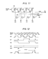
- Fig. 16 is a diagram showing the structure of a ghost canceller using a circuit using no time multiplex corresponding to the fourth embodiment of the present invention.
- Fig. 17 is a circuit diagram showing a digital signal processor according to the prior art; and
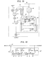
- Fig. 18 is a circuit diagram showing an example of the digital signal processor according to the present invention, in which an A/D converter and a D/A converter are integrated together on a common single chip.
- The
Embodiment 1 of the present invention will be described in the following with reference to Figs. 1, 2, 3 and 4. - In the video signal processor of the prior art shown in Fig. 2, the lefthand signal processing block 1' uses nine ALUS 4 whereas the righthand signal processing block 2' uses seven
ALUs 4 and fourmultipliers 5. In other words, the numbers of theALUs 4, i.e., the numbers of additions and subtractions of the prior art are NA1 = 9 and NA2 = 7, respectively, and the numbers of themultipliers 5, i.e., the numbers of multiplications areN M1 = 0 and NM2 = 4, respectively. - As has been described hereinbefore, on the other hand, the sampling time in the signal processing circuit (SPC) of the digital TV set is T = 70 ns, which is common between the two SPCs. The processing times of each
ALU 4 in each SPC are τA1 = TA2 = 10 ns. In the present embodiment, the processing time of eachmultiplier 5 existing only in theSPC 2 is τM2 = 12 ns. - Here, each SPC is constructed in conformity to the above-specified requirements.
- At first, from τi = max (τAi, τMi):
- τ1 = 10 ns; and
- T2 = 12 ns.
- From T/τi ≧ Pi, the numbers of the individual program steps:
- p1 = 7, 6, 5, - - -; and
- P2 = 5, 4, 3, - - -.
- From NAi ≦ Pi·MAi and NMi ≦ Pi·MMi, the numbers of the ALUs and multipliers are:
- MA1 = 2, 3, - - - , and MM1 = 0; and
- MA2 = 2, 3, - - - , and MM2 = 1, 2, - -
- As a result, the
SPC 1 can be constructed of two ALUs at the least, and theSPC 2 can be constructed of two ALUs and one multiplier at the least. - The structures of the
SPC 1 andSPC 2, which are constructed by combining the above-specified numbers of the ALUs and the multiplier with registers, latches, delay memories and coefficient memories, are shown in Fig. 1. TheseSPC 1 andSPC 2 operate in accordance with the programs shown in Figs. 3 and 4, respectively. - In Fig. 1:
reference numeral 3 designates registers; numeral 4 ALUs; numeral 5 a multiplier; numeral 6 delay memories; numeral 7 a coefficient memory; numeral 8 latches; and numeral 9 data buses. - First of all, a motion detection circuit to be realized by the
SPC 1 will be described in connection with instruction executions with reference to Figs. 1 and 3. - As shown in Fig. 3, the program step in the
SPC 1 is P1 = 5. The internal clock for advancing this program is generated by the PLL from the sampling time T = 70 ns common between the two SPCs and has a period of T/5 = 14 ns. - At a first step, input signals IN1 to IN8 are latched in registers Rl to R8.
- At a second step, the contents of the registers R1 to R4 are latched in latches Ll to L4.
- At a third step, the arithmetic results (Ll + L2)/2 and (L3 + L4)/2 of the ALU4 are latched in the latches Ll and L3, and L2 and L4, respectively.
- Thus, the program advances to the seventh step so that the process performed is equivalent to that of the circuit in Fig. 2.
- Next, the transversal filter to be realized by the
SPC 2 will be described in the following,in connection with its instruction executions with reference to Figs. 1 and 4. - At a first step, as shown in Fig. 4, input data are fed in a latch L6 (i.e., L6 = IN). Simultaneously with this, a first coefficient Cl is latched in a latch L5 (i.e., L5 = Cl) from the
coefficient memory 7. Master/ slave latches are used here so that the data are latched in response to the first-phase clock φ1 and appear in response to a second-phase clock φ2. As a result, the data are fed to themultiplier 5 at the instant when clock rises at the latter half of the first program step. - At the second step, the multiplied result is latched in two latches L8 and L10 (i.e., L8 = L6 * L5, L10*L5). Simultaneously, data to be added thereto are latched in latches L7 and L9 (i.e., L7 = Z7, L9 = 0) from the
delay memories 6, respectively. Moreover, a coefficient C2 to be subsequently multiplied is latched in the latch L5. - At the third step, the subsequent multiplied result is latched in the latches L8 and L10. Simultaneously, the added result of the latches L7 and L8 by the
arithmetic logic unit 4 is latched in the register R13 (i.e., R13 = L7 + L8), and the added result of the latches L9 and L10 is latched in a memory Zl (i.e., Zl = L9 + L10). Thus, a pipe-line process for executing the multiplication of the present data simultaneously with the addition of the preceding data is used. Moreover, the twoadders 4 operate in parallel. - In these ways, the program advances to the sixth step of Fig. 4 so that the process is similar to that of the circuit of Fig. 2. Now, because the parallel process is possible, the proceding and succeeding steps can be added to the first and sixth steps so that the sampling interval (e.g., five steps in Fig. 4) can be shortened. Incidentally, Instruction NOP appearing in Fig. 4 designate "No Operation", in which no operation is executed and which is inserted for the synchronization (i.e., five steps / sampling time) with the
SPC 1. As a result, the program advances like theSPC 1 in response to the internal clock of 14 ns. In case theSPC 1 andSPC 2 are operated in response to internal clocks which are independent of each other, the NOP can be eliminated to reduce the step number up to a rate of four steps / sampling time. - The internal clock is generated by the PLL in each SPC,synchronized with the common sampling clock in the video system. Therefore, the internal clock may be common or independent for the individual SPCs.
- The description thus far made is a general one of the video signal processor using the SPCs according to the present invention. In the present embodiment, the
SPC 1 andSPC 2 have the following features because of the motion detections executed in the SPCs and the circuit structure intrinsic to the transversal filter. - First of all, the linear phase transversal filter uses the two
adders 4 to operate in parallel. This takes it into consideration that after the inputs are multiplied with appropriate filter coefficients by themultiplier 5 its result are used in two additions simultaneously, as shown in Fig. 2. As in this case, the signal processing parallelism can be enhanced to increase the signal processing rate by making an SPC architecture according to the signal processing content. - The
SPC 1 of Fig. 1 also adopts the architecture considering the signal processing content. In thisSPC 1, the fourbus lines 9 are provided to enhance the parallelism of the data flow. - Inorder to realize the time-multiplexing process in a high-frequency range as in the video band, it is necessary to progress the progressings as many as possible simultaneously at one program step. For this requirement, the following techniques are used in the present embodiment:
- (1) The control uses a horizontal micro-program requiring no decoding.
- (2) The high speed is realized by the pipe-line processings. For example, the
SPC 2 has a three-stage pile-line including the latching, multiplication and addition. Therefore, eachlatch 8 uses the aforementioned master/slave latch. - (3) The
delay memory 6 uses a multi-port memory partly because the data are written at one step in different addresses, as at thestep 6 of Fig. 4, and partly because other words are read out, as at thesteps - With reference to Fig. 5, a
program memory 10 will be described in the following. Fig. 5 shows the circuit structure of theprogram memory 10. In Fig. 5:reference numeral 11 designate an address decoder; numeral 12 buffers; numeral 13 "1" level memory cells; numeral 14 "0" level memory cells; numeral 15 word lines; and numeral 16 data lines. On the other hand: reference letters L5E to L10E designate enable signals to be fed to the latches L5 to L10 of Fig. 1, respectively; letters CAD the address of thecoefficient memory 7; letters ZAAD the addresses of delay memories Zl, Z2 and Z3; letters ZAWE a write enable signal of these dalay memories; letters ZBAD1, ZBAD2 and ZBAD3 the addresses of delay memories Z4, Z5, Z6 and Z7; letters R13E an enable signal of the output latches; and ZBWE1 and ZBWE2 wrote enable signals of the delay memories Z4, Z5, Z6 and Z7. The stored contents correspond to the object code program of Fig. 4. For a high-speed control, each of thememory cells data line 16 connected directly with a power source Vddor grounded to the earth in accordance with its stored content. Depending on the processing speed requirements and devices, there are other options for these such as static RAMs, fusible PROMs, electrically writable EPROMs or electrically erasable EEPROMs. - A circuit for generating the addresses of the aforementioned program memories is shown in Fig. 6, and its pulse timings are shown in Fig. 7. When the internal clocks φ1 and φ2 have frequencies of 50 MHz or higher, their feeds from the outside become difficult. As shown in Fig. 6, therefore, the internal clocks are generated by a PLL circuit (i.e., Phase Locked Loop). A voltage controlled
oscillator 19 generates two-phase clocks φ1 and 02, which are counted down by abinary counter 20 which is reset for every 5 counts in accordance with the fifth program step. Here, 3-bit program memory addresses (a0, al and a2) are generated. An accurate synchronization is taken by comparing the phases of the counted-down result a2 and the sampling clock CLKS of the input signal by means of aphase comparator 17. In order to set the initial state, theaforementioned counter 20 is equipped with a reset terminal or a present terminal and a data input terminal. In Fig. 6,reference numeral 18 designates a low-pass filter. The circuit under consideration is provided either independently in each SPC or commonly for a plurality of SPCs. In either case, the value of the n-notated counter in the PLL circuit can be independently set so that the optimum instruction execution time for each SPC can be set. - Moreover, the clocks φ1 and Ø2 can be fed from the outside if no problem arises in the speed.
- In case a number of SPCs are used, it is necessary to set each operation mode and each coefficient and perform the testing reliably and promptly. This necessity can be satisfied by using SPC buses shown in Figs. 8 and 9.
- Fig. 8 shows the structure of the
SPC 2 of Fig. 1 in case the interface with the SPC buses is taken into consideration. First, the device address (DA) from theexternal SPC bus 26 is decoded by adevice decoder 23 of the SPC. If the derive address coincide with the address designated to that SPC, DS (Device Select) signal is issued. Then, the program counter is switched by amultiplexer 24 from a main-program counter 21 to asub program counter 22 which is controlled by an external clock and a preset signal. The program for setting the coefficient of theprogram memory 10, the operation mode or the testing program is controlled by this sub program counter. In the coefficient setting mode, the data (DT) from theSPC bus 26 are fed through aninternal bus 25 to thecoefficient memory 7. In the testing mode, input data are first set through theinternal bus 25 in thecoefficient memory 7, the input latch L6 and thedelay memories 6 in order to execute the filtering program of theprogram memory 10. After this, the processed results stored in the aforementioned individual memories are read out to theSPC bus 26 through theinternal bus 25.Reference numeral 27 designates a tri-state gate to be controlled by the individual control signals. - The system VLSI is arranged with a number of SPCs 28 (i.e.,
SPC 1 to SPC 5), as shown in Fig. 9. All of these SPCs are controlled either from the outside via theSPC bus 26 through an interface circuit 29 or by an internal processor 30. In Fig. 9, numeral 32 designates an external processor, and numeral 33 designates an external bus. In the ordinary operation, the signals are processed along a high-speed signal path 31 indicated by hatched arrow. In the testing or coefficient and operation mode settings, the interface circuit 29 or the internal processor 30 accesses a specific SPC to carry out those operations. In . an adaptive filter, for example, the SPC performs the filtering operation at a high speed, and the internal processor performs complicated adaptation calculations. The coefficients thus calculated are transmitted during a blanking period in the TV scanning to the SPC filter via the aforementioned SPC bus. - In this embodiment, the transversal filter in the
Embodiment 1 is enhanced, so that setting of the time multiplex degree becomes capable, and filters can be connected in cascade to have variable orders. In order to realize these features this embodiment is equipped with a circuit for setting the number of frequency divisions of a counter in the phase locked loop circuit (PLL) an input signal delay circuit, a circuit to fed external data directly to an ALU, and a circuit for outputting the data to the outside directly from the ALU. The description will proceed with reference to Fig. 10. - The transversal filter of the
Embodiment 1 of Fig. 1 is constructed of one SPC 2(2). The transversal filter of the present embodiment is constructed of two SPCs, i.e.,SPC 2A(2A) andSPC 2B(2B) which are connected in cascade. A multiplex number N sets the number of frequency divisions of afrequency dividing counter 38 by amultiplex number register 37 and partially changes the content of theprogram memory 10. Since, moreover, the signal from the preceding stage can be transferred to the register L7 of theALU 4 by aninput switching circuit 35, the SPCs can be connected in cascade. This enables the filter to extend its order to an arbitrary value. Moreover, theprogram memory 10 and thefrequency dividing counter 38 can be set in accordance with the content of themultiplex number register 37 so that the multiplex degree can be set in conformity to the speed required of the system to which the present invention is applied. An inputsignal delay circuit 34 is provided to ensure a synchronization between the two delays of the output register R13 and the register L7 of the ALU and an input signal even if the two delays come from the cascade connection. Incidentally, Fig. 10 shows the SPC as includes not only the portion indicated atSPC 2 in Fig. 1 but also the program memory shown in Fig. 5 and the PLL portion shown in Fig. 6. - Next, the features of the present embodiment will be described in detail.
- The setting of the time multiplex number can be changed by setting the number of frequency divisions of the
frequency dividing counter 38 in aPLL circuit 36 by means of a circuit shown in Fig. 11. The timing charts are shown in Fig. 12. A T flip-flop 39 alter the output Q in response to the fall of the input signal T. The output Q is reset by inputting a '0' signal to the reset terminal R. An exclusive OR circuit outputs thelogical level 0, when each binary output Q1 of the T flip-flop and a time multiplex number Ni coincide, and resets each T flip-flop 39 through anOR gate 40 at its output terminal only when all the bits coincide. This behavior is shown in Fig. 12. Here, the multiplex degree is set at N = 6 or (N0. N1, N2 and N3) = (0 1 1 0) in the binary notation. In the reset signal RST, there appear pulses from the voltage controlled oscillator VCO, which are compared for synchronization with the external CL. The present signal processor can be used six times time-multiplexly by using the output of the VCO as the control clocks. As a result, the number of frequency divisions of the counter and the time multiplex degree can be changed by setting the value of the time multiplex degree N. - The circuit shown in Fig. 10 can be operated like the filter shown in Fig. 14 if it follows the programs shown in Figs. 13A and 13B. Two directions of signal flow are present in Fig. 14. One is a rightward signal flow of L7 - Zl - Z3 - R13 and the other is a leftward signal flow of L10 - Z4 - Z2 - Z13. This is because the individual filter coefficients of the signals to be sequentially added are set at Cl, C2, C3, - - -, and C3, C2, Cl by folding back the rightward signals leftward after they have passed through a predetermined number of steps of filters. By making the orders of the individuals coefficients thus symmetric, an equal group delay can be given to the input signals of all frequencies.
- This embodiment is modified from the transversal filter of the
Embodiment 4 such that not only the tap coefficients but also the delay between each filter tap can be set. This filter circuit is appropriate for a ghost canceller circuit of a TV receiver or the like. - Fig. 15 shows the structure of the SPC of the filter portion of the present embodiment. Each
variable delay circuit 41 is constructed of: ashift register 42 for operating in synchronism with a sampling clock; amultiplexer 43 for selecting the outputs of the shift register; and a delay number register 44 for latching the delay number. The amount of delay of each delay circuit is set like the filter tap coefficient through adata bus 45. The filter tap coefficient is latched in thecoefficient memory 7. Moreover:letter 8 designates registers; numeral 46 an internal data bus; numeral 47 a delay circuit output multiplexer; numeral 48 an extension circuit input multiplexer; and numeral 49 an interface circuit (I/O). Thecoefficient memory 7 latches the filter tap coefficients for five taps. The present embodiment is featured by the fact that thevariable delay circuits 41 are used d3 registers for latching delay data. - According to the filter circuit using the SPC of this embodiment as shown in Fig. 15, a filter circuit shown in Fig. 16 can be realized with a small number of elements. The filter circuit of Fig. 16 is a ghost canceller for eliminating the ghost from by substracting the ghost signal synthesized by the filter from a ghost containing signal coming from the input terminal.
- The number of elements in the digital signal processor is reduced by the process of present invention so that an analog/digital (A/D) converter, a digital/analog (i.e., D/A) converter and so on can be integrated on a common single chip.
- Fig. 17 shows a circuit example of the digital signal processor of the prior art not using the process of the present invention, as has been reported on pp. 152 and 153, ISSCC "Digest of Technical Papers", 1986. This circuit separates an illuminance signal Y and a chrominance signal C from the NTSC composite video signal of a television system. The oeprations of this circuit will be described briefly in the following.
- An analog NTSC signal is converted into a 8-bit digital signal by an A/
D converter 102 and is inputted to adigital signal processor 101. This digital signal is delayed a predetermined amount byline memories 108 and adelay memory 109 until it is fed as signals Sl to S9 to asignal difference estimator 115 or adifferential estimator 116.Reference numerals signal difference estimator 115 anddifferential estimator 116 becomes the control signal for the adaptive Y/C separation and fed to multiplexers 112. According to these control signals, the NTSC composite signal is separated adaptively into 8-bit digital illuminance and chrominance signals, and are outputted from thedigital signal processor 101 so that they are converted into analog illuminance and chrominance signals Y and C. - If this digital signal processor is designed by the technology based on the present invention, the number of circuit elements of the digital signal processor can be drastically reduced so that the A/D converter and the D/A converter can be integrated on the chip shared with the digital signal processor by making use of the reduced space on the chip, as shown in Fig. 18.
- In Fig. 18, reference numerals 104-1, 104-2 and 104-3 designate the individual portions of the digital signal processor, in which the number of elements is reduced by the process of the present invention.
Numerals D converter 102 and the D/A converter 103 are integrated on the chip shared with the digital signal processor by making use of the space which is established by reducing the element number. The number of signal input pin is only one for the analog NTSC and only two for the analog Y and C, so that the number of pins, and consequently the price of the package can be reduced drastically.
Claims (4)
Applications Claiming Priority (6)
| Application Number | Priority Date | Filing Date | Title |
|---|---|---|---|
| JP142998/86 | 1986-06-20 | ||
| JP61142998A JPH0828834B2 (en) | 1986-06-20 | 1986-06-20 | Signal processor |
| JP16184386A JPS6318812A (en) | 1986-07-11 | 1986-07-11 | Semiconductor integrated circuit device |
| JP161843/86 | 1986-07-11 | ||
| JP61190519A JPS6348079A (en) | 1986-08-15 | 1986-08-15 | Semiconductor integrated circuit device |
| JP190519/86 | 1986-08-15 |
Publications (3)
| Publication Number | Publication Date |
|---|---|
| EP0249962A2 true EP0249962A2 (en) | 1987-12-23 |
| EP0249962A3 EP0249962A3 (en) | 1990-03-21 |
| EP0249962B1 EP0249962B1 (en) | 1994-05-04 |
Family
ID=27318550
Family Applications (1)
| Application Number | Title | Priority Date | Filing Date |
|---|---|---|---|
| EP87108699A Expired - Lifetime EP0249962B1 (en) | 1986-06-20 | 1987-06-16 | Digital video signal processor |
Country Status (3)
| Country | Link |
|---|---|
| US (1) | US4825287A (en) |
| EP (1) | EP0249962B1 (en) |
| DE (1) | DE3789731T2 (en) |
Cited By (6)
| Publication number | Priority date | Publication date | Assignee | Title |
|---|---|---|---|---|
| FR2652973A1 (en) * | 1989-10-06 | 1991-04-12 | Europ Rech Electr Lab | INTERPOLATOR FOR TELEVISEUR AND TELEVISEUR COMPRISING SUCH INTERPOLATEUR. |
| GB2240684A (en) * | 1990-02-06 | 1991-08-07 | Sony Corp | Cascaded digital signal interpolator |
| EP0449075A2 (en) * | 1990-03-30 | 1991-10-02 | Kabushiki Kaisha Toshiba | Image reproduction apparatus |
| US5285264A (en) * | 1990-03-30 | 1994-02-08 | Kabushiki Kaisha Toshiba | Image reproduction apparatus with plural program processing |
| CN1047051C (en) * | 1994-10-28 | 1999-12-01 | Lg电子株式会社 | Communication control device and method for TV receiver |
| US11256327B2 (en) | 2018-06-13 | 2022-02-22 | Tobii Ab | Eye tracking device and method for manufacturng an eye tracking device |
Families Citing this family (16)
| Publication number | Priority date | Publication date | Assignee | Title |
|---|---|---|---|---|
| US5379351A (en) * | 1992-02-19 | 1995-01-03 | Integrated Information Technology, Inc. | Video compression/decompression processing and processors |
| US6751696B2 (en) * | 1990-04-18 | 2004-06-15 | Rambus Inc. | Memory device having a programmable register |
| IL96808A (en) | 1990-04-18 | 1996-03-31 | Rambus Inc | Integrated circuit i/o using a high performance bus interface |
| US6324120B2 (en) | 1990-04-18 | 2001-11-27 | Rambus Inc. | Memory device having a variable data output length |
| US6965644B2 (en) * | 1992-02-19 | 2005-11-15 | 8×8, Inc. | Programmable architecture and methods for motion estimation |
| US5594813A (en) * | 1992-02-19 | 1997-01-14 | Integrated Information Technology, Inc. | Programmable architecture and methods for motion estimation |
| WO1994020927A1 (en) * | 1993-03-12 | 1994-09-15 | Integrated Information Technology, Inc. | Programmable architecture and methods for motion estimation |
| EP0710033A3 (en) * | 1994-10-28 | 1999-06-09 | Matsushita Electric Industrial Co., Ltd. | MPEG video decoder having a high bandwidth memory |
| US5623311A (en) * | 1994-10-28 | 1997-04-22 | Matsushita Electric Corporation Of America | MPEG video decoder having a high bandwidth memory |
| US5920352A (en) * | 1994-10-28 | 1999-07-06 | Matsushita Electric Industrial Co., Ltd. | Image memory storage system and method for a block oriented image processing system |
| US6085309A (en) * | 1997-01-08 | 2000-07-04 | Yamaha Corporation | Signal processing apparatus |
| EP1122637A3 (en) * | 2000-01-31 | 2005-10-12 | Micronas GmbH | Computation unit for limited signal processing |
| DE10009451C1 (en) * | 2000-01-31 | 2001-05-03 | Micronas Gmbh | Signal processing device e.g. for digital video signal processing has position shifting devices controlled by shifting instruction dependent on one coded number supplied with second coded number at their setting inputs |
| KR100377176B1 (en) * | 2000-06-12 | 2003-03-26 | 주식회사 하이닉스반도체 | Encryption device using data encryption standard algorithm |
| US8526486B2 (en) * | 2008-11-12 | 2013-09-03 | Intel Corporation | Decision feedback equalizer for portable environments |
| US8504961B2 (en) * | 2010-06-01 | 2013-08-06 | Arm Limited | Integrated circuit with timing adjustment mechanism |
-
1987
- 1987-06-16 DE DE3789731T patent/DE3789731T2/en not_active Expired - Fee Related
- 1987-06-16 EP EP87108699A patent/EP0249962B1/en not_active Expired - Lifetime
- 1987-06-18 US US07/063,476 patent/US4825287A/en not_active Expired - Fee Related
Non-Patent Citations (4)
| Title |
|---|
| Computer Architectures and Parallel Processing, Hwang and Briggs, International Edition, 1985, McGraw-Hill Book Co., Singapore, pages 145 to 151 * |
| IEEE INTERNATIONAL SOLID STATE CIRCUITS CONFERENCE, 20th February 1983, pages 258-259, IEEE, New York, US; T. MORI et al.: "A micro-programmable realtime image processor" * |
| IEEE INTERNATIONAL SOLID STATE CIRCUITS CONFERENCE, 20th February 1986, pages 152-153, IEEE, New York, US; M. YOSHIMOTO et al.: "A digital processor for decoding of composite TV signals using adaptive filtering" * |
| IEEE INTERNATIONAL SOLID STATE CIRCUITS CONFERENCE, 25th February 1983, pages 258-259, IEEE, New York, US; T. FUKUSHIMA et al.: "An image-signal processor" * |
Cited By (9)
| Publication number | Priority date | Publication date | Assignee | Title |
|---|---|---|---|---|
| FR2652973A1 (en) * | 1989-10-06 | 1991-04-12 | Europ Rech Electr Lab | INTERPOLATOR FOR TELEVISEUR AND TELEVISEUR COMPRISING SUCH INTERPOLATEUR. |
| EP0427576A1 (en) * | 1989-10-06 | 1991-05-15 | Laboratoire Europeen De Recherches Electroniques Avancees | Interpolator for a sub-sampling transmission system |
| GB2240684A (en) * | 1990-02-06 | 1991-08-07 | Sony Corp | Cascaded digital signal interpolator |
| GB2240684B (en) * | 1990-02-06 | 1994-02-23 | Sony Corp | Digital signal interpolation |
| EP0449075A2 (en) * | 1990-03-30 | 1991-10-02 | Kabushiki Kaisha Toshiba | Image reproduction apparatus |
| EP0449075A3 (en) * | 1990-03-30 | 1992-05-20 | Kabushiki Kaisha Toshiba | Image reproduction apparatus |
| US5285264A (en) * | 1990-03-30 | 1994-02-08 | Kabushiki Kaisha Toshiba | Image reproduction apparatus with plural program processing |
| CN1047051C (en) * | 1994-10-28 | 1999-12-01 | Lg电子株式会社 | Communication control device and method for TV receiver |
| US11256327B2 (en) | 2018-06-13 | 2022-02-22 | Tobii Ab | Eye tracking device and method for manufacturng an eye tracking device |
Also Published As
| Publication number | Publication date |
|---|---|
| EP0249962A3 (en) | 1990-03-21 |
| DE3789731T2 (en) | 1994-08-18 |
| EP0249962B1 (en) | 1994-05-04 |
| DE3789731D1 (en) | 1994-06-09 |
| US4825287A (en) | 1989-04-25 |
Similar Documents
| Publication | Publication Date | Title |
|---|---|---|
| US4825287A (en) | Digital video signal processor | |
| US5327125A (en) | Apparatus for and method of converting a sampling frequency according to a data driven type processing | |
| US3979701A (en) | Non-recursive digital filter employing simple coefficients | |
| EP0287331B1 (en) | Sampled data memory system eg for a television picture magnification system | |
| AU2400799A (en) | A method for addressing memory | |
| US4644488A (en) | Pipeline active filter utilizing a booth type multiplier | |
| US4464675A (en) | Low frequency digital comb filter system | |
| EP0100678B1 (en) | Reduced data rate signal separation system | |
| US5793443A (en) | Motion vector detection circuit | |
| US5663767A (en) | Clock re-timing apparatus with cascaded delay stages | |
| EP0435951B1 (en) | Video signal processing and video stores | |
| US4694413A (en) | Compact-structure input-weighted multitap digital filters | |
| US4814875A (en) | Digital envelope shaping apparatus | |
| US5838387A (en) | Digital video scaling engine | |
| KR960004127B1 (en) | Transversal filter | |
| US5349547A (en) | Bidimensional FIR filter | |
| Joanblanq et al. | A 54-MHz CMOS programmable video signal processor for HDTV applications | |
| KR940001556B1 (en) | Digital signal processing apparatus | |
| EP0201128B1 (en) | Integrated electronic multiplex circuit and integrated electronic circuit including such a multiplex circuit | |
| Yamazaki et al. | A 1-GOPS CMOS programmable video signal processor | |
| JPS6248888A (en) | Frequency reducer for digital sample | |
| US4041297A (en) | Real-time multiplier with selectable number of product digits | |
| KR0119392Y1 (en) | Vertical interpolation device of hdtv decoder | |
| Ulbrich et al. | MOS-VLSI pipelined digital filters for video applications | |
| Enami et al. | Real-time video signal processor |
Legal Events
| Date | Code | Title | Description |
|---|---|---|---|
| PUAI | Public reference made under article 153(3) epc to a published international application that has entered the european phase |
Free format text: ORIGINAL CODE: 0009012 |
|
| AK | Designated contracting states |
Kind code of ref document: A2 Designated state(s): DE FR GB |
|
| PUAL | Search report despatched |
Free format text: ORIGINAL CODE: 0009013 |
|
| AK | Designated contracting states |
Kind code of ref document: A3 Designated state(s): DE FR GB |
|
| 17P | Request for examination filed |
Effective date: 19900829 |
|
| 17Q | First examination report despatched |
Effective date: 19920626 |
|
| GRAA | (expected) grant |
Free format text: ORIGINAL CODE: 0009210 |
|
| AK | Designated contracting states |
Kind code of ref document: B1 Designated state(s): DE FR GB |
|
| REF | Corresponds to: |
Ref document number: 3789731 Country of ref document: DE Date of ref document: 19940609 |
|
| ET | Fr: translation filed | ||
| PLBE | No opposition filed within time limit |
Free format text: ORIGINAL CODE: 0009261 |
|
| STAA | Information on the status of an ep patent application or granted ep patent |
Free format text: STATUS: NO OPPOSITION FILED WITHIN TIME LIMIT |
|
| 26N | No opposition filed | ||
| PGFP | Annual fee paid to national office [announced via postgrant information from national office to epo] |
Ref country code: DE Payment date: 19950828 Year of fee payment: 9 |
|
| PG25 | Lapsed in a contracting state [announced via postgrant information from national office to epo] |
Ref country code: DE Effective date: 19970301 |
|
| PGFP | Annual fee paid to national office [announced via postgrant information from national office to epo] |
Ref country code: GB Payment date: 19980605 Year of fee payment: 12 |
|
| PGFP | Annual fee paid to national office [announced via postgrant information from national office to epo] |
Ref country code: FR Payment date: 19980616 Year of fee payment: 12 |
|
| PG25 | Lapsed in a contracting state [announced via postgrant information from national office to epo] |
Ref country code: GB Free format text: LAPSE BECAUSE OF NON-PAYMENT OF DUE FEES Effective date: 19990616 |
|
| PG25 | Lapsed in a contracting state [announced via postgrant information from national office to epo] |
Ref country code: FR Free format text: THE PATENT HAS BEEN ANNULLED BY A DECISION OF A NATIONAL AUTHORITY Effective date: 19990630 |
|
| GBPC | Gb: european patent ceased through non-payment of renewal fee |
Effective date: 19990616 |
|
| REG | Reference to a national code |
Ref country code: FR Ref legal event code: ST |