EP0256864A2 - Digital data processing apparatus - Google Patents
Digital data processing apparatus Download PDFInfo
- Publication number
- EP0256864A2 EP0256864A2 EP87307179A EP87307179A EP0256864A2 EP 0256864 A2 EP0256864 A2 EP 0256864A2 EP 87307179 A EP87307179 A EP 87307179A EP 87307179 A EP87307179 A EP 87307179A EP 0256864 A2 EP0256864 A2 EP 0256864A2
- Authority
- EP
- European Patent Office
- Prior art keywords
- memory
- bus
- unit
- cycle
- transfer
- Prior art date
- Legal status (The legal status is an assumption and is not a legal conclusion. Google has not performed a legal analysis and makes no representation as to the accuracy of the status listed.)
- Granted
Links
Images


Classifications
-
- G—PHYSICS
- G06—COMPUTING; CALCULATING OR COUNTING
- G06F—ELECTRIC DIGITAL DATA PROCESSING
- G06F11/00—Error detection; Error correction; Monitoring
- G06F11/07—Responding to the occurrence of a fault, e.g. fault tolerance
- G06F11/16—Error detection or correction of the data by redundancy in hardware
- G06F11/20—Error detection or correction of the data by redundancy in hardware using active fault-masking, e.g. by switching out faulty elements or by switching in spare elements
- G06F11/202—Error detection or correction of the data by redundancy in hardware using active fault-masking, e.g. by switching out faulty elements or by switching in spare elements where processing functionality is redundant
- G06F11/2043—Error detection or correction of the data by redundancy in hardware using active fault-masking, e.g. by switching out faulty elements or by switching in spare elements where processing functionality is redundant where the redundant components share a common memory address space
-
- G—PHYSICS
- G06—COMPUTING; CALCULATING OR COUNTING
- G06F—ELECTRIC DIGITAL DATA PROCESSING
- G06F11/00—Error detection; Error correction; Monitoring
- G06F11/07—Responding to the occurrence of a fault, e.g. fault tolerance
- G06F11/16—Error detection or correction of the data by redundancy in hardware
- G06F11/1608—Error detection by comparing the output signals of redundant hardware
- G06F11/1616—Error detection by comparing the output signals of redundant hardware where the redundant component is an I/O device or an adapter therefor
-
- G—PHYSICS
- G06—COMPUTING; CALCULATING OR COUNTING
- G06F—ELECTRIC DIGITAL DATA PROCESSING
- G06F11/00—Error detection; Error correction; Monitoring
- G06F11/07—Responding to the occurrence of a fault, e.g. fault tolerance
- G06F11/16—Error detection or correction of the data by redundancy in hardware
- G06F11/1629—Error detection by comparing the output of redundant processing systems
- G06F11/1641—Error detection by comparing the output of redundant processing systems where the comparison is not performed by the redundant processing components
-
- G—PHYSICS
- G06—COMPUTING; CALCULATING OR COUNTING
- G06F—ELECTRIC DIGITAL DATA PROCESSING
- G06F11/00—Error detection; Error correction; Monitoring
- G06F11/07—Responding to the occurrence of a fault, e.g. fault tolerance
- G06F11/16—Error detection or correction of the data by redundancy in hardware
- G06F11/1666—Error detection or correction of the data by redundancy in hardware where the redundant component is memory or memory area
- G06F11/167—Error detection by comparing the memory output
-
- G—PHYSICS
- G06—COMPUTING; CALCULATING OR COUNTING
- G06F—ELECTRIC DIGITAL DATA PROCESSING
- G06F11/00—Error detection; Error correction; Monitoring
- G06F11/22—Detection or location of defective computer hardware by testing during standby operation or during idle time, e.g. start-up testing
-
- G—PHYSICS
- G11—INFORMATION STORAGE
- G11C—STATIC STORES
- G11C29/00—Checking stores for correct operation ; Subsequent repair; Testing stores during standby or offline operation
- G11C29/70—Masking faults in memories by using spares or by reconfiguring
- G11C29/74—Masking faults in memories by using spares or by reconfiguring using duplex memories, i.e. using dual copies
-
- G—PHYSICS
- G06—COMPUTING; CALCULATING OR COUNTING
- G06F—ELECTRIC DIGITAL DATA PROCESSING
- G06F11/00—Error detection; Error correction; Monitoring
- G06F11/07—Responding to the occurrence of a fault, e.g. fault tolerance
- G06F11/08—Error detection or correction by redundancy in data representation, e.g. by using checking codes
- G06F11/10—Adding special bits or symbols to the coded information, e.g. parity check, casting out 9's or 11's
-
- G—PHYSICS
- G06—COMPUTING; CALCULATING OR COUNTING
- G06F—ELECTRIC DIGITAL DATA PROCESSING
- G06F11/00—Error detection; Error correction; Monitoring
- G06F11/07—Responding to the occurrence of a fault, e.g. fault tolerance
- G06F11/14—Error detection or correction of the data by redundancy in operation
-
- G—PHYSICS
- G06—COMPUTING; CALCULATING OR COUNTING
- G06F—ELECTRIC DIGITAL DATA PROCESSING
- G06F11/00—Error detection; Error correction; Monitoring
- G06F11/07—Responding to the occurrence of a fault, e.g. fault tolerance
- G06F11/16—Error detection or correction of the data by redundancy in hardware
- G06F11/20—Error detection or correction of the data by redundancy in hardware using active fault-masking, e.g. by switching out faulty elements or by switching in spare elements
- G06F11/202—Error detection or correction of the data by redundancy in hardware using active fault-masking, e.g. by switching out faulty elements or by switching in spare elements where processing functionality is redundant
- G06F11/2023—Failover techniques
- G06F11/2028—Failover techniques eliminating a faulty processor or activating a spare
Landscapes
- Engineering & Computer Science (AREA)
- Theoretical Computer Science (AREA)
- General Engineering & Computer Science (AREA)
- Quality & Reliability (AREA)
- Physics & Mathematics (AREA)
- General Physics & Mathematics (AREA)
- Computer Hardware Design (AREA)
- Communication Control (AREA)
- Debugging And Monitoring (AREA)
- Bus Control (AREA)
- Techniques For Improving Reliability Of Storages (AREA)
- Test And Diagnosis Of Digital Computers (AREA)
Abstract
Description
- The invention relates to digital data processing apparatus and, more particularly, to memory units for fault-tolerant computers.
- Faults in digital computer systems are inevitable and are due, at least in part, to the complexity of the circuits, the associated d electromechanical devices, and the process control software. To permit system operation even after the occurrence of a fault, the art has developed a number of fault-tolerant designs. Among these is Rennels, "Architecture for Fault-Tolerant Spacecraft Computers", proceedings of the I.E.E.E., Vol. 66, No. 10, pp. 1255-1268 (1975), disclosing a computer system comprised of independent self-checking modules. In the event of failure of a sub-component of one of the modules, the entire SCCM is taken off-line for diagnostic testing.
- An improved fault-tolerant digital data processing system is currently available from the present applicants, Stratus Computer Company, of Marlboro, Massachusetts. This system employs redundant functional unit pairs, e.g., dual redundant memory units, providing continuous processing in the event one unit of the pair fails. The functional units of the Stratus System are interconnected for information transfer on a common bus structure. The transfers are pipelined; that is, each unit-to-unit transfer occurs during plural phases and overlaps the phases of other unit-to-unit transfers.
- The currently available Stratus system includes, in one embodiment, dual redundant memory units. In the event one of these units becomes faulty, an update feature facilitates copying information from the original non-faulty partner to a replacement memory unit. This update feature operates under the control of the system's central processing unit, which reads information on a word-by-word basis from the original, non-faulty unit and writes that information to the new unit. Memory transfers carried out in this manner must arbitrate for the bus with all other system tasks and, thus, on a busy system, can take substantial time to complete.
- With respect to timing functions, the art provides numerous computer systems in which time-of-day information is obtained via function calls to the operating system. Whenever such a function call is made, e.g., by a peripheral control unit, the time-of-day information will not become available until after the central processing unit is freed from other intervening tasks.
- With this background, an object of the invention is to provide an improved digital data processing system. More particularly, an object of the invention is to provide an improved memory device for a fault-tolerant computer.
- The present invention is digital data processing apparatus that utilizes a common bus structure for transferring information between a first functional unit and other functional units of the digital data processing apparatus, said first and other functional units being any of a processing unit, a peripheral control unit, and a memory unit, said first functional unit including a processing section responsive to input signals received on said bus structure from said other functional units for generating output signals for transmission on said bus structure to said other functional units, said apparatus including clock means connected with said functional units for providing signals defining successive timing intervals, said apparatus executing a unit-to-unit information transfer on the bus structure by transferring signals representative of a transfer cycle that occurs during plural timing intervals and includes plural phases, including a definition phase which can include addressing, a response phase, and a data-transfer phase, where the phases of one cycle are non-overlapping and occur in sequence in different respective timing intervals of the transfer cycle, said bus structure including means for carrying definition signals representative of data-transfer phases, said functional units being arranged for pipelining transfer cycles by transferring concurrently on the bus structure signals representative of differing phases of plural cycles, said apparatus being characterized in that A. said first functional unit comprises diagnostic means connected with said processing section for performing a diagnostic cycle thereon during at least a first timing interval common to first and second pipelined transfer cycles, said diagnostic means including means for generating a BUSY signal indicative of onset of said diagnostic cycle, and B. said apparatus comprises pipeline-interrupt means responsive to detection of said BUSY signal for aborting the further execution of said second transfer cycle while continuing the execution of said second transfer cycle.
- Embodiments of the present invention will now be described, by way of example, with reference to the accompanying drawings, in which:-
- Fig. 1 illustrates a digital data processor according to the present invention;
- Figs. 2A to 2E are signal/phase diagrams illustrating the operation of the processor of Fig. 1;
- Fig. 3 is a circuit diagram of the
main memory unit 16 of Fig. 1; - Fig. 4 is a circuit diagram of a bus error stage of Fig. 3;
- Fig. 5 is a circuit diagram of the memory format section of the
main memory unit 16; and - Fig. 6 illustrates a memory unit gate array.
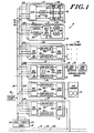
- A
digital data processor 10 according to the invention has, as FIG. 1 shows, a central processing unit (CPU) 12, amain memory unit 16, and control units for peripheral input/output devices, including, for example, adisc control unit 20, acommunication control unit 24, atape control unit 28, and alink control unit 32. A singlecommon bus structure 30 interconnects the units to provide all information transfers and other signal communications between them. Thebus structure 30 also provides operating power to the units of the module from amain supply 36 and provides system timing signals from amain clock 38. - The
bus structure 30 includes twoidentical buses X bus 46. In general, the signals on the A bus and on the B bus execute information transfers between units of themodule 10. Accordingly, these buses carry function, address, and data signals. The X bus in general carries signals that serve multiple units in the module. These include main power, timing, status and fault-responsive signals. Eachunit 12 through 28, 32 and 34 is connected to all three buses of thebus structure 30. This enables each unit to transfer signals on either or both the A bus and the B bus, as well as on the X bus. - With further reference to FIG. 1, each functional unit of the
module 10 can have a back-up redundant partner unit. Accordingly, the illustrated module has a secondcentral processing unit 14, asecond memory unit 18, a second disc.control unit 22, a secondcommunication control unit 26, and a secondlink control unit 34. - The basic operation of the
system 10 is that, in the absence of a fault, the partnered functional units, except those controlling asynchronous peripheral devices, operate in lock-step synchronism with one another. Thus, for example, bothmemory units central processing units communication control units communication control units communication bus 48 that connects to one ormore communication panels 50 which are connected to conventional communication devices such as keyboards, cathode ray tube terminals, printers and modems. - The
disc control units 20 and 22, on the other hand, do not operate in full synchronism with one another because thedisc memories disc control unit 20 and 22 writes data received from onebus memory 52 connected with it. Hence two disc memories, each connected to a different disc control unit, contain identical data. During a read operation, the system reads the stored data from one of these twomemories 52 depending on whichcontrol unit 20, 22 is available and can effect the read operation in the least time, which typically means with the shortest access time. The twolink controllers - The
units 12 through 28, 32 and 34 of the processor module of FIG. 1 check for fault conditions during each information transfer. In the event a fault is detected, the unit in question is immediately disabled from driving information onto thebus structure 30. This protects the computer system from the transfer of potentially faulty information between any units. The partner of the faulty unit, however, continues operating. The system can thus detect a fault condition and continue operating without any interruption being apparent to the user. Theprocessor module 10 provides this fault-tolerant operation by means of an improved hardware structure, rather than relying extensively on the operating system or other software control. - The
peripheral control units bus structure 30. In the event of a fault, the faulty unit is inhibited from driving information on to the bus. Operation continues, however, with the non-faulty partner unit alone driving the information onto the bus structure. - With respect to the memory and central processing units it is more timewise efficient, to proceed with information transfers without any delay for fault checking. Accordingly, the illustrated
central processing units memory units - The
processor system 10 of FIG. 1 thus operates in a manner in which a data transfer from any peripheral control units is delayed for one clock phase to provide for a fault-checking step, whereas transfers from the CPU or memory proceed without such delay and are cancelled in the event of a fault detection. In either of the foregoing instances, after completion of an information transfer during which a fault condition was detected, the potentially faulty unit remains isolated from driving information onto the A bus or the B bus, and the partner of the faulty unit continues operating. - FIG 1 shows a
main memory unit 16, having a random access memory (RAM) that is divided into twoRAM sections transceiver 16c is connected with theA bus 42 and theX bus 46 and anidentical transceiver 16d is connected with theB bus 44 and theX bus 46. Aformat section 16e of multiplex, ECC and compare circuitry in the memory unit couples either the A bus or the B bus with theRAM sections buses Partner memory unit 18 is constructed identically tounit 16. - An error checking and correcting (ECC) portion of the
memory unit section 16e provides an error checking code on every word written into theRAM sections section 16e, the memory unit raises a fault signal that is sent to all units of themodule 10. More particularly, the faulty memory unit asserts both Bus Error signals. Depending on status set in that memory unit, it either corrects the data and re-transmits it on the A and B buses, or goes off-line. The partner memory unit, if present, responds to the Bus Error signals and re-transmits the correct data. - The illustrated
memory unit 16 is configured with either 32 Mbytes, in 8 Mbyte leaves, or 8 Mbytes of random access memory organized in 2 Mbyte leaves, four-way interleaved. Each leaf is arranged for storing 72-bit words, including 64 data bits and 8 error correcting bits. Each of the illustrated RAM's 16a, 16b retain one-half of this information, i.e.,RAM 16a storesRAM 16b storesleaf # 0stores memory words stores memory words leaf # 2stores memory words leaf # 3stores memory words memory WORD 1 might be accessed by addressing location (0,0) of each of the chips in the array comprisingleaf # 1. - In addition to testing for faults within the unit, the
memory unit 16 provides fault detection for the A and B buses of themodule 10. For this purpose, the compare portion of theformat section 16e compares all signals which thememory unit 16 receives from theA bus 42 with those the unit receives from theB bus 44. When themodule 10, and particularly thebuses section 16e can note the fault. Theformat section 16e also tests the code of received signals and produces an error signal identifying any bus which has a coding error. TheX bus 46 communicates this Bus Error signal to all units of themodule 10 to instruct that each disregard the signals on that bus. - With further reference to FIG. 1, it is seen that the
central processing unit 12, identical to thepartner unit 14, has two processor sections 12a and 12b, a MAP 12c connected with the two processing sections to provide virtual memory operation, a control section 12d and transceivers 12e that transfer signals between the processing unit and thebuses unit 12. They operate essentially identically and in total synchronism with one another. Acomparator 12f compares signals output from the two processing sections and produces a fault signal if corresponding signals from the two sections differ. In response to the fault signal, the control section, among other operations, produces an error signal that theX bus 46 transmits to all units of themodule 10. The control section then isolates that unit from driving further signals onto thebus structure 30. - The error signal which the failing unit sends to other units is, in the illustrated module, a pair of signals termed an A Bus Error signal and a B Bus Error signal. Any illustrated unit in the
module 10 produces this pair of signals on the X bus when it detects certain error-producing faults. Any failing unit also produces an interrupt signal that causes the central processing unit of the module to interrogate the different units to locate the faulty one. - The
central processing unit 12 receives power from one of two identical bulk supplies 36a and 36b in themain power supply 36. Thepartner CPU 14 receives main power from the other bulk supply. Hence a failure of one bulk supply disables only one of the twopartner CPUs unit 12 has a power stage that produces supply voltages for theCPU 12. The power stage monitors the bus supply voltage from themain system supply 36, and monitors the further voltages it produces, to produce power fault signals. As noted, the hardware of theCPU 12 responds to any fault condition which is developed within the unit to, among other operations, disable the drivers of the transceivers 12e from sending potentially erroneous information from theunit 12 to the bus structured - The
disc control unit 20, identical to the partner disc control unit 22, has a bus interface section 20a, two identical disc control sections 20b and 20c, and a disc interface section 20d. The bus interface section 20a, which in the illustrated system is essentially standard for all control units, couples input signals from either theA bus 42 or theB bus 44, with a multiplexer, to the disc control sections 20b and 20c. It also applies output signals to the A bus and the B bus. However, prior to applying output signals to the buses, the bus interface section 20a compares output signals from the two control sections 20b and 20c and, in the event of an invalid comparison, disables output drivers in the interface section to prevent potentially erroneous signals from being applied to thebus structure 30. Thedisc control unit 20 receives operating power from onemain bulk supply 36a and the partner unit 22 receives operating power from theother bulk supply 36b. - Each illustrated disc control section 20b and 20c has a programmed microprocessor which provides read and write operations and associated control operations for operating the
disc memories 52. Two sections are provided to facilitate checking operations within theunit 20. The disc interface section 20d applies control and write-data signals from the unit to the disc memories, and applies status and read data signals from the disc memories to the control sections. The disc interface section 20d tests various signals for error-producing faults with parity and comparison techniques. - With continued reference to FIG. 1, the
communication control unit 24, like theidentical partner 26, has a bus interface section 24a identical in large part at least to the interface section 20a of thedisc unit 20. Thecommunication unit 24 also has twocommunication section communication interface section 24d. There is also a lock-step circuit 24e that brings theunit 24 into exact synchronism with thepartner unit 26. The bus interface section 24a functions essentially like the bus interface section 20a of the disc control unit. In the illustrated module, thecommunication control section 24b serves as a drive section to provide control, address, data and status functions for thecommunication panels 50, and the other section serves as a check section to duplicate these operations for error checking purposes. Thecommunication interface section 24b provides error checking functions similar to those described with regard to the disc interface section 20d of thedisc control unit 20. - Similarly, the
link control unit 32, which is identical to thepartner unit 34, has abus interface section 32a connected with two redundantlink control sections link interface section 32d connected between the two control section sections and the conductor set 40a of the link 40. Thepartner unit 34 connects with the other conductor set 40b. - The single
tape control unit 28 is constructed basically like the other control units with abus interface section 28a connected with all three buses, 42, 44 and 46 of thebus structure 30, with twotape control sections 28b and 28c, and with a tape interface section 28d that connects with atape transport 54. - Various digital data processor elements shown in FIG. 1, e.g., central processing and peripheral device control units, as well as bus, backplane, and power circuitry, used in a preferred practice of the invention, are commercially available from Stratus Computer Company, of Marlboro, Massachusetts. A preferred memory unit architecture and operational sequence are discussed infra.
- The
bus structure 30 which interconnects all units of the FIG. 1 processor is connected to the units by way of a backplane which has an array of connectors, to which the units connect, mounted on a panel to which the bus conductors are wired. The backplane is thus wired with duplicated conductors of theA bus 42 and theB bus 44 and with non-duplicated conductors of theX bus 46. - The illustrated system of FIG. 1 operates in one of three bus or backplane modes; namely, obey both the A bus and the B bus, obey the A bus, or obey the B bus. In all three modes, the A bus and the B bus are driven with identical signals in lock-step synchronization, but units actuated to receive data ignore the other bus in the Obey A mode and in the Obey B mode. In all modes, parity is continually generated, and checked, and any unit may signal that either bus is potentially faulty by producing a Bus A Error signals and/or a Bus B Error signal, depending on which bus appears to have a fault. All units in the system respond to such a single Bus Error signal and switch to obey only the other bus. The central processing unit can instruct all the units simultaneously to switch operating modes by broadcasting a mode instruction.
- The
module clock 38, FIG. 1, which applies main clock signals to all units by way of theX bus 46, provides main timing for the transfer of information from one unit to another. To facilitate the production of properly phased timing sequences in different units of the module, themain clock 38 produces, as FIG. 2A shows withwaveforms - Each data transfer cycle has at least four such timing phases and the illustrated system is capable of pipelining four cycles on the backplane bus structure. That is, the system is capable of concurrently performing the last phase of one cycle, the third phase of a second cycle, the second phase of still another cycle, and the first phase of a fourth cycle. The phases are termed, in the sequence in which they occur in a cycle, arbitration phase, definition phase, response phase, and data transfer phase. A cycle can be extended in the case of an error to include fifth and sixth, post-data, phases. These timing phases of an operating cycle are discussed further after a description of the signals that can occur on the bus structure during each phase.
- The illustrated processor module of FIG. 1 can produce the following signals on the
bus structure 30 in connection with each timing phase designated. Signals which are noted as duplicated are produced'on both the A bus and the B bus; other signals are produced only on the X bus. - Bus Cycle request -- Any unit which is ready to initiate a bus cycle can assert this signal. The unit which succeeds in gaining bus access in the arbitration phase starts a cycle during the next phase. The central processing unit has lowest priority for arbitration and frees the next timing phase following assertion of this signal to whatever peripheral control unit that secures access in the arbitration phase.
- Arbitration Network -- This set of signals interconnects arbitration circuits in the different units of the system for determining the unit with the highest priority which is requesting service, i.e., which is producing a Bus Cycle request. The selected unit is termed the bus master for that cycle.
- Cycle Definition -- The unit designated bus master in the arbitration phase asserts this set of signals to define the cycle, e.g., read, write, I/O, interrupt acknowledge.
- Address -- The bus master unit asserts the physical address signals identifying the memory or I/0 location for the cycle.
- Address Parity -- The bus master unit also produces a signal to provide even parity of the address and cycle definition signals.
- Fast Busy -- An addressed slave unit can assert this optional signal to which,the central processing unit responds. This signal is followed by a Busy signal during the following Response phase.
- Busy -- Any unit in a system can assert this signal. It aborts whatever cycle is in the response phase.
- Data -- The data signals, preferrably thirty-two in number, are asserted by the Bus Master unit during a write cycle or by a slave unit during a read cycle.
- Upper Data Valid (UDV) and Lower Data Valid (LDV) -- These signals contain encoded information indicating which bytes of the data word are valid.
- Data Parity -- This signal provides even parity for the data, UDV and LDV lines of the bus structure.
- Fast ECC Error -- A slave unit asserts this signal during a read operation, with the data, to signal the Bus Master of a correctable memory error. It is followed by both Bus Error signals in a post-data phase. Slow master units such as a disc control unit may ignore this signal and merely respond to the ensuing Bus Error signals. Miscellaneous Duplicated Signals
- Bus Interrupt Request -- A unit requiring service asserts this signal to interrupt the central processor.
- Bus A Error -- A unit which detects an error on the A bus asserts this signal during the next timing phase. The signal is asserted together with the Bus B Error signal following the transmission of faulty data on the bus resulting from an ECC memory error.
- Bus B Error -- A unit which detects an error on the B bus asserts this signal during the next timing phase. The signal is asserted together with the Bus A Error signal following the transmission of faulty data on the bus resulting from an ECC memory error.
- Bus Clock and Bus Synchronization -- The
system clock 38 produces these master timing signals. - Maintenance Request -- A unit requiring a low priority maintenance service asserts this signal. It is usually accompanied by turning on an indicator light on that unit.
- Slot Number -- These signals are not applied to the bus structure but, in effect, are produced at the backplane connectors to identify the number and the arbitration priority assigned each unit of the processor module.
- Partner Communication -- These signals are bused only between partner units.
- Bulk Power -- These are the electrical power lines (including returns) which the bus structure carries from the
bulk power supplies module 10. - During an arbitration phase, any unit of the
processor module 10 of FIG. 1 which is capable of being a bus master and which is ready to initiate a bus cycle, arbitrates for use of the bus structure. The unit does this by asserting the Bus Cycle Request signal and by simultaneously checking, by way of an arbitration network described below, for units of higher priority which also are asserting a Bus Cycle Request. In the illustrated system of FIG. 1, the arbitration network operates with the unit slot number, and priority is assigned according to slot positions. The unit, or pair of partnered units, which succeeds in gaining access to the bus structure during the arbitration phase is termed the bus master and starts a transfer cycle during the next clock phase. - The central processing unit, 12, 14 in the illustrated system has the lowest priority and does not connect to the arbitration lines of the bus structure. The CPU accordingly does not start a cycle following an arbitration phase, i.e., a timing phase in which a Bus Cycle Request has been asserted. It instead releases the bus structure to the bus master, i.e., to the successful peripheral unit. Further, in the illustrated system, each
memory unit - During the definition phase of a cycle, the unit which is determined to be the bus master for the cycle defines the type of cycle by producing a set of cycle definition or function signals. The bus master also asserts the address signals and places on the address parity line even parity for the address and function signals. All units of the processor module, regardless of their internal operating state, also receive the signals on the bus conductors which carry the function and address signals, although peripheral control units can operate without receiving parity signals.
- During the response phase, any addressed unit of the system which is busy may assert the Busy signal to abort the cycle. A memory unit, for example, can assert a Bus Busy signal if addressed when busy or during a refresh cycle. A Bus Error signal asserted during the response phase will abort the cycle, as the error may have been with the address given during the definition phase of the cycle.
- Data is transferred on both the A bus and the B bus during the data transfer phase for both read and write cycles. This enables the system to pipeline a mixture of read cycles and write cycles on the bus structure without recourse to re-arbitration for use of the data lines and without having to tag data as to the source unit or the destination unit.
- Full word transfers are accompanied by assertion of both UDV and LDV (upper and lower data valid) signals. Half word or byte transfers are defined as transfers accompanies by assertion of only one of these valid signals. Write transfers can be aborted late in the cycle by the bus master by merely asserting neither valid signal. Slave units, which are being read, must assert the valid signals with the data. The valid signals are included in computing bus data parity.
- Errors detected during the data transfer phase will cause the unit which detects the error to assert one or both of the Bus Error signals in the next timing phase, which is the post-data phase. In the illustrated module of FIG. 1, the peripheral control units wait to see if an error occurs before using data. The central processing unit and the main memory unit of the system, however, use data as soon as it is received and in the event of an error, in effect, back up and wait for correct data. The assertion of a Bus Error signal during the post-data phase causes the transfer phase to be repeated during the next, sixth, phase of the transfer cycle. This aborts the cycle, if any, that would otherwise have transmitted data on the bus structure during this second post-data phase.
- The normal backplane mode of operation of the illustrated system is when all units are in the Obey Both mode, in which both the A bus and the B bus appear to be free of error. In response to an error on the A bus, for example, all units synchronously switch to the Obey B mode. The illustrated
processor module 10 returns to the Obey Both mode of operation by means of an instruction executed by supervisor software running in the central processing unit. - In both the Obey B and the Obey A modes of operation, both the A bus and the B bus are driven by the system units and all units still perform full error checking. The only difference from operation in the Obey Both mode is that the units merely log further errors on the one bus that is not being obeyed, without requiring data to be repeated and without aborting any cycles. A Bus Error signal however on the obeyed bus is handled as above and causes all units to switch to obey the other bus.
- As stated, the FIG. 1
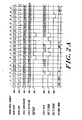
power supply 36 provides electrical operating power to all units of the system from the twobulk supplies bulk supply - FIG. 2A illustrates the foregoing operation with four pipelined multiple-phase transfer cycles on the bus structure for the FIG. 1
module 10.Waveforms clock 38 applies to theX bus 46, for twenty-one successive timing phases numbered (1) to (21) as labeled at the top of the drawing. The arbitration signals on the bus structure, represented withwave forms 58a, change at the start of each timing phase to initiate, in each of the twenty-one illustrated phases, arbitration for a new cycle as noted with the cycle-numbering legend # 1, #2, #3 ... #21. FIG. 2A also represents the cycle definition signals withwaveform 58b. The cycle definition signals for each cycle occur one clock phase later than the arbitration signals for that cycle, as noted with the cycle numbers on thewave form 58b. The drawing further represents the Busy, Data, A Bus Error, and B Bus Error signals. The bottom row of the drawing indicates the backplane mode in which the system is operating and shows transitions between different modes. - With further reference to FIG. 2A, during timing phase number (1), the
module 10 produces the cycle arbitration signals forcycle # 1. The system is operating in the Obey Both mode as designated. The Bus Master unit determined during the cycle arbitration of phase (1) defines the cycle to be performed during timing phase (2), as designated with thelegend # 1 on the cycledefinition signal waveform 58b. Also in timing phase (2), the arbitration for a second cycle,cycle # 2, is performed. - During timing phase (3) there is no response signal on the bus structure for
cycle # 1, which indicates that this cycle is ready to proceed with a data transfer as occurs during timing phase (4) and as designated with the <1 legend on the data waveform 58e. Also during timing phase (3), the cycle definition forcycle # 2 is performed and arbitration for afurther cycle # 3 is performed. - In timing phase (4), the data for
cycle # 1 is transferred, and the definition forcycle # 3 is performed. Also, a Bus A Error is asserted during this timing phase as designated withwaveform 58f. The error signal abortscycle # 2 and switches all units in the module to the Obey B mode. - The Bus A Error signal of timing phase (4) indicates that in the prior timing phase (3) at least one unit of the system detected an error regarding signals from the
A bus 42. The error occurred when no data was on the bus structure, as indicated by the absence of data in waveform 58e during timing phase (3), and there hence is not need to repeat a data transfer. - During timing phase (5), with the system operating in the Obey B mode, a fifth cycle is arbitrated, the function for
cycle # 4 is defined and no response signal is present on the bus structure forcycle # 3. Accordingly that cycle proceeds to transfer data during time phase (6), as FIG. 2A designates. - A
new cycle # 7 is arbitrated in timing phase (7) and the definition operation proceeds forcycle # 6. In time phase (8), a Busy signal is asserted. This signal is part of the response forcycle # 6 and aborts that cycle. - The arbitration and definition operations in time phase (9) follow the same pattern but another Bus A Error is asserted. The system already is operating in the Obey B mode and accordingly the response to this signal is simply to log the error.
- Further Bus A Error signals occurring during time phases (11), (12) and (14) again have no effect on the system other than to be logged, because the system is already operating in the Obey B mode.
-
Cycle # 12 is aborted by the Busy signal asserted during time phase (14). Data forcycle # 11 is transferred in the normal sequence during time phase (14). Further, the data transfer forcycle # 14 occurs in time phase (17). - In time phase (19), immediately following the
cycle # 15 data transfer of time phase (18), a Bus B Error is asserted. This error signal aborts cycle 117, which is in the response phase, and initiates a repeat of the data transfer forcycle # 15. The repeat transfer occurs duringcycle # 20. Further, this error signal switches the module to the Obey A mode. - Control logic in each unit of the FIG. 1
processor 10 provides the operations in that unit for executing the foregoing bus protocol which FIG. 2A illustrates. The protocol which control logic in each peripheral control unit includes conditions the unit, when first turned on, to receive signals on both theA bus 42 and theB bus 44 and to process the two sets of signals as if they are identical. Each illustrated central processor unit and memory unit, which process signals received from a single one of the duplicated buses, initially receives signals on theA bus 42, but operates as if the signals on the Bbus 44 are identical. Further, the control logic in all units initially conditions the unit to transmit signals identically on both the A and the B buses, in lock-step synchronism. - The control logic in each illustrated peripheral control unit responds to the A bus error signal and to the B bus error, transmitted on the
X bus 46, to condition the unit for the following operation. A Bus Error signal for the A (or B) bus causes the unit, and hence all units in a processor module, to stop receiving on both buses and to receive only on the other bus, i.e. the B (or A) bus, commencing with the first timing interval following the one in which the Bus Error signal first appears on the X bus. The units continue however to transmit signals on both the A and the B buses. - After a peripheral control unit has responded to an A (or B) Bus Error signal by switching to receiving on only the B (or A) bus, the control logic therein does not again switch in response to further Bus Error signals for the A (or B) bus; it essentially ignores the further error signals. However, the control logic responds to a B (or A) Bus Error signal by switching the unit to receive on the A (or B) bus, and it then ignores further B (or A) Bus Error signals.
- In the illustrated module, faulty information is transmitted on the A and/or B buses generally only by the central processing unit and by the memory unit. This is because the illustrated peripheral control units check for faults prior to transmitting information on the A and B buses. If a fault is detected, the control unit in question does not transmit information, and only the partner unit does.
- Further, each unit applies address and data signals on the A and B buses with parity which that unit generates. The memory unit serves, in the illustrated embodiment, to check bus parity and to drive the appropriate bus error line of the
X bus 46 during the timing interval immediately following the interval in which it detected the bus parity error. The memory unit also sets a diagnostic flag and requests a diagnostic interrupt. - All units of a module which arbitrate for access to the bus structure, as discussed further in the next section, include logic that checks for false operation of the bus arbitration logic and that drives the appropriate bus error line-=in the event of such a fault--on the interval following the detection of the fault. The unit also sets a diagnostic flag and requests a diagnostic interrupt.
- The bus protocol which control logic in each unit provides further conditions that unit to provide the following operation in response to a Bus Error signal for the bus which the unit is presently conditioned to receive. (These operations do not occur for a Bus Error signal for a bus which is not being received; as noted the unit essentially ignores such an error signal.) A unit which was transmitting cycle definition signals during the interval immediately preceding the one in which the Bus Error signal appears on the X bus re-initiates that cycle, including arbitration for the bus, if that cycle continues to be needed. This is because the Error signal causes any unit receiving the cycle definition signals to abort that cycle.
- A unit which was transmitting data signals during the timing interval immediately preceding the one in which the Bus Error signal appears on the bus repeats the data transmission two intervals after it was previously sent, i.e. on the interval following the one in which the Error Signal appears on the bus.
- A unit receiving definition data signals for a cycle and which is identified (addressed) by such signals responds to the Bus Error during the next interval by aborting that cycle.
- A unit which was receiving data signals during the interval immediately preceding the one in which the Bus Error signal appears on the bus ignores that data and receives a re-transmission of that data two intervals after the ignored one. An alternative is for the unit to receive and latch the data from both buses and use only the data from the good bus.
- When a unit simultaneously receives Bus Error signals for both the A and the B buses, which indicates a memory ECC error, the unit responds exactly as it does to a Bus Error signal for a single bus being received, as discussed above, except that it does not make any change in the bus(es) to which it is responding. Thus an ECC error aborts any cycle that was placing cycle definition signals on the bus in the preceding interval, and it causes any data transfer in that preceding interval to be repeated in the next interval following the ECC error.
- As FIG. 2A illustrates, the occurrence of a Busy signal aborts a cycle that was placing definition signals on the bus in the preceding interval.
- Control logic for implementing the foregoing bus protocol and related operations in the several units of a processor module for practice of this invention can be provided using conventional skills, and is not described further, other than as noted.
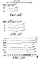
- FIG. 2B illustrates a timing sequence for a READ operation of
exemplary memory unit 16. As indicated by phase line 60a, an executing transfer cycle transmits definition signals defining the READ cycle in timinginterval # 1.Wave form 60b shows that during the latter half of timing interval <1, and continuing intotiming interval # 2, the memory unit strobes a memory chip array, i.e., a leaf, with a row address signal (RAS), causing row data to be transferred into temporary latches on each chip. During the latter half of timinginterval # 2, and continuing intotiming interval # 3, the memory unit strobes a column address signal (CAS),'pulling the addressed word from the temporary latches; seewave form 60c. The memory unit then transmits the word on the bus structure in timinginterval # 3, as indicated by phase line 60a. Simultaneously, theformat section 16e of the memory unit checks the data for error. In the event the data is erroneous, the memory unit asserts a BUS ERROR signal in timinginterval # 4 and transmits new data in timinginterval # 5. - The illustrated
memory unit 16 executes a WRITE operation according to the sequence shown in FIG. 2C. As indicated by phase line 62a, an executing transfer cycle defines a WRITE operation, including addressing information, during timinginterval # 1.Wave form 62b shows that the unit asserts RAS in the latter portion oftiming interval # 1 and proceeding throughtiming interval # 5. The memory unit asserts, CAS in timingintervals # 2 and #5, as shown by wave form 62c. According to wave form 62d, the memory units asserts a write signal, WRT, in timingintervals # 4 and #5. The concurrent assertion of CAS and WRT in timinginterval # 5 causes data applied from the bus during timinginterval # 3 to be stored at the address defined in the definition phase. In the event a BUS ERROR signal is received in timinginterval # 4, indicating that the data received in timinginterval # 3 was incorrect, the WRT signal and later CAS signal are delayed for two timing intervals. Similarly, RAS remains asserted for two additional intervals. - FIG. 2D illustrates a timing sequence for a REFRESH cycle utilized in
exemplary memory unit 16. As indicated bywave form 64a, a memory unit gate array (discussed below in conjunction with FIG. 5) asserts a JIFFY signal in timinginterval # 1. This signal indicates the necessity of refreshing at least a portion -- typically a row -- of the memory leaves. In response to this signal, a refresh request signal REF_REQ is asserted one cycle later, i.e., in timinginterval # 2; seewave form 64a. At this time, the refresh circuitry begins testing the backplane to determine when the refresh conditions are satisfied. These conditions are: - i) that none of the memory leaves are being addressed by a currently executing transfer cycle,
- ii) that leaves #0 and #1 are not currently being read, and
- iii) that leaves #0, #1, #2, and #3 are not currently being written.
- When the above conditions are satisfied, the refresh circuitry commences a refresh of the leaves. In the event these conditions are not satisfied within 7.25 microseconds, the refresh circuitry inhibits further memory access, thereby allowing refreshing to occur.
- In the illustration, the refresh cycle is indicated by
wave form 64c, beginning intiming interval # 8. Two timing intervals alter the refresh begins, the memory unit strobes leaves #0 and #1 with RAS, as indicated bywave form 64d. The content of a word stored in one of the leaves, e.g.,leaf # 0, is checked for error by strobing that leaf with CAS in the following timing interval, i.e., in timinginterval # 10; see wave form 64e. As further indicated by timing lines 64f and 64g, in timingintervals # 11 and #12, the memory unit strobes leaves #2 and #3, while simultaneously error-checking a word fromleaf # 2. The row address for refresh is determined by a refresh address latch in the memory gate array, discussed infra. Error checking is carried out byformal section 16e as described below. - To avoid conflict with transfers from other functional units, the memory unit asserts a BUSY signal in response to any attempt to address the memory leaves during the refresh cycle. According to
phase line 64h, a BUSY signal is asserted in response to any attempt to address memory leaves #0 - #3 during timing intervals #9 - #11. A BUSY signal is also asserted in response to an attempt to addressleaves # 2 or #3 intiming interval # 12. Thereafter, the all leaves are available for access by the system. - A memory unit operating according with the illustrated refresh timing cycles is capable of refreshing all of the memory locations in every 512 x 512 bit memory chip in the unit every four milliseconds. Such a unit is further capable of checking the memory for errors at the rate of one Mbyte per second. Within 32 seconds, the illustrated refresh mechanism is capable of refreshing and error-checking an entire 32 Mbyte memory board.
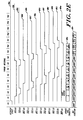
- FIG. 2E illustrates a timing sequence for a preferred memory unit update cycle executed according to a preferred practice of the invention. The sequence is executed by the partnered memory units of a duplicative pair when one of the units requires a memory content transfer from the other unit. This event typically occurs when a new memory unit,which replaces a prior faulty unit, requires loading in order to duplicate the original contents of the non-faulty memory unit.
- The illustrated update cycle is an extension of the refresh cycle normally executed by the memory unit. That is, the illustrated update cycle serves not only to refresh and error-check the chips at the address identified by the refresh latch, but also to transfer one word of information from each leaf of the original unit to corresponding locations in the new unit. Moreover, the sequence is executed without intervention of the central processor units. Timing for the sequence is determined -- as with the refresh cycle -- by the assertion of a JIFFY signal and concurrence of the refresh conditions.
- As indicated by wave form 66a, a refresh cycle signal is asserted in timing
interval 1 in response to prior assertion of a JIFFY signal and concurrence of the conditions set forth above. In the latter portion oftiming interval # 1, the update circuitry asserts RAS tostrobe leaf # 1; seewave form 66b, RAS remains asserted throughtiming interval # 7. As indicated bywave form 66c, the memory unit strobesleaf # 0 with CAS in timing interval qk2, causing the data stored in that leaf to be placed on the buses A and B during timinginterval # 3. While CAS is strobed in both the original and the new memory units, non-assertion of an ON-LINE flag associated with the new unit prevents that unit from asserting any data onto the bus during this period. Upon placement and initialization of the replacement memory board in thesystem 10, the operating system orders the memory board pair, i.e., the old, non-faulty and replacement boards, to begin the update process. The memory unit strobesleaf # 0 with WRT during timingintervals # 4 through #7, while strobing CAS in timinginterval # 7 to place bus data back intoleaf # 0, of both memory units; see wave form 66d. - As indicated by timing lines 66e-66g, the memory unit executes a similar sequence of RAS, CAS, and WRT to cause a word from
leaf # 1 of the original, non-faulty memory unit to be written to the new memory unit. Timing lines 66h-66j and 66k-66m illustrate like sequences for updatingleaves # 2 and #3. - . The transfer of data associated with the illustrated UPDATE cycle is illustrated by phase line 66n. Initially, in timing
interval # 2, the memory unit transfers a page status signal. This four-bit signal includes a one-bit flag indicating whether the page from which the transferred data is derived has been accessed, a one-bit flag indicating whether that page has been modified, and a two-bit code having values indicating whether the page is accessible, writeable, a test page, or a normal page. Thereafter, according to a illustrated embodiment, utilizing 72-bit memory words and a 32-bit data bus, in timinginterval # 3, the low order 32-bits of an update word fromleaf # 0 are transferred on the bus. The remainder of that word is transferred two timing intervals later, i.e., in timinginterval # 5. Interleaved with the transfer of information forleaf # 0, is the transfer of information forleaf # 1. To wit, the low-order bits of a word fromleaf # 1 are transferred duringtiming interval # 4, while the high-order bits are transferred duringtiming interval # 6. Similarly, the transfer of information fromleaves # 2 and #3 are interleaved during timing intervals #7 - #10, as indicated. - In the event of a bus error during the update cycle, the memory unit retransmits the sequence beginning with the word portion indicated on faulty. Thus for example, if a Bus error is asserted in timing
interval # 6, indicating a potential error in the prior transfer of the high order bytes of a word fromleaf # 0, the update circuitry will re-transmit these bytes in timinginterval # 7. The remaining transfer sequence, including the once-transmitted high order bytes fromleaf # 1, will be transmitted beginning intiming interval # 8 and proceeding throughtiming interval # 12. - Circuitry for implementing the aforementioned refresh and update cycles may be constructed utilizing the above timing diagrams with conventional memory design techniques. Schematics for one preferred refresh and update circuitry design are provided in Appendix A.
- In order to prevent other units of the date processing system from interfering with the update information transfer, the memory units ties the bus by asserting BUSY signals during the UPDATE cycle. The actions of the memory unit in this regard are illustrated by
phase line 660. Specifically, the memory unit prevents any other unit from utilizing the bus during timing intervals #0 - #8, by asserting successive ABORT signals. Operationally, these are non-specific BUSY signals, i.e., they are asserted regardless of which functional unit is addressed in a definition phase. During timingintervals # 9 and #10, the memory unit asserts a BUSY signal in response to an attempt to address memory leaves #2 or #3. Further, in timinginterval # 12, the memory unit asserts a BUSY signal in response to any attempt to addressmemory leaf # 3. - A memory unit operating with the illustrated Update timing sequence is capable of transferring 32 Mbytes of information between memory units in eight seconds, real time, regardless of system demand. This is to be distinguished from prior update mechanisms, discussed above, which required 16 seconds of central processor time, taking up to 30 minutes, real time, on a busy system.
- FIG. 3 shows a
main memory unit 16 of the FIG. 1processor module 10. Thepartner memory unit 18 is identical and operates in lock-step synchronism withunit 16. Thememory sections RAM 290 stores the upper half-word of a 64-bit data word and theRAM 292 stores the lower half-word of a 64-bit data word. Each RAM applies a half-word of read data through aninterleave multiplexor output multiplexor 298. The output from this multiplexor is applied to theA bus 42 by way of anA bus transceiver 300 and is applied to theB bus 44 through a B bus transceiver 302. Themultiplexors unit format section 16e, FIG. 1, which includes address and control circuits 16f shown in the lower part of FIG. 3. - Each
transceiver 300, 302 can apply different half-words of write data received from the associated bus to each of twowrite multiplexors RAM 290 by way of a data channel which has a further multiplexor 308, awrite register 310 and awrite buffer 312, and to write the lower half-word of the same data word in theRAM 292 by Way of a like data channel that has a further multiplexor 314, awrite register 316 and a write buffer 318. The twowrite multiplexors single transceiver 300, 302, and hence from either the A bus or the B bus. Information received during a 64-bit write cycle, as defined by the cycle's definition phase, is received in 32-bit portions during the two halves of the data transfer .phase. - As further shown in FIG. 3, read data from the
RAMs RAMs multiplexor 298 for application to both the A bus and the B bus by way of thetransceivers 300, 302. If the illustratedmemory unit 16 is executing a 64-bit read cycle, as defined in the definition phase, 32-bit halves of the read word are applied to the bus structure in each half of the data transfer phase. - A
parity checking circuit 328 is connected to check the parity of the write data output from thetransceiver 300, and a likeparity check circuit 330 is connected with the write data output from the transceiver 302. - A
check bit generators parity generator 342 connected to introduce a parity bit to each read data word output from themultiplexor 298 to thetransceivers 300, 302. - The
format section 16e of the illustrated memory unit further includes acomparator 326 connected to compare the data words output from thetransceivers 300, 302 to the half-word multiplexors clamp circuit 344, preferably identical in design and operation to the clamp circuits 88 and 90 in each central processing unit shown in FIG. 3, is connected to selectively ground the read data lines which feed to thetransceivers 300, 302. - It will thus be seen that the illustrated memory unit is in effect arranged with two identical read/write portions, each of which processes a 32-bit half-word of a given data word. Each such portion includes one
transceiver 300, 302, one busselect multiplexor - With further reference to FIG. 3, the address and control circuits 16f of the memory unit are similarly arranged in two portions, each of which operates with one
RAM Receivers 346 and 348 connect with the address and function conductors of theA bus 42 and of theB bus 44, respectively, and are connected withchannel multiplexors 350, 352 to select the signals from one receiver and correspondingly from one bus. An address andcontrol stage 354 receives the signals from the multiplexor 350 and applies them to an address andcontrol buffer 356 that operates theRAM 290. Similarly, an address andcontrol stage 358 receives signals from themultiplexor 352 for producing signals, which are applied by way of an address andcontrol buffer 360 to operate theother RAM 292. Thestages - A
comparator 362 is connected to compare the address and control signals output from the tworeceivers 346 and 348, i.e., on the twobuses data comparator 326, produces a fault signal. -
Parity check circuit receivers 346 and 348, respectively. The dataparity check circuit 328 and the addressparity check circuit 364 test the parity of signals on theA bus 42 for all data transfer operations of theprocessor module 10. Theparity check circuits B bus 44. Note that address parity is separate from data parity inasmuch as address signals, including function or cycle definition, and data signals occur at different phases of a cycle. In each phase each set of bus conductors has its own parity, which is tested. - The illustrated
memory unit 16 also has a status andcontrol stage 368 which is not duplicated. The stage receives the parity error signals, the comparator fault signals, and ECC syndrome signals from the ECC stages 320 and 321. Thestage 368 connects to numerous other elements in the memory unit, with connections which are in large part omitted for clarity of illustration. Abus error stage 370 is connected with thestage 368 and, by way a transceiver, with conductors of theX bus 46 as described below with reference to FIG. 4. - With this arrangement shown in FIG. 3, the
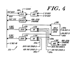
memory unit 16 can operation without a partner unit 18 (FIG. 1) and still detect and correct for a single failure in an integrated circuit chip of theRAMs unit 16 with apartner unit 18 is able to detect a high percentage of single component failures and to continue functioning by disabling the failingmemory unit memory unit bus structure 30 and signals other units of the system in the event that such an error is detected. This arrangement is deemed preferable, but other units can also be arranged to provide this operation, either in lieu of or in addition to the bus error-checking in the memory unit. Theparity check circuits comparators memory unit 16 can function as an I/O device which other units of theprocessor module 10 can address, for example to diagnose a detected fault in operation-of amemory unit - FIG. 4 shows the
bus error stage 370 of FIG. 3 which responds to parity error signals and the ECC syndrome signal of the illustratedmemory unit 26. An ORgate 372 receives the Data Parity Error signal for the A bus, which the parity check circuit 328 produces on itsoutput line 328a, and receives the Address Parity Error signal for the A bus output from theparity check circuit 364 online 364a. Similarly, the Data Parity Error signal for the B bus, produced online 330a, and the Address Parity Error signal for the B bus, produced online 366a, are applied to a further OR gate 374. Either error signal for the A bus and input to theOR gate 372 actuates atransceiver 376 to produce an A Bus Error signal. This signal is applied to theX bus 46 for communication to all units in themodule 10. Bimilarly, an error signal for the B bus and input to the OR gate 374 actuates afurther transceiver 378 to produce a B Bus Error signal that is applied to theX bus 46. FIG. 2A illustrates operation of the illustratedprocessor cnodule 10 when either Bus Error signal is asserted. - Each
transceiver control logic stage 380 that produces the OBEY A and OBEY B select signals for themultiplexors transceiver 376 applies the A Bus Error signal received from the bus structure, even when driven by thememory unit 16, to thelogic stage 380 and thetransceiver 378 likewise applies the B Bus Error signal. Thelogic stage 380 normally produces both OBEY signals. When it produces a single OBEY signal, and receives a Bus Error signal for the bus not being obeyed, it maintains the same single OBEY signal. However, when it produces a single OBEY signal and receives a Bus Error signal for the bus that is being obeyed, it switches to produce only the other OBEY signal. - The operation of the FIG. 3
check bit generators memory unit 16 receives from the bus structure has a 32-bit length plus one parity bit, introduced for example by the parity generator 92 in a CPU section described above. Theparity check circuits memory unit 16. Only 32 data bits of each input 64-bit word are applied to eachbus multiplexor multiplexor - The multiplexor 308, 314 selects 8, 16, 24, or 32 bits of new data and merges them into the required byte positions in the 64-bit word read from the RAM's via
multiplexor 298. The output of multiplexor 308, 314 is thus 64 bits and is fully duplicated. - The
check bit generator 340 adds to each 64-bit word, eight check bits to bring each word length to 72-bits, all of which are written in eachRAM memory 16 stores a 72-bit memory word for each 64-bit data world. The code with which these error checking and correcting bits are appended to each data word are set forth in the following Table I, in which the data word bits are numbered (63) through (00), and the memory check bits introduced by the check bit generator are numbered (7C) to (OC). The effectiveness of this ECC code stems in significant part from the fact that the present memory unit employs two half-word-processing portions, two half-word-storing RAMs, and controls each RAM with one of two identical address and control circuit portions. OneRAM 290 stores the data bits designated 63 to 32 and the check bits 7C, 6C, 5C, and 4C of the following code. Theother RAM 292 stores the data bits of 31 to 00 and thecheck bits 3C, 2C, 1C and OC. It is preferred that each data half-word of a memory word include the parity bit generated from the other half-word.


- When the
memory unit 16 is used without apartner unit 18, this eight-bit error correcting code of Table I makes possible the correction of single RAM failures. Further, when thememory unit 16 operates with apartner unit 18, the partnered units are capable of detecting errors in each unit and of isolating either unit from driving further signals onto the bus while the other unit continues normal operation. The eight-bit error code of Table I enables the source of a single bit error to be located. The status andcontrol stage 368 includes failure registers for storing the address of an error for subsequent accessing, and for storing the syndrome. - In the event of a non-zero syndrome, the
unit control stage 368, receives and processes diagnostic interrogation signals but does not drive signals onto the bus structure except in response to such interrogation. - Data routed through the
multiplexors 304, 308, thewrite register 310, and thecheck bit generator 340 is fully duplicated and checked by a comparator 336 after the check-bit generator, as illustrated. - The illustrated memory unit detects faults in the nondupiicated. portions, e.g., in the status and
control stage 368 or the parity generators, by means of maintenance software. However, an error in this portion of the memory unit is not by itself likely to produce erroneous data on either the A bus or B bus. - With further reference to FIGS. 3 and 4, the syndrome signals from the ECC stages 320, 321 are applied to the status and
control stage 368, as indicated. A non-zero syndrome signal actuates a driver 384 (FIG. 4) to produce a Fast ECC Error signal and apply it to theX bus 46. A non-zero syndrome signal also produces both the A Bus Error signal and the B Bus Error signal, from thetransceivers gate 382 to respond to a selected clock signal. - The
memory unit 16, as noted above, carries out the foregoing fault detection operations concurrently with memory read and write operations. In the event a fault is detected during a time phase when the memory unit is driving read data onto the bus, the non-zero syndrome signal from the ECC stage 320 causes thedriver 384 of FIG. 4 to produce the Fast ECC signal during the same time phase. This signal informs theCPU transceivers data registers - With further reference to FIG. 3, each address and
control stage control stage 368 is actuated by the two Bus signals to drive a transceiver 388 to produce a Fast Busy signal and the Busy signal discussed above with reference to FIG. 2A. A further ANDgate 390, FIG. 3, produces an Out Enable signal that enables thedata transceivers 300 and 302 only when both Driving Bus signals are present. With this arrangement, when the two channels of the address and control circuit 168 do not concurrently produce the Driving Bus signals, the memory unit is disabled from transferring data to the bus structure, as desired to prevent potentially faulty data from being transmitted to other units of the computer system. Theclamp stage 344 in a memory unit prevents potentially faulty data from being applied to thetransceivers 300, 302 in the event of a power supply failure. - A memory unit having the foregoing features of FIGS. 3 and 4 can execute numerous memory cycles. In a memory read cycle, the data read from memory is applied to the
bus structure 30 by way of thetransceivers 300, 302 in the same time phase as it is applied to the ECC stages 320, 321. In the event this stage produces a non-zero syndrome, the memory unit produces the Fast ECC signal during the same time phase and transmits it to thecentral processing unit 12, 14 (FIG. 1) by way of theX bus 46. The ECC stage produces the corrected data word and stores it in the old data registers 322, 324 for feeding to the bus structure by way of themultiplexor 298 and thetransceivers 300, 302 during a subsequent timing phase. - In addition to executing a conventional write operation of a full data word, the memory unit can perform a write operation with only partial data from the bus structure. For this operation, the address control portion of the memory unit does not receive both the Upper Data Valid and the Lower Data Valid signals, as occurs when a full data word is to be written, but receives only one of these control signals. In response to receiving only a single Data Valid signal, the memory unit first reads from the
RAMs - Another memory cycle which the
memory unit RAMs transceivers 300, 302 and to receive the same data from the bus structure and again write it at the same address, with a recomputing of all ECC bits. This memory operation is useful, for example, to duplicate the contents of one memory unit in a partner unit. That is, to bring one memory unit up to date with a partner memory unit, a system can read from the latter memory unit and place the resultant data on the bus structure, and write that data from the bus structure into the former memory unit at the same location. Any data read from the former memory unit is not driven onto the bus structure, by inhibiting the Output Enable signal of thetransceivers 300, 302 in that memory unit. The illustrated memory unit is thus capable of writing from an on-line memory unit to an off-line memory unit in one multi-phase memory cycle. - Memory access cycles are defined by four bits on the
system 10 backplane. These four bits, asserted during a definition phase, are referred to as FUNC bits and havebit positions 
- FIG. 5 depicts a preferred architecture for
memory format section 16e ofmemory unit 16. Thesection 16e is fabricated from a Fujitso 3900 gate array module. The illustratedsection 16e, including upper half-word processing sub-section 402 and lower half-word processing sub-section 404, operates in conjunction withmemory section section duplicates section 402 to permit continuous verification of the operation of that sub-section, while a second partner sub-section (not shown) duplicates the operation section of 404 to permit continuous verification of the operation of that sub-section. For clarity, the discussion below is directed tosection 402 and its interaction with the other sections. The construction and operation ofsection 404, as well as first and second partner sections, will be understood accordingly. - The
section 402 includes plural data latches designated LA, LB, LC, ... LK, having associated control lines, each designated as "L".Section 402 also includesmultiplexors buffers flop 416,comparator 418, error checking sections (ECC's) 420, 422,decode section 424, anderror correction section 426. - The
section 402 receives bus data viainterface sections line 428, branching to form an input to latch LF as well as tomultiplexor 406. An output of latch LF also forms an input tomultiplexor 406. A logical AND 431 of an INTERLOCK signal, received online 432, and an output of latch LC form another input tomultiplexor 406.Multiplexor 406 is controlled by a new data select signal received online 434. An output ofmultiplexor 406 is directed to-latch LG. An input to latch LK provides diagnostic test signals via line 440. Outputs from latch LG are directed to latch LH and ECC 420, as indicated. - An output of ECC 420, representing check bits for 32 data bits, is directed to latch LI. An output that latch is, in turn, directed to buffer 410. Check bits produced at the output of
buffer 410 are XOR'ed with check bits produced bysection 404 prior to their being written to RAM's 16a, 16b. - An output of latch LH is directed to
buffers comparator 418, having as one input the output of latch LH and having as another input the output from the first processing sub-section. An output fromcomparator 418 is directed to flip-flop 416. Another input to that flip-flop provides a strobe signal. An output of flip-flop 416 is to buffer 414. The output of that gate signals an ERROR condition in the event the comparator detected an inequality. - The
section 402 receives data and check-bits from RAM's 16a, 16b on data and check bits onlines 462 and 464, respectively. One output of latch LA is directed tomultiplexor 408, while the other is directed to ECC 422. An output from ECC 422 is directed togate 415, which generates a partial SYNDROME signal in the event an ECC error is detected. - A loop-
back line 470 forms a second input tomultiplexor 408 from latch LE. Control for themultiplexor 408 is signalled online 472 as aPHASE 5 REPEAT. An output frommultiplexor 408 is directed to latch LB, as an output from XOR 474, representing syndrome bits. A data output of latch is directed to correctingsection 426, while syndrome output of the latch is directed to decodesection 424. An output ofdecode section 424 forms a second input to correctingsection 426. - An output of the correcting
section 426, representing corrected data, is routed to latch LC. From there, the data is routed to ANDgate 431 and to latch LD. Data from latch LD is routed to latch LE, as indicated. - As noted above, lower half-
word processing sub-section 404 is constructed identically to upper half-word processing sub-section 402 and operates to process the low-order 36 bits of each 72-bit memory word. The sub-sections 402,404 interact in order to compute error-correcting and syndrome bits. In particular, error correcting bits output atbuffer 410 ofsection 402 are XOR'ed with corresponding bits output by the equivalent buffer ofsection 404. While the bits output bybuffer 410 represent only 32 of the data bits, the EXCLUSIVE OR of those bits with corresponding bits fromsection 404 provides error-correcting capability for a full 64 data bits. - As indicated by FIG. 5, the output of XOR 476 is directed to
buffers comparator 482. In the event of a mismatch of these compared signals, an error bit is generated atbuffer 486, after detection at flip-flop 484. - FIG. 5 also illustrates the computation of syndrome bits for words received from the RAM's. In particular, the output of
buffer 415 latches the eight syndrome bits for the 32 data bits received at latch LA. These eight syndrome bits are XOR'ed with eight corresponding bits generated insection 404 in order to produce eight error correcting bits. Six of these bits, revealing the location of the erroneous bits, are passed to latch LB, as indicated. - In addition to indicating the component structure of
section 16e, FIG. 5 illustrates the data path widths and signal timing forsections section 16e is indicated by way of an encircled numeral. Thus for example,section 402 receives a 32-bit input to latch LA online 462, while the section receives a four-bit input to latch LA on line 464. The remaining numeric indications of FIG. 5 indicate signal timing. Encircled indications of the form "x/yy", where x and y are integers, reveal time intervals in which signals are deemed stable. The "x" portion of the indicator relates to timing phases, while the "yy" portion relates to nanosecond intervals within the timing interval. Thus, for example, thePHASE 5 REPEAT signal received online 472 is stable inphase # 5 during the interval between the 15th and 125th nanosecond. Numeric indications at the latch controls reveal when signals placed on those controls are asserted. Thus, for example, thesection 402 asserts the latch LA control during the timing interval between 20 and 100 nanoseconds during each phase of operation. - FIG. 6 depicts an architecture for a preferred memory
unit gate array 500, providing an interface between thesystem bus structure memory unit sections first parity element 502 for checking the parity of signals received on theA bus 42. Asecond parity element 504 checks the parity of signals received on theB bus 44. Acomparator 506 compares signals received from bothbuses - The control register section is comprised of plural independently addressable 32-bit latches, including a
control latch 508, anerror address latch 510, analarm latch 512, and apage latch 514. Theexemplary control latch 508 stores information as follows:
- The
error address latch 510 is utilized to store addressing information, includingphase 3 address and error addresses. Thealarm latch 512 is a 16-bit register which is incremented every JIFFY cycle. Upon overflow, thelatch 512, if enabled by ALARM SET, causes an intterupt to be sent to the central processor units. Thepage latch 514 stores the address of the current page of interest. - The gate array addressing table section is comprised of independently addressable 32-bit latches, including
daytime latch 516,jiffy latch 518, seconds latch 520, and refreshaddress latch 522. The daytime latch stores a signal representative of the time of day. Thejiffy latch 518 stores, in its high-order bits, a signal representative of the number of elapsed JIFFY intervals. In its low-order bits, thelatch 518 stores a signal representative of elapsed clock system clock cycles, represented as "CNT". Together, the daytime and jiffy latches 516, 518 represent the time of day in 125 nanosecond intervals. - The seconds latch 520 includes a high-order section representing elapsed seconds. A mid-section represents JIFFY intervals, while a low-order section also represents elapsed system clock cycles. The
refresh address latch 522 stores a signal indicative of the address of the section of the RAM that is currently being refreshed. - In the illustrated embodiment, the daytime latch is referenced by
memory address 30; the jiffy latch is referenced bymemory address 34; the seconds latch is referenced bymemory address 38, and the refresh address latch is referenced by thememory address 3C. - The illustrated
gate array 500 includes, additionaly, routing circuitry for transmitting signals between the various elements. This routing circuitry includesmultiplexor 524, having inputs connected to BUSA address line 42, BUSB address line 44,refresh address register 522, and control andaddress multiplexor 526. Routing selected bymultiplexor 524 is determined by control lines 528a and 528b. - An output of
multiplexor 524 is directed to latch 528. The output of this latch is, in turn, directed toparity generator 530 and to buffer 532. The output ofelements - Signals transmitted from the memory unit proper to the
gate array 500 are received from LOCAL BUS C atbuffer 534. An output of this buffer is directed to local latch. This latch, in turn, is connected to the control and address latches 508-522, viamultiplexor 538. A second input tomultiplexor 538 is connected toincrementor 540 and its associatedlatch 542. An input to that latch ismultiplexor 544, which routes signals received from selected address and control latches 512 (address 28), 516 (address 30), 518 (address 34), and 522 (address 3C). - Information transmitted from the address and control latches is routed through
multiplexors multiplexor 526. - Aside from verifying addressing information received from the bus, the
array 500 permits memory-type access to address and control latches, including the daytime latch. Information stored in each of the address and control latches may be obtained by referencing, for example, in a definition phase, the memory unit with the address of the desired address or control latch. For example, the daytime latch may be referenced by sending to thememory unit address 30, causing the time-of-day information to be transferred via local bus C to the data output pins of the memory_unit. - The gate array circuitry also provides automatic incrementing of various latches in the addressing and control sections. At the outset, overflow from the CNT sections of each of the jiffy and seconds latches 518, 510 flows directly into the high-order sections of each of those latches. Accordingly, the jiffy section of
latch 518, as well as the jiffy and second sections oflatch 520, are automatically incremented. Moreover, whenever these CNT sections ready "FD" (hexadecimal), the increment circuitry 538-544, causes the refresh address to be incremented. Similarly, when CNT reaches "FF" (hexadecimal), the increment circuitry causes the jiffy latch to be incremented, while at "01" (hexadecimal), the daytime latch is incremented. Accordingly, the refresh and daytime latches remain up-to-date and available for access without intervention of the central processing unit or other outside control. - In a preferred embodiment, the
gate array 500 is arranged for generating a JIFFY signal every 15.25 microseconds. During memory testing stages, for example, the JIFFY cycle time can be lengthened, causing the RAM's to be refreshed less often and, thus, to fail with a frequency correlating to their integrity. - Upon insertion of a replacement memory board in the
system 10, as discussed above, the initialization sequence is effected. This sequence first involves stopping all counters in the memory system, including those contained ingate array 500. Next, the contents of the control register section and addressing table from the original, non-faulty memory unit are transferred to the partnered replacement board. This memory board pair is signalled to begin the update process, and the memory system counters are restarted.
Claims (8)
Priority Applications (1)
| Application Number | Priority Date | Filing Date | Title |
|---|---|---|---|
| AT87307179T ATE101935T1 (en) | 1986-08-14 | 1987-08-14 | DIGITAL DATA PROCESSING DEVICE. |
Applications Claiming Priority (2)
| Application Number | Priority Date | Filing Date | Title |
|---|---|---|---|
| US89666786A | 1986-08-14 | 1986-08-14 | |
| US896667 | 1986-08-14 |
Publications (3)
| Publication Number | Publication Date |
|---|---|
| EP0256864A2 true EP0256864A2 (en) | 1988-02-24 |
| EP0256864A3 EP0256864A3 (en) | 1989-11-08 |
| EP0256864B1 EP0256864B1 (en) | 1994-02-23 |
Family
ID=25406602
Family Applications (1)
| Application Number | Title | Priority Date | Filing Date |
|---|---|---|---|
| EP87307179A Expired - Lifetime EP0256864B1 (en) | 1986-08-14 | 1987-08-14 | Digital data processing apparatus |
Country Status (4)
| Country | Link |
|---|---|
| EP (1) | EP0256864B1 (en) |
| JP (1) | JPS63113641A (en) |
| AT (1) | ATE101935T1 (en) |
| DE (1) | DE3789128T2 (en) |
Citations (2)
| Publication number | Priority date | Publication date | Assignee | Title |
|---|---|---|---|---|
| US4371754A (en) * | 1980-11-19 | 1983-02-01 | Rockwell International Corporation | Automatic fault recovery system for a multiple processor telecommunications switching control |
| US4453215A (en) * | 1981-10-01 | 1984-06-05 | Stratus Computer, Inc. | Central processing apparatus for fault-tolerant computing |
-
1987
- 1987-08-14 AT AT87307179T patent/ATE101935T1/en not_active IP Right Cessation
- 1987-08-14 JP JP62201966A patent/JPS63113641A/en active Pending
- 1987-08-14 EP EP87307179A patent/EP0256864B1/en not_active Expired - Lifetime
- 1987-08-14 DE DE3789128T patent/DE3789128T2/en not_active Expired - Fee Related
Patent Citations (2)
| Publication number | Priority date | Publication date | Assignee | Title |
|---|---|---|---|---|
| US4371754A (en) * | 1980-11-19 | 1983-02-01 | Rockwell International Corporation | Automatic fault recovery system for a multiple processor telecommunications switching control |
| US4453215A (en) * | 1981-10-01 | 1984-06-05 | Stratus Computer, Inc. | Central processing apparatus for fault-tolerant computing |
Non-Patent Citations (2)
| Title |
|---|
| COMPUTER SYSTEMS, June 1985, pages 47-48,51; D. TAYLOR: "Failsafe computing" * |
| IBM TECHNICAL DISCLOSURE BULLETIN, vol. 24, no. 10, March 1982, pages 5188-5190, New York, US; A. BLUM: "Full use of transfer cycles in computers" * |
Also Published As
| Publication number | Publication date |
|---|---|
| JPS63113641A (en) | 1988-05-18 |
| DE3789128D1 (en) | 1994-03-31 |
| EP0256864B1 (en) | 1994-02-23 |
| ATE101935T1 (en) | 1994-03-15 |
| DE3789128T2 (en) | 1994-09-29 |
| EP0256864A3 (en) | 1989-11-08 |
Similar Documents
| Publication | Publication Date | Title |
|---|---|---|
| US4866604A (en) | Digital data processing apparatus with pipelined memory cycles | |
| US5005174A (en) | Dual zone, fault tolerant computer system with error checking in I/O writes | |
| US4916704A (en) | Interface of non-fault tolerant components to fault tolerant system | |
| EP0306244B1 (en) | Fault tolerant computer system with fault isolation | |
| US4907228A (en) | Dual-rail processor with error checking at single rail interfaces | |
| US5249187A (en) | Dual rail processors with error checking on I/O reads | |
| US4597084A (en) | Computer memory apparatus | |
| EP0077154B1 (en) | Digital data processor with high reliability and method | |
| US4750177A (en) | Digital data processor apparatus with pipelined fault tolerant bus protocol | |
| US5068851A (en) | Apparatus and method for documenting faults in computing modules | |
| US5153881A (en) | Method of handling errors in software | |
| US5345566A (en) | Method and apparatus for controlling dual bus system | |
| US5068780A (en) | Method and apparatus for controlling initiation of bootstrap loading of an operating system in a computer system having first and second discrete computing zones | |
| US5251227A (en) | Targeted resets in a data processor including a trace memory to store transactions | |
| US5048022A (en) | Memory device with transfer of ECC signals on time division multiplexed bidirectional lines | |
| US5065312A (en) | Method of converting unique data to system data | |
| US5163138A (en) | Protocol for read write transfers via switching logic by transmitting and retransmitting an address | |
| EP0411805B1 (en) | Bulk memory transfer during resync | |
| EP0416732B1 (en) | Targeted resets in a data processor | |
| EP0256864B1 (en) | Digital data processing apparatus | |
| EP0076654A1 (en) | Digital logic for priority determination |
Legal Events
| Date | Code | Title | Description |
|---|---|---|---|
| PUAI | Public reference made under article 153(3) epc to a published international application that has entered the european phase |
Free format text: ORIGINAL CODE: 0009012 |
|
| AK | Designated contracting states |
Kind code of ref document: A2 Designated state(s): AT BE CH DE ES FR GB GR IT LI LU NL SE |
|
| PUAL | Search report despatched |
Free format text: ORIGINAL CODE: 0009013 |
|
| AK | Designated contracting states |
Kind code of ref document: A3 Designated state(s): AT BE CH DE ES FR GB GR IT LI LU NL SE |
|
| 17P | Request for examination filed |
Effective date: 19900414 |
|
| 17Q | First examination report despatched |
Effective date: 19920825 |
|
| GRAA | (expected) grant |
Free format text: ORIGINAL CODE: 0009210 |
|
| AK | Designated contracting states |
Kind code of ref document: B1 Designated state(s): AT BE CH DE ES FR GB GR IT LI LU NL SE |
|
| PG25 | Lapsed in a contracting state [announced via postgrant information from national office to epo] |
Ref country code: SE Effective date: 19940223 Ref country code: NL Effective date: 19940223 Ref country code: GR Free format text: LAPSE BECAUSE OF FAILURE TO SUBMIT A TRANSLATION OF THE DESCRIPTION OR TO PAY THE FEE WITHIN THE PRESCRIBED TIME-LIMIT Effective date: 19940223 Ref country code: AT Effective date: 19940223 |
|
| REF | Corresponds to: |
Ref document number: 101935 Country of ref document: AT Date of ref document: 19940315 Kind code of ref document: T |
|
| REF | Corresponds to: |
Ref document number: 3789128 Country of ref document: DE Date of ref document: 19940331 |
|
| ET | Fr: translation filed | ||
| ITF | It: translation for a ep patent filed |
Owner name: BARZANO' E ZANARDO MILANO S.P.A. |
|
| PG25 | Lapsed in a contracting state [announced via postgrant information from national office to epo] |
Ref country code: ES Free format text: LAPSE BECAUSE OF FAILURE TO SUBMIT A TRANSLATION OF THE DESCRIPTION OR TO PAY THE FEE WITHIN THE PRESCRIBED TIME-LIMIT Effective date: 19940603 |
|
| NLV1 | Nl: lapsed or annulled due to failure to fulfill the requirements of art. 29p and 29m of the patents act | ||
| PG25 | Lapsed in a contracting state [announced via postgrant information from national office to epo] |
Ref country code: LU Free format text: LAPSE BECAUSE OF NON-PAYMENT OF DUE FEES Effective date: 19940831 |
|
| PLBE | No opposition filed within time limit |
Free format text: ORIGINAL CODE: 0009261 |
|
| STAA | Information on the status of an ep patent application or granted ep patent |
Free format text: STATUS: NO OPPOSITION FILED WITHIN TIME LIMIT |
|
| 26N | No opposition filed | ||
| PGFP | Annual fee paid to national office [announced via postgrant information from national office to epo] |
Ref country code: GB Payment date: 19990721 Year of fee payment: 13 |
|
| PGFP | Annual fee paid to national office [announced via postgrant information from national office to epo] |
Ref country code: CH Payment date: 19990723 Year of fee payment: 13 |
|
| PGFP | Annual fee paid to national office [announced via postgrant information from national office to epo] |
Ref country code: BE Payment date: 19990809 Year of fee payment: 13 |
|
| PG25 | Lapsed in a contracting state [announced via postgrant information from national office to epo] |
Ref country code: GB Free format text: LAPSE BECAUSE OF NON-PAYMENT OF DUE FEES Effective date: 20000814 |
|
| PG25 | Lapsed in a contracting state [announced via postgrant information from national office to epo] |
Ref country code: LI Free format text: LAPSE BECAUSE OF NON-PAYMENT OF DUE FEES Effective date: 20000831 Ref country code: CH Free format text: LAPSE BECAUSE OF NON-PAYMENT OF DUE FEES Effective date: 20000831 Ref country code: BE Free format text: LAPSE BECAUSE OF NON-PAYMENT OF DUE FEES Effective date: 20000831 |
|
| BERE | Be: lapsed |
Owner name: STRATUS COMPUTER INC. Effective date: 20000831 |
|
| GBPC | Gb: european patent ceased through non-payment of renewal fee |
Effective date: 20000814 |
|
| REG | Reference to a national code |
Ref country code: CH Ref legal event code: PL |
|
| PG25 | Lapsed in a contracting state [announced via postgrant information from national office to epo] |
Ref country code: FR Free format text: LAPSE BECAUSE OF NON-PAYMENT OF DUE FEES Effective date: 20010430 |
|
| REG | Reference to a national code |
Ref country code: FR Ref legal event code: ST |
|
| PGFP | Annual fee paid to national office [announced via postgrant information from national office to epo] |
Ref country code: FR Payment date: 20010725 Year of fee payment: 15 |
|
| PGFP | Annual fee paid to national office [announced via postgrant information from national office to epo] |
Ref country code: DE Payment date: 20010928 Year of fee payment: 15 |
|
| PG25 | Lapsed in a contracting state [announced via postgrant information from national office to epo] |
Ref country code: DE Free format text: LAPSE BECAUSE OF NON-PAYMENT OF DUE FEES Effective date: 20030301 |
|
| PG25 | Lapsed in a contracting state [announced via postgrant information from national office to epo] |
Ref country code: IT Free format text: LAPSE BECAUSE OF NON-PAYMENT OF DUE FEES Effective date: 20050814 |