EP0257101A1 - Switching regulator - Google Patents
Switching regulator Download PDFInfo
- Publication number
- EP0257101A1 EP0257101A1 EP87901650A EP87901650A EP0257101A1 EP 0257101 A1 EP0257101 A1 EP 0257101A1 EP 87901650 A EP87901650 A EP 87901650A EP 87901650 A EP87901650 A EP 87901650A EP 0257101 A1 EP0257101 A1 EP 0257101A1
- Authority
- EP
- European Patent Office
- Prior art keywords
- power source
- transformer
- winding
- switching
- primary winding
- Prior art date
- Legal status (The legal status is an assumption and is not a legal conclusion. Google has not performed a legal analysis and makes no representation as to the accuracy of the status listed.)
- Withdrawn
Links
Images
Classifications
-
- H—ELECTRICITY
- H02—GENERATION; CONVERSION OR DISTRIBUTION OF ELECTRIC POWER
- H02M—APPARATUS FOR CONVERSION BETWEEN AC AND AC, BETWEEN AC AND DC, OR BETWEEN DC AND DC, AND FOR USE WITH MAINS OR SIMILAR POWER SUPPLY SYSTEMS; CONVERSION OF DC OR AC INPUT POWER INTO SURGE OUTPUT POWER; CONTROL OR REGULATION THEREOF
- H02M3/00—Conversion of dc power input into dc power output
- H02M3/22—Conversion of dc power input into dc power output with intermediate conversion into ac
- H02M3/24—Conversion of dc power input into dc power output with intermediate conversion into ac by static converters
- H02M3/28—Conversion of dc power input into dc power output with intermediate conversion into ac by static converters using discharge tubes with control electrode or semiconductor devices with control electrode to produce the intermediate ac
- H02M3/325—Conversion of dc power input into dc power output with intermediate conversion into ac by static converters using discharge tubes with control electrode or semiconductor devices with control electrode to produce the intermediate ac using devices of a triode or a transistor type requiring continuous application of a control signal
- H02M3/335—Conversion of dc power input into dc power output with intermediate conversion into ac by static converters using discharge tubes with control electrode or semiconductor devices with control electrode to produce the intermediate ac using devices of a triode or a transistor type requiring continuous application of a control signal using semiconductor devices only
-
- H—ELECTRICITY
- H02—GENERATION; CONVERSION OR DISTRIBUTION OF ELECTRIC POWER
- H02M—APPARATUS FOR CONVERSION BETWEEN AC AND AC, BETWEEN AC AND DC, OR BETWEEN DC AND DC, AND FOR USE WITH MAINS OR SIMILAR POWER SUPPLY SYSTEMS; CONVERSION OF DC OR AC INPUT POWER INTO SURGE OUTPUT POWER; CONTROL OR REGULATION THEREOF
- H02M1/00—Details of apparatus for conversion
- H02M1/0083—Converters characterised by their input or output configuration
- H02M1/009—Converters characterised by their input or output configuration having two or more independently controlled outputs
Landscapes
- Engineering & Computer Science (AREA)
- Power Engineering (AREA)
- Dc-Dc Converters (AREA)
Abstract
In a DC-DC converter using an inverter, a series circuit consisting of a primary winding (N41) of a main power source transformer (T4), a first diode (45) and a switching means (2) is connected to a DC power source (1), and the primary winding (N51, N61) of a least one auxiliary transformer (Ts, Ts) and a second diode (55, 56) correspondent are connected in a parallel with a series circuit consisting of the primary winding (N41) of the main power source transformer (T4) and the first diode (45). Thus, a chopped voltage is applied to a plurality of transformers simultaneously by using a single switching control circuit (3) and a single switching means (2), so that a plurality of DC voltages can be outputted being inslated from each other.
Description
- The present invention relates to a switching regulator, more particularly, to a switching regulator for driving a power device using a plurality of mutually insulated DC power sources.
- Conventionally, a switching regulator is used for generating a plurality of mutually insulated DC power sources from one DC power source, for example, a power supply of an inverter device for driving an AC servomotor of an automated guided vehicle (AGV) by a battery source, as a power supply, in consideration of the factors of weight, conversion efficiency, and space occupied.
- In this conventional switching regulator, one switching control circuit and one switching transistor are used to generate a chopped voltage, the chopped voltage is applied to one power transformer, and a required DC power source is then generated.
- Note, an AC servomotor is generally used as a travelling motor or a lifting motor of the AGV, since it does not require a brush and has maintenance advantages. To drive and control the above AC servomotor, in addition to the main power source for a main control circuit, a driving power source insulated from the main power source is required.
- This driving power source is a power source for a driver circuit which amplifies a signal from a control circuit and drives high capacity power transistors, so that the AC servomotor is supplied with the controlled power source. The driving power sources are not only insulated from the control circuit, but also insulated from one another. For example, where one AC servomotor is driven by a three phase alternating current, six pairs of mutually insulated driving power sources are required for six driving transistors.
- As mentioned above, a conventional switching regulator uses one switching control circuit and one switching transistor, and a chopped voltage is applied to one transformer, so that the power supply generates a required DC power source. Therefore, for example, where one AC servomotor is driven by a three phase alternating current, six pairs of mutually insulated driving power sources are required, and thus many secondary windings for the six pairs of driving power sources must be wound on the one transformer.
- When a required number of secondary windings of the driving power sources are wound on one transformer, however, the weight of the transformer is increased and a printed substrate on which the transformer is mounted is liable to be damaged. Furthermore, the number of pins of the transformer is increased and the external form of the transformer becomes large. Additionally, many secondary windings are wound on the one transformer and many connecting pins are concentrated, so that many power lines must be led from the transformer position to other positions supplying the power sources. Further, so many connecting pins of the transformer are fixed on the printed substrate that the printed circuits become complex, and especially when a power source voltage is very high, a distance between the printed circuits must be enlarged to avoid a spark discharge therebetween. Consequently, the printed substrate must be enlarged and it is difficult to improve a packing density of the device.
- The object of the present invention is to provide a switching regulator using one switching control circuit and one switching means and applying chopped voltages to many transformers simultaneously, and generating many mutually insulated DC power sources, which is small in size and has simple printed circuits.
- According to the present invention, there is provided a switching regulator comprising: a power supply means; a switching means; a main power transformer, a primary winding of said main power transformer being connected to said power supply means via said switching means; a switching control circuit for detecting a voltage of one secondary winding of said main power transformer and controlling a duty ratio of said switching means; a first diode inserted in series with and in a forward direction to a primary winding of said main power transformer; at least one subsidiary power transformer, a primary winding of said subsidiary power transformer being connected in parallel with said primary winding of said main power transformer; and a second diode inserted in series with and in a forward direction to a primary winding of said at least one subsidiary power transformer.
- The switching regulator of the present invention uses one switching control circuit and one switching means and applies chopped voltages to many transformers simultaneously, and generates many mutually insulated DC power sources. That is, according to the switching regulator of the present invention, the one transformer having many windings is divided into many small transformers, so that the weight on the printed substrate is divided and the space occupied by the printed substrate on which the transformers are mounted, in decreased. Furthermore, the printed circuits are simplified, the printed substrate is miniaturized, and the packing density of the device is improved.
-
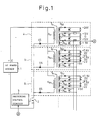
- Figure 1 is a block circuit diagram showing a part of an example of the switching regulator of the present invention; and
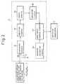
- Fig. 2 is a block diagram showing a switching control circuit.
- Figure 1 is a block circuit diagram showing a part of an example of the switching regulator of the present invention, wherein
reference numeral 1 denotes a DC power source,reference numeral 2 denotes a switching transistor,reference numeral 3 denotes a switching control circuit,reference numeral 4 denotes a main power source portion,reference numeral 5 denotes a first driving power source portion, andreference numeral 6 denotes a second driving power source portion. - The DC power source is a battery or an output of a rectifier circuit, the voltage E is applied to a primary winding N41 of a transformer (main power transformer) T4 in the main
power source portion 4 via theswitching transistor 2 and abreaking diode 45 for circulating current is inserted in series with and in a forward direction to the primary winding N41. The voltage E is also applied to a primary winding N51 of a transformer (subsidiary power transformer) T5 in the first drivingpower source portion 5 via theswitching transistor 2 and abreaking diode 55 for circulating current inserted in series with and in a forward direction to the primary winding N51. Furthermore, the voltage E is also applied to a primary winding N61 of a transformer (subsidiary power transformer) T6 in the second drivingpower source portion 6 via theswitching transistor 2 and abreaking diode 65 for circulating current inserted in series with and in a forward direction to the primary winding N61. In this way, the voltage E is applied to many driving power source portions, for example, where three AC servomotors are driven by a three phase alternating current, nine power source portions are provided in parallel. Further, theswitching control circuit 3 controls a ratio (duty ratio) between a switching ON time and a period of theswitching transistor 2 by making use of pulse width modulation (PWM). Thisswitching transistor 2 is driven by a high speed period, for example, a period of 40 KHz, and therefore, a MOS type FET can be used as theswitching transistor 2 to enable a high speed operation. - In the secondary side of the transformer T4 in the main
power source portion 4, there are provided secondary windings N42 , N43 and a secondary winding N44 for a controlled system power source, each secondary winding generates a required DC power source respectively by a rectifier diode and a smoothing condenser connected to each secondary winding. Concretely, for example, the secondary winding N42 supplies DC 24 Volts for use in an interface, the secondary winding N43 supplies DC +15 Volts for use in an analog differential amplifier, and the secondary winding N44 suppliesDC 5 Volts for use in a main power source of a speed control circuit in need of a high capacity. A part of an output of the secondary winding N44 for use in the main power source returns to theswitching control circuit 3 and controls a driving signal of theswitching transistor 2 in order to control the output voltage to a constant voltage. - In the secondary side of the transformer T5 in the first driving
power source portion 5, there are provided secondary windings N52 , NS3 and a regulating winding N54 of the controlled system power source, a rectifier diode and a smoothing condenser is connected to each of these windings, and each winding generates a required DC power source respectively. Concretely, for example, the secondary windings N52 and N53 supply DC 7.5 Volts and DC-4 Volts for use in one driving transistor, respectively. Where an AC servomotor is driven by a three phase alternating current, for example, three driving power source portions are required by one AC servomotor, since two driving transistors are used as one phase of the three phase alternating current. Therefore, where three AC servomotors are driven by a three phase alternating current, nine driving power source portions are provided in parallel with the power supply in order to drive a power device. - Further, in the secondary side of the transformer TS in the first driving
power source portion 5, there is provided the regulating winding N54 , and the number of turns of the regulating winding N54 is determined as an output voltage of the regulating winding N54 , as for an output of the secondary winding N44 for the controlled system power source. A rectifier diode and a smoothing condenser is connected to the regulating winding N54 , and the output voltage of the regulating winding N54 is applied to the output of the secondary winding N44 for the controlled system power source. Consequently, each output voltage of the secondary windings N52 and N53 in the first drivingpower source portion 5 is a constant voltage. When loads connected to these secondary windings N52 and N 53 have a low value, then the energy of the transformer TS is transferred through from the regulating winding N54 to the output of the secondary winding N44 for the controlled system power source. - The second driving
power source portion 6 is the same as the first drivingpower source portion 5; and in the secondary side of the transformer T6 , there are provided secondary windings N62 . N63 and a regulating winding N64 , so that constant voltages of DC power sources are generated by each winding. When loads of the secondary windings N62 . N63 have a low value, then the energy of the transformer T6 is transferred through from the regulating winding N64 to the output of the secondary winding N44. Such a driving power source portion is not only for the first drivingpower source portion 5 and the second drivingpower source portion 6, but also for many driving power source portions (for example, nine portions) connected in parallel therewith, as described above. - These driving power source portions are fixed on a printed substrate close to the driving transistor, the printed circuits required by each driving power source portions can be simplified by only connecting the primary windings and the regulating winding to each transformer, so that the printed substrate per se can be miniaturized. Since the one large transformer is divided into many small transformers, the number of connecting pins of each divided transformer is decreased. Consequently, the divided transformers can be miniaturized and the weight of the printed substrate on which the divided transformers are fixed can be spread. Furthermore, chopped voltages generated by one
switching control circuit 3 and oneswitching transistor 2 are applied to many transformers, and thus there is an advantage in a decrease of the cost of the power supply. - Figure 2 is a block diagram showing a switching control circuit.
- The controlled system power source (the output of the secondary winding N44 for the controlled system power source) of the main
power source portion 5, and the output (power source A) of the regulating winding N54 of the main power source portion and the output of the regulating winding N64 of the second drivingpower source portion 6 are returned to theswitching control circuit 3. Next, the power source A (for example,DC 5 Volts) is compared with a voltage E (for example,DC 5 Volts of a constant-voltage) of a reference power source 31 in acomparator circuit 32. An output of thecomparator circuit 32 is amplified by anamplifier circuit 33 and transferred to a photo-coupler 34. This photo-coupler 34 is used for floating the output of theamplifier circuit 33, and the output of the photo-coupler 34 is amplified by anamplifier circuit 35 and is transferred to a dutyratio control circuit 37 as an input signal. The dutyratio control circuit 37 generates a prescribed pulse width signal which is determined by a constant period sawtooth wave signal generated by asawtooth generating circuit 36 and by an output of theamplifier circuit 35, so that the ratio (duty ratio) between a switching ON time and a period of theswitching transistor 2 is determined by the output signal of the dutyratio control circuit 37. - Next, an operation of the example of the switching regulator of the present invention is described below.
- First, when the
switching transistor 2 is switched ON by the driving signal of theswitching control circuit 3, then the voltage E of theDC power source 1 is applied to the primary winding N41 of the transformer T4 through a breaking diode for controlling a circulatingcurrent 45, to the primary winding N51 of the transformer T5 through a breaking diode for controlling a circulatingcurrent 55, and to the primary winding N61 of the transformer T6 through a breaking diode for controlling a circulatingcurrent 65 respectively. Therefore, in the secondary windings N42 ' N43 and the secondary winding N44 for the controlled system power source of the transformer T4 , the secondary windings N52 . N53 and the regulating winding N54 of the transformer T5 ' and the secondary windings N62 . N63 and the regulating winding N64 of the transformer T6 , an induced voltage is provided in each winding respectively at the side marked with a dot ".". But electrical conduction does not occur, since each rectifier diode is inserted in a reverse direction. In this condition, an electric power is not transferred to each output side of the windings, but the energy is stored in the transformers T4 , T5 and T 6. - After a constant period, the
switching transistor 2 is switched OFF, then the polarity of the voltages applied to the transformers T4 , T5 and T6 is inverted, and electrical conduction occurs in the rectifier diodes of the secondary windings N42 N43 and the secondary winding N44 for controlled system power source of the transformer T4 , in the rectifier diodes of the secondary windings N52 , N53 and the regulating winding N54 of the transformer T5 , and in the rectifier diodes of the secondary windings N62 , N63 and the regulating winding N64 of the transformer T6 , so that the energy stored in the tranformers T4 , T5 and T6 is transferred to the smoothing condenser and to the output of each winding respectively. In the primary winding N41 of the transformer T4 , the primary winding N51. of the transformer T5 . and the primary winding N61 of the transformer T6 , thebreaking diodes switching transistor 2 is cut off), therefore the energy stored in the transformers T 4 , T5 and T6 is not transferred to the primary windings N41 . N51 and N61 respectively. - In this way, in the main
power source portion 4, the first drivingpower source portion 5 and the second drivingpower source portion 6, the required DC power sources can be given in accordance with the number of turns of each secondary winding. - Note, as in the above description, the power source a returned to the
switching control circuit 3 is not only connected to the output of the secondary winding N44 for controlled system power source in themain power source 4, but also to the output of the regulating winding N54 in the first drivingpower source portion 5 and to the output of the regulating winding N64 in the second drivingpower source portion 6. Consequently, the outputs of the secondary windings N52 , N 53 of the transformer T5 and the secondary windings N62 ' N63 of the transformer T6 can be stabilized, and the secondary windings N42 ' N43 of the transformer T also can be stabilized. Furthermore, when the power consumption of the first drivingpower source portion 5 or the second drivingpower source portion 6 is low, the excessive energy in the regulating winding N54 of the transformer T5 or the regulating winding N64 of the transformer T6 is transferred to the secondary winding N44 for controlling the system power source respectively. - In accordance with the present invention as described above, the switching regulator of the present invention uses one switching control circuit and one switching means and applies chopped voltages many transformers simultaneously, and generates many mutually insulated DC power sources. Therefore, the transformers can be small size and the printed circuit can be simplified, the space occupied by the printed substrate on which the transformers are fixed can be reduced and miniaturized, and furthermore, there is an advantage of a decreased in the cost of the power supply.
Claims (3)
1. A switching regulator comprising:
a power supply means;
a switching means;
a main power transformer, a primary winding of said main power transformer being connected to said power supply means via said switching means;
a switching control circuit for detecting a voltage of one secondary winding of said main power transformer and controlling a duty ratio of said switching means;
a first diode inserted in series with and in a forward direction to a primary winding of said main power transformer;
at least one subsidiary power transformer, a primary winding of said subsidiary power transformer being connected in parallel with said primary winding of said main power transformer; and
a second diode inserted in series with and in a forward direction to a primary winding of said at least one subsidiary power transformer.
2. A switching regulator according to claim 1, wherein said at least one subsidiary power transformer includes a regulating winding connected to said one secondary winding of said main power transformer.
3. A switching regulator according to claim 1, wherein said switching regulator is used for driving a power device.
Applications Claiming Priority (2)
| Application Number | Priority Date | Filing Date | Title |
|---|---|---|---|
| JP61037475A JPS62196071A (en) | 1986-02-24 | 1986-02-24 | Driving power source for power device |
| JP37475/86 | 1986-02-24 |
Publications (2)
| Publication Number | Publication Date |
|---|---|
| EP0257101A1 true EP0257101A1 (en) | 1988-03-02 |
| EP0257101A4 EP0257101A4 (en) | 1988-06-23 |
Family
ID=12498546
Family Applications (1)
| Application Number | Title | Priority Date | Filing Date |
|---|---|---|---|
| EP19870901650 Withdrawn EP0257101A4 (en) | 1986-02-24 | 1987-02-23 | Switching regulator. |
Country Status (5)
| Country | Link |
|---|---|
| US (1) | US4809151A (en) |
| EP (1) | EP0257101A4 (en) |
| JP (1) | JPS62196071A (en) |
| KR (1) | KR880701034A (en) |
| WO (1) | WO1987005165A1 (en) |
Cited By (3)
| Publication number | Priority date | Publication date | Assignee | Title |
|---|---|---|---|---|
| EP0410866A1 (en) * | 1989-07-28 | 1991-01-30 | Bull S.A. | Multioutput power converter |
| EP0609900A2 (en) * | 1993-02-05 | 1994-08-10 | The Lincoln Electric Company | Inverter power supply for welding |
| ES2101640A1 (en) * | 1994-10-24 | 1997-07-01 | Telefonica Nacional Espana Co | DC/DC converter for power feeding |
Families Citing this family (26)
| Publication number | Priority date | Publication date | Assignee | Title |
|---|---|---|---|---|
| FR2618957B1 (en) * | 1987-07-31 | 1989-11-17 | Dassault Electronique | POWER SUPPLY DEVICE, PARTICULARLY FOR A WAVE GENERATOR FOR A PULSE RADAR |
| DE3906600A1 (en) * | 1989-03-02 | 1990-09-13 | Vogt Electronic Ag | SWITCHING POWER SUPPLY |
| US5113337A (en) * | 1991-02-08 | 1992-05-12 | General Electric Company | High power factor power supply |
| FR2691853B1 (en) * | 1992-06-01 | 2002-12-20 | Smh Man Services Ag | Apparatus for charging a rechargeable electric energy accumulator. |
| DE4426017C2 (en) * | 1994-07-22 | 1998-01-29 | Walter Dr Ing Soehner | Power supply device, in particular battery charger for electric vehicles or the like |
| US7269034B2 (en) | 1997-01-24 | 2007-09-11 | Synqor, Inc. | High efficiency power converter |
| JPH10295079A (en) * | 1997-04-18 | 1998-11-04 | Yaskawa Electric Corp | Multi-shaft power supply circuit of transistor inverter device and its unit circuit |
| JP3280641B2 (en) * | 1999-09-08 | 2002-05-13 | 長野日本無線株式会社 | Energy transfer device |
| EP1047172A3 (en) * | 1999-04-21 | 2001-05-23 | Nagano Japan Radio Co., Ltd. | Energy transfer unit, charge unit, and power supply unit |
| JP3280635B2 (en) * | 1999-04-21 | 2002-05-13 | 長野日本無線株式会社 | Energy transfer device and power storage system |
| JP2004080851A (en) * | 2002-08-09 | 2004-03-11 | Aisin Aw Co Ltd | Power unit for drive |
| JP4193536B2 (en) * | 2003-03-24 | 2008-12-10 | 横河電機株式会社 | Switching power supply |
| DK2036189T3 (en) * | 2006-06-01 | 2019-05-27 | Google Llc | Continuous power distribution architecture for a data center |
| JP4208018B2 (en) | 2007-02-16 | 2009-01-14 | サンケン電気株式会社 | DC converter |
| US8080900B2 (en) * | 2007-07-18 | 2011-12-20 | Exaflop Llc | Direct-coupled IT load |
| CN103036443A (en) * | 2011-09-30 | 2013-04-10 | 台达电子企业管理(上海)有限公司 | Active multichannel isolated output power supply |
| US8193662B1 (en) | 2011-10-17 | 2012-06-05 | Google Inc. | Power supply source blending and smoothing |
| US9032250B1 (en) | 2012-11-05 | 2015-05-12 | Google Inc. | Online testing of secondary power unit |
| DE102012222934A1 (en) * | 2012-12-12 | 2014-06-12 | Siemens Aktiengesellschaft | Power supply device for several galvanically separated consumers |
| US10199950B1 (en) | 2013-07-02 | 2019-02-05 | Vlt, Inc. | Power distribution architecture with series-connected bus converter |
| US20150280580A1 (en) * | 2014-03-28 | 2015-10-01 | Hep Tech Co., Ltd. | Power conversion apparatus |
| JP6515549B2 (en) * | 2015-01-22 | 2019-05-22 | 富士電機株式会社 | Multi-output power supply |
| JP6438858B2 (en) * | 2015-07-03 | 2018-12-19 | 日立オートモティブシステムズ株式会社 | Power converter |
| WO2017203666A1 (en) * | 2016-05-26 | 2017-11-30 | 三菱電機株式会社 | Flyback power supply, inverter, and electric vehicle |
| CN111684698A (en) * | 2018-08-06 | 2020-09-18 | 深圳配天智能技术研究院有限公司 | Switching power supply of electric automobile and on-vehicle air conditioner compressor |
| JP2023128079A (en) * | 2022-03-02 | 2023-09-14 | 株式会社デンソー | Isolated power supply device |
Citations (2)
| Publication number | Priority date | Publication date | Assignee | Title |
|---|---|---|---|---|
| JPS55136872A (en) * | 1979-04-11 | 1980-10-25 | Nec Corp | Multiple-outputs switching regulator |
| EP0140580A2 (en) * | 1983-09-26 | 1985-05-08 | Farnell Instruments Limited | Power supply |
Family Cites Families (6)
| Publication number | Priority date | Publication date | Assignee | Title |
|---|---|---|---|---|
| US3569818A (en) * | 1969-07-22 | 1971-03-09 | Hughes Aircraft Co | Multiple output dc voltage regulator |
| JPS5840912B2 (en) * | 1978-11-16 | 1983-09-08 | 横河電機株式会社 | Multi-stage DC/DC converter |
| IE49593B1 (en) * | 1979-05-18 | 1985-10-30 | Gen Electric Co Ltd | Transistor switching circuit |
| JPS58162783A (en) * | 1982-03-20 | 1983-09-27 | Toyoda Autom Loom Works Ltd | Swash plate type variable displacement compressor |
| JPS58162783U (en) * | 1982-04-21 | 1983-10-29 | 日本ビクター株式会社 | switching power supply circuit |
| JPS5959085A (en) * | 1982-09-28 | 1984-04-04 | Toshiba Electric Equip Corp | Power source |
-
1986
- 1986-02-24 JP JP61037475A patent/JPS62196071A/en active Pending
-
1987
- 1987-02-23 WO PCT/JP1987/000118 patent/WO1987005165A1/en not_active Application Discontinuation
- 1987-02-23 KR KR1019870700973A patent/KR880701034A/en not_active Application Discontinuation
- 1987-02-23 US US07/124,798 patent/US4809151A/en not_active Expired - Fee Related
- 1987-02-23 EP EP19870901650 patent/EP0257101A4/en not_active Withdrawn
Patent Citations (2)
| Publication number | Priority date | Publication date | Assignee | Title |
|---|---|---|---|---|
| JPS55136872A (en) * | 1979-04-11 | 1980-10-25 | Nec Corp | Multiple-outputs switching regulator |
| EP0140580A2 (en) * | 1983-09-26 | 1985-05-08 | Farnell Instruments Limited | Power supply |
Non-Patent Citations (2)
| Title |
|---|
| PATENT ABSTRACTS OF JAPAN, vol. 5, no. 7 (E-41)[679], 17th January 1981; & JP-A-55 136 872 (NIPPON DENKI K.K.) 25-10-1980 * |
| See also references of WO8705165A1 * |
Cited By (6)
| Publication number | Priority date | Publication date | Assignee | Title |
|---|---|---|---|---|
| EP0410866A1 (en) * | 1989-07-28 | 1991-01-30 | Bull S.A. | Multioutput power converter |
| FR2650410A1 (en) * | 1989-07-28 | 1991-02-01 | Bull Sa | MULTI-OUTPUT ENERGY CONVERTER DEVICE |
| US5038265A (en) * | 1989-07-28 | 1991-08-06 | Bull S.A. | Power supply with multiple outputs and load balancing |
| EP0609900A2 (en) * | 1993-02-05 | 1994-08-10 | The Lincoln Electric Company | Inverter power supply for welding |
| EP0609900A3 (en) * | 1993-02-05 | 1994-10-19 | Lincoln Electric Co | Inverter power supply for welding. |
| ES2101640A1 (en) * | 1994-10-24 | 1997-07-01 | Telefonica Nacional Espana Co | DC/DC converter for power feeding |
Also Published As
| Publication number | Publication date |
|---|---|
| KR880701034A (en) | 1988-04-22 |
| EP0257101A4 (en) | 1988-06-23 |
| WO1987005165A1 (en) | 1987-08-27 |
| JPS62196071A (en) | 1987-08-29 |
| US4809151A (en) | 1989-02-28 |
Similar Documents
| Publication | Publication Date | Title |
|---|---|---|
| US4809151A (en) | Switching regulator having parallel diode isolated primary windings and plural secondary windings | |
| US6426884B1 (en) | Reducing reverse currents in a synchronous rectifier circuit | |
| KR100471093B1 (en) | Power supply device | |
| EP0243061A2 (en) | Off-line switcher with battery reserve | |
| US5717303A (en) | DC motor drive assembly including integrated charger/controller/regenerator circuit | |
| US20060007717A1 (en) | Switching power supply with direct conversion off AC power source | |
| CN204947890U (en) | Gate drive power system | |
| US4502104A (en) | Bootstrapped AC-DC power converter | |
| US9866129B2 (en) | Power conversion device including primary inverter, transformer, secondary converter, and controller | |
| US5282122A (en) | High voltage power supply topology suited for miniaturization | |
| EP2040365B1 (en) | Forward converter with self-driven synchronous rectifiers | |
| JP5332031B2 (en) | Switching control method for transformer coupled booster | |
| US6104623A (en) | Multiple output converter having secondary regulator using self-driven synchronous rectifiers | |
| JP7070830B2 (en) | Switching power supply | |
| CN101847930A (en) | Converter, switching power supply, and image forming apparatus | |
| US4455596A (en) | Flyback-forward boost switchmode converter | |
| US4752705A (en) | Off-gate circuit for a GTO thyristor | |
| JPH0787731A (en) | Dc/dc converter | |
| EP1440501B1 (en) | Motor control circuit and associated full bridge switching arrangement | |
| EP0607246B1 (en) | Regulated auxiliary power supply | |
| US4588906A (en) | Regulator circuit | |
| GB2243961A (en) | DC-DC Power supply circuit | |
| US5666281A (en) | Battery polarity switch for applying power to a co-axial cable and incorporating regulation | |
| JPH0740785B2 (en) | Multi-channel inverter circuit | |
| JP2003299367A (en) | Inverter |
Legal Events
| Date | Code | Title | Description |
|---|---|---|---|
| PUAI | Public reference made under article 153(3) epc to a published international application that has entered the european phase |
Free format text: ORIGINAL CODE: 0009012 |
|
| 17P | Request for examination filed |
Effective date: 19871113 |
|
| AK | Designated contracting states |
Kind code of ref document: A1 Designated state(s): DE FR GB |
|
| A4 | Supplementary search report drawn up and despatched |
Effective date: 19880623 |
|
| STAA | Information on the status of an ep patent application or granted ep patent |
Free format text: STATUS: THE APPLICATION HAS BEEN WITHDRAWN |
|
| 18W | Application withdrawn |
Withdrawal date: 19891215 |
|
| RIN1 | Information on inventor provided before grant (corrected) |
Inventor name: OTA, NAOTO |