EP0261685A2 - Microprocessor system - Google Patents
Microprocessor system Download PDFInfo
- Publication number
- EP0261685A2 EP0261685A2 EP87113998A EP87113998A EP0261685A2 EP 0261685 A2 EP0261685 A2 EP 0261685A2 EP 87113998 A EP87113998 A EP 87113998A EP 87113998 A EP87113998 A EP 87113998A EP 0261685 A2 EP0261685 A2 EP 0261685A2
- Authority
- EP
- European Patent Office
- Prior art keywords
- coprocessor
- data transfer
- master processor
- instruction
- data
- Prior art date
- Legal status (The legal status is an assumption and is not a legal conclusion. Google has not performed a legal analysis and makes no representation as to the accuracy of the status listed.)
- Granted
Links
Images


Classifications
-
- G—PHYSICS
- G06—COMPUTING; CALCULATING OR COUNTING
- G06F—ELECTRIC DIGITAL DATA PROCESSING
- G06F13/00—Interconnection of, or transfer of information or other signals between, memories, input/output devices or central processing units
- G06F13/14—Handling requests for interconnection or transfer
-
- G—PHYSICS
- G06—COMPUTING; CALCULATING OR COUNTING
- G06F—ELECTRIC DIGITAL DATA PROCESSING
- G06F9/00—Arrangements for program control, e.g. control units
- G06F9/06—Arrangements for program control, e.g. control units using stored programs, i.e. using an internal store of processing equipment to receive or retain programs
- G06F9/30—Arrangements for executing machine instructions, e.g. instruction decode
- G06F9/30003—Arrangements for executing specific machine instructions
- G06F9/3004—Arrangements for executing specific machine instructions to perform operations on memory
- G06F9/30043—LOAD or STORE instructions; Clear instruction
-
- G—PHYSICS
- G06—COMPUTING; CALCULATING OR COUNTING
- G06F—ELECTRIC DIGITAL DATA PROCESSING
- G06F9/00—Arrangements for program control, e.g. control units
- G06F9/06—Arrangements for program control, e.g. control units using stored programs, i.e. using an internal store of processing equipment to receive or retain programs
- G06F9/30—Arrangements for executing machine instructions, e.g. instruction decode
- G06F9/38—Concurrent instruction execution, e.g. pipeline, look ahead
- G06F9/3877—Concurrent instruction execution, e.g. pipeline, look ahead using a slave processor, e.g. coprocessor
Definitions
- the present invention relates to a microprocessor system, and in particular, to a data transfer control technology therein, for example, to a technology effectively applicable to a data transfer control of a data transfer between a plurality of registers included in a coprocessor and external storage means.
- a coprocessor is connected to a master processor such as a general-purpose data processor to enable a register set and an instruction set to be expanded, thereby adding a new processing capability to the processor.
- a master processor such as a general-purpose data processor to enable a register set and an instruction set to be expanded, thereby adding a new processing capability to the processor.
- the coprocessor monitors the instruction execution state of the master processor by use of a status signal.
- the instruction is caused to be executed by the coprocessor, and if a bus access is necessary at the execution of the instruction, the coprocessor operates as a local bus master in place of the master processor so as to generate a bus access cycle.
- the main processor is to detect an instruction for the coprocessor and to execute all bus cycles for a transfer of a command for the coprocessor and for a transfer of data between the memory and the coprocessor.
- the present inventors have discussed a case where the coprocessor effects transfer of a plurality of data items to and from the master processor and the memory in a system as described above in which the master processor executes the bus access cycle for the coprocessor, for example, including an operation to send an address signal to the memory.
- the system since the system has a characteristic that the master processor generates and controls the bus access cycle and the coprocessor, on the other hand, achieves a transfer of actual data, in a case where only the master processor recognizes and controls a sequence of data transfers, it has been found that a command must be issued to the coprocessor for each data transfer and that the efficiency of a sequence of data transfers is reduced because of the increase of the command issuances.
- the master processor cannot recognize by itself a condition whether or not the necessary transfer cycle has been finished, and hence the master processor must obtain an information indicating the end of a sequence of data transfer cycles from the coprocessor.
- the transfer of the information is undesirably delayed in a local signal line and a data input/output buffer, that the initiation of the subsequent operation to be executed after the sequence of data transfers is delayed, and that the operation efficiency of the overall system is therefore lowered.
- the coprocessor when the coprocessor effects a sequence of transfers of plural data items to and from the master processor and the memory according to the bus access cycle initiated by the master processor, the coprocessor is provided therein an information indication a data storage location which is a data transfer source or a data transfer destination; furthermore, the master processor and the coprocessor independently monitor the transfer operations to detect the end of the sequence of data transfer operations.
- the information necessary for the bus access cycle initiated by the master processor can be contained in a data transfer instruction; moreover, the information included in the data transfer instruction can be supplied as a data transfer command to the coprocessor.
- the end of the sequence of data transfer operations independently monitored by the master processor and the coprocessor can be notified according to the field information indicating a plurality of data storage locations in the coprocessor, said field information being included in the data transfer instruction and the data transfer command.
- the coprocessor when executing a sequence of plural data transfer operations, the coprocessor need not receive the command from the master processor each time a data item is transferred; moreover, the coprocessor need not notify the master processor the end of the sequence of data transfer cycles. Consequently, in a case where the processor generates and controls the bus access cycle on one hand and the coprocessor effects the actual data communication on the other hand, the system achieves to prevent the condition that leads to the minimization of the data transfer efficiency due to the increase of the command issuances, which may occur when only the master processor recognizes and controls the sequence of data transfers.
- system further effects to prevent the situation that the supply of the end indication of the sequence of data transfer cycles to the master processor is undesirably delayed, which may take place when only the coprocessor recognizes and controls the sequence of data transfers.
- improvement of the efficiency of the sequence of data transfers is realized; furthermore, the next operation necessary to be executed after the data transfer operation can be immediately initiated, thereby achieving the improvement of the operation efficiency of the overall system.
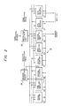
- the microprocessor system of FIG. 1 although not limited to, comprises a master processor 1 such as a general-purpose processor and a coprocessor 2 closely linked thereto by means of a local bus 3, the coprocessor 2 having functions including the floating operation, the multiprecision operation of a transcendental function, and so forth.
- the local bus 3 is linked via a system interface 4 to a system bus 5.
- the system is representatively linked to a memory 6 comprising, although not limited to, a random access memory (RAM).
- RAM random access memory
- a macro instruction such as a machine language instruction supplied from the system side is fetched by the master processor 1.
- the master processor 1 although not limited to, separates therefrom fields necessary for the coprocessor 2 to generate a command and then supplies the command to the coprocessor 2.
- the master processor 1 controls all bus cycles at a transfer of a command to the coprocessor 2, a data transfer between the memory 6 and the coprocessor 2, and so forth.
- the master processor 1 is provided with a micro ROM 7 in which microprograms are stored.
- the micro ROM 7 is accessed from the micro address decoder 8, which causes micro instructions constituting the microprograms to be sequentially read.
- reference numeral 9 indicates an instruction fetch unit including an FIFO register (not shown) used to prefetch a macro instruction according to a pipeline processing or an instruction prefetch control.
- the micro address decoder 8 is supplied with an address signal obtained by decoding in an instruction decoder 10 an operation code of the macro instruction fetched into the instruction fetch unit 9.
- the micro address decoder 8 decodes the address signal to read from the micro ROM 7 the first instruction among a sequence of micro instructions to execute the macro instruction.
- the micro instruction thus read is supplied to the micro instruction decoder 11 and is decoded therein.
- the micro instruction decoder 11 supplied control signals necessary for the execution of the instruction to the execution unit 12.
- the instruction decoder 10 includes a multiplexer (not shown) effecting for an output a selection between a macro instruction and a code of the next address field included in a micro instruction. Consequently, based on the code of the next address field thus sequentially selected by the multiplexer, a micro instruction is sequentially read from the micro ROM 7. Operations of the execution unit 12 and the like are controlled according to a predetermined order based on the micro instruction thus read and the control signals corresponding thereto.
- a macro instruction such as a transfer instruction or an arithmetic instruction is executed.
- the master processor 1 is linked to the local bus via an input/output unit 13.
- the coprocessor 2 is linked via an input/output unit 14 to the local bus 3.
- the coprocessor 2 is provided with a micro ROM 15 in which microprograms are stored.
- the micro ROM 15 is accessed from the micro address decoder 16, which causes the micro instructions constituting the microprograms to be sequentially read.
- reference numeral 17 indicates a command fetch unit to fetch a command generated by the master processor 1.
- the micro address decoder 16 is supplied with an address signal attained by decoding in the command decoder 18 the operation code of the command fetched into the command fetch unit 17.
- the micro address decoder 16 decodes the address signal to read from the micro ROM 15 the first instruction of a series of micro instructions to execute the command.
- the micro instruction thus read is supplied to the micro instruction decoder 19 and is then decoded therein.
- the micro instruction decoder 19 supplied to the execution unit 20 and the like the control signals necessary for the execution of the micro instruction.
- Each of the second and subsequent micro instructions included in the series of micro instructions corresponding to the macro instruction is indicated when the code of the next address field of the micro instruction previously read is supplied to the command decoder 18.
- the command decoder 18 includes a multiplexer (not shown) effecting for an output a selection between a macro instruction and a code of the next address field included in a micro instruction. Consequently, based on the code of the next address field thus sequentially selected by the multiplexer, a micro instruction is sequentially read from the micro ROM 15. Operations of the execution unit 20 and the like are controlled according to a predetermined order based on the micro instruction thus read and the control signals corresponding thereto.
- the coprocessor 2 executes a command such as a data transfer or an arithmetic operation supplied from the master processor 1.
- the master processor 1 executes the control of the bus access cycle necessary for the operation.
- the execution unit 12 included in the master processor 1 is configured, for example, as shown in FIG. 2. Namely, four internal buses linked to a data input register 21 and to a data output register 22 connected to the input unit 13 are linked to a first operation unit, a second operation unit 24 dedicately used to calculate an address, a barrel shifter 25, a group of general-purpose registers 26 including such general-purpose registers as a plurality of temporary registers, and a group of special registers 27 including a program counter, a status register, and a stack pointer.
- the group of general-purpose registers 26 is subjected to a register designation by a register designation circuit 28.
- the register designation circuit 28 effects two kinds of register designations.
- the first specification method is achieved based on an information contained in a register designation field included in an instruction
- the second specification method is accomplished based on an output from the find first one circuit 29 which decodes a register list comprising an information to designate a plurality of general-purpose registers. For the register list and the find first one circuit 29, details will be described later.
- reference numeral 30 stands for an instruction field slice unit.
- the instruction field slice unit 30 slices predetermined fields from the pertinent instruction to generate a command for the coprocessor 2.
- the immediate data and memory address designation information contained in the instruction and the register list are sliced and are supplied to the first operation unit 23, the second operation unit 24, the find first one circuit 29, and so forth.
- the information about the size of data to be transferred or to be subjected to the operation and the information about the data read/write operation are supplied via the instruction decoder 10.
- the execution unit 20 included in the coprocessor 2 comprises, for example, a configuration shown in FIG. 3. Namely, the three buses connected to the input/output unit 14 are linked to a group of general-purpose registers 32 including general-purpose registers such as a plurality of temporary registers. Register designation for the group of general-purpose registers 23 is effected by a register designation circuit 33.
- the register designation methods in the register designation circuit 33 includes two methods, namely, a designation based on an information of the register designation field contained in a command supplied from the master processor and a designation based on an output from the find first one circuit 34 decoding the register list which is an information for designating a plurality of registers. Details about the find first one circuit 34 will be also described later.
- the execution unit 20 also is provided with a slice unit to slice a command field, various control registers, and the like.
- the master processor 1 achieves an operation selection for the coprocessor 2 according to a selected signal outputted from an address decoder 35 (FIG. 3) receiving an address signal assigned to the coprocessor 2 sent from the master processor 1 when the master processor 1 fetches an instruction for the coprocessor 2.
- the coprocessor fetches a command supplied from the master processor 1 and is controlled to be in a state in which the pertinent command can be executed.
- the data transfer configuration includes five steps as follows.
- an address signal ADRS For the data transfer at each step described above, as shown in FIG. 1, an address signal ADRS, an address strobe signal AS indicating the output determination of the address signal ADRS, and a read/write signal R/W indicating the direction of the data transfer are delivered from the master processor 1. That is, at various data transfers, the master processor 1 activates and controls the bus access cycle. When initiating a bus access cycle the master processor 1 outputs an access type signal AT to enable an identification that the transfer objective of the pertinent operation is a command, an instruction address, or other data.
- the data DATA as the transfer objective is communicated between the master processor 1, the coprocessor 2, and the memory 6 according to the execution contents of the instruction and the command in the master processor 1 and the coprocessor 2.
- the instruction address described above is an address of a macro instruction corresponding to a command to be executed by the coprocessor. Since a pipeline processing is executed, the master processor 1 cannot keep the instruction address itself corresponding to the command issued to the coprocessor 2. Due to the provision that the coprocessor 2 keeps the instruction address, the post processing and the exception processing required at an occurrence of an error during a command execution can be smoothly executed.
- an aknowledge signal ACK indicating that a data transfer is completed is communicated.
- the acknowledge signal ACK is, although not particularly limited to, outputted from the coprocessor in the transfer steps (1) - (3) above and is recognized by the master processor 1.
- the master processor 1 On detecting an acknowledge signal ACK at the active level (a level indicating the transfer completion), the master processor 1 terminates the pertinent data transfer cycle.
- the memory 6 outputs an acknowledge signal ACK, which is then recognized by both the master processor 1 and the coprocessor 2. In this case, on detecting an acknowledge signal ACK at the active level, the master processor 1 terminates at a predetermine timing the bus access cycle for the data transfer cycle.
- the coprocessor 2 terminates at a predetermined timing the operation for the data transfer cycle. Particularly, in the case of the data transfer step (5) above, when an acknowledge signal ACK at the active level is detected, the coprocessor 2 fetches therein the data read from the memory 6.
- the master processor 1 and the coprocessor 2 are so designed to synchronously operate according to the same clock signal.
- the coprocessor can output the necessary data at a timing associated with the bus access cycle controlled by the master processor 1; in other words, in the write cycle for which the coprocessor 2 is the data transfer source, the coprocessor 2 can output the necessary data at the same timing as that of the write cycle for which the master processor 1 is the data transfer source. That is, as shown in FIG. 1, the master processor 1 supplies a coprocessor data enable signal CDE to the coprocessor 2, thereby indicating the start point of the write cycle for which the coprocessor 2 is the data transfer source.
- the coprocessor 2 judges the start point of the write cycle by use of the address strobe signal AS and the read/write signal R/W, the coprocessor 2 can substantially initiate an operation to judge whether the cycle is the write cycle or not only after the transfer destination address is determined on the bus, which delays an output timing for the necessary data.
- the status interface between the master processor 1 and the coprocessor 2 is provided by a coprocessor status CPST.
- the coprocessor status CPST indicates, but not limited to, four kinds of status, namely, command accept meaning a command acceptance by the coprocessor 2, busy indicating that a command is in execution by the coprocessor 2, data ready meaning that the data size and type of data to be transferred have been completely converted by the coprocessor 2, and error occurrence, indicating that an error such as a data overflow has occurred during a command execution.
- the coprocessor system of this embodiment executes various instructions such as a data transfer instruction, an arithmetic instruction, and a branch instruction, the following paragraphs describe instructions associated with the register list directly related to the present invention.
- the instruction format shown in FIG. 4 is an example of the format of a data transfer instruction to be substantially executed by the coprocessor 2.
- This instruction is an instruction which indicates to effect a data transfer between a plurality of general-purpose registers in the coprocessor 2 designated by the register list and the memory 6.
- the pertinent instruction includes an instruction belonging designation field BDF, an operation code designation field OP for which an operation code indicating the content of operation is designated, a size designation field SZ to designate the data size of the source operand, a direction field DF to designate a read operation or a write operation, an address designation field EA to designate the first address of the memory to be used as the source or the destination, and a register list RL to designate a plurality of general-purpose registers to be used for the date transfer with the memory.
- the register list RL comprises, although not particularly limited to, a 1-byte field of which the bits are respectively assigned to 16 general-purpose registers included in the group of general-purpose registers and when a predetermined bit of the field is "1", the general-purpose register corresponding to the bit is indicated to be designated.
- the instruction field slice unit 30 slices a predetermined instruction field shown in FIG. 4 so as to generate a command for the coprocessor 2.
- the command has, but not particularly limited to, a format shown in FIG. 5 and comprises the operation code designation field OP, the size designation field SZ, and the register list RL.
- the register list RL sliced out from the instruction of FIG. 4 is set to the find first one circuit 29.
- the register list RL included in the command of FIG. 5 to be transferred to the coprocessor 2 is sliced in the coprocessor 2 and is set to the find first one circuit 34.
- the find first one circuits 29 and 34 sequentially supply the register designation circuits 28 and 33 with data coresponding to the register numbers respectively designated by the respective register lists RL's for each data transfer cycle so as to control the register designation operations and further monitor the number of a sequence of data transfers to all general-purpose registers designated by the respective register lists RL's or the completion of a sequence of data transfer operations. More concretely, the position of the upper-most bit in the register lists RL's to which "1" has been set is detected and information corresponding to the number of the register associated with the detected position is respectively supplied to the register designation circuits 28 and 33.
- the register lists RL's are updated by changing the bit "1" previously detected to be "0". This enables to designate the general-purpose register to be subjected to the subsequent data transfer. Moreover, in order to monitor the number of a sequence of data transfers to all general-purpose registers designated by the respective register lists RL's or the completion of a sequence of data transfer operations, it is detected whetner or not all bits constituting the register list RL's are "0".
- flag registers not shown are set, which causes the master processor 1 and the coprocessor 2 to independently terminate the sequence of data transfer instructions and command executions. That is, the master processor 1, based on the output from the find first one circuit 29 included therein, interrupts the update processing of a sequence of operand addresses for the coprocessor 2 and thereby terminates the processing to activate the bus access cycle.
- the coprocessor 2 based on the output from the find first one circuit 34 included therein, supplies the master processor 1 by means of the coprocessor status CPST with a status indicating that the command can be executed.
- FIGS. 6-7 a detailed description will be further given of the operation sequences for the master processor 1 and the coprocessor 2 to effect processing as classified into the data transfer steps (4) and (5) based on the instruction of FIG. 4 and the command of FIG. 5.
- FIG. 6 shows the operation sequence of the master processor 1
- FIG. 7 illustrates the operation sequence of the coprocessor 2.
- step Sm1 When the data transfer instruction shown in FIG. 4 is fetched by the master processor (step Sm1), the master processor 1 decodes by means of the instruction decoder the information of the instruction belonging designation field and the operation code included in the instruction code (step Sm2). As a result, the master processor 1 recognized that the pertinent instruction is an instruction to be substantially executed by the coprocessor 2 and then sequentially reads the micro instructions from the micro ROM 7, thereby executing an operation sequence corresponding to the operation code.
- the first operand address (an address in the memory 6) is calculated for the data transfer and the instruction field slice unit 30 generates a command for the coprocessor 2 (step Sm3).
- This command has a command having the format shown in FIG. 5.
- step Sm4 the command is transferred to coprocessor (step (Sm4) and the register list RL sliced by the instruction field slice unit 30 is set to the find first one circuit 29 (step Sm5); thereafter, the transfer result of the command is judged by use of the busy flag and the like included in the coprocessor status (step Sm6) and then the steps Sm4, Sm5, and Sm6 are repeatedly effected until the reception of the command is completed.
- step Sm6 the address of the pertinent instruction is then transferred from the master processor 1 to the coprocessor 2 (step Sm7).
- the coprocessor 2 when the command transferred in the step Sm4 of the master processor 1 is received by the command fetch unit 17 in synchronism with the transfer timing (step Sc1), the coprocessor 2 decodes by means of the command decoder 18 the operation code included in the command (step Sc2). This causes the coprocessor 2 to sequentially read the micro instructions from the micro ROM 15 and then executes the operation sequence depending on the operation code.
- the instruction address transferred in the step Sm7 of the master processor 1 is received by the coprocessor 2 in synchronism with the transfer timing and then the register list RL sliced from the command in the coprocessor 2 is set to the find first one circuit 34 (step Sc3).
- the master processor 1 judges whether or not all bits of the register list RL set to the find first one circuit 29 are "0" (step Sm8). If this is not the case, the bus access cycle is generated and controlled for the operand transfer by the coprocessor 2 and then the register list RL is updated in the find first one circuit 29 (step Sm9).
- the generation and control of the bus access cycle for the operand transfer by the coprocessor 2 include here such operations as an output of the operand address calculated in the step Sm3, an output of the address strobe signal AS corresponding to the determination of the pertinent address signal on the bus, and an output of the read/write signal R/W.
- the find first one circuit 29 included in the master processor 1 dedicatedly monitors whether or not all bits of the register list RL and "0", namely, whether or not a sequence of data transfers succeeding the pertinent instruction has been completely executed. This find first one circuit 29 does not effect the control operation to designate general-purpose registers. The decode result of the find first one circuit 29 is not supplied to the register designation circuit 28.
- the coprocessor 2 judges whether or not all bits of the register list RL set to the find first one circuit 34 are "0" )step Sc4). If this is not the case, the input/output control of the operand is achieved according to the bus access cycles activated by the master processor 1; thereafter, the register list RL is updated in the find first one circuit 34 (step Sc5).
- the find first one circuit 34 detects the position of the upper-most bit in the register list RL to which "1" has been set and then supplies the designation circuit 33 with an information corresponding to the number of the register associated with the detection position, thereby controlling the operation in the coprocessor 2 to designate registers to output or to input the operand.
- the operand transfer operation is a write operation; in other words, if the coprocessor 2 writes data in the memory, the data output timing of the coprocessor 2 is supplied by a coprocessor data enable signal CDE outputted from the master processor 1.
- the master processor 1 after the generation of the bus access cycle, judges whether or not the data transfer operation has been completed in the pertinent cycle based on the acknowledge signal ACK (meaning that the data has been read from or written in the memory 6) ouputted from the memory 6 (step Sm10). If the completion of the data transfer operation is judged, the data size is added to the operand address (step Sm11) to prepare for the next activation of the bus access cycle. On the other hand, the coprocessor 2 similarly judges based on the acknowledge signal ACK outputted from the memory 6 whether or not the data transfer operation in the pertinent data cycle has been completed (step Sc6).
- the coprocessor 2 fetches the data transferred from the memory 6 (for a data write operation)
- the pertinent transfer data is fetched into a predetermined general-purpose register designated by the find first one circuit 34 based on the acknowledge signal ACK.
- the master processor 1 returns from the step Sm11 to the step Sm8 so as to judge whether or not all bits of the updated register list RL are "0". In other words, the master processor 1 judges whether or not there remain data transfer elements of the coprocessor 2, namely, whether or not it is further required to activate a bus access cycle for the coprocessor 2.
- the coprocessor 2 returns from the step Sc6 to the step Sc4 to judge whether or not all bits of the updated register list RL are "0". If this is not the case, the register list RL is used to designate general-purpose registers for the next data transfer.
- the master processor 1 and the coprocessor 2 independently judge the remaining items of the data transfer elements. If it has been judged that another data transfer is necessary, the master processor 1 activates the bus access cycle in the same fashion as described above and the coprocessor 2 effects the communication of data according to the bus access cycle thus activated.
- find first one circuits 29 and 34 also effecting the control of the register designation circuit have been adopted as means to monitor the number of data transfers or the completion of the sequence of data transfer operations, such means can be modified to have a configuration in which the number of data transfers is counted and a condition that the count value reaches a predetermined value is detected.
- the means may also effect the control of the register designation circuit.
- the information indicating a plurality of data transfer sources and destinations is not restricted by the register list in the form described in conjunction with the embodiment, namely, the information may be in a form to directly designate a plurality of register numbers.
- data indicating the number of necessary data transfers is separately required; however, such data may be supplied as an operand without containing the data in an instruction or a command.
- the present invention is also applicable to a case of a transfer of a command and other data between the master processor and the coprocessor and further to an execution of an arithmetic instruction substantially requiring a transfer of an operand.
- the present invention is not restricted by this case but it can be widely applied to the data transfer control of a case in which other data storage means such as a peripheral unit other than the memory and control registers in the coprocessor are used.
- the present invention is applicable under a condition where at least a master processor and a coprocessor are included.
Abstract
Description
- The present invention relates to a microprocessor system, and in particular, to a data transfer control technology therein, for example, to a technology effectively applicable to a data transfer control of a data transfer between a plurality of registers included in a coprocessor and external storage means.
- A coprocessor is connected to a master processor such as a general-purpose data processor to enable a register set and an instruction set to be expanded, thereby adding a new processing capability to the processor.
- There has been a method to interface between the master processor and the coprocessor in which the coprocessor monitors the instruction execution state of the master processor by use of a status signal. When an instruction for the coprocessor is detected, the instruction is caused to be executed by the coprocessor, and if a bus access is necessary at the execution of the instruction, the coprocessor operates as a local bus master in place of the master processor so as to generate a bus access cycle. In addition, according to another method to interface between the master processor and the coprocessor, the main processor is to detect an instruction for the coprocessor and to execute all bus cycles for a transfer of a command for the coprocessor and for a transfer of data between the memory and the coprocessor. The published references in which the coprocessor is described include "LSI Handbook", The OHM-Sha, Ltd., Nov. 30, 1984, pp. 558-559 and "Microcomputer Handbook", The OHM-Sha, Ltd., Dec. 25, 1986, pp. 680-681.
- The present inventors have discussed a case where the coprocessor effects transfer of a plurality of data items to and from the master processor and the memory in a system as described above in which the master processor executes the bus access cycle for the coprocessor, for example, including an operation to send an address signal to the memory. According to the conclusion of the discussion, since the system has a characteristic that the master processor generates and controls the bus access cycle and the coprocessor, on the other hand, achieves a transfer of actual data, in a case where only the master processor recognizes and controls a sequence of data transfers, it has been found that a command must be issued to the coprocessor for each data transfer and that the efficiency of a sequence of data transfers is reduced because of the increase of the command issuances. Due to the same reason, in a case where only the master processor recognizes and controls a sequence of data transfers, the master processor cannot recognize by itself a condition whether or not the necessary transfer cycle has been finished, and hence the master processor must obtain an information indicating the end of a sequence of data transfer cycles from the coprocessor. In this situation, the following problems have been clarified that the transfer of the information is undesirably delayed in a local signal line and a data input/output buffer, that the initiation of the subsequent operation to be executed after the sequence of data transfers is delayed, and that the operation efficiency of the overall system is therefore lowered.
- It is therefore an object of the present invention to provide a system in a computer system in which the master processor controls the bus access cycle for the coprocessor for improving the efficiency of a data transfer associated with the coprocessor.
- Above and other objects and new features of the present invention will be apparent from the detailed description taken inconjunction with the accompanying drawings.
- Outline of the representative features of the present invention disclosed by this specification will be briefly described.
- That is, when the coprocessor effects a sequence of transfers of plural data items to and from the master processor and the memory according to the bus access cycle initiated by the master processor, the coprocessor is provided therein an information indication a data storage location which is a data transfer source or a data transfer destination; furthermore, the master processor and the coprocessor independently monitor the transfer operations to detect the end of the sequence of data transfer operations. In this processing, the information necessary for the bus access cycle initiated by the master processor can be contained in a data transfer instruction; moreover, the information included in the data transfer instruction can be supplied as a data transfer command to the coprocessor. In this case, the end of the sequence of data transfer operations independently monitored by the master processor and the coprocessor can be notified according to the field information indicating a plurality of data storage locations in the coprocessor, said field information being included in the data transfer instruction and the data transfer command.
- As a consequence, when executing a sequence of plural data transfer operations, the coprocessor need not receive the command from the master processor each time a data item is transferred; moreover, the coprocessor need not notify the master processor the end of the sequence of data transfer cycles. Consequently, in a case where the processor generates and controls the bus access cycle on one hand and the coprocessor effects the actual data communication on the other hand, the system achieves to prevent the condition that leads to the minimization of the data transfer efficiency due to the increase of the command issuances, which may occur when only the master processor recognizes and controls the sequence of data transfers. In addition, the system further effects to prevent the situation that the supply of the end indication of the sequence of data transfer cycles to the master processor is undesirably delayed, which may take place when only the coprocessor recognizes and controls the sequence of data transfers. As a result, improvement of the efficiency of the sequence of data transfers is realized; furthermore, the next operation necessary to be executed after the data transfer operation can be immediately initiated, thereby achieving the improvement of the operation efficiency of the overall system.
- The present invention will be apparent from the following detailed description taken in conjunction with the accompanying drawings in which:
- FIG. 1 is a schematic block diagram illustrating an embodiment of the microprocessor system according to the present invention;
- FIG. 2 is a schematic diagram illustrating an example of the execution unit included in the master processor;
- FIG. 3 is a schematic diagram showing an example of the execution unit included in the master processor;
- FIG. 4 is a schematic diagram showing an example of the format of a data transfer instruction to be fetched by the master processor substantially for the coprocessor;
- FIG. 5 is a schematic diagram depicting an example of the format of a command to be generated by the master processor for the coprocessor;
- FIG. 6 is a flowchart useful for explaining the operations of the master processor for the data transfer; and
- FIG. 7 is a flowchart useful for explaining the operations of the coprocessor in the data transfer.
- The microprocessor system of FIG. 1, although not limited to, comprises a
master processor 1 such as a general-purpose processor and a coprocessor 2 closely linked thereto by means of a local bus 3, the coprocessor 2 having functions including the floating operation, the multiprecision operation of a transcendental function, and so forth. The local bus 3 is linked via a system interface 4 to asystem bus 5. In FIG. 1, the system is representatively linked to amemory 6 comprising, although not limited to, a random access memory (RAM). - A macro instruction such as a machine language instruction supplied from the system side is fetched by the
master processor 1. In a case where the fetched instruction is a coprocessor instruction, themaster processor 1, although not limited to, separates therefrom fields necessary for the coprocessor 2 to generate a command and then supplies the command to the coprocessor 2. Themaster processor 1 controls all bus cycles at a transfer of a command to the coprocessor 2, a data transfer between thememory 6 and the coprocessor 2, and so forth. - The
master processor 1 is provided with a micro ROM 7 in which microprograms are stored. The micro ROM 7 is accessed from themicro address decoder 8, which causes micro instructions constituting the microprograms to be sequentially read. - In FIG. 1,
reference numeral 9 indicates an instruction fetch unit including an FIFO register (not shown) used to prefetch a macro instruction according to a pipeline processing or an instruction prefetch control. Themicro address decoder 8 is supplied with an address signal obtained by decoding in aninstruction decoder 10 an operation code of the macro instruction fetched into theinstruction fetch unit 9. Themicro address decoder 8 decodes the address signal to read from the micro ROM 7 the first instruction among a sequence of micro instructions to execute the macro instruction. The micro instruction thus read is supplied to themicro instruction decoder 11 and is decoded therein. As a result, themicro instruction decoder 11 supplied control signals necessary for the execution of the instruction to theexecution unit 12. - Each of the second and subsequent micro instructions included in the series of micro instructions corresponding to the macro instruction is indicated when the code of the next address field of the micro instruction previously read is supplied to the
instruction decoder 10. Theinstruction decoder 10 includes a multiplexer (not shown) effecting for an output a selection between a macro instruction and a code of the next address field included in a micro instruction. Consequently, based on the code of the next address field thus sequentially selected by the multiplexer, a micro instruction is sequentially read from the micro ROM 7. Operations of theexecution unit 12 and the like are controlled according to a predetermined order based on the micro instruction thus read and the control signals corresponding thereto. - Through the operations above, a macro instruction such as a transfer instruction or an arithmetic instruction is executed. The
master processor 1 is linked to the local bus via an input/output unit 13. - The coprocessor 2 is linked via an input/
output unit 14 to the local bus 3. The coprocessor 2 is provided with amicro ROM 15 in which microprograms are stored. Themicro ROM 15 is accessed from themicro address decoder 16, which causes the micro instructions constituting the microprograms to be sequentially read. - In FIG. 1,
reference numeral 17 indicates a command fetch unit to fetch a command generated by themaster processor 1. Themicro address decoder 16 is supplied with an address signal attained by decoding in thecommand decoder 18 the operation code of the command fetched into thecommand fetch unit 17. Themicro address decoder 16 decodes the address signal to read from themicro ROM 15 the first instruction of a series of micro instructions to execute the command. The micro instruction thus read is supplied to themicro instruction decoder 19 and is then decoded therein. As a result, themicro instruction decoder 19 supplied to theexecution unit 20 and the like the control signals necessary for the execution of the micro instruction. - Each of the second and subsequent micro instructions included in the series of micro instructions corresponding to the macro instruction is indicated when the code of the next address field of the micro instruction previously read is supplied to the
command decoder 18. Thecommand decoder 18 includes a multiplexer (not shown) effecting for an output a selection between a macro instruction and a code of the next address field included in a micro instruction. Consequently, based on the code of the next address field thus sequentially selected by the multiplexer, a micro instruction is sequentially read from themicro ROM 15. Operations of theexecution unit 20 and the like are controlled according to a predetermined order based on the micro instruction thus read and the control signals corresponding thereto. - Through the operations above, the coprocessor 2 executes a command such as a data transfer or an arithmetic operation supplied from the
master processor 1. Themaster processor 1 executes the control of the bus access cycle necessary for the operation. - The
execution unit 12 included in themaster processor 1 is configured, for example, as shown in FIG. 2. Namely, four internal buses linked to adata input register 21 and to a data output register 22 connected to theinput unit 13 are linked to a first operation unit, asecond operation unit 24 dedicately used to calculate an address, abarrel shifter 25, a group of general-purpose registers 26 including such general-purpose registers as a plurality of temporary registers, and a group ofspecial registers 27 including a program counter, a status register, and a stack pointer. - The group of general-purpose registers 26 is subjected to a register designation by a
register designation circuit 28. Theregister designation circuit 28 effects two kinds of register designations. The first specification method is achieved based on an information contained in a register designation field included in an instruction, whereas the second specification method is accomplished based on an output from the find first onecircuit 29 which decodes a register list comprising an information to designate a plurality of general-purpose registers. For the register list and the find first onecircuit 29, details will be described later. - In FIG. 2,
reference numeral 30 stands for an instruction field slice unit. When an instruction fetched into the instruction fetch unit is an instruction for the coprocessor 2, the instructionfield slice unit 30 slices predetermined fields from the pertinent instruction to generate a command for the coprocessor 2. Moreover, the immediate data and memory address designation information contained in the instruction and the register list are sliced and are supplied to thefirst operation unit 23, thesecond operation unit 24, the find first onecircuit 29, and so forth. In addition, the information about the size of data to be transferred or to be subjected to the operation and the information about the data read/write operation are supplied via theinstruction decoder 10. - The
execution unit 20 included in the coprocessor 2 comprises, for example, a configuration shown in FIG. 3. Namely, the three buses connected to the input/output unit 14 are linked to a group of general-purpose registers 32 including general-purpose registers such as a plurality of temporary registers. Register designation for the group of general-purpose registers 23 is effected by aregister designation circuit 33. The register designation methods in theregister designation circuit 33 includes two methods, namely, a designation based on an information of the register designation field contained in a command supplied from the master processor and a designation based on an output from the find first onecircuit 34 decoding the register list which is an information for designating a plurality of registers. Details about the find first onecircuit 34 will be also described later. Incidentally, although not shown, theexecution unit 20 also is provided with a slice unit to slice a command field, various control registers, and the like. - The
master processor 1 achieves an operation selection for the coprocessor 2 according to a selected signal outputted from an address decoder 35 (FIG. 3) receiving an address signal assigned to the coprocessor 2 sent from themaster processor 1 when themaster processor 1 fetches an instruction for the coprocessor 2. When the operation is selected, the coprocessor fetches a command supplied from themaster processor 1 and is controlled to be in a state in which the pertinent command can be executed. - A description will be given here a data transfer configuration in which the coprocessor 2 performs input/output operations according to the bus access cycle activated by the
master processor 1. - Although not particularly limited to, the data transfer configuration includes five steps as follows.
- (1) The coprocessor 2 receives a command and an instruction address from the
master processor 1. - (2) The coprocessor 2 receives data other than the command and the instruction address from the
master processor 1. - (3) The coprocessor 2 transfers data to the
master processor 1. - (4) The coprocessor 2 writes data in the
memory 6. - (5) The coprocessor 2 receives data from the
memory 6. - For the data transfer at each step described above, as shown in FIG. 1, an address signal ADRS, an address strobe signal AS indicating the output determination of the address signal ADRS, and a read/write signal R/W indicating the direction of the data transfer are delivered from the
master processor 1. That is, at various data transfers, themaster processor 1 activates and controls the bus access cycle. When initiating a bus access cycle themaster processor 1 outputs an access type signal AT to enable an identification that the transfer objective of the pertinent operation is a command, an instruction address, or other data. The data DATA as the transfer objective is communicated between themaster processor 1, the coprocessor 2, and thememory 6 according to the execution contents of the instruction and the command in themaster processor 1 and the coprocessor 2. Incidentally, the instruction address described above is an address of a macro instruction corresponding to a command to be executed by the coprocessor. Since a pipeline processing is executed, themaster processor 1 cannot keep the instruction address itself corresponding to the command issued to the coprocessor 2. Due to the provision that the coprocessor 2 keeps the instruction address, the post processing and the exception processing required at an occurrence of an error during a command execution can be smoothly executed. - For a data transfer, as shown in FIG. 1, an aknowledge signal ACK indicating that a data transfer is completed is communicated. The acknowledge signal ACK is, although not particularly limited to, outputted from the coprocessor in the transfer steps (1) - (3) above and is recognized by the
master processor 1. On detecting an acknowledge signal ACK at the active level (a level indicating the transfer completion), themaster processor 1 terminates the pertinent data transfer cycle. Moreover, in the data transfer steps (4) - (5) above, thememory 6 outputs an acknowledge signal ACK, which is then recognized by both themaster processor 1 and the coprocessor 2. In this case, on detecting an acknowledge signal ACK at the active level, themaster processor 1 terminates at a predetermine timing the bus access cycle for the data transfer cycle. In addition, on receiving an acknowledge signal ACK at the active level, the coprocessor 2 terminates at a predetermined timing the operation for the data transfer cycle. Particularly, in the case of the data transfer step (5) above, when an acknowledge signal ACK at the active level is detected, the coprocessor 2 fetches therein the data read from thememory 6. - Although not particularly limited to, the
master processor 1 and the coprocessor 2 are so designed to synchronously operate according to the same clock signal. In the synchronous operation, consideration has been given to a provision that the coprocessor can output the necessary data at a timing associated with the bus access cycle controlled by themaster processor 1; in other words, in the write cycle for which the coprocessor 2 is the data transfer source, the coprocessor 2 can output the necessary data at the same timing as that of the write cycle for which themaster processor 1 is the data transfer source. That is, as shown in FIG. 1, themaster processor 1 supplies a coprocessor data enable signal CDE to the coprocessor 2, thereby indicating the start point of the write cycle for which the coprocessor 2 is the data transfer source. In a case where the coprocessor 2 judges the start point of the write cycle by use of the address strobe signal AS and the read/write signal R/W, the coprocessor 2 can substantially initiate an operation to judge whether the cycle is the write cycle or not only after the transfer destination address is determined on the bus, which delays an output timing for the necessary data. - The status interface between the
master processor 1 and the coprocessor 2 is provided by a coprocessor status CPST. The coprocessor status CPST indicates, but not limited to, four kinds of status, namely, command accept meaning a command acceptance by the coprocessor 2, busy indicating that a command is in execution by the coprocessor 2, data ready meaning that the data size and type of data to be transferred have been completely converted by the coprocessor 2, and error occurrence, indicating that an error such as a data overflow has occurred during a command execution. - Although the coprocessor system of this embodiment executes various instructions such as a data transfer instruction, an arithmetic instruction, and a branch instruction, the following paragraphs describe instructions associated with the register list directly related to the present invention.
- The instruction format shown in FIG. 4 is an example of the format of a data transfer instruction to be substantially executed by the coprocessor 2. This instruction is an instruction which indicates to effect a data transfer between a plurality of general-purpose registers in the coprocessor 2 designated by the register list and the
memory 6. The pertinent instruction includes an instruction belonging designation field BDF, an operation code designation field OP for which an operation code indicating the content of operation is designated, a size designation field SZ to designate the data size of the source operand, a direction field DF to designate a read operation or a write operation, an address designation field EA to designate the first address of the memory to be used as the source or the destination, and a register list RL to designate a plurality of general-purpose registers to be used for the date transfer with the memory. - The register list RL comprises, although not particularly limited to, a 1-byte field of which the bits are respectively assigned to 16 general-purpose registers included in the group of general-purpose registers and when a predetermined bit of the field is "1", the general-purpose register corresponding to the bit is indicated to be designated.
- When the instruction shown in FIG. 4 is fetched by the
master processor 1 and is detected to be a data transfer instruction to be substantially executed by the coprocessor 2 based on the decode result of the instruction belonging designation field BDF, the instructionfield slice unit 30 slices a predetermined instruction field shown in FIG. 4 so as to generate a command for the coprocessor 2. The command has, but not particularly limited to, a format shown in FIG. 5 and comprises the operation code designation field OP, the size designation field SZ, and the register list RL. - In the
master processor 1, the register list RL sliced out from the instruction of FIG. 4 is set to the find first onecircuit 29. In addition, the register list RL included in the command of FIG. 5 to be transferred to the coprocessor 2 is sliced in the coprocessor 2 and is set to the find first onecircuit 34. - The find first one
circuits register designation circuits register designation circuits circuits master processor 1 and the coprocessor 2 to independently terminate the sequence of data transfer instructions and command executions. That is, themaster processor 1, based on the output from the find first onecircuit 29 included therein, interrupts the update processing of a sequence of operand addresses for the coprocessor 2 and thereby terminates the processing to activate the bus access cycle. The coprocessor 2, based on the output from the find first onecircuit 34 included therein, supplies themaster processor 1 by means of the coprocessor status CPST with a status indicating that the command can be executed. - Next, referring now to FIGS. 6-7, a detailed description will be further given of the operation sequences for the
master processor 1 and the coprocessor 2 to effect processing as classified into the data transfer steps (4) and (5) based on the instruction of FIG. 4 and the command of FIG. 5. FIG. 6 shows the operation sequence of themaster processor 1, whereas FIG. 7 illustrates the operation sequence of the coprocessor 2. - When the data transfer instruction shown in FIG. 4 is fetched by the master processor (step Sm1), the
master processor 1 decodes by means of the instruction decoder the information of the instruction belonging designation field and the operation code included in the instruction code (step Sm2). As a result, themaster processor 1 recognized that the pertinent instruction is an instruction to be substantially executed by the coprocessor 2 and then sequentially reads the micro instructions from the micro ROM 7, thereby executing an operation sequence corresponding to the operation code. - That is, first, based on the information of the address designation field EA included in the data transfer instruction, the first operand address (an address in the memory 6) is calculated for the data transfer and the instruction
field slice unit 30 generates a command for the coprocessor 2 (step Sm3). This command has a command having the format shown in FIG. 5. - Next, the command is transferred to coprocessor (step (Sm4) and the register list RL sliced by the instruction
field slice unit 30 is set to the find first one circuit 29 (step Sm5); thereafter, the transfer result of the command is judged by use of the busy flag and the like included in the coprocessor status (step Sm6) and then the steps Sm4, Sm5, and Sm6 are repeatedly effected until the reception of the command is completed. When the completion of the command reception by the coprocessor 2 is judged in the step Sm6, the address of the pertinent instruction is then transferred from themaster processor 1 to the coprocessor 2 (step Sm7). - In the coprocessor 2, when the command transferred in the step Sm4 of the
master processor 1 is received by the command fetchunit 17 in synchronism with the transfer timing (step Sc1), the coprocessor 2 decodes by means of thecommand decoder 18 the operation code included in the command (step Sc2). This causes the coprocessor 2 to sequentially read the micro instructions from themicro ROM 15 and then executes the operation sequence depending on the operation code. First, the instruction address transferred in the step Sm7 of themaster processor 1 is received by the coprocessor 2 in synchronism with the transfer timing and then the register list RL sliced from the command in the coprocessor 2 is set to the find first one circuit 34 (step Sc3). - After the operation above, the
master processor 1 judges whether or not all bits of the register list RL set to the find first onecircuit 29 are "0" (step Sm8). If this is not the case, the bus access cycle is generated and controlled for the operand transfer by the coprocessor 2 and then the register list RL is updated in the find first one circuit 29 (step Sm9). The generation and control of the bus access cycle for the operand transfer by the coprocessor 2 include here such operations as an output of the operand address calculated in the step Sm3, an output of the address strobe signal AS corresponding to the determination of the pertinent address signal on the bus, and an output of the read/write signal R/W. The find first onecircuit 29 included in themaster processor 1 dedicatedly monitors whether or not all bits of the register list RL and "0", namely, whether or not a sequence of data transfers succeeding the pertinent instruction has been completely executed. This find first onecircuit 29 does not effect the control operation to designate general-purpose registers. The decode result of the find first onecircuit 29 is not supplied to theregister designation circuit 28. - In this situation, like the master processor 2, the coprocessor 2 judges whether or not all bits of the register list RL set to the find first one
circuit 34 are "0" )step Sc4). If this is not the case, the input/output control of the operand is achieved according to the bus access cycles activated by themaster processor 1; thereafter, the register list RL is updated in the find first one circuit 34 (step Sc5). During the input/output control of the operand by the coprocessor 2, the find first onecircuit 34 detects the position of the upper-most bit in the register list RL to which "1" has been set and then supplies thedesignation circuit 33 with an information corresponding to the number of the register associated with the detection position, thereby controlling the operation in the coprocessor 2 to designate registers to output or to input the operand. In this case, if the operand transfer operation is a write operation; in other words, if the coprocessor 2 writes data in the memory, the data output timing of the coprocessor 2 is supplied by a coprocessor data enable signal CDE outputted from themaster processor 1. - The
master processor 1, after the generation of the bus access cycle, judges whether or not the data transfer operation has been completed in the pertinent cycle based on the acknowledge signal ACK (meaning that the data has been read from or written in the memory 6) ouputted from the memory 6 (step Sm10). If the completion of the data transfer operation is judged, the data size is added to the operand address (step Sm11) to prepare for the next activation of the bus access cycle. On the other hand, the coprocessor 2 similarly judges based on the acknowledge signal ACK outputted from thememory 6 whether or not the data transfer operation in the pertinent data cycle has been completed (step Sc6). Incidentally, in a case where the coprocessor 2 fetches the data transferred from the memory 6 (for a data write operation), the pertinent transfer data is fetched into a predetermined general-purpose register designated by the find first onecircuit 34 based on the acknowledge signal ACK. - The
master processor 1 returns from the step Sm11 to the step Sm8 so as to judge whether or not all bits of the updated register list RL are "0". In other words, themaster processor 1 judges whether or not there remain data transfer elements of the coprocessor 2, namely, whether or not it is further required to activate a bus access cycle for the coprocessor 2. The coprocessor 2 returns from the step Sc6 to the step Sc4 to judge whether or not all bits of the updated register list RL are "0". If this is not the case, the register list RL is used to designate general-purpose registers for the next data transfer. - As described above, the
master processor 1 and the coprocessor 2 independently judge the remaining items of the data transfer elements. If it has been judged that another data transfer is necessary, themaster processor 1 activates the bus access cycle in the same fashion as described above and the coprocessor 2 effects the communication of data according to the bus access cycle thus activated. - If it has been judged by both the
master processor 1 and the coprocessor 2 that all bits of the respective register lists RL's are "0", the execution of the instruction and command is terminated without achieving the intercommunication of the information therebetween. - According to the description above, the following effects can be attained.
- (1) When the coprocessor communicates a sequence of plural data items with the master processor and the memory according to the bus access cycle activated by the master processor, the coprocessor is supplied therein an information indicating the data storage position as the data transfer source or the data transfer destination; furthermore, the master processor and the coprocessor independently monitor the number of the sequence of data transfers or the completion of the sequence of data transfer operations. As a consequence, when the coprocessor executes a sequence of plural data transfer operations, it is not necessary for the coprocessor to receive a command from the master processor each time a data item is transferred; consequently, in a case where the master processor generates and controls the bus access cycle on one hand and the coprocessor effects the actual data communication on the other hand, there is obtained an effect to prevent the reduction of the data transfer efficiency due to the increase of the command issuances, which may occur when the number of the sequence of data transfers is recognized only by the master processor for the control thereof.
- (2) Furthermore, in the case above, since the coprocessor need not indicate the end of the sequence of data transfer cycles to the master processor, the signal to indicate the end of the sequence of data transfer cycles to the master processor is not undesirably delayed, which may occur when only the coprocessor recognizes and controls the number of the sequence of data transfers; consequently, there is obtained an effect as a result that the next operation required to be started after the sequence of the data transfer operations can be immediately effected.
- (3) According to the effects of (1) and (2) above, there is obtained an effect that the operation efficiency of the overall coprocessor system can be improved.
- Although the invention made by the present inventor has be concretely described based on the embodiment, the present invention is not restricted by the embodiment and it is to be appreciated that various changes and modifications thereof are possible without departing from the scope and spirit of the invention.
- For example, although the find first one
circuits - In addition, the information indicating a plurality of data transfer sources and destinations is not restricted by the register list in the form described in conjunction with the embodiment, namely, the information may be in a form to directly designate a plurality of register numbers. In this case, data indicating the number of necessary data transfers is separately required; however, such data may be supplied as an operand without containing the data in an instruction or a command.
- Furthermore, in the embodiment above, although description has been given of an example of the data transfer instruction between the memory and the coprocessor, the present invention is also applicable to a case of a transfer of a command and other data between the master processor and the coprocessor and further to an execution of an arithmetic instruction substantially requiring a transfer of an operand.
- Although the description above has been given of a case where the invention primarily made by the present invention is applied to the data transfer control between a plurality of general-purpose registers in the coprocessor and the memory which is the utilization field as the background of the present invention, the present invention is not restricted by this case but it can be widely applied to the data transfer control of a case in which other data storage means such as a peripheral unit other than the memory and control registers in the coprocessor are used. In short, the present invention is applicable under a condition where at least a master processor and a coprocessor are included.
- While the present invention has been described with reference to the particular illustrative embodiment, it is not restricted by the embodiment but only by the appended claims. It is appreciated that those skilled in the art can change and modify the embodiment without departing from the scope and spirit of the invention.
Claims (14)
a coprocessor (2) and
a master processor (1) for executing a bus access cycle for said coprocessor (20;
said coprocessor (2) including first judge means (34) for judging a completion of a sequence of data transfer operations effected between an internal section of the coprocessor and an external device with respect thereto and
said master processor (1) including second judge means (29) for judging a completion of said sequence of data transfer operations.
said each fine first one circuit effecting for each data transfer a code inversion in a bit-by-bit fashion on a predetermined code bit included in an information of a plurality of bits set to said each find first one circuit so as to update the information and effecting a judgement of a completion of operations for the data transfer based on a condition that the updated information does not include the predetermined code bit.
said command containing the information of said plurality of bits.
a step to be used by the master processor to fetch an instruction for the coprocessor;
a step to be used by the master processor to generate a command for the coprocessor based on the instruction fetched in the fetch step; and
a step to be used by the master processor to supply the command generated in the step to the coprocessor,
said instruction and said command each including information indicating a data storage location as a data transfer source or a data transfer destination in the coprocessor,
said master processor futher including a step for monitoring an end of a sequence of data transfer operations based on the information contained in the instruction, and
said coprocessor including a step for monitoring an end of a sequence of data transfer operations based on the information contained in the command.
said find first one circuit effecting for each data transfer a code inversion in a bit-by-bit fashion on a predetermined code bit included in an information of a plurality of bits set to said each fine first one circuit so as to update the information and effecting a judgement of a completion of operations for the data transfer based on a condition that the updated information does not include the predetermined code bit.
Applications Claiming Priority (2)
| Application Number | Priority Date | Filing Date | Title |
|---|---|---|---|
| JP223587/86 | 1986-09-24 | ||
| JP61223587A JPH079643B2 (en) | 1986-09-24 | 1986-09-24 | Coprocessor data transfer control method |
Publications (3)
| Publication Number | Publication Date |
|---|---|
| EP0261685A2 true EP0261685A2 (en) | 1988-03-30 |
| EP0261685A3 EP0261685A3 (en) | 1991-04-24 |
| EP0261685B1 EP0261685B1 (en) | 1994-07-27 |
Family
ID=16800502
Family Applications (1)
| Application Number | Title | Priority Date | Filing Date |
|---|---|---|---|
| EP87113998A Expired - Lifetime EP0261685B1 (en) | 1986-09-24 | 1987-09-24 | Microprocessor system |
Country Status (4)
| Country | Link |
|---|---|
| EP (1) | EP0261685B1 (en) |
| JP (1) | JPH079643B2 (en) |
| KR (1) | KR950008225B1 (en) |
| DE (1) | DE3750284T2 (en) |
Cited By (2)
| Publication number | Priority date | Publication date | Assignee | Title |
|---|---|---|---|---|
| EP0389175A2 (en) * | 1989-03-15 | 1990-09-26 | Fujitsu Limited | Data prefetch system |
| EP0901071A2 (en) * | 1997-09-05 | 1999-03-10 | Motorola, Inc. | Method and apparatus for interfacing a processor to a coprocessor |
Citations (5)
| Publication number | Priority date | Publication date | Assignee | Title |
|---|---|---|---|---|
| FR2422205A1 (en) * | 1978-04-05 | 1979-11-02 | Renault | Machine tool microprogrammable computer - has memory and arithmetic logic unit with associated sequence controller and microinstruction register |
| EP0021365A2 (en) * | 1979-06-26 | 1981-01-07 | Kabushiki Kaisha Toshiba | Data processing system with a slave computer |
| US4270167A (en) * | 1978-06-30 | 1981-05-26 | Intel Corporation | Apparatus and method for cooperative and concurrent coprocessing of digital information |
| US4338675A (en) * | 1980-02-13 | 1982-07-06 | Intel Corporation | Numeric data processor |
| EP0139254A2 (en) * | 1983-10-18 | 1985-05-02 | International Business Machines Corporation | Apparatus and method for direct memory to peripheral and peripheral to memory data transfer |
Family Cites Families (1)
| Publication number | Priority date | Publication date | Assignee | Title |
|---|---|---|---|---|
| JPS60195661A (en) * | 1984-03-19 | 1985-10-04 | Hitachi Ltd | Data processing system |
-
1986
- 1986-09-24 JP JP61223587A patent/JPH079643B2/en not_active Expired - Lifetime
-
1987
- 1987-07-18 KR KR1019870007807A patent/KR950008225B1/en not_active IP Right Cessation
- 1987-09-24 EP EP87113998A patent/EP0261685B1/en not_active Expired - Lifetime
- 1987-09-24 DE DE3750284T patent/DE3750284T2/en not_active Expired - Fee Related
Patent Citations (5)
| Publication number | Priority date | Publication date | Assignee | Title |
|---|---|---|---|---|
| FR2422205A1 (en) * | 1978-04-05 | 1979-11-02 | Renault | Machine tool microprogrammable computer - has memory and arithmetic logic unit with associated sequence controller and microinstruction register |
| US4270167A (en) * | 1978-06-30 | 1981-05-26 | Intel Corporation | Apparatus and method for cooperative and concurrent coprocessing of digital information |
| EP0021365A2 (en) * | 1979-06-26 | 1981-01-07 | Kabushiki Kaisha Toshiba | Data processing system with a slave computer |
| US4338675A (en) * | 1980-02-13 | 1982-07-06 | Intel Corporation | Numeric data processor |
| EP0139254A2 (en) * | 1983-10-18 | 1985-05-02 | International Business Machines Corporation | Apparatus and method for direct memory to peripheral and peripheral to memory data transfer |
Non-Patent Citations (3)
| Title |
|---|
| IBM TECHNICAL DISCLOSURE BULLETIN. vol. 22, no. 6, November 1979, NEW YORK US pages 2415 - 2416; R.W.DOWNES et al.: "Extended Function Adapter" * |
| WESCON 86/ Conference Record vol. 30, 18 November 1986, LOS ANGELES US pages 35/1 - 1-13; B.BEIMS: "The Floating-Point Performance Standard Gets Even Faster ]" * |
| WESCON CONFERENCE RECORD vol. 24, 16 September 1980, ANAHEIM US pages 1 - 8; D.BURSKY: "Enhancing CPU Performance: Slave, Co-processor, Smart I/O Alternatives" * |
Cited By (10)
| Publication number | Priority date | Publication date | Assignee | Title |
|---|---|---|---|---|
| EP0389175A2 (en) * | 1989-03-15 | 1990-09-26 | Fujitsu Limited | Data prefetch system |
| EP0389175A3 (en) * | 1989-03-15 | 1992-11-19 | Fujitsu Limited | Data prefetch system |
| US5655114A (en) * | 1989-03-15 | 1997-08-05 | Fujitsu Limited | System and device for prefetching command and parameters to be processed with least frequent bus access |
| EP0901071A2 (en) * | 1997-09-05 | 1999-03-10 | Motorola, Inc. | Method and apparatus for interfacing a processor to a coprocessor |
| EP0901071A3 (en) * | 1997-09-05 | 1999-10-13 | Motorola, Inc. | Method and apparatus for interfacing a processor to a coprocessor |
| US6327647B1 (en) | 1997-09-05 | 2001-12-04 | Motorola Inc. | Method and apparatus for interfacing a processor to a coprocessor |
| US6505290B1 (en) | 1997-09-05 | 2003-01-07 | Motorola, Inc. | Method and apparatus for interfacing a processor to a coprocessor |
| EP1282035A1 (en) * | 1997-09-05 | 2003-02-05 | Motorola, Inc. | Method and apparatus for interfacing a processor to a coprocessor |
| US7007154B2 (en) | 1997-09-05 | 2006-02-28 | Freescale Semiconductor, Inc. | Method and apparatus for interfacing a processor to a coprocessor |
| CN1307536C (en) * | 1997-09-05 | 2007-03-28 | 摩托罗拉公司 | Method and apparatus for interfacing a processor to a coprocessor |
Also Published As
| Publication number | Publication date |
|---|---|
| DE3750284T2 (en) | 1994-11-17 |
| KR880004383A (en) | 1988-06-07 |
| JPH079643B2 (en) | 1995-02-01 |
| EP0261685A3 (en) | 1991-04-24 |
| JPS6379162A (en) | 1988-04-09 |
| EP0261685B1 (en) | 1994-07-27 |
| DE3750284D1 (en) | 1994-09-01 |
| KR950008225B1 (en) | 1995-07-26 |
Similar Documents
| Publication | Publication Date | Title |
|---|---|---|
| US5193159A (en) | Microprocessor system | |
| US5127091A (en) | System for reducing delay in instruction execution by executing branch instructions in separate processor while dispatching subsequent instructions to primary processor | |
| US5297263A (en) | Microprocessor with pipeline system having exception processing features | |
| EP0405489A2 (en) | Resource conflict detection method and apparatus included in a pipelined processing unit | |
| JPH11219302A (en) | Method and device affecting subsequent instruction processing in data processor | |
| US4967338A (en) | Loosely coupled pipeline processor | |
| US5497496A (en) | Superscalar processor controlling fetching of instructions based upon number of empty instructions registers detected for each cycle | |
| EP0652514B1 (en) | Data processing apparatus handling plural divided interruptions | |
| WO2002077800A2 (en) | Scoreboard for scheduling of instructions in a microprocessor that provides out of order execution | |
| EP0287115B1 (en) | Coprocessor and method of controlling the same | |
| EP0094535B1 (en) | Pipe-line data processing system | |
| EP0223150B1 (en) | Information processing apparatus | |
| EP0753810B1 (en) | Computer instruction execution method and apparatus | |
| EP0497485A2 (en) | Computer for implementing two-operand instructions | |
| US5203006A (en) | System for selecting next instruction address between unit incremented address and address from table specified by operating condition signals | |
| EP0261685B1 (en) | Microprocessor system | |
| EP0150506B1 (en) | Instruction processor | |
| US5426742A (en) | Microprocessor for supplying branch condition indicating signal in response to execution of conditional branch instruction | |
| EP0324952B1 (en) | Branching circuit for a pipelined processor | |
| EP0343668B1 (en) | Normalization control system for floating point arithmetic operations | |
| EP0573071A2 (en) | A microprocessor | |
| AU1490888A (en) | Apparatus and method for synchronization of arithmetic exceptions in parallel pipelined execution units | |
| JPH06131180A (en) | Instruction processing system and instruction processor | |
| EP0305752A2 (en) | Programmable data path width in a programmable unit having plural levels of subinstruction sets | |
| US6161174A (en) | Pipelined central processor incorporating indicator busy sensing and responsive pipeline timing modification |
Legal Events
| Date | Code | Title | Description |
|---|---|---|---|
| PUAI | Public reference made under article 153(3) epc to a published international application that has entered the european phase |
Free format text: ORIGINAL CODE: 0009012 |
|
| AK | Designated contracting states |
Kind code of ref document: A2 Designated state(s): DE FR GB IT |
|
| 17P | Request for examination filed |
Effective date: 19901212 |
|
| PUAL | Search report despatched |
Free format text: ORIGINAL CODE: 0009013 |
|
| AK | Designated contracting states |
Kind code of ref document: A3 Designated state(s): DE FR GB IT |
|
| RHK1 | Main classification (correction) |
Ipc: G06F 9/38 |
|
| RAP1 | Party data changed (applicant data changed or rights of an application transferred) |
Owner name: HITACHI MICROCOMPUTER SYSTEM LTD. Owner name: HITACHI, LTD. |
|
| 17Q | First examination report despatched |
Effective date: 19920813 |
|
| GRAA | (expected) grant |
Free format text: ORIGINAL CODE: 0009210 |
|
| AK | Designated contracting states |
Kind code of ref document: B1 Designated state(s): DE FR GB IT |
|
| REF | Corresponds to: |
Ref document number: 3750284 Country of ref document: DE Date of ref document: 19940901 |
|
| ET | Fr: translation filed | ||
| ITF | It: translation for a ep patent filed |
Owner name: MODIANO & ASSOCIATI S.R.L. |
|
| PLBE | No opposition filed within time limit |
Free format text: ORIGINAL CODE: 0009261 |
|
| STAA | Information on the status of an ep patent application or granted ep patent |
Free format text: STATUS: NO OPPOSITION FILED WITHIN TIME LIMIT |
|
| 26N | No opposition filed | ||
| PGFP | Annual fee paid to national office [announced via postgrant information from national office to epo] |
Ref country code: GB Payment date: 19960913 Year of fee payment: 10 |
|
| PGFP | Annual fee paid to national office [announced via postgrant information from national office to epo] |
Ref country code: FR Payment date: 19960916 Year of fee payment: 10 |
|
| PGFP | Annual fee paid to national office [announced via postgrant information from national office to epo] |
Ref country code: DE Payment date: 19961126 Year of fee payment: 10 |
|
| PG25 | Lapsed in a contracting state [announced via postgrant information from national office to epo] |
Ref country code: GB Free format text: LAPSE BECAUSE OF NON-PAYMENT OF DUE FEES Effective date: 19970924 |
|
| PG25 | Lapsed in a contracting state [announced via postgrant information from national office to epo] |
Ref country code: FR Free format text: THE PATENT HAS BEEN ANNULLED BY A DECISION OF A NATIONAL AUTHORITY Effective date: 19970930 |
|
| GBPC | Gb: european patent ceased through non-payment of renewal fee |
Effective date: 19970924 |
|
| PG25 | Lapsed in a contracting state [announced via postgrant information from national office to epo] |
Ref country code: DE Free format text: LAPSE BECAUSE OF NON-PAYMENT OF DUE FEES Effective date: 19980603 |
|
| REG | Reference to a national code |
Ref country code: FR Ref legal event code: ST |
|
| PG25 | Lapsed in a contracting state [announced via postgrant information from national office to epo] |
Ref country code: IT Free format text: LAPSE BECAUSE OF NON-PAYMENT OF DUE FEES;WARNING: LAPSES OF ITALIAN PATENTS WITH EFFECTIVE DATE BEFORE 2007 MAY HAVE OCCURRED AT ANY TIME BEFORE 2007. THE CORRECT EFFECTIVE DATE MAY BE DIFFERENT FROM THE ONE RECORDED. Effective date: 20050924 |