EP0262346A1 - IMPATT diode - Google Patents
IMPATT diode Download PDFInfo
- Publication number
- EP0262346A1 EP0262346A1 EP87111422A EP87111422A EP0262346A1 EP 0262346 A1 EP0262346 A1 EP 0262346A1 EP 87111422 A EP87111422 A EP 87111422A EP 87111422 A EP87111422 A EP 87111422A EP 0262346 A1 EP0262346 A1 EP 0262346A1
- Authority
- EP
- European Patent Office
- Prior art keywords
- layer
- impatt diode
- sige
- doped
- impatt
- Prior art date
- Legal status (The legal status is an assumption and is not a legal conclusion. Google has not performed a legal analysis and makes no representation as to the accuracy of the status listed.)
- Granted
Links
- 229910000577 Silicon-germanium Inorganic materials 0.000 claims abstract description 34
- 239000000758 substrate Substances 0.000 claims abstract description 11
- 239000004065 semiconductor Substances 0.000 claims description 18
- 239000000463 material Substances 0.000 claims description 4
- 238000000034 method Methods 0.000 claims description 2
- 238000001451 molecular beam epitaxy Methods 0.000 claims description 2
- 229910021419 crystalline silicon Inorganic materials 0.000 claims 1
- 239000010410 layer Substances 0.000 description 42
- 239000002356 single layer Substances 0.000 description 6
- 239000002800 charge carrier Substances 0.000 description 5
- 230000000903 blocking effect Effects 0.000 description 2
- 230000015556 catabolic process Effects 0.000 description 2
- 238000010586 diagram Methods 0.000 description 2
- 229910052782 aluminium Inorganic materials 0.000 description 1
- 229910052787 antimony Inorganic materials 0.000 description 1
- 229910052785 arsenic Inorganic materials 0.000 description 1
- 229910052796 boron Inorganic materials 0.000 description 1
- 239000013078 crystal Substances 0.000 description 1
- 238000011161 development Methods 0.000 description 1
- 230000018109 developmental process Effects 0.000 description 1
- 229910052733 gallium Inorganic materials 0.000 description 1
- 229910052738 indium Inorganic materials 0.000 description 1
- 230000007246 mechanism Effects 0.000 description 1
- 229910021421 monocrystalline silicon Inorganic materials 0.000 description 1
- 229910052698 phosphorus Inorganic materials 0.000 description 1
Images
Classifications
-
- H—ELECTRICITY
- H01—ELECTRIC ELEMENTS
- H01L—SEMICONDUCTOR DEVICES NOT COVERED BY CLASS H10
- H01L29/00—Semiconductor devices adapted for rectifying, amplifying, oscillating or switching, or capacitors or resistors with at least one potential-jump barrier or surface barrier, e.g. PN junction depletion layer or carrier concentration layer; Details of semiconductor bodies or of electrodes thereof ; Multistep manufacturing processes therefor
- H01L29/02—Semiconductor bodies ; Multistep manufacturing processes therefor
- H01L29/12—Semiconductor bodies ; Multistep manufacturing processes therefor characterised by the materials of which they are formed
- H01L29/16—Semiconductor bodies ; Multistep manufacturing processes therefor characterised by the materials of which they are formed including, apart from doping materials or other impurities, only elements of Group IV of the Periodic System
- H01L29/161—Semiconductor bodies ; Multistep manufacturing processes therefor characterised by the materials of which they are formed including, apart from doping materials or other impurities, only elements of Group IV of the Periodic System including two or more of the elements provided for in group H01L29/16, e.g. alloys
- H01L29/165—Semiconductor bodies ; Multistep manufacturing processes therefor characterised by the materials of which they are formed including, apart from doping materials or other impurities, only elements of Group IV of the Periodic System including two or more of the elements provided for in group H01L29/16, e.g. alloys in different semiconductor regions, e.g. heterojunctions
-
- H—ELECTRICITY
- H01—ELECTRIC ELEMENTS
- H01L—SEMICONDUCTOR DEVICES NOT COVERED BY CLASS H10
- H01L29/00—Semiconductor devices adapted for rectifying, amplifying, oscillating or switching, or capacitors or resistors with at least one potential-jump barrier or surface barrier, e.g. PN junction depletion layer or carrier concentration layer; Details of semiconductor bodies or of electrodes thereof ; Multistep manufacturing processes therefor
- H01L29/66—Types of semiconductor device ; Multistep manufacturing processes therefor
- H01L29/86—Types of semiconductor device ; Multistep manufacturing processes therefor controllable only by variation of the electric current supplied, or only the electric potential applied, to one or more of the electrodes carrying the current to be rectified, amplified, oscillated or switched
- H01L29/861—Diodes
- H01L29/864—Transit-time diodes, e.g. IMPATT, TRAPATT diodes
Landscapes
- Engineering & Computer Science (AREA)
- Microelectronics & Electronic Packaging (AREA)
- Power Engineering (AREA)
- Physics & Mathematics (AREA)
- Ceramic Engineering (AREA)
- Condensed Matter Physics & Semiconductors (AREA)
- General Physics & Mathematics (AREA)
- Computer Hardware Design (AREA)
- Bipolar Transistors (AREA)
- Electrodes Of Semiconductors (AREA)
- Recrystallisation Techniques (AREA)
Abstract
Auf einem Si-Substrat (1) ist eine Si-SiGe-Heterostruktur aufgewachsen. Die SiGe-Schicht (2) befindet sich vorzugsweise in der Generationszone der IMPATT-Diode. Anstatt der SiGe-Schicht (2) ist es außerdem möglich, ein Si/SiGe-Übergitter aufzuwachsen.A Si-SiGe heterostructure has been grown on a Si substrate (1). The SiGe layer (2) is preferably located in the generation zone of the IMPATT diode. Instead of the SiGe layer (2), it is also possible to grow an Si / SiGe superlattice.
Description
Die Erfindung betrifft eine IMPATT-Diode nach dem Oberbegriff des Patentanspruchs 1.The invention relates to an IMPATT diode according to the preamble of
IMPATT-Dioden sind leistungsfähige Millimeterwellenbauelemente. Sie werden insbesondere zur Erzeugung von Schwingungen benützt.IMPATT diodes are powerful millimeter wave components. They are used in particular to generate vibrations.
Die Lawinenvervielfachung durch Stoßionisation und die Bewegung der Ladungsträger durch einen Laufraum können zusammen einen negativen Widerstand ergeben. Eine zur Erzeugung und Kombination dieser Mechanismen geeignete Struktur ist z.B. ein p-n-Übergang.The multiplication of avalanches by impact ionization and the movement of the charge carriers through a moving space can together result in a negative resistance. A structure suitable for generating and combining these mechanisms is, for example, a pn junction.
Durch die Benutzung eines Heteroüberganges anstatt eines p-n-Überganges läßt sich die erforderliche Spannung für den Lawinendurchbruch der IMPATT-Diode reduzieren. Die Heterostruktur der IMPATT-Diode muß so aufgebaut sein, daß das Halbleitermaterial der Generationszone (Lawinendurchbruchszone) einen kleineren Bandabstand besitzt als das der Driftzone. Dadurch wird die Ionisationsschwellenenergie erniedrigt und damit der Wirkungsgrad der IMPATT-Diode erhöht.The voltage required for the avalanche breakdown of the IMPATT diode can be reduced by using a heterojunction instead of a p-n junction. The heterostructure of the IMPATT diode must be constructed in such a way that the semiconductor material of the generation zone (avalanche breakdown zone) has a smaller band gap than that of the drift zone. This lowers the ionization threshold energy and thus increases the efficiency of the IMPATT diode.
Die vorbekannten Lösungen haben jedoch den Nachteil, daß durch die verwendeten Halbleitermaterialien der Wirkungsgrad der IMPATT-Diode für z.B. eine Frequenz von 80 GHz unter 10% liegt und der Wellenlängenbereich auf den mm-Bereich beschränkt ist. Außerdem ist die Verwendung von kostengünstigen Si-Substraten nur eingeschränkt möglich.The previously known solutions have the disadvantage, however, that the efficiency of the IMPATT diode for e.g. a frequency of 80 GHz is below 10% and the wavelength range is limited to the mm range. In addition, the use of inexpensive Si substrates is only possible to a limited extent.
Der Erfindung liegt daher die Aufgabe zugrunde, eine IMPATT-Diode mit Heterostruktur anzugeben, die kostengünstig herstellbar ist, die einen hohen Wirkungsgrad besitzt und deren Wellenlängenbereich den mm- und sub-mm -Bereich umfaßt.The invention is therefore based on the object of specifying an IMPATT diode with a heterostructure which can be produced economically, which has a high degree of efficiency and whose wavelength range encompasses the mm and sub-mm range.
Diese Aufgabe wird gelöst durch die im kennzeichnenden Teil des Patentanspruch 1 angegebenen Merkmale. Vorteilhafte Ausgestaltungen und/oder Weiterbildungen sind den Unteransprüchen entnehmbar.This object is achieved by the features specified in the characterizing part of
Die Erfindung hat den Vorteil, daß die IMPATT-Diode mit einem kostengünstigen Si-Substrat hergestellt ist und ihr Wirkungsgrad durch eine geeignete Si/SiGe-Heterostruktur verbessert wird.The invention has the advantage that the IMPATT diode is made with an inexpensive Si substrate and you Efficiency is improved by a suitable Si / SiGe heterostructure.
Die Erfindung wird im folgenden anhand von Ausführungsbeispielen näher erläutert unter Bezugnahme auf schematische Zeichnungen.
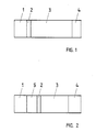
- Fig. 1 zeigt den Aufbau einer Einfach-Heterostruktur-IMPATT-Diode.
- Fig. 2 zeigt den Aufbau einer Doppel-Heterostruktur-IMPATT-Diode.
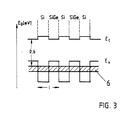
- Fig. 3 zeigt das Energiebandschema für ein Si/Si 0,2 Ge 0,8-Übergitter
- 1 shows the structure of a single heterostructure IMPATT diode.
- Fig. 2 shows the structure of a double heterostructure IMPATT diode.
- 3 shows the energy band diagram for a Si / Si 0.2 Ge 0.8 superlattice
Gemäß Fig. 1 ist auf einem p⁺-dotierten Si-Substrat 1 mit einer Ladungsträgerkonzentration von mehr als 10¹⁹ cm⁻³ eine Halbleiterschichtenfolge aus
- einer undotierten SiGe-Schicht 2 mit einer Schichtdicke von ungefähr 0,02 µm,
- einer n-dotierten Si-Schicht 3 mit einer Ladungsträgerkonzentration von ungefähr 1,4·10¹⁷ cm⁻³ und einer Schichtdicke von etwa 0,3 µm,
- einer n⁺-dotierten Si-Schicht mit einer Ladungsträgerkonzentration von ungefähr 5·10¹⁹ cm⁻³ und einer Schichtdicke von etwa 0,1 µm aufgebracht.1 is a semiconductor layer sequence on a p⁺-doped
an undoped
an n-doped
- An n⁺-doped Si layer with a charge carrier concentration of about 5 · 10¹⁹ cm⁻³ and a layer thickness of about 0.1 microns applied.
Die Bezeichnung "+" bedeutet starke Dotierung. Dotiermaterialien für die n-Dotierung sind z.B. Sb, P, As und für die p-Dotierung B, Ga, Al, In.The designation "+" means strong doping. Doping materials for the n-doping are, for example, Sb, P, As and for the p-doping B, Ga, Al, In.
An die Struktur gemäß Fig. 1 wird eine so hohe Sperrspannung angelegt, daß sich die Sperrschicht über die Halbleiterschichten 2, 3 erstreckt. An der Grenze zwischen p⁺-dotiertem Si-Substrat 1 und SiGe-Schicht 2 ist die maximale Feldstärke so groß, daß Stoßionisation einsetzt.A so high blocking voltage is applied to the structure according to FIG. 1 that the blocking layer extends over the
Der Halbleiterschichtaufbau einer IMPATT-Diode gemäß Fig. 1 unterscheidet sich von einer IMPATT-Diode auf Si-Basis mit p-n-Übergang dadurch, daß eine SiGe-Schicht 2 an der Stelle aufgewachsen ist, an der die zur Stoßionisation und damit die zur Lawinenmultiplikation erforderliche Feldstärke auftritt. Vorteilhafterweise besitzt SiGe einen kleineren Bandabstand Eg als Si (E g = 1,12eV) damit eine niedrigere Ionisationsschwellenenergie als Si. Für eine 0,0 2µm dicke Si 0,6Ge 0,4-Schicht beträgt der Bandabstand E g = 0,76eV.The semiconductor layer structure of an IMPATT diode according to FIG. 1 differs from an Si-based IMPATT diode with a pn junction in that an
Weiterhin wird durch die unterschiedlichen Gitterkonstanten von Si und SiGe eine laterale mechanische Spannung in den Halbleiterschichten erzeugt. Wird z.B. auf einem Si-Substrat 1 eine Si 0,6Ge 0,4-Schicht 2 mit einer unterkritischen Schichtdicke von etwa 0,02µm abgeschieden, so entsteht in der SiGe-Schicht eine laterale Druckspannung, da die natürliche Gitterkonstante von einkristallinem SiGe größer ist als die von einkristallinem Si. Eine Schichtdicke bezeichnet man als unterkritisch, wenn die aus verschiedenen Halbleitermaterialien bestehende Schichten in lateraler Richtung die gleiche Gitterkonstante besitzen. Es liegt dann ein pseudomorphes Wachstum vor. Die Druckspannung bewirkt eine Stauchung der SiGe-Schicht bis zu 4%. Die durch das pseudomorphe Wachstum entstandene mechanische Spannung führt zu einer Reduzierung des Band abstandes von SiGe und bewirkt eine zusätzliche Senkung der Ionisationsschwellenenergie von SiGe.Furthermore, the different lattice constants of Si and SiGe generate a lateral mechanical stress in the semiconductor layers. If, for example, an Si 0.6 Ge 0.4 layer 2 with a subcritical layer thickness of approximately 0.02 μm is deposited on an
Im Ausführungsbeispiel gemäß Fig. 2 ist eine IMPATT-Diode mit einer Doppel-Heterostruktur angegeben. Die Doppel-Heterostruktur unterscheidet sich beispielsweise von der Einfach-Heterostruktur (Fig.1) durch eine weitere p-dotierte Si-Schicht 5, die zwischen p⁺-dotiertem Substrat 1 und undotierter SiGe-Schicht 2 aufgewachsen ist (Fig. 2). Die Si-Schicht 5 besitzt eine Schichtdicke von ungefähr 0,25 µm und eine positive Ladungsträgerkonzentration von etwa 1,6 . 10¹⁷ cm⁻³. Das Substrat 1 und die Halbleiterschichten 2, 3, 4 sind bezüglich der Schichtdicke und Schichtzusammensetzung analog Ausführungsbeispiel 1 gewählt. Die durch die unterschiedliche Gitterkonstante von Si und SiGe verursachte mechanische Spannung in der SiGe-Schicht bewirkt vorteilhafterweise eine Verringerung des Bandabstandes in der SiGe-Schicht und eine Erniedrigung der Ionisationsschwellenenergie.In the exemplary embodiment according to FIG. 2, an IMPATT diode with a double heterostructure is specified. The double heterostructure differs, for example, from the single heterostructure (FIG. 1) in that it has a further p-doped
Die höhere Ionisationsrate von SiGe hat den Vorteil, daß der räumliche Bereich, in dem Verlustleistung auftritt, verkleinert wird und der Wirkungsgrad der IMPATT-Diode vergrößert wird. Der Wirkungsgrad der Heterostruktur-IMPATT-Dioden gemäß der Erfindung liegt für eine Frequenz von 100GHz zwischen 12 bis 15 %.The higher ionization rate of SiGe has the advantage that the spatial area in which power dissipation occurs is reduced and the efficiency of the IMPATT diode is increased. The efficiency of the heterostructure IMPATT diodes according to the invention is between 12 and 15% for a frequency of 100 GHz.
Zur Erhöhung des Wirkungsgrades der gattungsgemäßen IMPATT-Diode ist es außerdem vorteilhaft, die Generations zone als undotiertes Si/SiGe-Übergitter auszubilden. In einem Si/SiGe-Übergitter mit geeigneter Periodenlänge kann bei gleicher Schichtdicke wie für eine SiGe-Einzelschicht, der Ge-Anteil x in den Si 1-x Ge x-Schichten des Übergitters größer gewählt werden als in einer entsprechenden Si 1-xGe x-Einzelschicht. Durch die Erhöhung des Ge-Anteils x der Si 1-xGe x-Schichten und durch optimale Gestaltung der Periodenlänge des Si/SiGe-Übergitters läßt sich ein Miniband 6 im Energiebandschema des Si/SiGe-Übergitters (Fig. 3) erzeugen, dessen Bandabstand zum Leitungsband E c kleiner ist als der Bandabstand zwischen Valenz- und Leitungsband einer SiGe-Einzelschicht mit gleicher Schichtdicke. Beispielsweise betragen für eine Si 1-xGe x-Einzelschicht mit einer Schichtdicke von 0,02 µm der maximale Ge-Anteil x = 0,4 und der enstsprechende Bandabstand E g = 0,76eV. Für ein symmetrisches Si/Si 1-xGe x-Übergitter mit einer Schichtdicke von 0,02 µm, das aus einer Anzahl von fünf Perioden mit der Periodenlänge 1 = 0,004 µm aufgebaut ist, betragen der maximale Ge-Anteil x = 0,8 und der entsprechende Bandabstand E g = 0,6eV (Fig. 3). Bei einem symmetrischen Übergitter haben alle Einzelschichten des Übergitters die gleiche Schichtdicke.To increase the efficiency of the generic IMPATT diode, it is also advantageous for the generations zone as undoped Si / SiGe superlattice. In a Si / SiGe superlattice with a suitable period length, the Ge fraction x in the Si 1-x Ge x layers of the superlattice can be chosen larger than in a corresponding Si 1-x Ge with the same layer thickness as for a SiGe single layer x single layer. By increasing the Ge portion x of the Si 1-x Ge x layers and by optimally designing the period length of the Si / SiGe superlattice, a miniband 6 in the energy band diagram of the Si / SiGe superlattice (FIG. 3) can be generated, the Band gap to conduction band E c is smaller than the band distance between valence and conduction band of a SiGe single layer with the same layer thickness. For example, for a Si 1-x Ge x single layer with a layer thickness of 0.02 µm, the maximum Ge fraction x = 0.4 and the corresponding band gap E g = 0.76 eV. For a symmetrical Si / Si 1-x Ge x superlattice with a layer thickness of 0.02 µm, which is built up from a number of five periods with a period length of 1 = 0.004 µm, the maximum Ge fraction is x = 0.8 and the corresponding bandgap E g = 0.6 eV (Fig. 3). In the case of a symmetrical superlattice, all of the individual layers of the superlattice have the same layer thickness.
Die kritische Schichtdicke des Si/Si 1-xGe x-Übergitters ist bei gleichem Ge-Anteil x größer als bei einer Si 1-xGe x-Einzelschicht. Dadur ch kann die Schichtdicke der Generationszone bei Verwendung eines Si/SiGe-Übergitters größer gewählt werden als für eine SiGe-Einzelschicht. Das hat den Vorteil, daß die Übergitter-IMPATT-Diode über einen weiteren Frequenzbereich einsetzbar ist als die entsprechende Heterostruktur-IMPATT-Diode mit lediglich einer SiGe-Schicht.The critical layer thickness of the Si / Si 1-x Ge x superlattice is greater for the same Ge component x than for a Si 1-x Ge x single layer. As a result, the layer thickness of the generation zone can be selected to be larger when using an Si / SiGe superlattice than for an SiGe single layer. This has the advantage that the superlattice IMPATT diode can be used over a wider frequency range than the corresponding heterostructure IMPATT diode with only one SiGe layer.
Der Wellenlängenbereich der erfindungsgemäßen IMPATT-Dioden liegt im mm- und sub-mm-Bereich.The wavelength range of the IMPATT diodes according to the invention is in the mm and sub-mm range.
Die Heterostruktur-Halbeiterschichtenfolgen der erfindungsgemäßen IMPATT-Dioden wird mit dem Molekularstrahl-Epitaxie-Verfahren erzeugt.The heterostructure semiconductor layer sequences of the IMPATT diodes according to the invention are produced using the molecular beam epitaxy method.
Die Erfindung ist nicht auf die angegebene p⁺inn⁺- oder p⁺pinn⁺-Struktur der IMPATT-Dioden beschränkt, sondern sie ist auch auf die inversen Strukturen anwendbar, die dadurch entstehen, daß in den Ausführungsbeispielen der Leitungstyp der Halbleiterschichten vertauscht wird (n-Leitung wird durch p-Leitung ersetzt und umgekehrt). Weiterhin sind nicht nur die angegebenen Quasi-Read-Strukturen für die erfindungsgemäßen IMPATT-Dioden geeignet, sondern die Erfindung ist auch für Misawa-Dioden anwendbar. The invention is not limited to the specified p⁺inn⁺ or p⁺pinn⁺ structure of the IMPATT diodes, but can also be applied to the inverse structures which result from the fact that the conductivity type of the semiconductor layers is interchanged in the exemplary embodiments ( n line is replaced by p line and vice versa). Furthermore, not only the specified quasi-read structures are suitable for the IMPATT diodes according to the invention, but the invention can also be used for Misawa diodes.
Claims (7)
- einer undotierten SiGe-Schicht(2),
- einer n-dotierten Si-Schicht(3),
- einer n⁺-dotierten Si-Schicht(4) aufgewachsen ist.2. IMPATT diode according to claim 1, characterized in that on the p⁺-Si substrate (1) a heterostructure semiconductor layer sequence
- an undoped SiGe layer (2),
- an n-doped Si layer (3),
- An n⁺-doped Si layer (4) has grown.
dadurch gekennzeichnet, daß auf dem p⁺-Substrat (1) eine Heterostruktur-halbleiterschichtenfolge aus
- einer p-dotierten Si-Schicht(5),
- einer undotierten SiGe-Schicht(2),
- einer n-dotierten Si-Schicht(3),
- einer n⁺-dotierten Si-Schicht(4) aufgewachsen ist.3. IMPATT diode according to claim 1,
characterized in that a heterostructure semiconductor layer sequence is formed on the p⁺ substrate (1)
- a p-doped Si layer (5),
- an undoped SiGe layer (2),
- an n-doped Si layer (3),
- An n⁺-doped Si layer (4) has grown.
Applications Claiming Priority (4)
| Application Number | Priority Date | Filing Date | Title |
|---|---|---|---|
| DE3632921 | 1986-09-27 | ||
| DE3632921 | 1986-09-27 | ||
| DE3725214 | 1987-07-30 | ||
| DE19873725214 DE3725214A1 (en) | 1986-09-27 | 1987-07-30 | IMPATT DIODE |
Publications (2)
| Publication Number | Publication Date |
|---|---|
| EP0262346A1 true EP0262346A1 (en) | 1988-04-06 |
| EP0262346B1 EP0262346B1 (en) | 1993-03-31 |
Family
ID=25847918
Family Applications (1)
| Application Number | Title | Priority Date | Filing Date |
|---|---|---|---|
| EP87111422A Expired - Lifetime EP0262346B1 (en) | 1986-09-27 | 1987-08-07 | Impatt diode |
Country Status (3)
| Country | Link |
|---|---|
| US (1) | US4857972A (en) |
| EP (1) | EP0262346B1 (en) |
| DE (2) | DE3725214A1 (en) |
Cited By (2)
| Publication number | Priority date | Publication date | Assignee | Title |
|---|---|---|---|---|
| EP0593982A2 (en) * | 1992-10-20 | 1994-04-27 | Daimler-Benz Aktiengesellschaft | Si/SiGe BARITT-diode |
| WO2000025366A1 (en) * | 1998-10-23 | 2000-05-04 | The Secretary Of State For Defence | Improvements in impatt diodes |
Families Citing this family (12)
| Publication number | Priority date | Publication date | Assignee | Title |
|---|---|---|---|---|
| DE3937329B4 (en) * | 1989-11-09 | 2004-10-14 | Atmel Germany Gmbh | Semiconductor device and its use |
| US5168328A (en) * | 1990-07-03 | 1992-12-01 | Litton Systems, Inc. | Heterojunction impatt diode |
| US5466965A (en) * | 1992-12-02 | 1995-11-14 | The Regents Of The University Of California | High efficiency, high power multiquantum well IMPATT device with optical injection locking |
| DE4319211B4 (en) * | 1993-06-09 | 2004-04-15 | Daimlerchrysler Ag | Tunnel diode BARITT |
| US5685946A (en) * | 1993-08-11 | 1997-11-11 | The United States Of America As Represented By The Administrator Of The National Aeronautics And Space Administration | Method of producing buried porous silicon-geramanium layers in monocrystalline silicon lattices |
| US5550387A (en) * | 1994-01-24 | 1996-08-27 | Hi-Z Corporation | Superlattice quantum well material |
| DE19713962C1 (en) * | 1997-04-04 | 1998-07-02 | Siemens Ag | Power diode with charge coupling zones for freewheeling diode or voltage boundary controller |
| US6074960A (en) | 1997-08-20 | 2000-06-13 | Micron Technology, Inc. | Method and composition for selectively etching against cobalt silicide |
| DE19956903B4 (en) * | 1999-11-26 | 2009-04-09 | United Monolithic Semiconductors Gmbh | RF semiconductor device and method for integrating RF diodes |
| CN1309094C (en) * | 2004-03-17 | 2007-04-04 | 清华大学 | Hole resonance tunnel-through diode based on Si/SiGe |
| JP2013004541A (en) * | 2011-06-10 | 2013-01-07 | Toshiba Corp | Semiconductor storage device |
| US9412879B2 (en) | 2013-07-18 | 2016-08-09 | Texas Instruments Incorporated | Integration of the silicon IMPATT diode in an analog technology |
Citations (4)
| Publication number | Priority date | Publication date | Assignee | Title |
|---|---|---|---|---|
| US3466312A (en) * | 1964-06-08 | 1969-09-09 | Robins Co Inc A H | Derivatives of dialkyl-cysteines and allied compounds |
| FR2225842A1 (en) * | 1973-04-13 | 1974-11-08 | Thomson Csf | |
| US4291320A (en) * | 1980-01-10 | 1981-09-22 | Rockwell International Corporation | Heterojunction IMPATT diode |
| US4529455A (en) * | 1983-10-28 | 1985-07-16 | At&T Bell Laboratories | Method for epitaxially growing Gex Si1-x layers on Si utilizing molecular beam epitaxy |
Family Cites Families (3)
| Publication number | Priority date | Publication date | Assignee | Title |
|---|---|---|---|---|
| US3466512A (en) * | 1967-05-29 | 1969-09-09 | Bell Telephone Labor Inc | Impact avalanche transit time diodes with heterojunction structure |
| FR2379169A1 (en) * | 1977-01-28 | 1978-08-25 | Thomson Csf | AVALANCHE DIODE CONSTITUTED BY A HETERO-JUNCTION AND OSCILLATOR IN SO-CALLED "TRANSIT TIME" MODE INCLUDING SUCH A DIODE |
| US4257055A (en) * | 1979-07-26 | 1981-03-17 | University Of Illinois Foundation | Negative resistance heterojunction devices |
-
1987
- 1987-07-30 DE DE19873725214 patent/DE3725214A1/en not_active Withdrawn
- 1987-08-07 DE DE8787111422T patent/DE3785126D1/en not_active Expired - Fee Related
- 1987-08-07 EP EP87111422A patent/EP0262346B1/en not_active Expired - Lifetime
- 1987-09-28 US US07/105,952 patent/US4857972A/en not_active Expired - Lifetime
Patent Citations (4)
| Publication number | Priority date | Publication date | Assignee | Title |
|---|---|---|---|---|
| US3466312A (en) * | 1964-06-08 | 1969-09-09 | Robins Co Inc A H | Derivatives of dialkyl-cysteines and allied compounds |
| FR2225842A1 (en) * | 1973-04-13 | 1974-11-08 | Thomson Csf | |
| US4291320A (en) * | 1980-01-10 | 1981-09-22 | Rockwell International Corporation | Heterojunction IMPATT diode |
| US4529455A (en) * | 1983-10-28 | 1985-07-16 | At&T Bell Laboratories | Method for epitaxially growing Gex Si1-x layers on Si utilizing molecular beam epitaxy |
Non-Patent Citations (4)
| Title |
|---|
| APPLIED PHYSICS LETTERS, Band 47, Nr. 12, Dezember 1985, Seiten 1333-1335, Woodbury, New York, US; D.V. LANG et al.: "Measurement of the band gap of GexSi1-x/Si strained-layer heterostructures" * |
| PHYSICAL REVIEW B, Band 32, Nr. 2, 15. Juli 1985, Seiten 1405-1408, The American Physical Society, New York, US; R. PEOPLE: "Indirect band gap of coherently strained GexSi1-x bulk alloys on [001] silicon substrates" * |
| PROCEEDINGS OF THE IEEE, Band 61, Nr. 5, Mai 1973, Seiten 666-667, IEEE, New York, US; D.H. LEE: "Low-frequency noise of ion-implanted double-drift IMPATT diodes" * |
| SOLID STATE TECHNOLOGY, Band 28, Nr. 10, Oktober 1985, Seiten 137-143, Port Washington, New York, US; K.L. WANG: "Novel devices by Si-based molecular beam epitaxy" * |
Cited By (4)
| Publication number | Priority date | Publication date | Assignee | Title |
|---|---|---|---|---|
| EP0593982A2 (en) * | 1992-10-20 | 1994-04-27 | Daimler-Benz Aktiengesellschaft | Si/SiGe BARITT-diode |
| EP0593982A3 (en) * | 1992-10-20 | 1995-01-04 | Daimler Benz Ag | Si/SiGe BARITT-diode. |
| WO2000025366A1 (en) * | 1998-10-23 | 2000-05-04 | The Secretary Of State For Defence | Improvements in impatt diodes |
| US6774460B1 (en) | 1998-10-23 | 2004-08-10 | Qinetiq Limited | IMPATT diodes |
Also Published As
| Publication number | Publication date |
|---|---|
| DE3725214A1 (en) | 1988-03-31 |
| US4857972A (en) | 1989-08-15 |
| EP0262346B1 (en) | 1993-03-31 |
| DE3785126D1 (en) | 1993-05-06 |
Similar Documents
| Publication | Publication Date | Title |
|---|---|---|
| DE2801292A1 (en) | SEMICONDUCTOR COMPONENT WITH TWO-DIMENSIONAL CHARGE CARRIER FLOW | |
| EP0262346B1 (en) | Impatt diode | |
| EP0228516B1 (en) | Modulation-doped field-effect transistor | |
| DE69837030T2 (en) | SILICON-GERMANIUM SEMICONDUCTOR ASSEMBLY AND METHOD OF MANUFACTURING THEREOF | |
| EP1010204A1 (en) | Semiconductor structure comprising an alpha silicon carbide zone, and use of said semiconductor structure | |
| DE60131811T2 (en) | heterojunction bipolar transistor | |
| DE3136528A1 (en) | SEMICONDUCTOR AVALANCHE PHOTODETECTOR | |
| DE4025269A1 (en) | ELECTRONIC COMPONENT AND METHOD FOR THE PRODUCTION THEREOF | |
| DE2008043B2 (en) | Semiconductor oscillator element with superlattice | |
| DE112017002586B4 (en) | SILICON CARBIDE EPITAXIAL SUBSTRATE AND SILICON CARBIDE SEMICONDUCTOR COMPONENT | |
| DE1263934B (en) | Semiconductor component with three zones made of different semiconductor substances adjoining one another in the crystallographic [111] direction | |
| EP1770767B1 (en) | GaAs semiconductor substrate and semiconductor device | |
| EP0493706A1 (en) | Biaxial-stress barrier shifts in pseudomorphic tunnel devices | |
| EP0207266A2 (en) | Method of making a spatially periodic semiconductor multilayer structure | |
| DE2847451A1 (en) | Semiconductor drift transistor with different accelerations of charge - has tapered gap between valency band and conducting band in semiconductor zone | |
| EP0956626B1 (en) | Edge emitting semi-conductor laser component | |
| EP0681336A2 (en) | Electronic device with a semiconductor composite structure | |
| EP0593982B1 (en) | Si/SiGe BARITT-diode | |
| WO2002027802A1 (en) | Method for producing a body consisting of semiconductor material having a reduced mean free path length | |
| EP0697742B1 (en) | Quantum well optoelectronic device | |
| DE2356844C3 (en) | Electroluminescent semiconductor diode | |
| EP0634799B1 (en) | Transit time diode | |
| DE1154879B (en) | Method for generating a negative resistance in a semiconductor component | |
| DE10355949A1 (en) | Quantum Cascade Lasers | |
| DE102021000611A1 (en) | Stacked III-V semiconductor diode |
Legal Events
| Date | Code | Title | Description |
|---|---|---|---|
| PUAI | Public reference made under article 153(3) epc to a published international application that has entered the european phase |
Free format text: ORIGINAL CODE: 0009012 |
|
| AK | Designated contracting states |
Kind code of ref document: A1 Designated state(s): DE FR GB |
|
| 17P | Request for examination filed |
Effective date: 19880427 |
|
| 17Q | First examination report despatched |
Effective date: 19900817 |
|
| GRAA | (expected) grant |
Free format text: ORIGINAL CODE: 0009210 |
|
| AK | Designated contracting states |
Kind code of ref document: B1 Designated state(s): DE FR GB |
|
| REF | Corresponds to: |
Ref document number: 3785126 Country of ref document: DE Date of ref document: 19930506 |
|
| ET | Fr: translation filed | ||
| GBT | Gb: translation of ep patent filed (gb section 77(6)(a)/1977) |
Effective date: 19930708 |
|
| PLBE | No opposition filed within time limit |
Free format text: ORIGINAL CODE: 0009261 |
|
| STAA | Information on the status of an ep patent application or granted ep patent |
Free format text: STATUS: NO OPPOSITION FILED WITHIN TIME LIMIT |
|
| 26N | No opposition filed | ||
| REG | Reference to a national code |
Ref country code: GB Ref legal event code: 732E |
|
| REG | Reference to a national code |
Ref country code: FR Ref legal event code: TP |
|
| REG | Reference to a national code |
Ref country code: GB Ref legal event code: 732E |
|
| REG | Reference to a national code |
Ref country code: FR Ref legal event code: TP |
|
| REG | Reference to a national code |
Ref country code: GB Ref legal event code: IF02 |
|
| PGFP | Annual fee paid to national office [announced via postgrant information from national office to epo] |
Ref country code: GB Payment date: 20030728 Year of fee payment: 17 |
|
| PGFP | Annual fee paid to national office [announced via postgrant information from national office to epo] |
Ref country code: DE Payment date: 20030805 Year of fee payment: 17 |
|
| PGFP | Annual fee paid to national office [announced via postgrant information from national office to epo] |
Ref country code: FR Payment date: 20030813 Year of fee payment: 17 |
|
| PG25 | Lapsed in a contracting state [announced via postgrant information from national office to epo] |
Ref country code: GB Free format text: LAPSE BECAUSE OF NON-PAYMENT OF DUE FEES Effective date: 20040807 |
|
| PG25 | Lapsed in a contracting state [announced via postgrant information from national office to epo] |
Ref country code: DE Free format text: LAPSE BECAUSE OF NON-PAYMENT OF DUE FEES Effective date: 20050301 |
|
| GBPC | Gb: european patent ceased through non-payment of renewal fee |
Effective date: 20040807 |
|
| PG25 | Lapsed in a contracting state [announced via postgrant information from national office to epo] |
Ref country code: FR Free format text: LAPSE BECAUSE OF NON-PAYMENT OF DUE FEES Effective date: 20050429 |
|
| REG | Reference to a national code |
Ref country code: FR Ref legal event code: ST |