EP0275965A2 - Plasma operation apparatus - Google Patents
Plasma operation apparatus Download PDFInfo
- Publication number
- EP0275965A2 EP0275965A2 EP88100672A EP88100672A EP0275965A2 EP 0275965 A2 EP0275965 A2 EP 0275965A2 EP 88100672 A EP88100672 A EP 88100672A EP 88100672 A EP88100672 A EP 88100672A EP 0275965 A2 EP0275965 A2 EP 0275965A2
- Authority
- EP
- European Patent Office
- Prior art keywords
- magnetic field
- specimen
- plasma
- microwave
- discharge tube
- Prior art date
- Legal status (The legal status is an assumption and is not a legal conclusion. Google has not performed a legal analysis and makes no representation as to the accuracy of the status listed.)
- Granted
Links
Images


Classifications
-
- H—ELECTRICITY
- H05—ELECTRIC TECHNIQUES NOT OTHERWISE PROVIDED FOR
- H05H—PLASMA TECHNIQUE; PRODUCTION OF ACCELERATED ELECTRICALLY-CHARGED PARTICLES OR OF NEUTRONS; PRODUCTION OR ACCELERATION OF NEUTRAL MOLECULAR OR ATOMIC BEAMS
- H05H1/00—Generating plasma; Handling plasma
- H05H1/02—Arrangements for confining plasma by electric or magnetic fields; Arrangements for heating plasma
-
- H—ELECTRICITY
- H01—ELECTRIC ELEMENTS
- H01J—ELECTRIC DISCHARGE TUBES OR DISCHARGE LAMPS
- H01J37/00—Discharge tubes with provision for introducing objects or material to be exposed to the discharge, e.g. for the purpose of examination or processing thereof
- H01J37/32—Gas-filled discharge tubes
- H01J37/32009—Arrangements for generation of plasma specially adapted for examination or treatment of objects, e.g. plasma sources
- H01J37/32192—Microwave generated discharge
-
- C—CHEMISTRY; METALLURGY
- C23—COATING METALLIC MATERIAL; COATING MATERIAL WITH METALLIC MATERIAL; CHEMICAL SURFACE TREATMENT; DIFFUSION TREATMENT OF METALLIC MATERIAL; COATING BY VACUUM EVAPORATION, BY SPUTTERING, BY ION IMPLANTATION OR BY CHEMICAL VAPOUR DEPOSITION, IN GENERAL; INHIBITING CORROSION OF METALLIC MATERIAL OR INCRUSTATION IN GENERAL
- C23C—COATING METALLIC MATERIAL; COATING MATERIAL WITH METALLIC MATERIAL; SURFACE TREATMENT OF METALLIC MATERIAL BY DIFFUSION INTO THE SURFACE, BY CHEMICAL CONVERSION OR SUBSTITUTION; COATING BY VACUUM EVAPORATION, BY SPUTTERING, BY ION IMPLANTATION OR BY CHEMICAL VAPOUR DEPOSITION, IN GENERAL
- C23C16/00—Chemical coating by decomposition of gaseous compounds, without leaving reaction products of surface material in the coating, i.e. chemical vapour deposition [CVD] processes
- C23C16/44—Chemical coating by decomposition of gaseous compounds, without leaving reaction products of surface material in the coating, i.e. chemical vapour deposition [CVD] processes characterised by the method of coating
- C23C16/50—Chemical coating by decomposition of gaseous compounds, without leaving reaction products of surface material in the coating, i.e. chemical vapour deposition [CVD] processes characterised by the method of coating using electric discharges
- C23C16/511—Chemical coating by decomposition of gaseous compounds, without leaving reaction products of surface material in the coating, i.e. chemical vapour deposition [CVD] processes characterised by the method of coating using electric discharges using microwave discharges
-
- H—ELECTRICITY
- H01—ELECTRIC ELEMENTS
- H01J—ELECTRIC DISCHARGE TUBES OR DISCHARGE LAMPS
- H01J37/00—Discharge tubes with provision for introducing objects or material to be exposed to the discharge, e.g. for the purpose of examination or processing thereof
- H01J37/32—Gas-filled discharge tubes
- H01J37/32431—Constructional details of the reactor
- H01J37/3266—Magnetic control means
- H01J37/32678—Electron cyclotron resonance
Definitions
- This invention relates to plasma operation apparatus and more particularly to a plasma operation apparatus suitable for performing thin film deposition on a specimen (or substrate) surface or etching, sputtering or plasma oxidation for the specimen surface by utilizing plasma generated by microwave discharge.
- the plasma operation apparatus utilizing plasma generated by microwave discharge prevailing in a magnetic field has, within a discharge tube (also called. a. plasma generation chamber) forming a part of discharge space, a position at which electron cyclotron resonance (ECR) is caused by the magnetic field and a microwave and has a magnetic flux density distribution which decreases from the ECR conditioning position toward a specimen stand disposed within a specimen chamber. Consequently, plasma generated near the resonance position is decreased in density by an order of one to two or more during its transport from the discharge tube to the specimen stand and the plasma operation can not be done with high efficiency.
- ECR electron cyclotron resonance
- Fig. 1 illustrates an apparatus disclosed in "CVD utilizing ECR plasma", Transactions of 31st Semiconductor Integrated Circuit Technology Symposium held on December 3 and 4, 1986, pp. 49-54 and referred to as prior art example A hereinafter.
- prior art example A when a microwave 4 is introduced, through a wave guide 3 and an incident window 5, into a discharge tube 2 .surrounded by an external magnetic field coil 1 and the electron cyclotron motion in a magnetic field due to the magnetic coil 1 resonances with the microwave 4 at the resonance position, resonant electrons collide with and ionize a gas 6 for plasma, thus generating plasma.
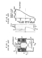
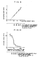
- Fig. 2 shows a magnetic flux density distribution occurring between the microwave incident window 5 and the specimen stand 8, where ordinate represents the distance in the direction of the central axis measured from the origin located at the boundary between discharge tube 2 and specimen chamber 9 and abscissa represents the magnetic flux density.
- the magnetic flux density Be effective to cause electron cyclotron resonance at a frequency of 2.45 GHz of the incident microwave 4 is 875 Gausses and Fig. 2 indicates that the resonance conditioning position is axially about 3 cm distant from the microwave incident window 5. Then, taking into account the characteristic of propagation of the microwave through the plasma and the resonance absorption condition for microwave energy, only a region inside the discharge tube 2 and which is within 3 cm distant from the microwave incident window 5 proves to be effective for plasma generation. Plasma generated in this region is transported over a distance of about 35 cm toward the specimen stand 8 under the influence of force due to the magnetic field divergence and of polarity diffusion.
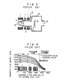
- Fig. 3 illustrates another apparatus disclosed in "Films of a - Si:H prepared by ECR plasma enhanced CVD", Transactions of 31 st Semiconductor Integrated Circuit Technology Symposium held on December 3 and 4, 1986, pp. 61-66 and referred to as prior art example B hereinafter, and Fig. 4 shows magnetic flux density distributions in the Fig. 3 apparatus.
- elements corresponding to those of Fig. 1 are designated by identical reference numerals.
- the level of the magnetic flux density distributions shown in Fig. 4 is higher as a whole. It will also be seen from Fig.
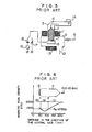
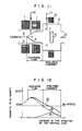
- Fig. 5 illustrates still another apparatus disclosed in J.P-A-59-3018 and referred to as a prior art example C hereinafter, and Fig. 6 shows a magnetic flux density distribution in the Fig. 5 apparatus.
- elements corresponding to those of Fig. 1 are designated by identical reference numerals.
- the prior art example C is directed to the configuration of the mirror magnetic field type frequently used in the plasma confinement method with the view of raising the plasma density and additionally has a complemental permanent magnet 13 for raising magnetic flux density near the surface of the specimen 7 housed in the specimen chamber 9.
- the incident microwave 4 propagates through a region designated at (I) in Fig.
- the plasma will be forced to direct toward the discharge tube owing to a magnetic field divergence appearing near the second resonance position, with the result that as in the case of prior art examples A and B, the density of plasma incident upon the specimen 7 tends to be smaller than that of the plasma near the first resonance position.
- JP-A-56-155535 Disclosed in JP-A-56-155535 is still another apparatus wherein, as in the prior art example A, a plasma activated species is generated in a plasma generation chamber and a plasma flux stemming from the activated species under the application of a divergent magnetic field is bombarded for operation upon a substrate to be operated which is sufficiently distant from a region of the maximal production efficiency of activated species.
- JP-A-57-79621 intends to improve efficiency and employs a magnet disposed externally of a substrate operation chamber and which restricts the radius of plasma flux to raise plasma density.
- a first object of this invention is to provide a plasma operation apparatus which can improve characters of films prepared by operation and can increase operation speeds by improving utilization efficiency of the generated plasma.
- a second object of this invention is to provide a plasma operation apparatus which can attain a highly efficient plasma operation by taking into account deactivation of a plasma activated species.
- a third object of this invention is to attain a highly efficient plasma operation which can attain excellent characters of performed films such as represented by densification, crystallinity and stoichiometry of deposited films.
- a first feature of this invention resides in that in a plasma operation apparatus, the magnetic flux density distribution starting from a plasma generation chamber (discharge tube) toward a specimen stand is so figured as to monotonously decrease, thereby providing a divergent magnetic field and that a position at which an ECR conditioning magnetic field is generated and the probability of generation of plasma is high is located at least partially within a specimen chamber to decrease the distance between the position at which high-density plasma is generated and a surface of a specimen.
- a second feature of this invention resides in that in a plasma operation apparatus, the divergent magnetic field is provided and that a substrate to be operated is distant by 150 mm at the maximum or less, preferably less than 70 mm, from an ECR position at which the generation of a plasma activated species is maximized.
- the distance between the ECR position and the substrate to be operated can be adjusted by increasing magnetic flux density within the plasma generation chamber or controlling the magnetic flux density with high accuracy.
- a third feature of this invention resides in that in a plasma operation apparatus, the divergent magnetic field is provided and that a range in which the magnitude of magnetic flux density is about 1.0 to 1.1 times that of magnetic flux density cooperating with the TE 01 mode (circular polarization) of a microwave to cause electron cyclotron resonance extends continuously in the direction of plasma flux over a distance of degree of the mean free path of an activated species, i.e., at least 50 mm or more or a distance range which requires the activated species to take a longer time than its mean life time to pass through the distance range.
- the range of the magnetic flux density having the above magnitude can be formed by disposing a plurality of divisional magnets aligned in the central axis direction of a vacuum system chamber or controlling the magnetic flux density with high accuracy.
- high-density plasma can be transported to the surface of the specimen to be operated and a thin film of high quality can be formed on the specimen surface within a short period of time. Further, operation efficiency dependent on film deposition rate and the like can be improved to improve throughput of manufacture process. In addition, even on the substrate to be operated at low temperatures, films having characters such as crystallinity and densification which are comparable to those of films prepared through an operation utilizing chemical reactions at high temperatures can be formed.
- a microwave propagating through a magnetic field to cause electron cyclotron resonance is of clockwise circular polarization and this microwave is cut off by a magnetic field having the magnitude of magnetic flux density smaller than that of magnetic flux density necessary for causing the electron cyclotron resonance and consequently can not propagate through the former magnetic field.
- the present invention takes advantage of this phenomenon and is constructed such that the magnitude of magnetic flux density at the incident edge of a discharge tube is made larger than that of magnetic flux density at the ECR position and the former magnetic flux density has a distribution which gradually decreases, starting from the discharge tube, toward a specimen stand, that a position at which the magnetic field and microwave cooperate together to cause the electron cyclotron resonance is located within a specimen chamber to provide a range which extends into the specimen chamber and in which the magnitude of magnetic flux density is larger than that of the resonance conditioning magnetic flux density to thereby generate high-density plasma, and that the distance over which plasma pushed out under the influence of a magnetic field divergence is transported to the specimen stand is minimized or zeroed in an extremity.
- the distance between resonance position and specimen stand can be minimized sufficiently, making it possible to transport high-density plasma to a surface of a specimen.
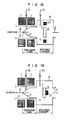
- a plasma operation apparatus according to a first embodiment of the invention which is relevant to the aforementioned first feature will be described with reference to Figs. 7, 8, 9 and 10.
- This embodiment of plasma operation apparatus is constructed as shown in Fig. 7 to perform a specimen surface operation (deposition) based on magnetic field/microwave discharge.
- a microwave 4 is introduced through a wave guide 3 into a discharge tube 2 surrounded by an external magnetic field coil 1 and a gas 6 for plasma is excited or ionized under the influence of electron cyclotron resonance caused by the electron cyclotron motion in a magnetic field due to the magnetic field coil 1 and the microwave 4, thereby generating plasma.
- the generated plasma is then pushed out into a specimen chamber 9 coupled to the discharge tube 2 and housing a specimen stand 8 for carrying or holding a specimen 7 to be operated.
- This plasma along with a material gas 10 additionally admitted toward the front of the specimen 7 inside the specimen chamber 9 and excited or ionized by the plasma flux, is transported to the surface of the specimen 7 so as to deposit a thin film having constituents of the plasma gas 6 and material gas 10 on the surface of the specimen 7.
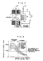
- Fig. 8 shows magnetic flux density distributions in the axis direction of the Fig. 7 apparatus between the discharge tube 2 and the specimen stand 8, where ordinate represents the distance in the axis direction and abscissa represents the magnetic flux density.
- the shape of distributions indicated by curves 0 and 2 is characteristic of this invention
- the shape of magnetic flux density distribution indicated by curve @ is obtained with an instance where the position of the ECR conditioning magnetic field is located at the boundary between. discharge tube 2 and specimen chamber 9, and an example of magnetic flux density distribution indicated by curve @ is for the aforementioned literature by S. Matsuo and K. Kiuchi.
- the microwave enters the specimen chamber 9 and approaches the resonance conditioning position, ionization and excitation become active under the influence of electron cyclotron resonance and in proportion thereto, the plasma density at the specimen position is increased, providing the plasma generation probability which is maximized at the resonance position.
- the microwave tending to pass through the high magnetic flux density region and propagate into a magnetic field having the magnetic flux density smaller than the resonance conditioning magnetic flux density (in this embodiment, 875 Gausses) is cut off and prevented from propagating, with the result that part of the microwave which has not been absorbed by resonance into the plasma is reflected at the resonance condition position. It therefore follows that almost no plasma generation takes place in the low magnetic flux density region which is offset from the resonance position toward the specimen stand 8.
- the resonance conditioning magnetic flux density in this embodiment, 875 Gausses
- the plasma reaching the surface of the specimen 7 contains plasma transported by polarity diffusion attendant on the magnetic field gradually decreasing, starting from the resonance position, toward the specimen stand 8 as well as atoms and molecules of the material gas 10 admitted near the resonance position and ionized and excited by the plasma flux. Accordingly, the plasma density distribution starting from the resonance position toward the specimen stand 8 exhibits an abrupt decrease.
- the distance between the resonance position and the specimen surface can be adjusted so as to be minimized or zeroed in an extremity, so that the specimen surface may be located to precede a position at which the plasma density begins to decrease abruptly.
- the operation rate substantially proportional to the electron density near the surface of the specimen 7, will not be decreased and besides the ion density contributing to ion bombardment affecting the densification of deposited films can be selected properly, thus ensuring that a thin film of high quality can be deposited within a short period of time.
- the magnitude of magnetic flux due to the magnetic field coil 1 of the present embodiment is so selected as to provide the resonance condition position which lies within the specimen chamber 9.
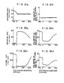
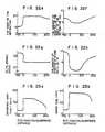
- Fig. 9 shows deposition rate for depositing thin films on the specimen surface with the apparatus of the present embodiment. Values are measured under the condition that film composition is constant.
- lower abscissa represents the shape of the magnetic flux density distribution in terms of curves 1 to 4 shown in Fig. 8
- upper abscissa represents, in arbitrary scale, electron density ratio on the specimen surface corresponding to the respective points 1 to 4, and ordinate represents deposition rate ratio in arbitrary scale.
- Fig. 9 clearly demonstrates that when the resonance position is located within the specimen chamber as indicated by points 1 and @ in Fig. 9, the electron density is increased to increase the deposition rate ratio, especially, in proportion to the degree of approaching of the resonance position to the surface of the specimen 7.
- Fig. 10 shows etching rate ratio representative of densification of thin films deposited on the specimen surface with the apparatus of the present embodiment, where lower abscissa represents the shape of the magnetic flux density distribution in terms of curves 1 to @ shown in Fig. 8, upper abscissa represents the magnetic flux density at the edge of discharge tube 2 which lies at the boundary between discharge tube 2 and specimen chamber 9, in terms of the magnitude of the magnetic flux density at the resonance condition position being Be and ordinate represents etching rate ratio in arbitrary scale.
- Fig. 10 clearly demonstrates that when the resonance position is drawn into the specimen chamber 9 as indicated by points 1 and @ in Fig. 10, the etching rate ratio is small proving that highly dense films are prepared and the plasma density near the specimen surface is high bringing about sufficient ion bombardment effect during film deposition.
- the high-density plasma can be generated near the specimen surface and highly dense thin films can be prepared at high deposition rates.
- FIG. 11 there is illustrated a plasma operation apparatus according to a second embodiment of the invention.
- this second embodiment of Fig. 11 additionally comprises a complemental magnetic field generation means 21, disposed externally of the specimen chamber 9, for generating within the specimen chamber 9 a magnetic field which aids in locating the position at which the ECR conditioning magnetic field is generated within the specimen chamber 9.
- Fig. 12 shows a magnetic flux density distribution in the axis direction of the Fig. 11 apparatus.
- broken-line curve @ indicates a magnetic flux density distribution obtained with only the magnetic field coil 1 shown in Fig. 11
- broken-line curve 0 indicates a magnetic flux density distribution obtained with only the complemental magnetic field generation means 21. Accordingly, in the apparatus of Fig.
- the curves @ and O 7 are superimposed together to provide a magnetic flux density distribution indicated by solid-line curve 5 in Fig. 12 by which the position of the ECR conditioning magnetic field is drawn in an arrow direction in Fig. 12 so as to be located within the specimen chamber 9.
- the complemental magnetic field generation means 21 is required to supply magnetic flux density of a magnitude of about 50 Gausses or more which is effective to locate the resonance condition position within the specimen chamber 9.
- the magnetic field coil 1 can be reduced in size to attain the same effect as that attained with the Fig.
- the position of the resonance conditioning magnetic field can be adjustably moved without greatly affecting the magnetic field distribution inside discharge tube 2 established by the magnetic field coil 1 and the radius and density of the plasma drawn by the complemental magnetic field generation means 21 can be controlled.
- Fig. 13 illustrates a plasma operation apparatus according to a third embodiment of the invention wherein the same complemental magnetic field generation means 21 as that used in the Fig. 11 embodiment is disposed externally of the specimen chamber 9 at a substantially intermediate position between discharge tube 2 and specimen chamber 9.
- Fig. 14 shows a magnetic flux density distribution in the axis direction of the Fig. 13 apparatus.
- a magnetic field due to the magnetic field coil as indicated by broken-line curve @ in Fig. 14 and a magnetic field due to the complemental magnetic field means 21 as indicated by broken-line curve @ in Fig. 14 are superimposed together to provide a magnetic flux density distribution as indicated by solid-line curve @ in Fig. 14.
- the third embodiment attains the same effect as that attained by the second embodiment of Fig. 11.
- a fourth embodiment of the invention comprises a complemental magnetic field generation means 21 disposed inside the specimen chamber 9 to attain the same effect as that by the foregoing embodiments.
- a fifth embodiment of the invention comprises a complemental magnetic field generation means 21 disposed at the back of the specimen stand 8 within the specimen chamber 9, attaining the same effect as that by the foregoing embodiments.
- a sixth embodiment of the invention comprises a complemental magnetic field generation means 21 playing the part of the specimen stand 8 within the specimen chamber 9 and serving as a specimen stand 8a with complemental magnetic field generation means.
- the sixth embodiment constructed as above can also attain the same effect as that by the foregoing embodiments.
- a seventh embodiment of the invention as illustrated in Fig. 18 acts as an etching apparatus.
- the gas 6 for plasma also serves as an etching gas. Since the position of the resonance conditioning magnetic field at which the probability of plasma generation is high can be controlled by means of the complemental magnetic field generation means 21 so as to be located within the specimen chamber 9, especially, between positions 0 and @ shown in Fig. 18, the proper etching condition can advantageously be set for the specimen 7 to be operated.
- the magnetic field has been described as having the shape of magnetic flux density distribution which substantially monotonously decreases starting from the discharge space into which the microwave is introduced toward the specimen stand but more briefly, the distribution may be so figured as to permit the resonance condition position to lie on a curved surface within the specimen chamber. In an alternative, the distance between the specimen and the resonance condition position may be lessened by moving the specimen stand.
- the pressure within the plasma generation chamber is not limited to 1 x 10 2 Torr or less in contrast to the prior art apparatus described in connection with Figs. 1 to 6.
- the magnetic flux density distribution is so figured as to monotonously decrease and the position of the ECR conditioning magnetic field at which the probability of plasma generation is high is located within the specimen chamber and besides the distance between the position for high-density plasma generation and the specimen surface is lessened, a very efficient plasma operation can be achieved wherein the high-density plasma can be transported to the specimen surface to prepare thin films of high quality at high operation speeds.
- the reaction gas is activated by microwave plasma discharge, especially, most efficiently activated near the ECR position.
- An.activated species thus created then loses its activity on account of energy dispersion or sometimes it is deactivated on account of inter-particle interaction due to its collision with other particles. Accordingly, a decreased distance between the substrate or specimen surface to be operated and the ECR position can permit the plasma activated species to reach the substrate while keeping activity of the plasma activated species high. This leads to a highly efficient plasma operation and inproved plasma operation characteristics.
- a deposited film advantageously approaches a film prepared by thermal chemical reaction.
- the activated species deposited on the substrate has a high probability of its reconfigurational and reorientational motion toward a molecular layer preexistent on the substrate until the energy of the activated species is minimized at a destination of the reconfigurational and reorientational motion. Therefore, the deposited film can be increased in densification and crystallinity. In addition, stoichiometric ratio of the deposited film approaches that of a film prepared by thermal chemical reaction.
- a plasma operation apparatus is - schematically illustrated in Fig. 19.
- the apparatus comprises a plasma generation chamber 104, a microwave guide 107 (an oscillator for a microwave is not illustrated), ECR magnetic field coils 109 and 113, an operation (specimen) chamber 102, an evacuation conduit 112 (an evacuation system is not illustrated), reaction gas supply nozzles 105 and 111 (a reaction gas supply system is not illustrated) and a substrate holder (specimen stand) 103.
- the plasma generation chamber 104 is made of colorless quartz and has a diameter of 240 mm and a length of 250 mm with its top cone serving as a microwave incident window 108.
- the ECR magnetic field coils 109 and 113 respectively surround the plasma generation chamber and the operation chamber and are operable to provide a maximum of magnetic flux density of 2.6 K Gausses within the plasma generation chamber.
- the coils 109 and 113 are respectively divided into three and two sub-coils which can be adjusted separately to control the magnetic flux density.
- the operation chamber 102 is made of stainless and has a diameter of 240 mm.
- the substrate holder 103 having a diameter of 120 mm and placed in the operation chamber is made of alumina and its position is variable along the direction of plasma flux (in the right and left directions in the drawing).
- Fig. 20 graphically exemplifies magnetic flux density distributions in the direction of microwave propagation.
- Various distributions (D to mO can be established by adjusting the ECR magnetic field coils 109 and 113, and the distance between the substrate and the ECR position can be controlled by adjustably setting the position of the substrate holder 103.
- a silicon wafer having a diameter of 100 mm is used and a silicon oxide film is formed on the wafer.
- Oxygen is admitted at a flow rate of 40 ml/min into the plasma generation chamber 104 through the first gas inlet pipe 105 and a microwave 106 of 2.45 GHz propagating through the wave guide 107 is introduced into the plasma generation chamber 104 through the microwave incident window 108.
- a magnetic field of 875 Gausses or more is generated from the static magnetic field generation coils 109 and 113 both disposed externally of and concentrically with the plasma generation chamber to generate a plasma flux 110 and monosilane (SiH 4 ) is admitted at a flow rate of 6 ml/min through the second gas inlet pipe 111 into the operation chamber 102 which is evaculated by the evaculation system to a reduced pressure of 1 m Torr.
- the magnetic flux density distribution is controlled by adjusting the amount of currents passed through the static magnetic field generation coils 109 and 113 or the distance between the ECR position and the substrate to be operated is adjustably changed by adjusting the position of the substrate holder.
- the Si0 2 film deposition rate and the amount of scatter of the deposition rate within the substrate are graphically depicted in Figs. 21 a and 21 b
- the etching rate for the deposited film under etching with a buffer etching solution (a mixture of 1-mol HF and 6-mol NH 4 F) and the amount of scatter of the etching rate within the substrate are graphically depicted in Figs. 21 and 21 d
- the index of refraction of the deposited film and the amount of scatter of the index of refraction within the substrate are graphically depicted in Figs. 21 and 21f
- Figs. 21 g and 21 h deposited film measured through Auger electron spectroscopy and the amount of scatter of the Si/O atomic ratio within the substrate are graphically depicted in Figs. 21 g and 21 h.
- broken-line curves are representative of results obtained when the substrate is positioned within the plasma generation chamber.
- Fig. 21 demonstrates that the amount of scatter of the deposition rate is small within the range of distance d of from 0 to 70 mm, indicating excellent uniformity.
- Fig. 21 demonstrates that the amount of scatter of the deposition rate is small within the range of distance d of from 0 to 70 mm, indicating
- Fig. 21c demonstrates that the etching rate is low within the range covering a distance d of 150 mm or less, indicating that films of high densification can be prepared within this range and Fig. 21d demonstrates that excellent uniformity can be obtained within the range of distance d of from 0 to 70 mm.
- Fig. 21 e demonstrates that the deposited film has the index of refraction approximating that of a film prepared by thermal oxidation within the range of distance d of from 0 to 150 mm and Fig. 21 f demonstrates that excellent uniformity can be obtained within the range of distance d of from 0 to 70 mm.
- Fig. 21 g demonstrates that the SiiO atomic ratio is 0.5 within the range covering a distance d of 0 (zero) or more and Fig. 21 h demonstrates that uniformity is excellent.
- the characteristic of the film deposition by microwave plasma discharge greatly depends on the maximum generation region for the plasma activated species, that is, the distance between the ECR position and the substrate in the apparatus. Further, it should be understood that the desirable value of distance d free from the influence of the deactivation of activated species due to its life and interaction such as collision with inactive molecules is below the mean free path of the activated species. Furthermore, it has been proved that within the range of distance d of from 0 to 70 mm, uniformity of performed films and film quality is excellent and this range coincides with the range of deactivation time of such an activated species as SiH 2 of monosilane. In the latter range, the range of deactivation time corresponds to the range of lifetime within which the activated species makes a transition from a highly excited state to the ground state of zero electron energy.
- a nitrogen gas is admitted at a flow rate of 40 ml/min to the plasma generation chamber through the first gas inlet pipe
- a monosilane (SiHa) gas is admitted at a flow rate of 6 ml/min to the operation chamber through the second gas inlet pipe
- a SbN4 film is deposited inside the operation chamber which is evacuated to a pressure of 1 m Torr.
- Results are graphically illustrated in Figs. 22a to 22h. As in the case of the Si0 2 film deposition described with reference to Figs.
- the deposition rate, etching rate for the film, index of refraction, stoichiometric ratio and their amounts of scatter within the substrate greatly depend on the distance d between the ECR position and the substrate.
- the stoichiometric ratio Si/N mol ratio
- the stoichiometric ratio is constant and within the range of distance d of from 0 to 150 mm, the etching rate for the deposited film and the index of refraction thereof equalling or approximating those of a thermal nitrogenated film can be obtained and the deposition rate is high.
- uniformity of the deposited film within the substrate is relatively high as in the case of the Si0 2 deposited film.
- a hydrogen gas is admitted to the plasma generation chamber through the first gas inlet pipe, a monosilane (SiHa) gas is admitted to the operation chamber through the second gas inlet pipe, and a polycrystalline silicon film is deposited inside the operation chamber by maintaining the substrate at a temperature of 320°C.
- Results are graphically illustrated in Figs. 23a and 23b. It will be seen from these Figures that within the range of distance d of from 0 to 150 mm, the deposition rate is high and the crystal grain size of the polycrystalline silicon examined through X-ray diffraction is high, exhibiting excellent crystallinity.
- a hydrogen gas is admitted through the first gas inlet pipe, a tungsten hexafluoride (WF 6 ) gas is admitted through the second gas inlet pipe, and a tungsten film is deposited inside the operation chamber which is at a reduced pressure of 0.3 m Torr.
- WF 6 tungsten hexafluoride
- a low-resistance film having a resistivity of 4.0 ⁇ /cm approximating that of a bulk resistor can be deposited efficiently.
- a WF 6 activated species has, in its life, a mean free path approximating that of a SiH 4 activated species and the character of the deposited film proves to be excellent within the range of deactivation time.
- a mixture gas of hydrogen and nitrogen is admitted through the first gas inlet pipe, trichloro aluminum (AtCt 3 ) carried by a N 2 carrier is admitted through the second gas inlet pipe, and Aluminum nitride is deposited inside the operation chamber.
- Measurement results of deposition rate and breakdown voltage of the deposited film are graphically depicted in Figs. 25a and 25b. Within the range of distance d of from 0 to 150 mm, an excellent insulator having a breakdown voltage of 5 MV/cm or more can be prepared efficiently. The surface state density of this deposited film is excellent, measuring 10 10 cm 2 .
- a sulfur hexafluoride (SF 6 ) gas is admitted through the first gas inlet pipe so as to etch polycrystalline silicon.
- Measurement results of etching rate for the polycrystalline silicon and etching selective ratio (Si/Si0 2 ) are graphically depicted in Figs. 26a and 26b.
- the polycrystalline silicon can be etched highly selectively and efficiently.
- the previous eighth to thirteenth embodiments show that the microwave operation efficiency and the character of deposited films greatly depend on the distance d between the ECR position and the substrate to be operated, that is, the life of plasma activated species and the deactivated degree of electron energy of the activated species due to interaction such as collision with inactive species or the decreasing degree of vibration, rotation and translation energy and as a result, the excellent deposition rate and film quality can be obtained within the range of distance d of from 0 to 150 mm. Particularly, under the influence of distributions of the life of plasma activated species and of the deactivated degree, uniformity of the deposition rate and film quality can be high within the range of distance d of from 0 to 70 mm.
- the distance between the ECR position and the substrate is made less than 150 mm, thereby ensuring that in the microwave plasma operation, the film deposition rate can be improved to realize a consequent improvement in throughput and that films having crystallinity and densification comparable to those of films prepared by high temperature chemical reaction can be deposited on the operated substrate which is even at low temperatures.
- the angular frequency of a microwave applied is ⁇
- the magnetic flux density of a static magnetic field is B and the mass of electron is m e
- Z is a coordinate position on a vacuum-chamber-center-axis coordinate system which is positive in the direction of plasma flux
- r is the radius of rotational motion of the electron
- e is the electric charge of the electron.
- the ECR surface is, in effect, expanded into an effective ECR range having an ECR efficiency distribution in the direction of propagation.
- a high generation efficiency range of plasma activated species is set up having a distribution similar to the ECR efficiency distribution. Accordingly, if the high generation efficiency range can be enlarged, the concentration of plasma activated species can be increased and consequently the operation efficiency for the operated object can be increased.
- the higher the concentration of the deposited activated species having the high kinetic energy the more the densification and crystallinity of the deposited film can be improved.
- stoichiometric ratio of the deposited film approaches that of a film prepared by thermal chemical reaction.
- the degree of deactivation of the plasma activated species due to inter-molecule interaction such as based on collision can be decreased and therefore it is expected that the operation can be performed more efficiently and properly.
- the microwave is prevented from propagating at a position satisfying dB/dZ > 0 and the production efficiency of the plasma activated species is disadvantageously degraded.
- the essential part of a plasma operation apparatus is schematically illustrated in Fig. 27.
- the apparatus comprises a plasma generation chamber 204, a microwave guide 207 (an oscillator for a microwave 206 is not illustrated), ECR magnetic field coils 209 and 213, an operation chamber 202, an evacuation conduit 212 (an evacuation system is not illustrated), reaction gas supply nozzles 205 and 211 (a reaction gas supply system is not illustrated), and a substrate holder 203.
- the plasma generation chamber 204 is made of colorless quartz and has a diameter of 240 mm and a length of 250 mm with its top cone serving as a microwave incident window 208.
- the ECR magnetic field coifs 209 and 213 respectively surround the plasma generation chamber and the operation chamber and are operable to provide a maximum of magnetic field density of 3.0 K Gausses within the plasma generation chamber.
- the ECR magnetic field coils 209 and 213 are respectively divided into five and three sub-coils. Magnitude and direction of currents supplied to these sub-coils can be adjusted separately to control the magnetic flux density.
- the operation chamber 202 is made of stainless and has a diameter of 240 mm.
- the substrate holder 203 having a diameter of 120 mm and placed in the operation chamber is made of alumina and its position is variable along the direction of plasma flux (in the right and left directions in the drawing).
- Fig. 28a and 28b graphically illustrate magnetic flux density distributions represented by B (Z), where Z is a coordinate position on a vacuum-chamber-center-axis coordinate system which is positive in the direction of plasma flux and has the origin at the substrate in the case of Fig. 28a and at the edge of the plasma generation chamber in the case of Fig. 28b.
- Z is a coordinate position on a vacuum-chamber-center-axis coordinate system which is positive in the direction of plasma flux and has the origin at the substrate in the case of Fig. 28a and at the edge of the plasma generation chamber in the case of Fig. 28b.
- FIG. 28a shows examples of magnetic field distributions established when a distribution of predetermined shape is changed by changing the intensity. of magnetic field at a uniform rate and Fig. 28b shows examples of magnetic field distributions established when a distribution obtained for substantially constant B/B e measuring about 1.1 is changed by changing the distance between the ECR position and the substrate.
- a silicon wafer having a diameter of 100 mm is used and a silicon oxide film is formed on the wafer.
- Oxygen (0 2 ) is admitted at a flow rate of 40 ml/min into the plasma generation chamber 204 through the first gas inlet pipe 205, a microwave 206 of 2.45 GHZ is introduced into the plasma generation chamber, a magnetic field of 875 Gausses or more is generated from the static magnetic field generation coils 209 and 213 to generate a plasma flux 210, monosilane (SiH 4 ) is admitted at a flow rate of 6 ml/min through the second gas inlet pipe 211 into the operation chamber 202 which is evacuated by the evacuation system to a reduced pressure of 1 m Torr.
- the magnetic flux density distribution is controlled by adjusting the amount of currents passed through the static magnetic field generation coils 209 and 213.
- a Si0 2 film is deposited by raising, as shown in Fig. 28a, the magnitude of magnetic flux density so as to change of ECR range while keeping constant the distance between the substrate and the ECR position or by decreasing, as shown in Fig. 28b, the distance between the substrate and the ECR position while keeping the magnitude of magnetic flux density substantially constant.
- Fig. 29a graphically depicts dependency of the Si0 2 deposition rate upon the magnetic flux density affecting the effective ECR range
- Fig. 29b graphically depicts dependency of the deposition rate upon the length of the effective ECR range. In Figs. 29a and 29b, errors are maximum errors for the same substrate.
- FIG. 29c graphically depicts dependency of the etching rate for the deposited film under etching with a buffer etching solution (a mixture of 1-mol HF and 6-mol NH 4 F) upon the magnetic flux density for the effective ECR range
- Fig. 29d depicts dependency of the etching rate upon the length of the effective ECR range
- Fig. 29e depicts dependency of the optical index of refraction of the deposited film upon the magnetic flux density
- Fig. 29f depicts dependency of the index of refraction upon the length
- Fig. 29g depicts dependency of the Si/0 mol ratio in the deposited film measured through Auger electron spectroscopy upon the magnetic flux density
- Fig. 29h depicts dependency of the Si/0 mol ratio upon the length.
- the value of B/B o is measured for the distance between the ECR position and the substrate being 100 mm
- the distance At is measured for B/B o ⁇ 1.0 to 1.1.
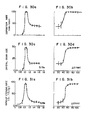
- Figs. 29a and 29b demonstrate that the deposition rate is highly efficient for the B/B o being 1.0 to 1.1 and for the At being 50 mm or more.
- Figs. 29c and 29d demonstrate that the etching rate is low also for the B/B o being 1.0 to 1.1 and for the At being 50 mm or more, indicating that the deposited film proves to be of high densification.
- Figs. 29e, 29f, 29g and 29h demonstrate that for the B/B o being 1.0 to 1.1 and the At being 50 mm or more, a deposited film comparable to a thermally oxygenated film can be prepared. It is therefore concluded that there exists the effective ECR range in the microwave plasma operation and that highly efficient operations and high-quality deposited films can be obtained by enlarging the effective ECR range.
- Figs. 30a and 30b graphically depict results, indicating that the deposition rate is high for the B/B e being 1.0 to 1.1 and the At being 50 mm or more. Examination based on X-ray diffraction has proven that the polycrystalline silicon prepared under the above conditions has a large grain size as shown in Figs. 30c and 30d, exhibiting excellent crystallinity.
- Figs. 31a and 31 b show results, indicating that, as in the case of the fourteenth and fifteenth embodiments, for the B/B e being 1.0 to 1.1 and the At being 50 mm or more, selective etching for polycrystalline silicon material which is required for etching LSI gate materials can be performed.
- the microwave plasma operation efficiency and operation characteristics greatly depend upon breadth of the effective ECR range. Accordingly, the concentration of the plasma activated species can be increased by enlarging the effective ECR range to improve efficiency of plasma operations and the quality of deposited films or etching characteristic therefor can be made excellent by maintaining the high energy state of the activated species for a long period of time, thereby optimizing the plasma operation.
- the above advantages can be attained by establishing the continuous range in which the magnitude of magnetic flux density is 1.0 to 1.1 times the magnitude of magnetic flux density necessary for the theoretical ECR condition in the TE o1 mode of the microwave and by setting the length of that range to be 50 mm or more.
- the film deposition rate and operation efficiency can be improved in the microwave plasma operation and consequently the throughput of manufacture process can be improved. Further, in film deposition, films having crystallinity and densification comparable to those of films prepared by high temperature chemical reaction can be deposited on the operated substrate which is even at low temperatures.
Abstract
Description
- This invention relates to plasma operation apparatus and more particularly to a plasma operation apparatus suitable for performing thin film deposition on a specimen (or substrate) surface or etching, sputtering or plasma oxidation for the specimen surface by utilizing plasma generated by microwave discharge.
- The plasma operation apparatus utilizing plasma generated by microwave discharge prevailing in a magnetic field has, within a discharge tube (also called. a. plasma generation chamber) forming a part of discharge space, a position at which electron cyclotron resonance (ECR) is caused by the magnetic field and a microwave and has a magnetic flux density distribution which decreases from the ECR conditioning position toward a specimen stand disposed within a specimen chamber. Consequently, plasma generated near the resonance position is decreased in density by an order of one to two or more during its transport from the discharge tube to the specimen stand and the plasma operation can not be done with high efficiency.
- Fig. 1 illustrates an apparatus disclosed in "CVD utilizing ECR plasma", Transactions of 31st Semiconductor Integrated Circuit Technology Symposium held on December 3 and 4, 1986, pp. 49-54 and referred to as prior art example A hereinafter. In the prior art example A, when a
microwave 4 is introduced, through awave guide 3 and anincident window 5, into adischarge tube 2 .surrounded by an external magnetic field coil 1 and the electron cyclotron motion in a magnetic field due to the magnetic coil 1 resonances with themicrowave 4 at the resonance position, resonant electrons collide with and ionize a gas 6 for plasma, thus generating plasma. Under the influence of a magnetic field divergence, the generated plasma is then pushed out into aspecimen chamber 9 coupled to thedischarge tube 2 and housing aspecimen stand 8 for carrying or holding aspecimen 7. This plasma alone or along with atoms or molecules of amaterial gas 10 additionally introduced into thespecimen chamber 9 and excited or ionized by that plasma is used for plasma operation of a surface of thespecimen 7. Fig. 2 shows a magnetic flux density distribution occurring between themicrowave incident window 5 and thespecimen stand 8, where ordinate represents the distance in the direction of the central axis measured from the origin located at the boundary betweendischarge tube 2 andspecimen chamber 9 and abscissa represents the magnetic flux density. In the case of this prior art example A, the magnetic flux density Be effective to cause electron cyclotron resonance at a frequency of 2.45 GHz of theincident microwave 4 is 875 Gausses and Fig. 2 indicates that the resonance conditioning position is axially about 3 cm distant from themicrowave incident window 5. Then, taking into account the characteristic of propagation of the microwave through the plasma and the resonance absorption condition for microwave energy, only a region inside thedischarge tube 2 and which is within 3 cm distant from themicrowave incident window 5 proves to be effective for plasma generation. Plasma generated in this region is transported over a distance of about 35 cm toward thespecimen stand 8 under the influence of force due to the magnetic field divergence and of polarity diffusion. In this transport, the long transport distance and an abrupt decrease in the magnetic field (magnetic flux density) cause a loss and because of this loss, the density of plasma reaching the surface of thespecimen 7 through transport tends to be smaller than that of plasma near the resonance position at which the electron cyclotron resonance occurs. - Fig. 3 illustrates another apparatus disclosed in "Films of a - Si:H prepared by ECR plasma enhanced CVD", Transactions of 31 st Semiconductor Integrated Circuit Technology Symposium held on December 3 and 4, 1986, pp. 61-66 and referred to as prior art example B hereinafter, and Fig. 4 shows magnetic flux density distributions in the Fig. 3 apparatus. In Fig. 3, elements corresponding to those of Fig. 1 are designated by identical reference numerals. When compared to the magnetic flux density distribution of the prior art example A, the level of the magnetic flux density distributions shown in Fig. 4 is higher as a whole. It will also be seen from Fig. 4 that the position for 875-Gauss magnetic flux density corresponding to the ECR position still lies within the
discharge tube 2 and magnetic flux density exceeding 875 Gausses also prevails within thedischarge tube 2, indicating that a region effective for the resonance absorption of microwave measures about 2/3 of thedischarge tube 2 at its maximum. In addition, the magnetic flux density is abruptly decreased toward thespecimen stand 8. Consequently, as in the case of prior art example A, the density of plasma generated near the resonance position tends to suffer from a loss and decrease during diffusion of the plasma toward the surface of thespecimen 7. - Fig. 5 illustrates still another apparatus disclosed in J.P-A-59-3018 and referred to as a prior art example C hereinafter, and Fig. 6 shows a magnetic flux density distribution in the Fig. 5 apparatus. In Fig. 5, elements corresponding to those of Fig. 1 are designated by identical reference numerals. The prior art example C is directed to the configuration of the mirror magnetic field type frequently used in the plasma confinement method with the view of raising the plasma density and additionally has a complemental
permanent magnet 13 for raising magnetic flux density near the surface of thespecimen 7 housed in thespecimen chamber 9. In this prior art example C, theincident microwave 4 propagates through a region designated at (I) in Fig. 6 in which the magnetic flux density is higher than that at the resonance position, and themicrowave 4 then undergoes res- onarice absorption by the plasma near a first resonance position designated at s in Fig. 6. And, it is difficult for the microwave reaching the first resonance position to pass therethrough and propagate into a smaller 'magnetic flux density region designated at (II) in Fig. 6 because this tendency of the microwave is resisted by the plasma. If the propagation leaks for approaching a second resonance position designated at t in Fig. 6 which is near thespecimen 7 on thespecimen stand 8 and plasma is generated at the second resonance position, the plasma will be forced to direct toward the discharge tube owing to a magnetic field divergence appearing near the second resonance position, with the result that as in the case of prior art examples A and B, the density of plasma incident upon thespecimen 7 tends to be smaller than that of the plasma near the first resonance position. - Disclosed in JP-A-56-155535 is still another apparatus wherein, as in the prior art example A, a plasma activated species is generated in a plasma generation chamber and a plasma flux stemming from the activated species under the application of a divergent magnetic field is bombarded for operation upon a substrate to be operated which is sufficiently distant from a region of the maximal production efficiency of activated species.
- Further a known plasma operation method as disclosed in JP-A-57-79621 intends to improve efficiency and employs a magnet disposed externally of a substrate operation chamber and which restricts the radius of plasma flux to raise plasma density.
- All of the prior arts described hereinbefore do not thoroughly consider the problem that the density of plasma generated by the microwave subject to the electron cyclotron resonance in the magnetic field suffers from a loss during transport of the plasma to the specimen surface, that is, the problem concerning life of the plasma activated species or deactivation thereof during transport of the plasma activated species until the substrate to be operated, and they can not always succeed in improving efficiency of the plasma operation. Also, with the prior arts, excellent characters of the performed films such as represented by densification, crystallinity and stoichiometry of the deposited films can not be obtained.
- Another literature relevant to the present invention is "Low Temperature Chemical Deposition Method Utilizing an Electron Cyclotron Resonance Plasma" by S. Matsuo and K. Kiuchi, Jpn. J. Appl. Phys. 22(4), L210, 1983.
- A first object of this invention is to provide a plasma operation apparatus which can improve characters of films prepared by operation and can increase operation speeds by improving utilization efficiency of the generated plasma.
- A second object of this invention is to provide a plasma operation apparatus which can attain a highly efficient plasma operation by taking into account deactivation of a plasma activated species.
- A third object of this invention is to attain a highly efficient plasma operation which can attain excellent characters of performed films such as represented by densification, crystallinity and stoichiometry of deposited films.
- A first feature of this invention resides in that in a plasma operation apparatus, the magnetic flux density distribution starting from a plasma generation chamber (discharge tube) toward a specimen stand is so figured as to monotonously decrease, thereby providing a divergent magnetic field and that a position at which an ECR conditioning magnetic field is generated and the probability of generation of plasma is high is located at least partially within a specimen chamber to decrease the distance between the position at which high-density plasma is generated and a surface of a specimen.
- A second feature of this invention resides in that in a plasma operation apparatus, the divergent magnetic field is provided and that a substrate to be operated is distant by 150 mm at the maximum or less, preferably less than 70 mm, from an ECR position at which the generation of a plasma activated species is maximized. The distance between the ECR position and the substrate to be operated can be adjusted by increasing magnetic flux density within the plasma generation chamber or controlling the magnetic flux density with high accuracy.
- A third feature of this invention resides in that in a plasma operation apparatus, the divergent magnetic field is provided and that a range in which the magnitude of magnetic flux density is about 1.0 to 1.1 times that of magnetic flux density cooperating with the TE01 mode (circular polarization) of a microwave to cause electron cyclotron resonance extends continuously in the direction of plasma flux over a distance of degree of the mean free path of an activated species, i.e., at least 50 mm or more or a distance range which requires the activated species to take a longer time than its mean life time to pass through the distance range. The range of the magnetic flux density having the above magnitude can be formed by disposing a plurality of divisional magnets aligned in the central axis direction of a vacuum system chamber or controlling the magnetic flux density with high accuracy.
- According to the invention, high-density plasma can be transported to the surface of the specimen to be operated and a thin film of high quality can be formed on the specimen surface within a short period of time. Further, operation efficiency dependent on film deposition rate and the like can be improved to improve throughput of manufacture process. In addition, even on the substrate to be operated at low temperatures, films having characters such as crystallinity and densification which are comparable to those of films prepared through an operation utilizing chemical reactions at high temperatures can be formed.
- Other objects and features of the present invention will become apparent from the reading of the following description.
-
- Figure 1 is a fragmentary sectional view illustrating a plasma operation apparatus according to the first prior art example.
- Figure 2 is a diagram showing a magnetic flux density distribution in the central axis direction in the apparatus of Fig. 1.
- Figure 3 is a fragmentary sectional view illustrating a plasma operation apparatus according to the second prior art example.
- Figure 4 is a graphic representation showing magnetic flux density distributions in the central axis direction in the Fig. 3 apparatus.
- Figure 5 is a schematic diagram illustrating a plasma operation apparatus according to the third prior art example.
- Figure 6 is a graphic representation showing a magnetic flux density distribution in the central axis direction in the Fig. 5 apparatus.
- Figure 7 is a schematic diagram illustrating a plasma operation system according to a first embodiment of the invention.
- Figure 8 is a graph showing magnetic flux density distributions in the axis direction in the Fig. 7 apparatus.
- Figure 9 is a graph showing the relation of deposition rate ratio obtained during deposition with the Fig. 7 apparatus with respect to the shape of the magnetic flux distributions and the electron density ratio related thereto.
- Figure 10 is a graph showing the relation between etching rate ratio for deposited thin films obtained with the Fig. 7 apparatus and magnetic flux density.
- Figure 11 is a shematic diagram illustrating a plasma operation system according to a second embodiment of the invention.
- Figure 12 is a graph showing a magnetic flux density distribution in the Fig. 11 apparatus.
- Figure 13 is a schematic diagram illustrating a plasma 'operation system according to a third embodiment of the invention.
- Figure 14 is a graph showing a magnetic flux density distribution in the apparatus of Fig. 13.
- Figure 15 is a schematic diagram illustrating a plasma operation system according to a fourth embodiment of the invention.
- Figure 16 is a similar diagram of a fifth embodiment of the invention.
- Figure 17 is a similar diagram of a sixth embodiment of the invention.
- . Figure 18 is a similar diagram of a seventh embodiment of the invention.
- Figure 19 is a similar diagram of an eighth embodiment of the invention.
- Figure 20 is a graph showing magnetic flux density distributions in the axis direction in the Fig. 19 apparatus.
- Figures 21 a to 21 h are graphs showing various experimental data obtained with the Fig. 19 apparatus to prove characteristics thereof.
- Figures 22a to 22h are graphs showing other experimental data obtained with the Fig. 19 apparatus.
- Figures 23a and 23b, 24a and 24b, 25a and 25b and 26a and 26b are graphs showing further experimental data obtained with the Fig. 19 apparatus.
- Figure 27 is a schematic diagram showing a plasma operation system according to a fourteenth embodiment of the invention.
- Figures 28a and 28b are graphs showing axial magnetic flux density distributions in the apparatus of Fig. 27.
- Figures 29a to 29h are graphs showing experimental data obtained with the Fig. 27 apparatus to prove characteristics thereof.
- Figures 30a to 30d are graphs showing other experimental data obtained with the Fig. 27 apparatus.
- Figures 31 a and 31 are graphs showing further experimental data obtained with the Fig. 27 apparatus.
- Generally, a microwave propagating through a magnetic field to cause electron cyclotron resonance is of clockwise circular polarization and this microwave is cut off by a magnetic field having the magnitude of magnetic flux density smaller than that of magnetic flux density necessary for causing the electron cyclotron resonance and consequently can not propagate through the former magnetic field. The present invention takes advantage of this phenomenon and is constructed such that the magnitude of magnetic flux density at the incident edge of a discharge tube is made larger than that of magnetic flux density at the ECR position and the former magnetic flux density has a distribution which gradually decreases, starting from the discharge tube, toward a specimen stand, that a position at which the magnetic field and microwave cooperate together to cause the electron cyclotron resonance is located within a specimen chamber to provide a range which extends into the specimen chamber and in which the magnitude of magnetic flux density is larger than that of the resonance conditioning magnetic flux density to thereby generate high-density plasma, and that the distance over which plasma pushed out under the influence of a magnetic field divergence is transported to the specimen stand is minimized or zeroed in an extremity. With the above construction, in order to avoid the disadvantage of the plasma density abruptly decreasing within a region in which the magnitude of magnetic flux density is smaller than that of the resonance conditioning magnetic flux density, the distance between resonance position and specimen stand can be minimized sufficiently, making it possible to transport high-density plasma to a surface of a specimen.
- A plasma operation apparatus according to a first embodiment of the invention which is relevant to the aforementioned first feature will be described with reference to Figs. 7, 8, 9 and 10.
- This embodiment of plasma operation apparatus is constructed as shown in Fig. 7 to perform a specimen surface operation (deposition) based on magnetic field/microwave discharge. In operation, a
microwave 4 is introduced through awave guide 3 into adischarge tube 2 surrounded by an external magnetic field coil 1 and a gas 6 for plasma is excited or ionized under the influence of electron cyclotron resonance caused by the electron cyclotron motion in a magnetic field due to the magnetic field coil 1 and themicrowave 4, thereby generating plasma. Under the influence of a divergence of the magnetic field generated by the magnetic field coil 1, the generated plasma is then pushed out into aspecimen chamber 9 coupled to thedischarge tube 2 and housing aspecimen stand 8 for carrying or holding aspecimen 7 to be operated. This plasma, along with amaterial gas 10 additionally admitted toward the front of thespecimen 7 inside thespecimen chamber 9 and excited or ionized by the plasma flux, is transported to the surface of thespecimen 7 so as to deposit a thin film having constituents of the plasma gas 6 andmaterial gas 10 on the surface of thespecimen 7. - Fig. 8 shows magnetic flux density distributions in the axis direction of the Fig. 7 apparatus between the
discharge tube 2 and thespecimen stand 8, where ordinate represents the distance in the axis direction and abscissa represents the magnetic flux density. In Fig. 8, the shape of distributions indicated bycurves discharge tube 2 andspecimen chamber 9, and an example of magnetic flux density distribution indicated by curve @ is for the aforementioned literature by S. Matsuo and K. Kiuchi. - Returning to Fig. 7, the position (position a in Fig. 7) corresponding to the resonance conditioning magnetic flux density (Be = 875 Gausses) pur- suent to the
curve 0 is located within thespecimen chamber 9 and therefore, the microwave 4 (2.45 GHZ) introduced into thedischarge tube 2 through thewave guide 3 propagates through a region inside thedischarge tube 2 in which the magnetic flux density exceeds the resonance conditioning magnetic flux density. As the microwave enters thespecimen chamber 9 and approaches the resonance conditioning position, ionization and excitation become active under the influence of electron cyclotron resonance and in proportion thereto, the plasma density at the specimen position is increased, providing the plasma generation probability which is maximized at the resonance position. And, because of the nature of clockwise circular polarization effective for causing electron cyclotron resonance, the microwave tending to pass through the high magnetic flux density region and propagate into a magnetic field having the magnetic flux density smaller than the resonance conditioning magnetic flux density (in this embodiment, 875 Gausses) is cut off and prevented from propagating, with the result that part of the microwave which has not been absorbed by resonance into the plasma is reflected at the resonance condition position. It therefore follows that almost no plasma generation takes place in the low magnetic flux density region which is offset from the resonance position toward thespecimen stand 8. The plasma reaching the surface of thespecimen 7 contains plasma transported by polarity diffusion attendant on the magnetic field gradually decreasing, starting from the resonance position, toward thespecimen stand 8 as well as atoms and molecules of thematerial gas 10 admitted near the resonance position and ionized and excited by the plasma flux. Accordingly, the plasma density distribution starting from the resonance position toward the specimen stand 8 exhibits an abrupt decrease. However, accordiqg to the present embodiment, the distance between the resonance position and the specimen surface can be adjusted so as to be minimized or zeroed in an extremity, so that the specimen surface may be located to precede a position at which the plasma density begins to decrease abruptly. As a result, the operation rate, substantially proportional to the electron density near the surface of thespecimen 7, will not be decreased and besides the ion density contributing to ion bombardment affecting the densification of deposited films can be selected properly, thus ensuring that a thin film of high quality can be deposited within a short period of time. Obviously, the magnitude of magnetic flux due to the magnetic field coil 1 of the present embodiment is so selected as to provide the resonance condition position which lies within thespecimen chamber 9. - Fig. 9 shows deposition rate for depositing thin films on the specimen surface with the apparatus of the present embodiment. Values are measured under the condition that film composition is constant. In Fig. 9, lower abscissa represents the shape of the magnetic flux density distribution in terms of curves ① to ④ shown in Fig. 8, upper abscissa represents, in arbitrary scale, electron density ratio on the specimen surface corresponding to the respective points ① to ④, and ordinate represents deposition rate ratio in arbitrary scale. Fig. 9 clearly demonstrates that when the resonance position is located within the specimen chamber as indicated by points ① and @ in Fig. 9, the electron density is increased to increase the deposition rate ratio, especially, in proportion to the degree of approaching of the resonance position to the surface of the
specimen 7. - Fig. 10 shows etching rate ratio representative of densification of thin films deposited on the specimen surface with the apparatus of the present embodiment, where lower abscissa represents the shape of the magnetic flux density distribution in terms of curves ① to @ shown in Fig. 8, upper abscissa represents the magnetic flux density at the edge of
discharge tube 2 which lies at the boundary betweendischarge tube 2 andspecimen chamber 9, in terms of the magnitude of the magnetic flux density at the resonance condition position being Be and ordinate represents etching rate ratio in arbitrary scale. Fig. 10 clearly demonstrates that when the resonance position is drawn into thespecimen chamber 9 as indicated by points ① and @ in Fig. 10, the etching rate ratio is small proving that highly dense films are prepared and the plasma density near the specimen surface is high bringing about sufficient ion bombardment effect during film deposition. - As described above, according to the present embodiment, by providing the monotonously decreasing shape for the magnetic flux density distribution starting from the discharge tube toward the specimen stand and by locating the position at which the ECR conditioning magnetic field is generated at least partially within the specimen chamber, the high-density plasma can be generated near the specimen surface and highly dense thin films can be prepared at high deposition rates.
- Referring to Fig. 11, there is illustrated a plasma operation apparatus according to a second embodiment of the invention. In comparison with the Fig. 7 embodiment, this second embodiment of Fig. 11 additionally comprises a complemental magnetic field generation means 21, disposed externally of the
specimen chamber 9, for generating within the specimen chamber 9 a magnetic field which aids in locating the position at which the ECR conditioning magnetic field is generated within thespecimen chamber 9. Fig. 12 shows a magnetic flux density distribution in the axis direction of the Fig. 11 apparatus. In Fig. 12, broken-line curve @ indicates a magnetic flux density distribution obtained with only the magnetic field coil 1 shown in Fig. 11 and broken-line curve 0 indicates a magnetic flux density distribution obtained with only the complemental magnetic field generation means 21. Accordingly, in the apparatus of Fig. 11, the curves @ and O7 are superimposed together to provide a magnetic flux density distribution indicated by solid-line curve ⑤ in Fig. 12 by which the position of the ECR conditioning magnetic field is drawn in an arrow direction in Fig. 12 so as to be located within thespecimen chamber 9. The complemental magnetic field generation means 21 is required to supply magnetic flux density of a magnitude of about 50 Gausses or more which is effective to locate the resonance condition position within thespecimen chamber 9. Advantageously, in this embodiment, the magnetic field coil 1 can be reduced in size to attain the same effect as that attained with the Fig. 7 embodiment and in addition, by adjusting the complemental magnetic field generation means 21, the position of the resonance conditioning magnetic field can be adjustably moved without greatly affecting the magnetic field distribution insidedischarge tube 2 established by the magnetic field coil 1 and the radius and density of the plasma drawn by the complemental magnetic field generation means 21 can be controlled. - Fig. 13 illustrates a plasma operation apparatus according to a third embodiment of the invention wherein the same complemental magnetic field generation means 21 as that used in the Fig. 11 embodiment is disposed externally of the
specimen chamber 9 at a substantially intermediate position betweendischarge tube 2 andspecimen chamber 9. Fig. 14 shows a magnetic flux density distribution in the axis direction of the Fig. 13 apparatus. In this embodiment, a magnetic field due to the magnetic field coil as indicated by broken-line curve @ in Fig. 14 and a magnetic field due to the complemental magnetic field means 21 as indicated by broken-line curve @ in Fig. 14 are superimposed together to provide a magnetic flux density distribution as indicated by solid-line curve @ in Fig. 14. Thus, the third embodiment attains the same effect as that attained by the second embodiment of Fig. 11. - As shown in Fig. 15, a fourth embodiment of the invention comprises a complemental magnetic field generation means 21 disposed inside the
specimen chamber 9 to attain the same effect as that by the foregoing embodiments. - As shown in Fig. 16, a fifth embodiment of the invention comprises a complemental magnetic field generation means 21 disposed at the back of the
specimen stand 8 within thespecimen chamber 9, attaining the same effect as that by the foregoing embodiments. - As shown in Fig. 17, a sixth embodiment of the invention comprises a complemental magnetic field generation means 21 playing the part of the
specimen stand 8 within thespecimen chamber 9 and serving as aspecimen stand 8a with complemental magnetic field generation means. The sixth embodiment constructed as above can also attain the same effect as that by the foregoing embodiments. - A seventh embodiment of the invention as illustrated in Fig. 18 acts as an etching apparatus. The gas 6 for plasma also serves as an etching gas. Since the position of the resonance conditioning magnetic field at which the probability of plasma generation is high can be controlled by means of the complemental magnetic field generation means 21 so as to be located within the
specimen chamber 9, especially, betweenpositions 0 and @ shown in Fig. 18, the proper etching condition can advantageously be set for thespecimen 7 to be operated. - In the foregoing embodiments, the magnetic field has been described as having the shape of magnetic flux density distribution which substantially monotonously decreases starting from the discharge space into which the microwave is introduced toward the specimen stand but more briefly, the distribution may be so figured as to permit the resonance condition position to lie on a curved surface within the specimen chamber. In an alternative, the distance between the specimen and the resonance condition position may be lessened by moving the specimen stand. In the apparatus of the foregoing embodiments, the pressure within the plasma generation chamber is not limited to 1 x 10 2 Torr or less in contrast to the prior art apparatus described in connection with Figs. 1 to 6.
- Since in the plasma operation apparatus according to the previous embodiments the magnetic flux density distribution is so figured as to monotonously decrease and the position of the ECR conditioning magnetic field at which the probability of plasma generation is high is located within the specimen chamber and besides the distance between the position for high-density plasma generation and the specimen surface is lessened, a very efficient plasma operation can be achieved wherein the high-density plasma can be transported to the specimen surface to prepare thin films of high quality at high operation speeds.
- An embodiment of the invention which is relevant to the aforementioned second feature will now be described.
- The reaction gas is activated by microwave plasma discharge, especially, most efficiently activated near the ECR position. An.activated species thus created then loses its activity on account of energy dispersion or sometimes it is deactivated on account of inter-particle interaction due to its collision with other particles. Accordingly, a decreased distance between the substrate or specimen surface to be operated and the ECR position can permit the plasma activated species to reach the substrate while keeping activity of the plasma activated species high. This leads to a highly efficient plasma operation and inproved plasma operation characteristics. When taking deposition of a film on the substrate, for instance, the higher the vibrational force between electron energy bonded atoms and rotation and translation energy of molecules or atoms to be deposited, the higher is the probability that in the plasma the molecules or atoms are not ganged or individual molecules or atoms remain to be a single particle. Under this condition, a deposited film advantageously approaches a film prepared by thermal chemical reaction. Further, because of the high kinetic energy, the activated species deposited on the substrate has a high probability of its reconfigurational and reorientational motion toward a molecular layer preexistent on the substrate until the energy of the activated species is minimized at a destination of the reconfigurational and reorientational motion. Therefore, the deposited film can be increased in densification and crystallinity. In addition, stoichiometric ratio of the deposited film approaches that of a film prepared by thermal chemical reaction.
- If, otherwise, the magnetic field distribution B-(Z), where Z is a coordinate position on a vacuum-chamber-center-axis coordinate system which is positive in the direction of plasma flux, is not monotonously decreasing, there exists a position satisfying dB/dZ > 0 and at which the microwave is prevented from propagating and the generation or production efficiency of the plasma activated species is disadvantageously degraded.
- A plasma operation apparatus according to an eighth embodiment of the invention is - schematically illustrated in Fig. 19. The apparatus comprises a
plasma generation chamber 104, a microwave guide 107 (an oscillator for a microwave is not illustrated), ECR magnetic field coils 109 and 113, an operation (specimen)chamber 102, an evacuation conduit 112 (an evacuation system is not illustrated), reactiongas supply nozzles 105 and 111 (a reaction gas supply system is not illustrated) and a substrate holder (specimen stand) 103. Theplasma generation chamber 104 is made of colorless quartz and has a diameter of 240 mm and a length of 250 mm with its top cone serving as amicrowave incident window 108. The ECR magnetic field coils 109 and 113 respectively surround the plasma generation chamber and the operation chamber and are operable to provide a maximum of magnetic flux density of 2.6 K Gausses within the plasma generation chamber. Thecoils operation chamber 102 is made of stainless and has a diameter of 240 mm. Thesubstrate holder 103 having a diameter of 120 mm and placed in the operation chamber is made of alumina and its position is variable along the direction of plasma flux (in the right and left directions in the drawing). Fig. 20 graphically exemplifies magnetic flux density distributions in the direction of microwave propagation. Various distributions (D to mO can be established by adjusting the ECR magnetic field coils 109 and 113, and the distance between the substrate and the ECR position can be controlled by adjustably setting the position of thesubstrate holder 103. - As the
substrate 101 to be operated, a silicon wafer having a diameter of 100 mm is used and a silicon oxide film is formed on the wafer. Oxygen is admitted at a flow rate of 40 ml/min into theplasma generation chamber 104 through the firstgas inlet pipe 105 and amicrowave 106 of 2.45 GHz propagating through the wave guide 107 is introduced into theplasma generation chamber 104 through themicrowave incident window 108. Then, a magnetic field of 875 Gausses or more is generated from the static magnetic field generation coils 109 and 113 both disposed externally of and concentrically with the plasma generation chamber to generate aplasma flux 110 and monosilane (SiH4) is admitted at a flow rate of 6 ml/min through the second gas inlet pipe 111 into theoperation chamber 102 which is evaculated by the evaculation system to a reduced pressure of 1 m Torr. The magnetic flux density distribution is controlled by adjusting the amount of currents passed through the static magnetic field generation coils 109 and 113 or the distance between the ECR position and the substrate to be operated is adjustably changed by adjusting the position of the substrate holder. With respect to the ECR position/substrate distance d, the Si02 film deposition rate and the amount of scatter of the deposition rate within the substrate are graphically depicted in Figs. 21 a and 21 b, the etching rate for the deposited film under etching with a buffer etching solution (a mixture of 1-mol HF and 6-mol NH4F) and the amount of scatter of the etching rate within the substrate are graphically depicted in Figs. 21 and 21 d, the index of refraction of the deposited film and the amount of scatter of the index of refraction within the substrate are graphically depicted in Figs. 21 and 21f, and the SiiO atomic ratio in the. deposited film measured through Auger electron spectroscopy and the amount of scatter of the Si/O atomic ratio within the substrate are graphically depicted in Figs. 21 g and 21 h. In these Figures, broken-line curves are representative of results obtained when the substrate is positioned within the plasma generation chamber. Fig. 21 a demonstrates that the deposition rate is relatively high within the range of distance d of from 0 to 150 mm, especially, begins to increase around d = 100 mm, and Fig. 21 demonstrates that the amount of scatter of the deposition rate is small within the range of distance d of from 0 to 70 mm, indicating excellent uniformity. Fig. 21c demonstrates that the etching rate is low within the range covering a distance d of 150 mm or less, indicating that films of high densification can be prepared within this range and Fig. 21d demonstrates that excellent uniformity can be obtained within the range of distance d of from 0 to 70 mm. Fig. 21 e demonstrates that the deposited film has the index of refraction approximating that of a film prepared by thermal oxidation within the range of distance d of from 0 to 150 mm and Fig. 21 f demonstrates that excellent uniformity can be obtained within the range of distance d of from 0 to 70 mm. Fig. 21 g demonstrates that the SiiO atomic ratio is 0.5 within the range covering a distance d of 0 (zero) or more and Fig. 21 h demonstrates that uniformity is excellent. - When the distance d between the ECR position and the substrate to be operated is changed within the operation chamber by adjusting the position of the substrate holder while keeping the magnetic flux density distribution unchanged, the same results as those described above can be obtained. When the substrate is positioned within the plasma generation chamber, more specifically, between the first and second gas inlet pipes, results are different from thsoe obtained with the substrate positioned within the operation chamber as indicated by broken-line curves in Figs. 21 a to 21 h, particularly exhibiting a decrease in the deposition rate and a degraded distribution of the deposition rate. In view of the above-described experimental data related to the distance between the ECR position and the substrate to be operated, it may be concluded that the deposited film having the excellent quality comparable to the above data can be prepared. This means that the characteristic of the film deposition by microwave plasma discharge greatly depends on the maximum generation region for the plasma activated species, that is, the distance between the ECR position and the substrate in the apparatus. Further, it should be understood that the desirable value of distance d free from the influence of the deactivation of activated species due to its life and interaction such as collision with inactive molecules is below the mean free path of the activated species. Furthermore, it has been proved that within the range of distance d of from 0 to 70 mm, uniformity of performed films and film quality is excellent and this range coincides with the range of deactivation time of such an activated species as SiH2 of monosilane. In the latter range, the range of deactivation time corresponds to the range of lifetime within which the activated species makes a transition from a highly excited state to the ground state of zero electron energy.
- In the apparatus shown in Fig. 19, a nitrogen gas is admitted at a flow rate of 40 ml/min to the plasma generation chamber through the first gas inlet pipe, a monosilane (SiHa) gas is admitted at a flow rate of 6 ml/min to the operation chamber through the second gas inlet pipe, and a SbN4 film is deposited inside the operation chamber which is evacuated to a pressure of 1 m Torr. Results are graphically illustrated in Figs. 22a to 22h. As in the case of the Si02 film deposition described with reference to Figs. 21 a to 21 h, the deposition rate, etching rate for the film, index of refraction, stoichiometric ratio and their amounts of scatter within the substrate greatly depend on the distance d between the ECR position and the substrate. Within the range covering a distance d of zero or more, the stoichiometric ratio (Si/N mol ratio) is constant and within the range of distance d of from 0 to 150 mm, the etching rate for the deposited film and the index of refraction thereof equalling or approximating those of a thermal nitrogenated film can be obtained and the deposition rate is high. Within the range of distance d of from 0 to 70 mm, uniformity of the deposited film within the substrate is relatively high as in the case of the Si02 deposited film.
- In the apparatus shown in Fig. 19, a hydrogen gas is admitted to the plasma generation chamber through the first gas inlet pipe, a monosilane (SiHa) gas is admitted to the operation chamber through the second gas inlet pipe, and a polycrystalline silicon film is deposited inside the operation chamber by maintaining the substrate at a temperature of 320°C. Results are graphically illustrated in Figs. 23a and 23b. It will be seen from these Figures that within the range of distance d of from 0 to 150 mm, the deposition rate is high and the crystal grain size of the polycrystalline silicon examined through X-ray diffraction is high, exhibiting excellent crystallinity.
- In the apparatus of Fig. 19, a hydrogen gas is admitted through the first gas inlet pipe, a tungsten hexafluoride (WF6) gas is admitted through the second gas inlet pipe, and a tungsten film is deposited inside the operation chamber which is at a reduced pressure of 0.3 m Torr.
- As graphically shown in Figs. 24a and 24b, within the range of distance d of from 0 to 150 mm, a low-resistance film having a resistivity of 4.0 µΩ/cm approximating that of a bulk resistor can be deposited efficiently. At that reduced pressure, a WF6 activated species has, in its life, a mean free path approximating that of a SiH4 activated species and the character of the deposited film proves to be excellent within the range of deactivation time.
- In the apparatus of Fig. 19, a mixture gas of hydrogen and nitrogen is admitted through the first gas inlet pipe, trichloro aluminum (AtCt3) carried by a N2 carrier is admitted through the second gas inlet pipe, and Aluminum nitride is deposited inside the operation chamber. Measurement results of deposition rate and breakdown voltage of the deposited film are graphically depicted in Figs. 25a and 25b. Within the range of distance d of from 0 to 150 mm, an excellent insulator having a breakdown voltage of 5 MV/cm or more can be prepared efficiently. The surface state density of this deposited film is excellent, measuring 1010
cm 2 . - In the apparatus of Fig. 19, a sulfur hexafluoride (SF6) gas is admitted through the first gas inlet pipe so as to etch polycrystalline silicon. Measurement results of etching rate for the polycrystalline silicon and etching selective ratio (Si/Si02) are graphically depicted in Figs. 26a and 26b. Within the range of distance d of from 0 to 150 mm, the polycrystalline silicon can be etched highly selectively and efficiently.
- The previous eighth to thirteenth embodiments show that the microwave operation efficiency and the character of deposited films greatly depend on the distance d between the ECR position and the substrate to be operated, that is, the life of plasma activated species and the deactivated degree of electron energy of the activated species due to interaction such as collision with inactive species or the decreasing degree of vibration, rotation and translation energy and as a result, the excellent deposition rate and film quality can be obtained within the range of distance d of from 0 to 150 mm. Particularly, under the influence of distributions of the life of plasma activated species and of the deactivated degree, uniformity of the deposition rate and film quality can be high within the range of distance d of from 0 to 70 mm.
- Thus, according to these embodiments, the distance between the ECR position and the substrate is made less than 150 mm, thereby ensuring that in the microwave plasma operation, the film deposition rate can be improved to realize a consequent improvement in throughput and that films having crystallinity and densification comparable to those of films prepared by high temperature chemical reaction can be deposited on the operated substrate which is even at low temperatures.
- The foregoing embodiments have been described by way of an example of the ECR conditioning position having the distribution so figured as to lie on a curved surface.
- In embodiments to be described hereinafter, the shape of distribution of the resonance conditioning position will be discussed in particular.
- Thus, the following embodiments are relevant to the aforementioned third feature of the present invention.
- Where the angular frequency of a microwave applied is ≈, the magnetic flux density of a static magnetic field is B and the mass of electron is me, the the electron has a rotational angular frequency ωe which is ωe = eB/me in the static magnetic field as is known in the art. When the ECR condition of ≈ = ωe is satisfied, energy of the microwave is continuously applied to the electron and the ionization efficiency of plasma is increased considerably. As a result, the generation efficiency of a plasma activated species is also increased considerably. Especially where the magnetic field is a divergent magnetic field having a magnetic flux density distribution in the axis direction of the apparatus in which the magnitude of magnetic flux density is maximum at the edge of the plasma generation chamber and decreases monotonously toward the operation chamber, an ECR surface substantially orthogonal to the plasma flux is set up at a position inside the apparatus at which B (Z, r) = ωe mJe stands when the main mode of electric field distribution of the microwave is TEo mode. In the above formula, Z is a coordinate position on a vacuum-chamber-center-axis coordinate system which is positive in the direction of plasma flux, r is the radius of rotational motion of the electron and e is the electric charge of the electron.
- Since the incoming microwave contains other modes of electric field distribution and the propagation surface has unevenness in terms of permeability, the ECR surface is, in effect, expanded into an effective ECR range having an ECR efficiency distribution in the direction of propagation. In the vicinity of this effective ECR range, a high generation efficiency range of plasma activated species is set up having a distribution similar to the ECR efficiency distribution. Accordingly, if the high generation efficiency range can be enlarged, the concentration of plasma activated species can be increased and consequently the operation efficiency for the operated object can be increased. As regards the plasma operation characteristics, when taking deposition of a film on the substrate, for instance, the greater the level and duration of the electron energy, vibration between bonded atoms and rotation and translation energy of molecules or atoms to be deposited, the higher is the probability that in the plasma, the molecules or atoms are not ganged and the single particle concentration increases. Under this condition, the deposited film can approach thermal chemical reaction stoichiometry. Further, when an activated species having the above high kinetic energy is deposited, this activated species has a high probability of its reconfigurational and reorientational motion toward a molecular or atomic layer preexistent on the substrate until the energy of the activated species is minimized at a destination of the reconfigurational and reorientational motion. Therefore, the higher the concentration of the deposited activated species having the high kinetic energy, the more the densification and crystallinity of the deposited film can be improved. In addition, stoichiometric ratio of the deposited film approaches that of a film prepared by thermal chemical reaction.
- Additionally, by decreasing the distance between the ECR range and the operated substrate, the degree of deactivation of the plasma activated species due to inter-molecule interaction such as based on collision can be decreased and therefore it is expected that the operation can be performed more efficiently and properly.
- If, otherwise, the magnetic field distribution B (Z) is not monotonously decreasing, the microwave is prevented from propagating at a position satisfying dB/dZ > 0 and the production efficiency of the plasma activated species is disadvantageously degraded.
- The essential part of a plasma operation apparatus according to a fourteenth embodiment of the invention is schematically illustrated in Fig. 27. The apparatus comprises a
plasma generation chamber 204, a microwave guide 207 (an oscillator for amicrowave 206 is not illustrated), ECR magnetic field coils 209 and 213, anoperation chamber 202, an evacuation conduit 212 (an evacuation system is not illustrated), reaction gas supply nozzles 205 and 211 (a reaction gas supply system is not illustrated), and asubstrate holder 203. Theplasma generation chamber 204 is made of colorless quartz and has a diameter of 240 mm and a length of 250 mm with its top cone serving as amicrowave incident window 208. The ECR magnetic field coifs 209 and 213 respectively surround the plasma generation chamber and the operation chamber and are operable to provide a maximum of magnetic field density of 3.0 K Gausses within the plasma generation chamber. The ECR magnetic field coils 209 and 213 are respectively divided into five and three sub-coils. Magnitude and direction of currents supplied to these sub-coils can be adjusted separately to control the magnetic flux density. Theoperation chamber 202 is made of stainless and has a diameter of 240 mm. Thesubstrate holder 203 having a diameter of 120 mm and placed in the operation chamber is made of alumina and its position is variable along the direction of plasma flux (in the right and left directions in the drawing). Various distributions can be set up by adjusting thecoils 209 and 213 and by adjustably setting the position of thesubstrate holder 203 to keep constant the distance between the substrate and the ECR position (at which the magnetic flux density is resonance conditioning magnetic flux Bo on the assumption that the microwave propagation and excitation are uniform and only the TE01 mode of the microwave is taken into consideration). Fig. 28a and 28b graphically illustrate magnetic flux density distributions represented by B (Z), where Z is a coordinate position on a vacuum-chamber-center-axis coordinate system which is positive in the direction of plasma flux and has the origin at the substrate in the case of Fig. 28a and at the edge of the plasma generation chamber in the case of Fig. 28b. In particular, Fig. 28a shows examples of magnetic field distributions established when a distribution of predetermined shape is changed by changing the intensity. of magnetic field at a uniform rate and Fig. 28b shows examples of magnetic field distributions established when a distribution obtained for substantially constant B/Be measuring about 1.1 is changed by changing the distance between the ECR position and the substrate. - As the
substrate 208 to be operated, a silicon wafer having a diameter of 100 mm is used and a silicon oxide film is formed on the wafer. Oxygen (02) is admitted at a flow rate of 40 ml/min into theplasma generation chamber 204 through the first gas inlet pipe 205, amicrowave 206 of 2.45 GHZ is introduced into the plasma generation chamber, a magnetic field of 875 Gausses or more is generated from the static magnetic field generation coils 209 and 213 to generate a plasma flux 210, monosilane (SiH4) is admitted at a flow rate of 6 ml/min through the second gas inlet pipe 211 into theoperation chamber 202 which is evacuated by the evacuation system to a reduced pressure of 1 m Torr. The magnetic flux density distribution is controlled by adjusting the amount of currents passed through the static magnetic field generation coils 209 and 213. A Si02 film is deposited by raising, as shown in Fig. 28a, the magnitude of magnetic flux density so as to change of ECR range while keeping constant the distance between the substrate and the ECR position or by decreasing, as shown in Fig. 28b, the distance between the substrate and the ECR position while keeping the magnitude of magnetic flux density substantially constant. Fig. 29a graphically depicts dependency of the Si02 deposition rate upon the magnetic flux density affecting the effective ECR range, and Fig. 29b graphically depicts dependency of the deposition rate upon the length of the effective ECR range. In Figs. 29a and 29b, errors are maximum errors for the same substrate. Fig. 29c graphically depicts dependency of the etching rate for the deposited film under etching with a buffer etching solution (a mixture of 1-mol HF and 6-mol NH4F) upon the magnetic flux density for the effective ECR range, Fig. 29d depicts dependency of the etching rate upon the length of the effective ECR range, Fig. 29e depicts dependency of the optical index of refraction of the deposited film upon the magnetic flux density, Fig. 29f depicts dependency of the index of refraction upon the length, Fig. 29g depicts dependency of the Si/0 mol ratio in the deposited film measured through Auger electron spectroscopy upon the magnetic flux density, and Fig. 29h depicts dependency of the Si/0 mol ratio upon the length. The value of B/Bo is measured for the distance between the ECR position and the substrate being 100 mm, and the distance At is measured for B/Bo ≃ 1.0 to 1.1. - Figs. 29a and 29b demonstrate that the deposition rate is highly efficient for the B/Bo being 1.0 to 1.1 and for the At being 50 mm or more. Figs. 29c and 29d demonstrate that the etching rate is low also for the B/Bo being 1.0 to 1.1 and for the At being 50 mm or more, indicating that the deposited film proves to be of high densification. Further, Figs. 29e, 29f, 29g and 29h demonstrate that for the B/Bo being 1.0 to 1.1 and the At being 50 mm or more, a deposited film comparable to a thermally oxygenated film can be prepared. It is therefore concluded that there exists the effective ECR range in the microwave plasma operation and that highly efficient operations and high-quality deposited films can be obtained by enlarging the effective ECR range.
- In the apparatus shown in Fig. 27, Hydrogen is admitted to the plasma generation chamber through the first gas inlet pipe 205, a monosilane (SiH4) gas is admitted into the operation chamber through the second gas inlet pipe 211, and a polycrystalline silicon film is deposited on the substrate which is maintained at a temperature of 320°C. Figs. 30a and 30b graphically depict results, indicating that the deposition rate is high for the B/Be being 1.0 to 1.1 and the At being 50 mm or more. Examination based on X-ray diffraction has proven that the polycrystalline silicon prepared under the above conditions has a large grain size as shown in Figs. 30c and 30d, exhibiting excellent crystallinity.
- In the apparatus of Fig. 27, sulfur hexafluoride (SF6) is admitted through the first gas inlet pipe to etch a polycrystalline silicon film. Figs. 31a and 31 b show results, indicating that, as in the case of the fourteenth and fifteenth embodiments, for the B/Be being 1.0 to 1.1 and the At being 50 mm or more, selective etching for polycrystalline silicon material which is required for etching LSI gate materials can be performed.
- It will be understood from the previous fourteenth to sixteenth embodiments that the microwave plasma operation efficiency and operation characteristics greatly depend upon breadth of the effective ECR range. Accordingly, the concentration of the plasma activated species can be increased by enlarging the effective ECR range to improve efficiency of plasma operations and the quality of deposited films or etching characteristic therefor can be made excellent by maintaining the high energy state of the activated species for a long period of time, thereby optimizing the plasma operation. The above advantages can be attained by establishing the continuous range in which the magnitude of magnetic flux density is 1.0 to 1.1 times the magnitude of magnetic flux density necessary for the theoretical ECR condition in the TEo1 mode of the microwave and by setting the length of that range to be 50 mm or more.
- Thus, according to these embodiments, the film deposition rate and operation efficiency can be improved in the microwave plasma operation and consequently the throughput of manufacture process can be improved. Further, in film deposition, films having crystallinity and densification comparable to those of films prepared by high temperature chemical reaction can be deposited on the operated substrate which is even at low temperatures.
Claims (18)
a complemental magnetic filed generation means (21) is provided for controlling radius and density of a plasma flux drawn into said specimen chamber.
Applications Claiming Priority (6)
| Application Number | Priority Date | Filing Date | Title |
|---|---|---|---|
| JP806287A JPH0777202B2 (en) | 1987-01-19 | 1987-01-19 | Plasma processing device |
| JP8062/87 | 1987-01-19 | ||
| JP62045259A JP2544374B2 (en) | 1987-03-02 | 1987-03-02 | Plasma processing apparatus and method thereof |
| JP45259/87 | 1987-03-02 | ||
| JP50090/87 | 1987-03-06 | ||
| JP62050090A JPS63217620A (en) | 1987-03-06 | 1987-03-06 | Plasma processing device |
Publications (3)
| Publication Number | Publication Date |
|---|---|
| EP0275965A2 true EP0275965A2 (en) | 1988-07-27 |
| EP0275965A3 EP0275965A3 (en) | 1990-04-25 |
| EP0275965B1 EP0275965B1 (en) | 1995-05-31 |
Family
ID=27277857
Family Applications (1)
| Application Number | Title | Priority Date | Filing Date |
|---|---|---|---|
| EP88100672A Expired - Lifetime EP0275965B1 (en) | 1987-01-19 | 1988-01-19 | Plasma operation apparatus |
Country Status (4)
| Country | Link |
|---|---|
| US (1) | US4876983A (en) |
| EP (1) | EP0275965B1 (en) |
| KR (1) | KR960015609B1 (en) |
| DE (1) | DE3853890T2 (en) |
Cited By (27)
| Publication number | Priority date | Publication date | Assignee | Title |
|---|---|---|---|---|
| EP0367568A1 (en) * | 1988-10-31 | 1990-05-09 | Fujitsu Limited | Use of plasma in ashing processes |
| US4963550A (en) * | 1986-08-15 | 1990-10-16 | Ciba-Geigy Corporation | Substituted thioureas, isothioureas and carbodiimides and use as pesticide |
| AU606715B2 (en) * | 1987-07-15 | 1991-02-14 | Valmet General Limited | Method of plasma enhanced silicon oxide deposition |
| FR2658025A1 (en) * | 1990-02-07 | 1991-08-09 | Pelletier Jacques | Method and device for plasma treatment of articles of varied shape |
| DE4107753A1 (en) * | 1990-03-12 | 1991-09-19 | Fuji Electric Co Ltd | PLASMA PROCESSING DEVICE |
| EP0481198A2 (en) * | 1990-10-16 | 1992-04-22 | International Business Machines Corporation | Scanned electron cyclotron resonance plasma source |
| US5208512A (en) * | 1990-10-16 | 1993-05-04 | International Business Machines Corporation | Scanned electron cyclotron resonance plasma source |
| WO2002003419A2 (en) * | 2000-07-04 | 2002-01-10 | Limited Liability Company 'agency For Marketing Of Scientific Products' | Device for forming nanostructures on the surface of a semiconductor wafer by means of ion beams |
| WO2009027905A3 (en) * | 2007-08-30 | 2009-04-30 | Koninkl Philips Electronics Nv | Sputtering system |
| US9272095B2 (en) | 2011-04-01 | 2016-03-01 | Sio2 Medical Products, Inc. | Vessels, contact surfaces, and coating and inspection apparatus and methods |
| US9458536B2 (en) | 2009-07-02 | 2016-10-04 | Sio2 Medical Products, Inc. | PECVD coating methods for capped syringes, cartridges and other articles |
| US9545360B2 (en) | 2009-05-13 | 2017-01-17 | Sio2 Medical Products, Inc. | Saccharide protective coating for pharmaceutical package |
| US9554968B2 (en) | 2013-03-11 | 2017-01-31 | Sio2 Medical Products, Inc. | Trilayer coated pharmaceutical packaging |
| US9572526B2 (en) | 2009-05-13 | 2017-02-21 | Sio2 Medical Products, Inc. | Apparatus and method for transporting a vessel to and from a PECVD processing station |
| US9664626B2 (en) | 2012-11-01 | 2017-05-30 | Sio2 Medical Products, Inc. | Coating inspection method |
| US9662450B2 (en) | 2013-03-01 | 2017-05-30 | Sio2 Medical Products, Inc. | Plasma or CVD pre-treatment for lubricated pharmaceutical package, coating process and apparatus |
| US9764093B2 (en) | 2012-11-30 | 2017-09-19 | Sio2 Medical Products, Inc. | Controlling the uniformity of PECVD deposition |
| US9863042B2 (en) | 2013-03-15 | 2018-01-09 | Sio2 Medical Products, Inc. | PECVD lubricity vessel coating, coating process and apparatus providing different power levels in two phases |
| US9878101B2 (en) | 2010-11-12 | 2018-01-30 | Sio2 Medical Products, Inc. | Cyclic olefin polymer vessels and vessel coating methods |
| US9903782B2 (en) | 2012-11-16 | 2018-02-27 | Sio2 Medical Products, Inc. | Method and apparatus for detecting rapid barrier coating integrity characteristics |
| US9937099B2 (en) | 2013-03-11 | 2018-04-10 | Sio2 Medical Products, Inc. | Trilayer coated pharmaceutical packaging with low oxygen transmission rate |
| US10189603B2 (en) | 2011-11-11 | 2019-01-29 | Sio2 Medical Products, Inc. | Passivation, pH protective or lubricity coating for pharmaceutical package, coating process and apparatus |
| US10201660B2 (en) | 2012-11-30 | 2019-02-12 | Sio2 Medical Products, Inc. | Controlling the uniformity of PECVD deposition on medical syringes, cartridges, and the like |
| US11066745B2 (en) | 2014-03-28 | 2021-07-20 | Sio2 Medical Products, Inc. | Antistatic coatings for plastic vessels |
| US11077233B2 (en) | 2015-08-18 | 2021-08-03 | Sio2 Medical Products, Inc. | Pharmaceutical and other packaging with low oxygen transmission rate |
| US11116695B2 (en) | 2011-11-11 | 2021-09-14 | Sio2 Medical Products, Inc. | Blood sample collection tube |
| US11624115B2 (en) | 2010-05-12 | 2023-04-11 | Sio2 Medical Products, Inc. | Syringe with PECVD lubrication |
Families Citing this family (46)
| Publication number | Priority date | Publication date | Assignee | Title |
|---|---|---|---|---|
| DE3752208T2 (en) * | 1986-11-10 | 1998-12-24 | Semiconductor Energy Lab | CVD process and device enhanced by microwaves |
| US6677001B1 (en) * | 1986-11-10 | 2004-01-13 | Semiconductor Energy Laboratory Co., Ltd. | Microwave enhanced CVD method and apparatus |
| JPH0672306B2 (en) | 1987-04-27 | 1994-09-14 | 株式会社半導体エネルギー研究所 | Plasma processing apparatus and plasma processing method |
| DE3834984A1 (en) * | 1988-10-14 | 1990-04-19 | Leybold Ag | DEVICE FOR GENERATING ELECTRICALLY CHARGED AND / OR UNCHARGED PARTICLES |
| DE3843098A1 (en) * | 1988-12-21 | 1990-06-28 | Technics Plasma Gmbh | METHOD AND DEVICE FOR PLASTIC COATING OF STRING PROFILES |
| JPH0362517A (en) * | 1989-03-27 | 1991-03-18 | Anelva Corp | Microwave plasma processor |
| FR2647293B1 (en) * | 1989-05-18 | 1996-06-28 | Defitech Sa | IMPROVED PLASMA REACTOR PROVIDED WITH ELECTROMAGNETIC WAVE COUPLING MEANS |
| US5091049A (en) * | 1989-06-13 | 1992-02-25 | Plasma & Materials Technologies, Inc. | High density plasma deposition and etching apparatus |
| US4990229A (en) * | 1989-06-13 | 1991-02-05 | Plasma & Materials Technologies, Inc. | High density plasma deposition and etching apparatus |
| US5421891A (en) * | 1989-06-13 | 1995-06-06 | Plasma & Materials Technologies, Inc. | High density plasma deposition and etching apparatus |
| EP0402867B1 (en) * | 1989-06-15 | 1995-03-01 | Sel Semiconductor Energy Laboratory Co., Ltd. | Apparatus for microwave processing in a magnetic field |
| US5196670A (en) * | 1989-10-03 | 1993-03-23 | University Of Cincinnati | Magnetic plasma producing device with adjustable resonance plane |
| JP2602336B2 (en) * | 1989-11-29 | 1997-04-23 | 株式会社日立製作所 | Plasma processing equipment |
| US5275972A (en) * | 1990-02-19 | 1994-01-04 | Matsushita Electric Industrial Co., Ltd. | Method for fabricating a semiconductor integrated circuit device including the self-aligned formation of a contact window |
| JP2581255B2 (en) * | 1990-04-02 | 1997-02-12 | 富士電機株式会社 | Plasma processing method |
| JP3056772B2 (en) * | 1990-08-20 | 2000-06-26 | 株式会社日立製作所 | Plasma control method, plasma processing method and apparatus therefor |
| JPH04129133A (en) * | 1990-09-20 | 1992-04-30 | Hitachi Ltd | Ion source and plasma device |
| US5089442A (en) * | 1990-09-20 | 1992-02-18 | At&T Bell Laboratories | Silicon dioxide deposition method using a magnetic field and both sputter deposition and plasma-enhanced cvd |
| KR930011413B1 (en) | 1990-09-25 | 1993-12-06 | 가부시키가이샤 한도오따이 에네루기 겐큐쇼 | Plasma cvd method for using pulsed waveform |
| US5268208A (en) * | 1991-07-01 | 1993-12-07 | Ford Motor Company | Plasma enhanced chemical vapor deposition of oxide film stack |
| JP3042127B2 (en) * | 1991-09-02 | 2000-05-15 | 富士電機株式会社 | Method and apparatus for manufacturing silicon oxide film |
| US5302803A (en) * | 1991-12-23 | 1994-04-12 | Consortium For Surface Processing, Inc. | Apparatus and method for uniform microwave plasma processing using TE1101 modes |
| US5366586A (en) * | 1992-02-03 | 1994-11-22 | Nec Corporation | Plasma formation using electron cyclotron resonance and method for processing substrate by using the same |
| US5361016A (en) * | 1992-03-26 | 1994-11-01 | General Atomics | High density plasma formation using whistler mode excitation in a reduced cross-sectional area formation tube |
| US5225740A (en) * | 1992-03-26 | 1993-07-06 | General Atomics | Method and apparatus for producing high density plasma using whistler mode excitation |
| US5306985A (en) * | 1992-07-17 | 1994-04-26 | Sematech, Inc. | ECR apparatus with magnetic coil for plasma refractive index control |
| AU5098293A (en) * | 1992-09-02 | 1994-03-29 | University Of North Carolina At Chapel Hill, The | Method for plasma processing at high pressures |
| JPH06251896A (en) * | 1992-12-28 | 1994-09-09 | Hitachi Ltd | Plasma treatment method and device |
| FR2701797B1 (en) * | 1993-02-18 | 1995-03-31 | Commissariat Energie Atomique | Microwave power transfer coupler to a plasma table and linear microwave source for plasma surface treatment. |
| US5451259A (en) * | 1994-02-17 | 1995-09-19 | Krogh; Ole D. | ECR plasma source for remote processing |
| JPH07245193A (en) * | 1994-03-02 | 1995-09-19 | Nissin Electric Co Ltd | Plasma generating device and plasma processing device |
| AU1745695A (en) * | 1994-06-03 | 1996-01-04 | Materials Research Corporation | A method of nitridization of titanium thin films |
| US5665640A (en) * | 1994-06-03 | 1997-09-09 | Sony Corporation | Method for producing titanium-containing thin films by low temperature plasma-enhanced chemical vapor deposition using a rotating susceptor reactor |
| US5975912A (en) * | 1994-06-03 | 1999-11-02 | Materials Research Corporation | Low temperature plasma-enhanced formation of integrated circuits |
| US5628829A (en) * | 1994-06-03 | 1997-05-13 | Materials Research Corporation | Method and apparatus for low temperature deposition of CVD and PECVD films |
| US5653851A (en) * | 1994-07-05 | 1997-08-05 | Texas Instruments Incorporated | Method and apparatus for etching titanate with organic acid reagents |
| US5972790A (en) * | 1995-06-09 | 1999-10-26 | Tokyo Electron Limited | Method for forming salicides |
| TW283250B (en) * | 1995-07-10 | 1996-08-11 | Watkins Johnson Co | Plasma enhanced chemical processing reactor and method |
| GB2319941B (en) * | 1996-11-28 | 2000-11-29 | Aea Technology Plc | Plasma gas processing |
| US6286451B1 (en) * | 1997-05-29 | 2001-09-11 | Applied Materials, Inc. | Dome: shape and temperature controlled surfaces |
| JP2976965B2 (en) * | 1998-04-02 | 1999-11-10 | 日新電機株式会社 | Film forming method and film forming apparatus |
| JP2000208487A (en) * | 1999-01-11 | 2000-07-28 | Speedfam-Ipec Co Ltd | Method and system for local etching |
| JP4169854B2 (en) * | 1999-02-12 | 2008-10-22 | スピードファム株式会社 | Wafer planarization method |
| US7253901B2 (en) * | 2002-01-23 | 2007-08-07 | Kla-Tencor Technologies Corporation | Laser-based cleaning device for film analysis tool |
| US6746925B1 (en) * | 2003-03-25 | 2004-06-08 | Lsi Logic Corporation | High-k dielectric bird's beak optimizations using in-situ O2 plasma oxidation |
| EP2707521B1 (en) * | 2011-05-13 | 2018-08-08 | Board Of Trustees Of Michigan State University | Improved microwave plasma reactors |
Citations (2)
| Publication number | Priority date | Publication date | Assignee | Title |
|---|---|---|---|---|
| US4559100A (en) * | 1983-12-23 | 1985-12-17 | Hitachi, Ltd. | Microwave plasma etching apparatus |
| EP0279895A2 (en) * | 1987-02-21 | 1988-08-31 | Leybold Aktiengesellschaft | Device for producing a plasma and for treating substrates in said plasma |
Family Cites Families (3)
| Publication number | Priority date | Publication date | Assignee | Title |
|---|---|---|---|---|
| JPS56155535A (en) * | 1980-05-02 | 1981-12-01 | Nippon Telegr & Teleph Corp <Ntt> | Film forming device utilizing plasma |
| JPS5779621A (en) * | 1980-11-05 | 1982-05-18 | Mitsubishi Electric Corp | Plasma processing device |
| JPH0635323B2 (en) * | 1982-06-25 | 1994-05-11 | 株式会社日立製作所 | Surface treatment method |
-
1988
- 1988-01-19 DE DE3853890T patent/DE3853890T2/en not_active Expired - Fee Related
- 1988-01-19 KR KR1019880000369A patent/KR960015609B1/en not_active IP Right Cessation
- 1988-01-19 EP EP88100672A patent/EP0275965B1/en not_active Expired - Lifetime
- 1988-01-19 US US07/145,371 patent/US4876983A/en not_active Expired - Fee Related
Patent Citations (2)
| Publication number | Priority date | Publication date | Assignee | Title |
|---|---|---|---|---|
| US4559100A (en) * | 1983-12-23 | 1985-12-17 | Hitachi, Ltd. | Microwave plasma etching apparatus |
| EP0279895A2 (en) * | 1987-02-21 | 1988-08-31 | Leybold Aktiengesellschaft | Device for producing a plasma and for treating substrates in said plasma |
Non-Patent Citations (2)
| Title |
|---|
| JAPANESE JOURNAL OF APPLIED PHYSICS, vol. 22, no. 4, April 1983, pages L210-L212, Tokyo, JP; S. MATSUO et al.: "Low temperature chemical vapor deposition method utilizing an electron cyclotron resonance plasma" * |
| JAPANESE JOURNAL OF APPLIED PHYSICS, vol. 26, no. 6, June 1987, pages L1032-L1034, Tokyo, JP; H. HAWARADA et al.: "Large area chemical vapour deposition of diamond particles and films using magneto-microwave plasma" * |
Cited By (47)
| Publication number | Priority date | Publication date | Assignee | Title |
|---|---|---|---|---|
| US4963550A (en) * | 1986-08-15 | 1990-10-16 | Ciba-Geigy Corporation | Substituted thioureas, isothioureas and carbodiimides and use as pesticide |
| AU606715B2 (en) * | 1987-07-15 | 1991-02-14 | Valmet General Limited | Method of plasma enhanced silicon oxide deposition |
| EP0367568A1 (en) * | 1988-10-31 | 1990-05-09 | Fujitsu Limited | Use of plasma in ashing processes |
| US5478403A (en) * | 1988-10-31 | 1995-12-26 | Fujitsu Limited | Process and apparatus for ashing treatment |
| FR2658025A1 (en) * | 1990-02-07 | 1991-08-09 | Pelletier Jacques | Method and device for plasma treatment of articles of varied shape |
| DE4107753A1 (en) * | 1990-03-12 | 1991-09-19 | Fuji Electric Co Ltd | PLASMA PROCESSING DEVICE |
| DE4107753C2 (en) * | 1990-03-12 | 1998-03-19 | Fuji Electric Co Ltd | Method for operating a plasma processing device |
| EP0481198A2 (en) * | 1990-10-16 | 1992-04-22 | International Business Machines Corporation | Scanned electron cyclotron resonance plasma source |
| EP0481198A3 (en) * | 1990-10-16 | 1992-06-03 | International Business Machines Corporation | Scanned electron cyclotron resonance plasma source |
| US5208512A (en) * | 1990-10-16 | 1993-05-04 | International Business Machines Corporation | Scanned electron cyclotron resonance plasma source |
| WO2002003419A2 (en) * | 2000-07-04 | 2002-01-10 | Limited Liability Company 'agency For Marketing Of Scientific Products' | Device for forming nanostructures on the surface of a semiconductor wafer by means of ion beams |
| WO2002003419A3 (en) * | 2000-07-04 | 2002-10-24 | Ltd Liability Company Agency F | Device for forming nanostructures on the surface of a semiconductor wafer by means of ion beams |
| WO2009027905A3 (en) * | 2007-08-30 | 2009-04-30 | Koninkl Philips Electronics Nv | Sputtering system |
| CN101796213B (en) * | 2007-08-30 | 2012-07-11 | 皇家飞利浦电子股份有限公司 | Sputtering system |
| US9545360B2 (en) | 2009-05-13 | 2017-01-17 | Sio2 Medical Products, Inc. | Saccharide protective coating for pharmaceutical package |
| US9572526B2 (en) | 2009-05-13 | 2017-02-21 | Sio2 Medical Products, Inc. | Apparatus and method for transporting a vessel to and from a PECVD processing station |
| US10537273B2 (en) | 2009-05-13 | 2020-01-21 | Sio2 Medical Products, Inc. | Syringe with PECVD lubricity layer |
| US10390744B2 (en) | 2009-05-13 | 2019-08-27 | Sio2 Medical Products, Inc. | Syringe with PECVD lubricity layer, apparatus and method for transporting a vessel to and from a PECVD processing station, and double wall plastic vessel |
| US9458536B2 (en) | 2009-07-02 | 2016-10-04 | Sio2 Medical Products, Inc. | PECVD coating methods for capped syringes, cartridges and other articles |
| US11624115B2 (en) | 2010-05-12 | 2023-04-11 | Sio2 Medical Products, Inc. | Syringe with PECVD lubrication |
| US11123491B2 (en) | 2010-11-12 | 2021-09-21 | Sio2 Medical Products, Inc. | Cyclic olefin polymer vessels and vessel coating methods |
| US9878101B2 (en) | 2010-11-12 | 2018-01-30 | Sio2 Medical Products, Inc. | Cyclic olefin polymer vessels and vessel coating methods |
| US9272095B2 (en) | 2011-04-01 | 2016-03-01 | Sio2 Medical Products, Inc. | Vessels, contact surfaces, and coating and inspection apparatus and methods |
| US10577154B2 (en) | 2011-11-11 | 2020-03-03 | Sio2 Medical Products, Inc. | Passivation, pH protective or lubricity coating for pharmaceutical package, coating process and apparatus |
| US11116695B2 (en) | 2011-11-11 | 2021-09-14 | Sio2 Medical Products, Inc. | Blood sample collection tube |
| US11884446B2 (en) | 2011-11-11 | 2024-01-30 | Sio2 Medical Products, Inc. | Passivation, pH protective or lubricity coating for pharmaceutical package, coating process and apparatus |
| US11724860B2 (en) | 2011-11-11 | 2023-08-15 | Sio2 Medical Products, Inc. | Passivation, pH protective or lubricity coating for pharmaceutical package, coating process and apparatus |
| US10189603B2 (en) | 2011-11-11 | 2019-01-29 | Sio2 Medical Products, Inc. | Passivation, pH protective or lubricity coating for pharmaceutical package, coating process and apparatus |
| US11148856B2 (en) | 2011-11-11 | 2021-10-19 | Sio2 Medical Products, Inc. | Passivation, pH protective or lubricity coating for pharmaceutical package, coating process and apparatus |
| US9664626B2 (en) | 2012-11-01 | 2017-05-30 | Sio2 Medical Products, Inc. | Coating inspection method |
| US9903782B2 (en) | 2012-11-16 | 2018-02-27 | Sio2 Medical Products, Inc. | Method and apparatus for detecting rapid barrier coating integrity characteristics |
| US10363370B2 (en) | 2012-11-30 | 2019-07-30 | Sio2 Medical Products, Inc. | Controlling the uniformity of PECVD deposition |
| US9764093B2 (en) | 2012-11-30 | 2017-09-19 | Sio2 Medical Products, Inc. | Controlling the uniformity of PECVD deposition |
| US10201660B2 (en) | 2012-11-30 | 2019-02-12 | Sio2 Medical Products, Inc. | Controlling the uniformity of PECVD deposition on medical syringes, cartridges, and the like |
| US11406765B2 (en) | 2012-11-30 | 2022-08-09 | Sio2 Medical Products, Inc. | Controlling the uniformity of PECVD deposition |
| US9662450B2 (en) | 2013-03-01 | 2017-05-30 | Sio2 Medical Products, Inc. | Plasma or CVD pre-treatment for lubricated pharmaceutical package, coating process and apparatus |
| US11684546B2 (en) | 2013-03-11 | 2023-06-27 | Sio2 Medical Products, Inc. | PECVD coated pharmaceutical packaging |
| US10912714B2 (en) | 2013-03-11 | 2021-02-09 | Sio2 Medical Products, Inc. | PECVD coated pharmaceutical packaging |
| US9937099B2 (en) | 2013-03-11 | 2018-04-10 | Sio2 Medical Products, Inc. | Trilayer coated pharmaceutical packaging with low oxygen transmission rate |
| US10016338B2 (en) | 2013-03-11 | 2018-07-10 | Sio2 Medical Products, Inc. | Trilayer coated pharmaceutical packaging |
| US10537494B2 (en) | 2013-03-11 | 2020-01-21 | Sio2 Medical Products, Inc. | Trilayer coated blood collection tube with low oxygen transmission rate |
| US11298293B2 (en) | 2013-03-11 | 2022-04-12 | Sio2 Medical Products, Inc. | PECVD coated pharmaceutical packaging |
| US11344473B2 (en) | 2013-03-11 | 2022-05-31 | SiO2Medical Products, Inc. | Coated packaging |
| US9554968B2 (en) | 2013-03-11 | 2017-01-31 | Sio2 Medical Products, Inc. | Trilayer coated pharmaceutical packaging |
| US9863042B2 (en) | 2013-03-15 | 2018-01-09 | Sio2 Medical Products, Inc. | PECVD lubricity vessel coating, coating process and apparatus providing different power levels in two phases |
| US11066745B2 (en) | 2014-03-28 | 2021-07-20 | Sio2 Medical Products, Inc. | Antistatic coatings for plastic vessels |
| US11077233B2 (en) | 2015-08-18 | 2021-08-03 | Sio2 Medical Products, Inc. | Pharmaceutical and other packaging with low oxygen transmission rate |
Also Published As
| Publication number | Publication date |
|---|---|
| EP0275965B1 (en) | 1995-05-31 |
| EP0275965A3 (en) | 1990-04-25 |
| KR960015609B1 (en) | 1996-11-18 |
| US4876983A (en) | 1989-10-31 |
| DE3853890T2 (en) | 1995-10-19 |
| KR880009541A (en) | 1988-09-15 |
| DE3853890D1 (en) | 1995-07-06 |
Similar Documents
| Publication | Publication Date | Title |
|---|---|---|
| US4876983A (en) | Plasma operation apparatus | |
| Suzuki et al. | Microwave plasma etching | |
| US5061838A (en) | Toroidal electron cyclotron resonance reactor | |
| US5770098A (en) | Etching process | |
| US4123316A (en) | Plasma processor | |
| US5453305A (en) | Plasma reactor for processing substrates | |
| JPH0635323B2 (en) | Surface treatment method | |
| JPH01297141A (en) | Microwave plasma processing device | |
| JPH06251896A (en) | Plasma treatment method and device | |
| JPH07169590A (en) | Electron density measuring method and device thereof and electron density control device and plasma processing device | |
| JPH0215174A (en) | Microwave plasma cvd device | |
| JPH0653177A (en) | Plasma generator, surface treatment apparatus, and surface treatment method | |
| US5366586A (en) | Plasma formation using electron cyclotron resonance and method for processing substrate by using the same | |
| JPS63217620A (en) | Plasma processing device | |
| JP2544374B2 (en) | Plasma processing apparatus and method thereof | |
| Cielaszyk et al. | Mechanisms for polycrystalline silicon defect passivation by hydrogenation in an electron cyclotron resonance plasma | |
| US5433788A (en) | Apparatus for plasma treatment using electron cyclotron resonance | |
| KR0166418B1 (en) | Plasma processing device | |
| EP0290036B1 (en) | Plasma treatment apparatus | |
| JPH076998A (en) | Microwave plasma processing equipment | |
| JP3021117B2 (en) | Electron cyclotron resonance plasma CDV system | |
| JP3220528B2 (en) | Vacuum processing equipment | |
| JPS6267822A (en) | Plasma processor | |
| JPS63177525A (en) | Plasma treatment and device therefor | |
| KR20100029539A (en) | Carbon doping method using the plasma |
Legal Events
| Date | Code | Title | Description |
|---|---|---|---|
| PUAI | Public reference made under article 153(3) epc to a published international application that has entered the european phase |
Free format text: ORIGINAL CODE: 0009012 |
|
| AK | Designated contracting states |
Kind code of ref document: A2 Designated state(s): DE FR GB NL |
|
| RIN1 | Information on inventor provided before grant (corrected) |
Inventor name: SUZUKI, KAZUO Inventor name: CHIBA, KIYOSI Inventor name: SONOBE, TADASI Inventor name: SUZUKI, NOBORU Inventor name: TAKAHASHI, SHIGERU Inventor name: MOMMA, NAOHIRO Inventor name: MOCHIZUKI, YASUHIRO Inventor name: FUKUDA, TAKUYA |
|
| PUAL | Search report despatched |
Free format text: ORIGINAL CODE: 0009013 |
|
| AK | Designated contracting states |
Kind code of ref document: A3 Designated state(s): DE FR GB NL |
|
| 17P | Request for examination filed |
Effective date: 19900502 |
|
| 17Q | First examination report despatched |
Effective date: 19921125 |
|
| RBV | Designated contracting states (corrected) |
Designated state(s): DE GB |
|
| GRAA | (expected) grant |
Free format text: ORIGINAL CODE: 0009210 |
|
| AK | Designated contracting states |
Kind code of ref document: B1 Designated state(s): DE GB |
|
| RIN1 | Information on inventor provided before grant (corrected) |
Inventor name: SUZUKI, KAZUO Inventor name: CHIBA, KIYOSI Inventor name: SONOBE, TADASI Inventor name: SUZUKI, NOBORU Inventor name: TAKAHASHI, SHIGERU Inventor name: MOMMA, NAOHIRO Inventor name: MOCHIZUKI, YASUHIRO Inventor name: FUKUDA, TAKUYA |
|
| REF | Corresponds to: |
Ref document number: 3853890 Country of ref document: DE Date of ref document: 19950706 |
|
| PLBE | No opposition filed within time limit |
Free format text: ORIGINAL CODE: 0009261 |
|
| STAA | Information on the status of an ep patent application or granted ep patent |
Free format text: STATUS: NO OPPOSITION FILED WITHIN TIME LIMIT |
|
| 26N | No opposition filed | ||
| PGFP | Annual fee paid to national office [announced via postgrant information from national office to epo] |
Ref country code: GB Payment date: 19981224 Year of fee payment: 12 |
|
| PGFP | Annual fee paid to national office [announced via postgrant information from national office to epo] |
Ref country code: DE Payment date: 19990331 Year of fee payment: 12 |
|
| PG25 | Lapsed in a contracting state [announced via postgrant information from national office to epo] |
Ref country code: GB Free format text: LAPSE BECAUSE OF NON-PAYMENT OF DUE FEES Effective date: 20000119 |
|
| GBPC | Gb: european patent ceased through non-payment of renewal fee |
Effective date: 20000119 |
|
| PG25 | Lapsed in a contracting state [announced via postgrant information from national office to epo] |
Ref country code: DE Free format text: LAPSE BECAUSE OF NON-PAYMENT OF DUE FEES Effective date: 20001101 |