EP0278038A1 - Active flat type display panel - Google Patents
Active flat type display panel Download PDFInfo
- Publication number
- EP0278038A1 EP0278038A1 EP87102028A EP87102028A EP0278038A1 EP 0278038 A1 EP0278038 A1 EP 0278038A1 EP 87102028 A EP87102028 A EP 87102028A EP 87102028 A EP87102028 A EP 87102028A EP 0278038 A1 EP0278038 A1 EP 0278038A1
- Authority
- EP
- European Patent Office
- Prior art keywords
- light
- optical
- waveguide
- screen according
- active screen
- Prior art date
- Legal status (The legal status is an assumption and is not a legal conclusion. Google has not performed a legal analysis and makes no representation as to the accuracy of the status listed.)
- Ceased
Links
Images


Classifications
-
- G—PHYSICS
- G02—OPTICS
- G02F—OPTICAL DEVICES OR ARRANGEMENTS FOR THE CONTROL OF LIGHT BY MODIFICATION OF THE OPTICAL PROPERTIES OF THE MEDIA OF THE ELEMENTS INVOLVED THEREIN; NON-LINEAR OPTICS; FREQUENCY-CHANGING OF LIGHT; OPTICAL LOGIC ELEMENTS; OPTICAL ANALOGUE/DIGITAL CONVERTERS
- G02F1/00—Devices or arrangements for the control of the intensity, colour, phase, polarisation or direction of light arriving from an independent light source, e.g. switching, gating or modulating; Non-linear optics
- G02F1/01—Devices or arrangements for the control of the intensity, colour, phase, polarisation or direction of light arriving from an independent light source, e.g. switching, gating or modulating; Non-linear optics for the control of the intensity, phase, polarisation or colour
- G02F1/011—Devices or arrangements for the control of the intensity, colour, phase, polarisation or direction of light arriving from an independent light source, e.g. switching, gating or modulating; Non-linear optics for the control of the intensity, phase, polarisation or colour in optical waveguides, not otherwise provided for in this subclass
-
- G—PHYSICS
- G09—EDUCATION; CRYPTOGRAPHY; DISPLAY; ADVERTISING; SEALS
- G09F—DISPLAYING; ADVERTISING; SIGNS; LABELS OR NAME-PLATES; SEALS
- G09F9/00—Indicating arrangements for variable information in which the information is built-up on a support by selection or combination of individual elements
- G09F9/30—Indicating arrangements for variable information in which the information is built-up on a support by selection or combination of individual elements in which the desired character or characters are formed by combining individual elements
- G09F9/305—Indicating arrangements for variable information in which the information is built-up on a support by selection or combination of individual elements in which the desired character or characters are formed by combining individual elements being the ends of optical fibres
-
- H—ELECTRICITY
- H04—ELECTRIC COMMUNICATION TECHNIQUE
- H04N—PICTORIAL COMMUNICATION, e.g. TELEVISION
- H04N3/00—Scanning details of television systems; Combination thereof with generation of supply voltages
- H04N3/10—Scanning details of television systems; Combination thereof with generation of supply voltages by means not exclusively optical-mechanical
- H04N3/12—Scanning details of television systems; Combination thereof with generation of supply voltages by means not exclusively optical-mechanical by switched stationary formation of lamps, photocells or light relays
-
- G—PHYSICS
- G02—OPTICS
- G02F—OPTICAL DEVICES OR ARRANGEMENTS FOR THE CONTROL OF LIGHT BY MODIFICATION OF THE OPTICAL PROPERTIES OF THE MEDIA OF THE ELEMENTS INVOLVED THEREIN; NON-LINEAR OPTICS; FREQUENCY-CHANGING OF LIGHT; OPTICAL LOGIC ELEMENTS; OPTICAL ANALOGUE/DIGITAL CONVERTERS
- G02F1/00—Devices or arrangements for the control of the intensity, colour, phase, polarisation or direction of light arriving from an independent light source, e.g. switching, gating or modulating; Non-linear optics
- G02F1/01—Devices or arrangements for the control of the intensity, colour, phase, polarisation or direction of light arriving from an independent light source, e.g. switching, gating or modulating; Non-linear optics for the control of the intensity, phase, polarisation or colour
- G02F1/0147—Devices or arrangements for the control of the intensity, colour, phase, polarisation or direction of light arriving from an independent light source, e.g. switching, gating or modulating; Non-linear optics for the control of the intensity, phase, polarisation or colour based on thermo-optic effects
-
- G—PHYSICS
- G02—OPTICS
- G02F—OPTICAL DEVICES OR ARRANGEMENTS FOR THE CONTROL OF LIGHT BY MODIFICATION OF THE OPTICAL PROPERTIES OF THE MEDIA OF THE ELEMENTS INVOLVED THEREIN; NON-LINEAR OPTICS; FREQUENCY-CHANGING OF LIGHT; OPTICAL LOGIC ELEMENTS; OPTICAL ANALOGUE/DIGITAL CONVERTERS
- G02F1/00—Devices or arrangements for the control of the intensity, colour, phase, polarisation or direction of light arriving from an independent light source, e.g. switching, gating or modulating; Non-linear optics
- G02F1/01—Devices or arrangements for the control of the intensity, colour, phase, polarisation or direction of light arriving from an independent light source, e.g. switching, gating or modulating; Non-linear optics for the control of the intensity, phase, polarisation or colour
- G02F1/03—Devices or arrangements for the control of the intensity, colour, phase, polarisation or direction of light arriving from an independent light source, e.g. switching, gating or modulating; Non-linear optics for the control of the intensity, phase, polarisation or colour based on ceramics or electro-optical crystals, e.g. exhibiting Pockels effect or Kerr effect
Definitions
- the invention relates to an active screen in flat construction with arranged in two groups, namely in rows and in columns signal lines that define at their crossing points pixels of the screen, with a control and signal conditioning for the signal lines fed image information and at least one light element that on emits modulated light according to each crossing point.
- Such active screens are known in which the pixels are generated by liquid crystals. Both groups of the signal lines are in this case formed by electrical lines, wherein at their crossing points in each case the liquid crystal is located.
- the known screens require an active electronic switching element (a diode or a transistor) for their function at each crossing point. They are therefore relatively difficult to produce.
- These known screens also have a limited frame rate, image resolution and a very limited range of contrast, which is poorly suited for a realistic representation of television images or for a fatigue-free display of information on monitors.
- the invention avoids these disadvantages. It is the object of the invention to propose an active screen that can be manufactured in a flat design and is characterized in particular by a good frame rate, image resolution and a good contrast, so that the screen of the invention is generally suitable for a realistic representation of television images and other information.
- the screen according to the invention should preferably be able to be made in a small format, so that it can be viewed at a short distance with the naked eye, with a magnifying glass or with an eyepiece.
- the invention is characterized in that one of the two groups of signal lines is formed by optical fibers, in the input side, the modulated light signal is coupled and at each of the crossing points acted upon by the controller means for decoupling present in this optical waveguide optical Have signal in a direction substantially perpendicular to the plane of the screen direction.
- the optical waveguides used according to the invention By means of the optical waveguides used according to the invention, a good optical quality of the image radiated from the screen is thus obtained.
- the correspondingly modulated optical signal is coupled in and the signal is coupled out at the crossing points and thus results in the relevant pixel or in the entirety of the pixels the image.
- the image of the screen Via the second group of signal lines, generally electrical signal lines (strip electrodes) and the associated control, the image of the screen is constructed sequentially, ie the pixels of the screen are excited parallel to each other or successively in each line and successively line by line in such a short sequence, that the picture results for the viewer.
- the present invention is a preferably small-sized, active screen in flat design be created whose operation is possible without adversely affecting the light output and the contrast with low electrical power and can be realized with the portable, miniature video displays.
- FIG. 1 shows a schematic representation of a first group of strip electrodes 1 arranged in columns. On the underside of the strip electrodes is a layer which serves as device 2 for coupling light out. Below this, there is a second group of optical waveguides 3 arranged in rows. The arrangement is applied to a carrier 4.
- the crossing points 5 between the strip electrodes 1 and the optical waveguides 3 represent the pixels of the active screen.
- Fig. 1 at Pos. 5 indicates how there the light is emitted into the upper half-space.
- the arrows on the left in FIG. 1 symbolize the light signals already modulated in accordance with the image information light / dark.
- the integrated-optical waveguide structure with the optical waveguides 3 effects the two-dimensional, spatial distribution of the light signals.
- a control of the crossing electrodes 1 allows the coupling of the light signals at the specific pixels or crossing points. 5
- Fig. 2 shows the main components of an active screen with the basic use of the sketched in Fig. 1 arrangement.
- a video input signal is input via a line 7 to an image signal conditioning electronics 8.
- the video input signal also passes simultaneously to a Zeitsynchronisations- and control electronics 9, which is connected via a further line 10 and the electronics 8.
- the Output signals of the electronics 9 also reach a control electronics 11 for the strip electrodes.
- an image signal generating electro-optics 12 is connected and at the outputs turn an integrated-optical structure 13 for the distribution of image information. This in turn is connected to a pixel output structure 14, which is driven by the outputs of the electronics 11.
- the hatched assemblies 12, 13, 14 form the actual core of the screen according to the invention, while the other assemblies 8, 9 11 and are known.
- the structures 13, 14 essentially correspond to the arrangement explained with reference to FIG. 1.
- FIG. 2 The arrangement of FIG. 2 basically works as follows.
- the image signal processing electronics 8 receives, for example, a normalized television video signal, which Zelie serially transmitted by line. Such a signal contains 2 ⁇ 25 times per second an interlaced coded television picture.
- the electronics 8 stores a first serial full picture and transmits this image to the electro-optic assembly 12 after serial-to-parallel conversion in that amount of time during which the second image is read into the memory.
- the analog-electrically coded video information of each line is stored and, time-stretched by the factor N, on each of the N picture signal lines at the same time, d. H. parallel, fed into the electro-optical assembly 12.
- the fed parallel and temporally stretched line video signals must be adapted voltage and impedance to the corresponding electro-optical signal converter.
- the image signal generating electro-optic assembly 12 may be realized in various embodiments.
- the N picture signal lines drive a linear array of N electroluminescent semiconductor diodes which in turn feed their line picture signals into the N optical fibers or integrated optical waveguides.
- these N optical fibers are shown symbolically as connections between the modules 12 and 13.
- the N light-emitting diodes or semiconductor lasers are preferably constructed together on a substrate in integrated or in hybrid technology. This design makes it possible to achieve the necessary for coupling into the N light guide high alignment accuracy.
- LEDs With today's usual high efficiency LEDs can be at a current of about 20mA output signals of about 120mCd to reach. If one assumes that on average half of the pixels of a column, ie half of all diodes corresponding to one row, are bright, and takes into account all subsequent losses by a factor of 100, the result is an example of a 5 ⁇ 5 cm2 large one Display with 600 lines a value of 144 cd / m2. This value is sufficient as average brightness for a display.
- the number of light-emitting diodes required can possibly be reduced by using integrated optical directional couplers for the sequential control of several lines with one light-emitting diode.
- the light generation and light modulation functions are separated.
- the light generation is in this case preferably realized by a special (low-voltage) incandescent lamp 18, which contains a straight elongated incandescent filament. (See Fig. 3)
- the light beam emanating from the helix is imaged via an optical condenser or via a light guide 21 with a large core diameter and via an optical fiber bundle 19 onto the N input pupils of a row of N electrooptical modulators 20 arranged in a straight line.
- the N modulators 20 are in this case driven in parallel by the N electrical image signal lines.
- the temporally controlled by the N modulators optical image signals are fed either by means of an objective or preferably via optical fibers in the N inputs of the assembly 13.
- the series-arranged N electro-optical modulators can in this case in turn be realized in various embodiments.
- each modulator 20 consists of an input polariser, an electro-optic Kerr cell, and an output polariser.
- the polarizers are in this case arranged such that the modulator cell blocks the incident light in the de-energized state and transmits a correspondingly time-modulated light intensity upon application of a video line signal.
- the N Kerr cells may preferably be formed as a hybrid integrated PLZT-type electro-optic ceramic or as electro-optically active polymer platelets mounted on a substrate plate.
- each of the N modulators 20 is designed as a diaphragm-type diaphragm 25 that can be set piezoelectrically, electrodynamically, electromagnetically or electrostatically. This immerses more or less deep in a separation gap 22 each of a waveguide 3 or an optical fiber and thus weakens the luminous flux proportional to their position.
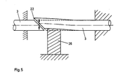
- each of the N modulators 20 is configured as a total-reflection optomechanical modulator (FIG. 5).
- Each modulator consists of an optical fiber or of the integrated optical waveguide 3, in which a wrong to Arranged beam direction separating gap 22 is located, the gap width can be modulated by a piezoelectric actuator 26 between zero and a maximum distance in the order of one or a few wavelengths of light. If the gap width is reduced to zero, then the light fed into the waveguide will propagate practically free of reflection via the cleavage site and reach the corresponding optical waveguide 3 of the assembly 13. When the gap 22 is opened, a light fraction which is initially proportional to the gap width is reflected away from the gap in such a way that correspondingly less light is incident on the optical waveguide of the assembly 13.
- each of the optical modulators 20 is designed as an electro-optical modulator (FIG. 6).
- the waveguide 3 itself is made of an electro-optically active material or covered as a cladding layer 27. By applying an electric field, the refractive index of this material can be changed so that the optical conditions for the guidance of the light in the waveguide are changed and thereby the transmitted luminous flux is modulated accordingly.
- the integrated optical structure 13 serves to distribute the image information: Due to the low scattering and absorption, the coupled into the optical waveguide 3 light in the normal state undisturbed transmitted through the waveguide and leaves it at the other end. A scattering in the space perpendicular to the direction of the waveguide does not take place practically. Any attenuation losses in each line can be compensated to achieve a uniform brightness in the decoupling described later on the time course of the intensity of the respective light source.
- the integrated optical structure for spatial distribution of the image information represented by the N parallel waveguides 3 can be produced in various embodiments (FIG. 7).
- N are integrated with parallel optical waveguides 3 on a transparent substrate 28 (see Fig. 7b).
- the substrate may, for example, consist of a polished glass plate on which silver ions in the desired waveguide geometry are diffused into the glass surface by means of a known photolithographic technique.
- the diffusion mask is removed. Obtained in this way N embedded parallel mono- or multi-mode waveguide 3 of approximately half-moon-shaped cross-section.
- the light fed into such a waveguide undergoes total reflection at both the waveguide / glass substrate interface and at the waveguide / air interface such that it can propagate along the waveguide with little loss.
- Integrated optical strip conductors of the described form can be produced not only by means of the sketched in-diffusion method.
- Other implementation options are z. B .: - Pressing and filling of polymer or mixed oxide matrix selective etching and oxidation of silicon, - photo-induced self-condensation etc.
- N are mounted on the surface of a plane polished glass plate 29 by means of a transparent polymer adhesive under parallel optical fibers 3.
- the glass plate prepared in this way is then abraded down and plan polished auricularly exactly half the glass fiber thickness. Again, within the core of each fiberglass, there is an optical fiber 3 with an approximate crescent-shaped cross-section.
- the integrated optical light distribution structure 13 is superimposed on the pixel coupling-out structure 14.
- This typically consists of a number of M strip-shaped, perpendicular to the waveguides 3 mounted and possibly further structured electrodes 1. These form with the optical waveguides a kind of grid with M ⁇ N crossing points 5, which represent the pixels of the display substantially.
- a column is then serially activated in each case and at the same time the light diodes corresponding to a more or less bright pixel in this column are excited in pulsed fashion in parallel operation in accordance with the desired brightness. Then the process is repeated for the next column.
- a corresponding result can be achieved in another embodiment of the electro-optical assembly by means of light transmission modulation.
- the pixel extraction structure 14 driven via the strip electrodes can be realized in various embodiments. To distinguish between two main embodiments: a piezoelectrically driven micromechanical variant and - An electro-optical or thermo-optical variant.
- the decoupling structure is achieved by means of a modulation of the total reflection at the surface of the optical waveguides 3 which is dependent on the activation of the strip electrodes 1.
- this interface for each light guide is brought into optical contact simultaneously with a column stick.
- This optical contact causes each light guide at a certain time on the same image column radiates out to this place outgoing light to the outside.
- a special scan of the image columns from the first to the second The latter allows the entire length of the optical fibers and thus the entire surface of the screen to be scanned sequentially.
- the light guided in the waveguide leaves this waveguide through the contact surface at a shallow angle. It is therefore necessary to divide this exit angle by means of an additional optical component such that the light led out thereafter is emitted approximately perpendicular to the plane formed by the optical fibers.
- the strip electrodes are designed in two parts for this purpose (FIG. 8) and thus consist of two superimposed transparent electrodes 30 and 31 for each column. A piezoelectric, transparent layer is formed between these electrodes for each column 32 arranged. In addition, a transparent contact layer 33 may be provided as an insulator layer. The thus modified strip electrodes are fixed on a transparent cover layer 34.
- the thickness of the piezoelectric intermediate layers 32 is reduced by an applied voltage, there is always a gap between the driven optical waveguides 3 and the insulator layer in the live state 33 available.
- the air gap between the waveguides and the column rod is reduced to zero, so that now no longer the air but the electrode material or a special insulation layer form the adjacent phase to the waveguide.
- the change in refractive index of the adjacent medium caused by the change of the neighboring phase leads to a local light extraction.
- each of the stripe-shaped piezoelectric intermediate layers 32 has a greater refractive index than its surroundings, lateral scattering of the light is practically excluded within these intermediate layers.
- the observer therefore recognizes each intersection and point of contact between an optical waveguide and an insulator layer as a luminous pixel, the brightness of which is proportional to the light intensity which is input to the corresponding waveguide.
- the light in the same half-plane in which it emerges from the light guides, is supplied to the observer. This means that the light must pass through the piezoelectric column structure (column bar), which causes the optical contact on and off vertically.
- the light guided out of the light guides is reflected by means of special mirror strips 39 arranged in the direction of the column in such a way that it illuminates Passing optical fiber approximately perpendicular to their optical axes and the transparent substrate plate traversed to then reach the observer.
- the light exits the entire active screen in the half-plane, which is opposite to that in which it first left the optical fibers.
- the mirror strips 35 in this case consist of a first and second prismatic element 39a and 39c, with mirror layer 39b therebetween.
- the decoupling of the light from the respective optical waveguide induced by a voltage signal at the column electrodes is achieved by means of electro-optical or thermo-optical methods, which are described in more detail below and are schematically sketched in FIG.
- electro-optical or thermo-optical methods which are described in more detail below and are schematically sketched in FIG.
- the refractive index of a material component is changed either directly electro-optically by the applied electric field or indirectly by the locally generated Joule heat caused by temperature increase.
- Direct electro-optical decoupling is described schematically in FIG. 10a.
- the refractive index of the insulator layer 2 of the embodiment of the display shown in FIG. 1 is changed so that a low-loss guidance of the light in the waveguide 3 is no longer possible.
- the change is achieved by the electric field, which when applying a voltage to two adjacent or above and below the waveguide arranged strip electrodes 1 and 1 and 36 is formed.
- the refractive index change At the location locally and temporarily modified by the refractive index change, coupling of the waveguide modes conducted up to this point to the continuum of the radiating modes in the outer space therefore takes place. This means that locally the condition for the total internal reflection is undershot (see right part of Fig. 10a).
- the preferred direction of the light emission is determined by the type of modes and the achievable refractive index difference. This will be relatively small, determined by the materials used. Typical values for the difference between the refractive index n a of the insulator material and n f of the waveguide material are between a few 10 ⁇ 2 and 10 ⁇ 3. The main radiation thus takes place at a very shallow angle relative to the surface.
- An improvement in the Abstrahl characterizing can be achieved either by a strong scattering layer or by an optimized diffraction grating on the insulator material or by an insulator material with a suitable refractive index gradient for deflecting the light.
- Suitable materials for the realization of the electro-optical isolator layer include the following substances: Potassium niobate, lithium niobate, Lead oxide, lead zirconate titanate (PZT), lead anthracene zirconate titanate (PLZT), - polydiacethylenes, - paranitroanilines, electro-optical dyes in polymer matrices, - Stilbene in Langmuir-Blodgett films, etc.
- thermo-optical change of the refractive index of the insulator layer can this also by a local Temperature increase, caused by the Joule heat generated by an electric current influence (Fig. 10b). Otherwise, this method of direct thermo-optically induced decoupling corresponds to the method discussed above.
- the ablation angle is essentially determined by the locally electro-optically achievable refractive index difference in the insulator material.
- suitable shaping of the cover electrode 3 it is possible to achieve a periodic modulation of the refractive index and thereby produce a temporally variable phase grating. On the one hand, this results in a more efficient coupling between the waveguide methods and a broken wave, ie emerging from the display plane to the front.
- suitable choice of the lattice parameters it is also possible to influence the emission angle, ie in particular to achieve larger emission angles (FIG. 10c) ).
- each column electrode 1 is formed into a comb 37 of limited width each.
- each of the columns could be about 100 ⁇ m wide and thus comprise a number of periods.
- the counter-electrode 36 is to be applied between the substrate 4 and the waveguide layer 3.
- the waveguide 3 contains trapped microdroplets 38 of a nematic-liquid crystalline material.
- An applied electric field causes turbulence in the liquid-crystalline phase 38 and thereby induces scattering of the light guided in the waveguide 3. This scattering is based on the fact that the optical properties of the liquid-crystalline microdroplets are anisotropic, ie they have a different refractive index in different directions.
- the material appears homogeneous and scattering does not occur.
- the preferential orientation is lost or the orientation is reoriented, the waveguide material becomes inhomogeneous and consequently scatters the light previously guided in the waveguide.
- the electrically induced local change of the orientation in the microdroplets thus leads to a radiation to the outside and thus to a bright spot on the display.
- Such a scattering can also be achieved by the method shown schematically in FIG. 10 e, in which the waveguide is constructed according to the principle of the Christiansen filter.
- the waveguide here also consists of two phases whose refractive index n1 and n f in the normal state, ie at a temperature T1 match, but have a different temperature coefficient of the refractive index. By locally increasing the temperature, different results occur for both phases Refractive indices and thus a scattering of the guided in the waveguide until then light.
- the integrated optical structure for the distribution of the image information contains for each color separate waveguides or -
- the color control is done in time division by sequential coupling of different colors in the same distribution structure.
- FIG. 11 shows a light source 40 whose light is transmitted through a condenser 41. From there, the collimated light reaches a filter wheel 42, which can be rotated by a motor 43 in rotation. At the periphery of the filter wheel color filters are provided, preferably in the colors cyan, yellow and magenta.
- a light guide 44 is arranged, which passes the filtered light to a light distributor optics 45.
- the color control takes place in time-division multiplexing.
- a first light-emitting diode 46 is provided, which shines for example in the color magenta.
- a second LED 47 lights up For example, in the color yellow.
- the light of both light-emitting diodes is aligned in parallel by lenses 48 and impinges on a dichroic mirror 49.
- the light passing through this semi-transparent mirror is reflected by a collimator 50 onto the input 5 of a light guide 52 and leaves the light guide and then exits in a light distribution optics 53.
- Pos. 54 indicates a control for the two light emitting diodes 46, 47.
- the screen according to the invention is thus an active screen in which the following essential functional elements can be distinguished: - light generation and image content modulation, - two-dimensional spatial light distribution and - Light extraction.
- the light generation is done by means of known light sources, which in some embodiments also allow direct image content (light / dark) modulation. Other embodiments use special modulators.
- the spatial light distribution occurs via an integrated optical waveguide array or an array of glass fibers.
- the spatially distributed light extraction takes place via electro-optical, thermo-optical or optomechanical methods.
- the integrated-optical light distribution structure is linked to a structure of parallel electric stripe electrodes running perpendicular thereto. The intersections of these strip electrodes with the optical waveguides define the Pixels.
- the activation of the strip electrodes (decoupling) is synchronized with the picture content modulation.
Abstract
Description
Die Erfindung betrifft einen aktiven Bildschirm in Flachbauweise mit in zwei Gruppen, nämlich in Zeilen und in Spalten angeordneten Signalleitungen, die an ihren Kreuzungspunkten Bildpunkte des Bildschirms definieren, mit einer Steuerung und Signalaufbereitung für die den Signalleitungen zugeleiteten Bildinformationen und mit wenigstens einem Lichtelement, das an jedem Kreuzungspunkt entspechend moduliertes Licht aussendet.The invention relates to an active screen in flat construction with arranged in two groups, namely in rows and in columns signal lines that define at their crossing points pixels of the screen, with a control and signal conditioning for the signal lines fed image information and at least one light element that on emits modulated light according to each crossing point.
Derartige aktive Bildschirme sind bekannt, bei denen die Bildpunkte durch Flüssigkristalle erzeugt werden. Beide Gruppen der Signalleitungen sind hierbei durch elektrische Leitungen ausgebildet, wobei sich an deren Kreuzungspunkten jeweils der Flüssigkristall befindet. Die bekannten Bildschirme benötigen zu ihrer Funktion an jedem Kreuzungspunkt ein aktives elektronisches Schaltelement (eine Diode oder einen Transistor). Sie sind deshalb relativ schwierig herzustellen. Diese bekannten Bildschirme weisen überdies eine beschränkte Bildwechselfrequenz, Bildauflösung und einen sehr beschränkten Kontrastumfang auf, der sich für eine wirklichkeitsnahe Darstellung von Fernsehbildern oder auch für eine ermüdungsfreie Darstellung von Informationen auf Monitoren nur schlecht eignet.Such active screens are known in which the pixels are generated by liquid crystals. Both groups of the signal lines are in this case formed by electrical lines, wherein at their crossing points in each case the liquid crystal is located. The known screens require an active electronic switching element (a diode or a transistor) for their function at each crossing point. They are therefore relatively difficult to produce. These known screens also have a limited frame rate, image resolution and a very limited range of contrast, which is poorly suited for a realistic representation of television images or for a fatigue-free display of information on monitors.
Ein anderer bekannter Typ derartiger aktiver Bildschirme verwendet miniaturisierte Elektronenstrahlröhren, wobei der Elektronenstrahl um etwa 90 abgelenkt wird und auf eine neben der Elektronenkanone angeordnete Fluoreszenzschicht auftrifft. Diese aktiven Bildschirme sind jedoch für viele Anwendungszwecke ungeeignet, da sie eine verhältnismäßig große Bautiefe aufweisen.Another known type of such active screens employs miniaturized electron guns wherein the electron beam is deflected by about 90 and impinges on a fluorescent layer adjacent to the electron gun. However, these active screens are unsuitable for many applications because they have a relatively large overall depth.
Die Erfindung vermeidet diese Nachteile. Ihr liegt die Aufgabe zugrunde, einen aktiven Bildschirm vorzuschlagen, der in Flachbauweise hergestellt werden kann und sich insbesondere durch eine gute Bildwechselfrequenz, Bildauflösung und einen guten Kontrastumfang auszeichnet, so daß der erfindungsgemäße Bildschirm insgesamt für eine wirklichkeitsnahe Darstellung von Fernsehbildern und anderen Informationen geeignet ist. Der erfindungsgemäße Bildschirm soll vorzugsweise in kleinem Format ausgeführt werden können, so daß er auf kurze Distanz mit dem bloßen Auge, mit einer Lupe oder auch mit einem Okular betrachtet werden kann.The invention avoids these disadvantages. It is the object of the invention to propose an active screen that can be manufactured in a flat design and is characterized in particular by a good frame rate, image resolution and a good contrast, so that the screen of the invention is generally suitable for a realistic representation of television images and other information. The screen according to the invention should preferably be able to be made in a small format, so that it can be viewed at a short distance with the naked eye, with a magnifying glass or with an eyepiece.
Zur Lösung dieser Aufgabe ist die Erfindung dadurch gekennzeichnet, daß eine der beiden Gruppen der Signalleitungen durch Lichtwellenleiter gebildet wird, in die eingangsseitig das modulierte Lichtsignal eingekoppelt wird und die an jedem der Kreuzungspunkte eine von der Steuerung beaufschlagbare Einrichtung zum Auskoppel des in diesem Lichtwellenleiter vorhandenen optischen Signals in einer im wesentlichen senkrecht zur Ebene des Bildschirms verlaufenden Richtung aufweisen.To achieve this object, the invention is characterized in that one of the two groups of signal lines is formed by optical fibers, in the input side, the modulated light signal is coupled and at each of the crossing points acted upon by the controller means for decoupling present in this optical waveguide optical Have signal in a direction substantially perpendicular to the plane of the screen direction.
Über die erfindungsgemäß verwendeten Lichtwellenleiter erhält man somit eine gute optische Qualität des vom Bildschirm abgestrahlten Bildes. In die Lichtwellenleiter wird eingangsseitig das entsprechend modulierte optische Signal eingekoppelt und an den Kreuzungspunkten wird das Signal ausgekoppelt und ergibt somit den betreffenden Bildpunkt bzw. in der Gesamtheit der Bildpunkte das Bild. Über die zweite Gruppe der Signalleitungen, im allgemeinen elektrische Signalleitungen (Streifenelektroden) und die zugeordnete Steuerung wird das Bild des Bildschirms sequentiell aufgebaut, d. h. die Bildpunkte des Bildschirmes werden parallel zueinander oder nacheinander in jeder Zeile und nacheinander Zeile für Zeile in so kurzer Folge erregt, daß sich das Bild für den Betrachter ergibt.By means of the optical waveguides used according to the invention, a good optical quality of the image radiated from the screen is thus obtained. In the optical fibers On the input side, the correspondingly modulated optical signal is coupled in and the signal is coupled out at the crossing points and thus results in the relevant pixel or in the entirety of the pixels the image. Via the second group of signal lines, generally electrical signal lines (strip electrodes) and the associated control, the image of the screen is constructed sequentially, ie the pixels of the screen are excited parallel to each other or successively in each line and successively line by line in such a short sequence, that the picture results for the viewer.
Bevorzugte Ausführungsformen der Erfindung sind in den Unteransprüchen angegeben.Preferred embodiments of the invention are specified in the subclaims.
Die Erfindung wird im folgenden anhand von Ausführungsbeispielen näher erläutert, aus denen sich weitere wichtige Merkmale ergeben. Es zeigt:
- Fig. 1 schematisch und perspektivisch eine Darstellung zur Erläuterung des Grundprinzips der Erfindung;
- Fig. 2 ebenfalls schematisch und perspektivisch die einzelnen Baugruppen, die den erfindungsgemäßen Bildschirm aufbauen;
- Fig. 3 schematisch und perspektivisch eine Ausführungsform der Einrichtung zur Lichterzeugung und Lichtmodulation in den Wellenleitern;
- Fig. 4a
bis 4c einen hierbei verwendeten optischen Lamellenmodulator; - Fig. 5 das Prinzip eines optomechanischen Totalreflexions-modulators;
- Fig. 6a perspektivisch ein elektrooptisches Modulatorarray;
- Fig. 6b eine Stirnansicht von Fig. 6 a;
- Fig. 7a eine erste Ausführungsform des Aufbaus einer integriert-optischen Struktur zur Verteilung der Bildinformation;
- Fig. 7b eine zweite Ausführungsform dieses Aufbaus;
- Fig. 8 schematisch eine Anordnung mit einem piezoelektrisch getreibenen, mikromechanischen Schalter mit Abstrahlung durch Spaltenstäbchen;
- Fig. 9 eine Anordnung ähnlich Fig. 8 mit Abstrahlung durch ein Substrat;
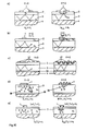
- Fig. 10a
bis 10e eine schematische Darstellung verschiedener Auskopplungsmethoden, und zwar jeweils links in diesen Figuren in nicht ausgekoppeltem Zustand und rechts in ausgekoppeltem Zustand; - Fig. 11 eine Darstellung zur Eläuterung der Farbansteuerung mit Zeitmultiplexverfahren über Filter;
- Fig. 12 eine Ausführungsform der Farbansteuerung im Zeitmultiplexverfahren.
- Fig. 1 shows schematically and in perspective a representation for explaining the basic principle of the invention;
- Fig. 2 also schematically and in perspective, the individual modules that build the screen according to the invention;
- Fig. 3 schematically and in perspective an embodiment of the means for light generation and light modulation in the waveguides;
- Fig. 4a
to 4c a here used optical slat modulator; - 5 shows the principle of an optomechanical total reflection modulator;
- 6a shows in perspective an electro-optical modulator array;
- Fig. 6b is an end view of Fig. 6 a;
- 7a shows a first embodiment of the structure of an integrated-optical structure for distributing the image information;
- Fig. 7b shows a second embodiment of this construction;
- 8 schematically shows an arrangement with a piezoelectrically driven micromechanical switch with radiation through column rods;
- FIG. 9 shows an arrangement similar to FIG. 8 with radiation through a substrate; FIG.
- Fig. 10a
to 10e is a schematic representation of different extraction methods, in each case on the left in these figures in the uncoupled state and on the right in the uncoupled state; - FIG. 11 shows a representation for the purpose of outlining the color activation with time-division multiplexing via filters; FIG.
- 12 shows an embodiment of the color control in the time-division multiplex method.
Mit der vorliegenden Erfindung soll ein vorzugsweise kleinformatiger, aktiver Bildschirm in Flachbauweise geschaffen werden, dessen Betrieb ohne nachteilige Beeinflussung der Lichtausbeute und des Kontrastes mit geringer elektrischer Leistung möglich ist und mit dem sich tragbare, miniaturartige Video-Displays realisieren lassen.With the present invention is a preferably small-sized, active screen in flat design be created whose operation is possible without adversely affecting the light output and the contrast with low electrical power and can be realized with the portable, miniature video displays.
Hierzu zeigt Fig. 1 als Prinzipdarstellung eine erste Gruppe von in Spalten angeordneten Streifenelektroden 1. An der Unterseite der Streifenelektroden befindet sich eine Schicht, die als Einrichtung 2 zur Lichtauskopplung dient. Darunter wiederum befindet sich eine zweite Gruppe von in Zeilen angeordneten Lichtwellenleitern 3. Die Anordnung ist auf einen Träger 4 aufgebracht.1 shows a schematic representation of a first group of
Die Kreuzungspunkte 5 zwischen den Streifenelektroden 1 und den Lichtwellenleitern 3 stellen die Bildpunkte des aktiven Bildschirms dar. Hierzu ist in Fig. 1 bei Pos. 5 angedeutet, wie dort das Licht in den oberen Halbraum abgestrahlt wird. Die Pfeile links in Fig. 1 symbolisieren die bereits entsprechend der Bildinformation hell/dunkel modulierten Lichtsignale. Die integriert-optische Wellenleiterstruktur mit den Lichtwellenleitern 3 bewirkt die zweidimensionale, räumliche Verteilung der Lichtsignale. Eine Ansteuerung der kreuzenden Elektroden 1 erlaubt die Auskopplung der Lichtsignale an den bestimmten Bildpunkten oder Kreuzungspunkten 5.The crossing points 5 between the
Fig. 2 zeigt die wesentlichen Baugruppen eines aktiven Bildschirms unter grundsätzlicher Verwendung der in Fig. 1 skizzierten Anordnung. Daraus ergibt sich, daß ein Video-Eingangssignal über eine Leitung 7 in eine Bildsignalaufbereitungs-Elektronik 8 eingegeben wird. Das Video-Eingangssignal gelangt außerdem gleichzeitig zu einer Zeitsynchronisations- und Steuerelektronik 9, die über eine weitere Leitung 10 auch an die Elektronik 8 angeschlossen ist. Die Ausgangssignale der Elektronik 9 gelangen außerdem zu einer Ansteuerungselektronik 11 für die Streifenelektroden.Fig. 2 shows the main components of an active screen with the basic use of the sketched in Fig. 1 arrangement. As a result, a video input signal is input via a
An die Ausgänge der Elektronik 8 ist eine Bildsignalerzeugungs-Elektrooptik 12 angeschlossen und an deren Ausgänge wiederum eine integriert-optische Struktur 13 zur Verteilung der Bildinformation. Diese widerum ist verbunden mit einer Bildpunkt-Auskoppelstruktur 14, die von den Ausgängen der Elektronik 11 angesteuert wird.To the outputs of the electronics 8, an image signal generating electro-
Über die Leitung 10 werden Synchronissationssignale in die Elektronik 8 abgegeben und über Leitungen 15 werden am Ausgang der Eletronik 8 anstehende, parallele elektrische Bildsignale in den Eingang der Elektrooptik 12 eingegeben. Am Ausgang dieser Elektrooptik 12 werden wiederum über Leitung 16 parallele, optische Bildsignale in die Struktur 13 eingegeben. Die Leitungen 17 schließlich deuten die sequentiell-elektrische Ansteuerung der Struktur 14 an.About the
Die schraffierten Baugruppen 12, 13, 14 bilden den eigentlichen Kern des erfindungsgemäßen Bildschirms, während die weiteren Baugruppen 8, 9 11 and sich bekannt sind. Die Strukturen 13, 14 entsprechen im wesentlichen der anhand von Fig. 1 erläuterten Anordnung.The hatched
Die Anordnung nach Fig. 2 arbeitet grundsätzlich wie folgt.The arrangement of FIG. 2 basically works as follows.
Die Bildsignalaufbereitungs-Elektronik 8 erhält beispielsweise ein normiertes Televisions-Videosignal, welches Zelie für Zeile seriell übermittelt wird. Ein derartiges Signal enthält 2×25-mal pro Sekunde ein im Zeilensprungverfahren kodiertes Fernsehbild. Die Elektronik 8 speichert ein erstes serielles vollständiges Bild und übermittelt dieses Bild nach Seriell-Parallel-Konversion in derjenigen Zeitspanne an die elektrooptische Baugruppe 12, während welcher das zweite Bild in den Speicher eingelesen wird.The image signal processing electronics 8 receives, for example, a normalized television video signal, which Zelie serially transmitted by line. Such a signal contains 2 × 25 times per second an interlaced coded television picture. The electronics 8 stores a first serial full picture and transmits this image to the electro-
Wenn man von einem Bild mit N Zeilen ausgeht, dann wird in der Elektronik-Baugruppe 8 die analog-elektrisch kodierte Videoinformation jeder Zeile gespeichert und, um den Faktor N zeitlich gedehnt, auf jeder der N Bildsignallinien gleichzeitig, d. h. parallel, in die eltrooptische Baugruppe 12 eingespeist. Je nach Ausführungsform der erfindungsgemäßen Baugruppe 12 müssen hierbei die eingespeisten parallelen und zeitlich gedehnten Zeilen-Videosignale spannungs- und impedanzmäßig an die entsprechenden elektrooptischen Signalwandler angepaßt werden.Assuming a picture with N lines, then in the electronics package 8, the analog-electrically coded video information of each line is stored and, time-stretched by the factor N, on each of the N picture signal lines at the same time, d. H. parallel, fed into the electro-
Die bildsignalerzeugende Elektrooptik-Baugruppe 12 kann in verschiedenen Ausführungsformen realisiert werden.The image signal generating electro-
In einer ersten Ausführungsform treiben die N Bildsignallinien eine Linearanordnung von N elektrolumineszenten Halbleiterdioden, welche ihre Zeilenbildsignale ihrerseits in die N optischen Glasfasern oder integriert optischen Wellenleiter einspeisen. In Fig. 2 sind diese N Lichtleiter symbolisch als Verbindungen zwischen den Baugruppen 12 und 13 dargestellt. In dieser ersten Ausführungsgorm werden die N Leuchtdioden oder Halbleiter-Laser vorzugsweise zusammen auf einem Substrat in integrierter oder in Hybrid-Technik aufgebaut. Diese Bauweise erlaubt es, die zur Einkopplung in die N Lichtleiter notwendige hohe Justiergenauigkeit zu erreichen.In a first embodiment, the N picture signal lines drive a linear array of N electroluminescent semiconductor diodes which in turn feed their line picture signals into the N optical fibers or integrated optical waveguides. In Fig. 2, these N optical fibers are shown symbolically as connections between the
Mit heute üblichen Leuchtdioden hoher Effizienz lassen sich bei einem Strom von ca. 20mA Ausgangssignale von etwa 120mCd erreichen. Nimmt man an, daß im Mittel jeweils die Hälfte der Bildpunkte einer Spalte, also die Hälfte aller jeweils einer Zeile entsprechenden Dioden, hell sind, und berücksichtigt alle nachfolgenden Verluste durch einen Faktor 100, so ergibt sich als Beispiel für einen 5×5 cm² großen Display mit 600 Zeilen ein Wert von 144 Cd/m². Dieser Wert ist als mittlere Helligkeit für einen Display ausreichend.With today's usual high efficiency LEDs can be at a current of about 20mA output signals of about 120mCd to reach. If one assumes that on average half of the pixels of a column, ie half of all diodes corresponding to one row, are bright, and takes into account all subsequent losses by a factor of 100, the result is an example of a 5 × 5 cm² large one Display with 600 lines a value of 144 cd / m². This value is sufficient as average brightness for a display.
Die Anzahl der benötigten Leuchtdioden läßt sich durch Verwendung von integriert optischen Richtungskopplern zur sequentiellen Ansteuerung mehrere Zeilen mit einer Leuchtdiode evtl. verringern.The number of light-emitting diodes required can possibly be reduced by using integrated optical directional couplers for the sequential control of several lines with one light-emitting diode.
In einer zweiten Ausführungsform der elektrooptischen Baugruppe 12 werden die Lichterzeugungs- und die Lichtmodulations-Funktionen getrennt.In a second embodiment of the electro-
Die Lichterzeugung wird hierbei vorzugsweise durch eine spezielle (Niedervolt-) Glühlampe 18 realisiert, welche eine gerade gestreckte Glühwendel enthält. (vgl. Fig. 3) Das von der Wendel ausgehende Lichtbündel wird über einen optischen Kondensor oder über einen Lichtleiter 21 mit großem Kerndurchmesser sowie über ein optisches Faserbündel 19 auf die in einer geraden Linie angeordneten N Eingangspupillen einer Reihe von N elektrooptischen Modulatoren 20 abgebildet.The light generation is in this case preferably realized by a special (low-voltage)
Die N Modulatoren 20 werden hierbei von den N elektrischen Bildsignallinien parallel angesteuert. Die von den N Modulatoren zeitlich gesteuerten optischen Bildsignale werden entweder mittels eines Objektivs oder vorzugsweise über Lichtleiter in die N Eingänge der Baugruppe 13 eingespeist.The N modulators 20 are in this case driven in parallel by the N electrical image signal lines. The temporally controlled by the N modulators optical image signals are fed either by means of an objective or preferably via optical fibers in the N inputs of the
Die in Reihe angeordneten N elektrooptischen Modulatoren können hierbei wiederum in verschiedenen Ausführungsformen realisiert werden.The series-arranged N electro-optical modulators can in this case in turn be realized in various embodiments.
In einer ersten Ausführungsform besteht jeder Modulator 20 aus einem Eingangspolarisator, einer elektrooptischen Kerr-Zelle und aus einem Ausgangspolarisator. Die Polarisatoren sind hierbei derart angeordnet, daß die Modulatorzelle im spannungslosen Zustand das einfallende Licht blockiert und bei Anlegen eines Video-Zeilensignals eine entsprechend zeitlich modulierte Lichtintensität durchläßt. Die N Kerr-Zellen können hierbei vorzugsweise als hybrid-integrierte elektrooptische Keramik vom PLZT-Typ oder als elektrooptisch aktive Polymerplättchen ausgebildet werden, welche auf einer Substratplatte montiert sind.In a first embodiment, each modulator 20 consists of an input polariser, an electro-optic Kerr cell, and an output polariser. The polarizers are in this case arranged such that the modulator cell blocks the incident light in the de-energized state and transmits a correspondingly time-modulated light intensity upon application of a video line signal. The N Kerr cells may preferably be formed as a hybrid integrated PLZT-type electro-optic ceramic or as electro-optically active polymer platelets mounted on a substrate plate.
In einer zweiten Ausführungsform (Fig. 4) ist jeder der N Modulatoren 20 als piezoelektrisch, elektrodynamisch, elektromagnetisch oder elektrostatisch stellbare Blendenlamelle 25 ausgeführt. Diese taucht mehr oder weniger tief in einen Trennspalt 22 jeweils eines Wellenleiters 3 oder einer optischen Faser ein und schwächt so den Lichtstrom proportional zu ihrer Stellung. (S. Pfeile 24 in Fig. 4b)
Fig. 4a zeigt auch einen Lamellenhalter 23 und Fig. 4c erläutert die hierbei vorgesehene Polanordnung (N = Nordpol; S = Südpol).In a second embodiment (FIG. 4), each of the
FIG. 4 a also shows a
In einer dritten Ausführungsform ist jeder der N Modulatoren 20 als optomechanischer Totalreflexions-Modulator ausgebildet (Fig. 5). Jeder Modulator besteht hierbei aus einer Lichtleiterfaser oder aus dem integriert optischen Wellenleiter 3, in welchem sich ein schief zur Strahlrichtung angeordneter Trennspalt 22 befindet, dessen Spaltbreite durch ein piezoelektrisches Stellelement 26 zwischen Null und einem maximalen Abstand in der Größenordnung von einer oder einigen Lichtwellenlängen moduliert werden kann. Wenn die Spaltbreite auf Null reduziert wird, dann wird das in den Wellenleiter eingespeiste Licht sich praktisch reflexionsfrei über die Spaltstelle fortpflanzen und den entsprechenden Lichtwellenleiter 3 der Baugruppe 13 erreichen. Bei Öffnung des Spalts 22 wird ein anfangs zur Spaltbreite proportionaler Lichtbruchteil aus dem Spalt wegreflektiert derart, daß entsprechend weniger Licht in den Lichtwellenleiter der Baugruppe 13 einfällt.In a third embodiment, each of the
In einer weiteren Ausführungsform ist jeder der optischen Modulatoren 20 als elektrooptischer Modulator ausgebildet (Fig. 6). Hierbei wird der Wellenleiter 3 selbst aus einem elektrooptisch aktiven Material hergestellt oder damit als Claddingschicht 27 überdeckt. Durch Anlegen eines elektrischen Feldes läßt sich der Brechungsindex dieses Materials derart verändern, daß die optischen Bedingungen für die Führung des Lichtes in dem Wellenleiter verändert werden und dadurch der transmittierte Lichtstrom entsprechend moduliert wird.In a further embodiment, each of the
Weitere Ausführungsformen können auf der Basis von anderen, an sich bekannten fiberoptischen Lichtmodulatoren realisiert werden; z. B. Mikrokrümmungsmodulatoren, Polarisationszustands-Modulatoren etc.Other embodiments may be realized on the basis of other fiber optic light modulators known per se; z. Microbend modulators, polarization state modulators etc.
Die integreiert-optische Struktur 13 dient zur Verteilung der Bildinformation:
Aufgrund der geringen Streuung und Absorption wird das in die Lichtwellenleiter 3 eingekoppelte Licht im Normalzustand ungestört durch die Wellenleiter transmittiert und verläßt diese am anderen Ende. Eine Streuung in den Raum senkrecht zur Richtung der Wellenleiter findet praktisch nicht statt. Eventuelle Dämpfungsverluste in jeder Zeile lassen sich zur Erzielung einer gleichmäßigen Helligkeit bei der später beschriebenen Auskopplung über den zeitlichen Verlauf der Intensität der jeweiligen Lichtquelle kompensieren.The integrated
Due to the low scattering and absorption, the coupled into the
Die durch die N parallelen Wellenleiter 3 repräsentierte integriert optische Struktur zur räumlichen Verteilung der Bildinformation kann in verschiedenen Ausführungsformen hergestellt werden (Fig. 7).The integrated optical structure for spatial distribution of the image information represented by the N
In einer ersten Ausführungsform werden N unter sich parallele Lichtwellenleiter 3 auf ein transparentes Substrat 28 integriert (s. Fig. 7b). Das Substrat kann hierbei beispielsweise aus einer polierten Glasplatte bestehen, auf welcher vermittels einer bekannten photolithographischen Technik Silberionen in der gewünschten Wellenleitergeometrie in die Glasoberfläche eindiffundiert werden. Nach Abschluß dieses Diffusionsprozesses wird die Diffusionsmaske entfernt. Man erhält auf diese Weise N eingebettete parallele Mono- oder Multimode-Wellenleiter 3 von etwa halbmondförmigem Querschnitt. Das in einen derartigen Wellenleiter eingespeiste Licht erfährt hierbei sowohl an der Wellenleiter-Glassubstrat-Grenzschicht wie auch an der Wellenleiter-Luft-Grenzfläche eine Totalreflexion derart, daß es sich verlustarm entlang dem Wellenleiter fortpflanzen kann. Integriert optische Streifenleiter der beschriebenen Form können nicht nur mittels der skizzierten Eindiffusions-Methode hergestellt werden. Andere Realisierungsmöglichkeiten sind z. B.:
- Eindrücken und Verfüllen von Polymer- oder Mischoxidmatrix
- selektives Ätzen und Oxidieren von Silizium,
- photoinduzierte Selbstkondensation etc.In a first embodiment, N are integrated with parallel
- Pressing and filling of polymer or mixed oxide matrix
selective etching and oxidation of silicon,
- photo-induced self-condensation etc.
In einer zweiten, optischen nahezu gleichwertigen Ausführungsform werden N unter sich parallele optische Glasfasern 3 vermittels eines durchsichtigen Polymer-Klebstoffes auf die Oberfläche einer planpolierten Glasplatte 29 montiert. In einem nächsten Arbeitsgang wird hierauf die derartig vorbereitete Glasplatte aur ziemlich genau die halbe Glasfaserdicke heruntergeschliffen und planpoliert. Es ergibt sich wiederum innerhalb des Kerns jeder Glasfiber ein Lichtleiter 3 mit approximativ halbmondförmigem Querschnitt.In a second, almost equivalent, optical embodiment, N are mounted on the surface of a plane polished
Der integriert optischen Lichtverteilungsstruktur 13 wird die Bildpunkt-Auskoppelstruktur 14 überlagert. Diese besteht typischerweise aus einer Anzahl von M streifenförmigen, senkrecht zu den Wellenleitern 3 angebrachten und evtl. noch weiter strukturierten Elektroden 1. Diese bilden mit den Lichtwellenleitern eine Art Gitter mit M×N Kreuzungspunkten 5, die im wesentlichen die Bildpunkte des Displays repräsentieren. Durch eine geeignete Ansteuerung der Spaltenelektroden 1 wird erreicht, daß die Bedingung für die fast verlustlose Führung des Lichts im jeweiligen Wellenleiter nicht mehr erfüllt ist. Entsprechend wird die Lichtquelle nun nach außen abgestrahlt und in den Halbraum vor dem Display zum Betrachten freigegeben.The integrated optical
Um eine Lichtemission bzw. Lichtauskopplung zu erhalten, muß Licht in die entsprechende Zeile eingekoppelt werden und die entsprechende Spalte muß gleichzeitig aktiviert sein. In der einfachsten Realisierung genügt es, die im Normalzustand deaktivierten Spalten seriell über eine binäre Information zu aktivieren. Die eigentlichen Bildinformationen, d. h. Helligkeit und Graustufen, werden durch die Intensität des modulierten eingekoppelten Lichts vermittelt.In order to obtain a light emission or light outcoupling, light must be coupled into the corresponding line and the corresponding column must be activated at the same time. In the simplest realization, it is sufficient to serially disable the normally-disabled columns via binary information to activate. The actual image information, ie brightness and gray levels, are mediated by the intensity of the modulated injected light.
Zum Scannen des Displays wird dann seriell jeweils eine Spalte aktiviert und gleichzeitig werden die einem mehr oder weniger hellen Bildpunkt in dieser Spalte entsprechenden Leuchtdioden im Parallelbetrieb pulsförmig entsprechend der gewünschten Helligkeit erregt. Anschließend wird der Vorgang für die jeweils nächste Spalte wiederholt.For scanning the display, a column is then serially activated in each case and at the same time the light diodes corresponding to a more or less bright pixel in this column are excited in pulsed fashion in parallel operation in accordance with the desired brightness. Then the process is repeated for the next column.
Ein entsprechendes Resultat kann in einer anderen Ausführungsform der elektrooptischen Baugruppe vermittels einer Lichttransmissions-Modulation erreicht werden.A corresponding result can be achieved in another embodiment of the electro-optical assembly by means of light transmission modulation.
Die über die Streifenelektroden angesteuerten Bildpunkt-Auskopplungsstruktur 14 kann in verscheidenen Ausführungsformen realisiert werden. Zu unterscheiden sind zunächst zwei Hauptausführungsformen:
- eine piezoelektrisch getriebene mikromechanische Variante und
- eine elektrooptische oder thermooptische Variante.The
a piezoelectrically driven micromechanical variant and
- An electro-optical or thermo-optical variant.
In einer ersten Hauptausführungsform (piezoelektrisch getriebene mikromechanische Schalter) wird die Auskopplungsstruktur vermittels einer von der Ansteuerung der Streifenelektroden 1 anhängigen Modulation der Totalreflexion an der Oberfläche der Lichtwellenleiter 3 erreicht. Zu diesem Zweck wird diese Grenzfläche für jeden Lichtleiter gleichzeitig mit einem Spaltenstäbchen in optischen Kontakt gebracht. Dieser optische Kontakt bewirkt, daß jeder Lichtleiter zu einem bestimmten Zeitpunkt an derselben Bildspalte das bis zu diesem Ort hin geführte Licht nach außen abstrahlt. Eine spezielle Abtastung der Bildspalten vom ersten bis zum letzten erlaubt es, die gesamte Länge der Lichtleiter und damit die gesamte Fläche des Bildschirms sequentiell zu überstreichen. Die in der Regel offenen optischen Kontakte müssen demnach sequentiell und spaltenweise kurzfristig geschlossen und dann wiederum geöffnet werden. Nimmt man beispielsweise 25 Bilder pro Sekunde an und insgesamt M=400 Spalten, dann ergibt sich für jeweils eine optische Kontaktschließ- und Öffnungsphase eine Zeitspanne von 100 Mikrosekunden.In a first main embodiment (piezoelectrically driven micromechanical switches), the decoupling structure is achieved by means of a modulation of the total reflection at the surface of the
In der Zeitspanne, während der der optische Kontakt geschlossen ist, verläßt das im Wellenleiter geführte Licht diesen Wellenleiter durch die Kontaktfläche in einem flachen Winkel. Es ist deshalb notwendig, diesen Austrittswinkel vermittels eines zusätzlichen optischen Bauteils aufzusteilen derart, daß das hinausgeführte Licht danach etwa senkrecht zu der durch die Lichtleiter geformten Ebene abgestrahlt wird.During the period of time during which the optical contact is closed, the light guided in the waveguide leaves this waveguide through the contact surface at a shallow angle. It is therefore necessary to divide this exit angle by means of an additional optical component such that the light led out thereafter is emitted approximately perpendicular to the plane formed by the optical fibers.
Die sogenannten Spaltenstäbchen stellen eine besondere Gestaltung der Streifenelektroden 1 dar. Die Streifenelektroden werden hierfür zweigeteilt ausgeführt (Fig. 8) und bestehen für jede Spalte somit aus zwei übereinanderliegenden transparenten Elektroden 30 und 31. Zwischen diesen Elektroden wird für jede Spalte eine piezoelektrische, transparente Schicht 32 angeordnet. Zusätzlich kann auch eine transparente Kontaktschicht 33 als Isolatorschicht vorgesehen werden. Die so modifizierten Streifenelektroden werden auf einer transparenten Deckschicht 34 fixiert.The strip electrodes are designed in two parts for this purpose (FIG. 8) and thus consist of two superimposed
Da die Dicke der piezoelektrischen Zwischenschichten 32 durch eine angelegte Spannung verkleinert wird, ist im spannungsführenden Zustand immer eine Lücke zwischen den angesteuerten Lichtwellenleitern 3 und der Isolatorschicht 33 vorhanden. Durch Unterbrechen der Spannung wird der Luftspalt zwischen den Wellenleitern und dem Spaltenstäbchen auf Null reduziert, so daß nun nicht mehr die Luft, sondern das Elektrodenmaterial oder eine spezielle Isolationsschicht die Nachbarphase zum Wellenleiter bilden. Die durch die Änderung der Nachbarphase bewirkte Brechungsindexänderung des angrenzenden Mediums führt zu einer lokalen Lichtauskopplung.Since the thickness of the piezoelectric
Da jede der streifenförmigen piezoelektrischen Zwischenschichten 32 einen größeren Brechungsindex als ihre Umgebung aufweist, ist innerhalb dieser Zwischenschichten eine seitliche Streuung des Lichtes praktisch ausgeschlossen. Der Beobachter erkennt deshalb jeden Kreuzungs- und Berührungspunkt zwischen einem Lichtwellenleiter und einer Isolatorschicht als leuchtenden Bildpunkt, dessen Helligkeit der Lichtintensität proportional ist, welche in den entsprechenden Wellenleiter eingespeist wird.Since each of the stripe-shaped piezoelectric
Zwei Ausführungsvarianten können hierbei in Betracht gezogen werden.Two variants can be considered here.
In einer ersten Ausführungsvariante (Abstrahlung durch Spaltenstäbchen; Fig. 8) wird das Licht, in derselben Halbebene, in der es aus den Lichtleitern austritt, dem Beobachter zugeführt. Dies bedeutet, daß das Licht durch die piezoelektrische Kolonnenstruktur (Spaltenstäbchen), welche die optische Kontaktein- und ausschaltung bewirkt, senkrecht hindurchtreten muß.In a first embodiment variant (radiation through column bars, FIG. 8), the light, in the same half-plane in which it emerges from the light guides, is supplied to the observer. This means that the light must pass through the piezoelectric column structure (column bar), which causes the optical contact on and off vertically.
In einer zweiten Ausführungsform (Abstrahlung durch Substrat; Fig. 9) wird das aus den Lichtleitern herausgelenkte Licht vermittels spezieller, in Kolonnenrichtung angeordneter Spiegelstreifen 39 reflektiert derart, daß es die Lichtleiter ungefähr senkrecht zu deren optischen Achsen durchsetzt und die durchsichtige Substratplatte durchquert, um hierauf den Beobachter zu erreichen. In dieser Ausführungsvariante verläßt demnach das Licht den gesamten aktiven Bildschirm in der Halbebene, welche derjenigen entgegengesetzt ist, in der es die optischen Lichtleiter zuerst verlassen hatte.In a second embodiment (radiation through substrate, FIG. 9), the light guided out of the light guides is reflected by means of special mirror strips 39 arranged in the direction of the column in such a way that it illuminates Passing optical fiber approximately perpendicular to their optical axes and the transparent substrate plate traversed to then reach the observer. Thus, in this embodiment, the light exits the entire active screen in the half-plane, which is opposite to that in which it first left the optical fibers.
Die Spiegelstreifen 35 bestehen hierbei aus einem ersten bzw. zweiten prismatischen Element 39a bzw. 39c, mit dazwischen befindlicher Spiegelschicht 39b.The mirror strips 35 in this case consist of a first and second
In einer zweiten Hauptausführungsform (elektrooptische oder thermooptische Auskopplung) wird die durch ein Spannungssignal an den Spaltenelektroden induzierte Auskopplung des Lichts aus dem jeweiligen Lichtwellenleiter mittels elektrooptischer oder thermooptischer Methoden erzielt, die im folgenden näher beschrieben und in Fig. 10 schematisch skizziert sind. Gemeinsam ist allen diesen Methoden, daß der Brechungsindex einer Materialkomponente entweder direkt elektrooptisch durch das angelegte elektrische Feld oder indirekt durch die vermittels lokal erzeugter Joulescher Wärme hervorgerufene Temperaturzunahme verändert wird. Als eine weitere alternative Möglichkeit kann auch die elektrisch induzierte Rotation der Polarisationsrichtung einer auskoppelnden Lichtleitermode ausgenutzt werden.In a second main embodiment (electro-optical or thermo-optical decoupling), the decoupling of the light from the respective optical waveguide induced by a voltage signal at the column electrodes is achieved by means of electro-optical or thermo-optical methods, which are described in more detail below and are schematically sketched in FIG. Common to all these methods is that the refractive index of a material component is changed either directly electro-optically by the applied electric field or indirectly by the locally generated Joule heat caused by temperature increase. As a further alternative possibility, it is also possible to utilize the electrically induced rotation of the polarization direction of an outcoupling optical waveguide mode.
Die direkte elektrooptische Auskopplung wird in Fig. 10a schematisch beschrieben. Hierbei wird der Brechungsindex der Isolatorschicht 2 der in Fig. 1 dargestellten Ausführungsform des Displays so verändert, daß eine verlustarme Führung des Lichtes im Wellenleiter 3 nicht mehr möglich ist. Die Änderung wird durch das elektrische Feld erzielt, welches beim Anlegen einer Spannung an zwei benachbarte oder oberhalb und unterhalb des Wellenleiters angeordnete Streifenelektroden 1 bzw. 1 und 36 entsteht. An der durch die Brechungsindexänderung lokal und temporär modifizierten Stelle findet also eine Ankopplung der bis dorthin geführten Wellenleitermoden an das Kontinuum der strahlenden Moden im Außenraum statt. Dies bedeutet, daß lokal die Bedingung für die interne Totalreflexion unterschritten wird (s. rechter Teil von Fig. 10a). Die Vorzugsrichtung der Lichtabstrahlung wird durch die Art der Moden und den erzielbaren Brechungsindexunterschied bestimmt. Dieser wird, bestimmt durch die verwendeten Materialien, relativ klein sein. Typische Werte für den Unterschied zwischen dem Brechungsindex na des Isolatormaterials und nf des Wellenleitermaterials liegen zwischen einigen 10⁻² und 10⁻³. Die Hauptabstrahlung erfolgt also in einem sehr flachen Winkel relativ zur Oberfläche.Direct electro-optical decoupling is described schematically in FIG. 10a. Here, the refractive index of the
Eine Verbesserung der Abstrahlcharacteristik läßt sich entweder durch eine stark streuende Schicht oder durch ein optimiertes Diffraktionsgitter auf dem Isolatormaterial oder durch ein Isolatormaterial mit einem geeigneten Brechungsindexgradienten zum Umlenken des Lichts erreichen.An improvement in the Abstrahlcharakteristik can be achieved either by a strong scattering layer or by an optimized diffraction grating on the insulator material or by an insulator material with a suitable refractive index gradient for deflecting the light.
Als Materialien zur Realisierung der elektrooptischen Isolatorschicht kommen u. a. folgende Substanzen infrage:
- Kaliumniobat, Lithiumniobat,
- Bleioxid, Bleizirkonattitanat (PZT), Bleilanthanzirkonattitanat (PLZT),
- Polydiacethylene,
- Paranitroaniline,
- elektrooptische Farbstoffe in Polymermatrizen,
- Stilbene in Langmuir-Blodgett-Filmen usw.Suitable materials for the realization of the electro-optical isolator layer include the following substances:
Potassium niobate, lithium niobate,
Lead oxide, lead zirconate titanate (PZT), lead anthracene zirconate titanate (PLZT),
- polydiacethylenes,
- paranitroanilines,
electro-optical dyes in polymer matrices,
- Stilbene in Langmuir-Blodgett films, etc.
Statt durch elektrooptische Veränderung des Brechungsindexes der Isolatorschicht läßt sich dieser auch durch eine lokale Temperaturerhöhung, hervorgerufen über die durch einen elektrischen Strom erzeugte Joulesche Wärme, beeinflussen (Fig. 10b). Ansonsten entspricht dieses Verfahren der direkten thermooptisch induzierten Auskopplung dem vorstehend behandelten Verfahren.Instead of electro-optical change of the refractive index of the insulator layer can this also by a local Temperature increase, caused by the Joule heat generated by an electric current influence (Fig. 10b). Otherwise, this method of direct thermo-optically induced decoupling corresponds to the method discussed above.
Auskopplung über ein elektrooptisch induziertes Brechungsindexgitter:
Bei der anhand von Fig. 10a beschriebenen Auskoppelmethode wird der Abtrahlwinkel im wesentlichen bestimmt durch den lokal elektrooptisch erzielbaren Brechungsindex-Unterschied im Isolatormaterial. Durch geeignete Ausformung der Deckelelektrode 3 ist es möglich, eine periodische Modulation des Brechungsindexes zu erzielen und hierdurch ein zeitlich variables Phasengitter zu erzeugen. Hierdurch wird einerseits eine effizientere Ankopplung zwischen den Wellenleitermethoden und einer gebrochenen, d.h. aus der Displayebene nach vorne austretenden Welle erzielt, andererseits ergibt sich durch geeignete Wahl der Gitterparameter auch die Möglichkeit, den Abstrahlwinkel zu beeinflussen, d. h. insbesondere größere Abstrahlwinkel zu erreichen (Fig. 10c). Zur Realisierung einer solchen periodischen Modulation wird jede Spaltenelektrode 1 jeweils zu einem Kamm 37 begrenzter Breite ausgeformt. Bei Displayabmessungen von beispielsweise 5×5 cm² könnte jede der Spalten etwa 100 um breit sein und damit eine Anzahl von Perioden umfassen. Die Gegenelektrode 36 ist in diesem Fall zwischen Substrat 4 und Wellenleiterschicht 3 aufzubringen.Decoupling via an electro-optically induced refractive index grating:
In the decoupling method described with reference to FIG. 10a, the ablation angle is essentially determined by the locally electro-optically achievable refractive index difference in the insulator material. By suitable shaping of the
Auskopplung durch induzierte Streuung:
Alternativ zu den oben beschriebenen Methoden, die Wllenleitermoden an strahlende Moden im Außenraum anzukoppeln, kann Licht auch durch induzierte Streuung aus dem Wellenleiter in den Halbraum vor dem Display umgelenkt werden:
Gemäß der Ausführungsform in Fig. 10d enthält der Wellenleiter 3 eingeschlossene Mikrotröpfchen 38 aus einem nematisch-flüssigkristallinen Material. Ein angelegtes elektrisches Feld ruft Turbulenz in der flüssigkristallinen Phase 38 hervor und hierdurch wird eine Streuung des im Wellenleiter 3 geführten Lichtes induziert. Diese Streuung beruht darauf, daß die optischen Eigenschaften der flüssigkristallinen Mikrotröpfchen anisotrop sind, d. h. diese weisen in verschiedenen Richtungen einen unterschiedlichen Brechungsindex auf. Ist dieser bei einheitlich ausgerichteten Molekülen gerade in der relevanten Richtung dem Brechungsindex des umgebenden und den Wellenleiter bildenden Matrixmaterials angepaßt, so erscheint das Material homogen und eine Streuung tritt nicht auf. Bei Verlust der Vorzugsorientierung oder bei gezielter Umorientierung dagegen wird das Wellenleitermaterial inhomogen und streut in der Folge das bisher im Wellenleiter geführte Licht stark. Die elektrisch bewirkte lokale Änderung der Orientierung in den Mikrotröpfchen führt also zu einer Abstrahlung nach außen und damit zu einem hellen Punkt auf dem Display.Coupling by Induced Scattering:
As an alternative to the methods described above for coupling the waveguide modes to radiating modes in the outer space, light can also be induced by induced scattering the waveguide in the half space in front of the display are redirected:
According to the embodiment in FIG. 10d, the
Eine solche Streuung läßt sich auch nach der in Fig. 10 e schematisch dargestellten Methode erreichen, bei der der Wellenleiter nach dem Prinzip des Christiansen-Filters aufgebaut ist. Der Wellenleiter besteht hierbei ebenfalls aus zwei Phasen, deren Brechungsindex n₁ und nf im Normalzustand, also bei einer Temperatur T₁ übereinstimmen, die aber einen unterschiedlichen Temperaturkoeffizienten des Brechungsindexes aufweisen. Durch lokale Erhöhung der Temperatur ergeben sich für beide Phasen unterschiedliche Brechungsindizes und damit eine Streuung des im Wellenleiter bis dahin geführten Lichts.Such a scattering can also be achieved by the method shown schematically in FIG. 10 e, in which the waveguide is constructed according to the principle of the Christiansen filter. The waveguide here also consists of two phases whose refractive index n₁ and n f in the normal state, ie at a temperature T₁ match, but have a different temperature coefficient of the refractive index. By locally increasing the temperature, different results occur for both phases Refractive indices and thus a scattering of the guided in the waveguide until then light.
Für eine Farbansteuerung des erfindungsgemäßen Displays sind grundsätzlich zwei verschiedene Alternativen möglich:
- die integriert-optische Struktur zur Verteilung der Bildinformation enthält für jede Farbe getrennte Wellenleiter oder
- die Farbansteuerung erfolgt im Zeitmultiplex durch sequentielles Einkoppeln verschiedener Farben in die gleiche Verteilungsstruktur.For a color control of the display according to the invention basically two different alternatives are possible:
the integrated optical structure for the distribution of the image information contains for each color separate waveguides or
- The color control is done in time division by sequential coupling of different colors in the same distribution structure.
Bei Farbansteuerung im Zeitmultiplex ist die Verwendung einer polychromatischen Lichtquelle mit sequentiell wechselndem Farbfilter (Fig. 11) oder die Verwendung von mehreren monochromatischen Lichtquellen in Kombination mit einem dichroitischen Filterspiegel (Fig. 12) möglich.In time-multiplexed color driving it is possible to use a polychromatic light source with sequentially changing color filter (Figure 11) or the use of several monochromatic light sources in combination with a dichroic filter mirror (Figure 12).
Hierzu zeigt Fig. 11 eine Lichtquelle 40, deren Licht durch einen Kondensor 41 hindurchgeschickt wird. Von dort gelangt das gebündelte Licht zu einem Filterrad 42, das über einen Motor 43 in Drehung versetzt werden kann. Am Umfang des filterrades sind Farbfilter vorgesehen, vorzugsweise in den Farben Cyan, Gelb und Magenta.For this purpose, FIG. 11 shows a
Hinter dem Filterrad ist ein Lichtleiter 44 angeordnet, der das gefilterte Licht an eine Lichtverteiler-Optik 45 weitergibt.Behind the filter wheel, a light guide 44 is arranged, which passes the filtered light to a
Bei der Ausführungsform nach Fig. 12 erfolgt die Farbansteuerung im Zeitmultiplexverfahren. Hierfür ist eine erste Leuchtdiode 46 vorgesehen, die beispielsweise in der Farbe Magenta leuchtet. Eine zweite Leuchtdiode 47 leuchtet beispeilsweise in der Farbe Gelb. Das Licht beider Leuchtdioden wird durch Linsen 48 parallel ausgerichtet und trifft auf einen dichroitischen Spiegel 49. Das durch diesen halbdurchlässigen Spiegel hindurchgehende bzw. von ihm reflektierte Licht wird über einen Kolimator 50 auf den Eingang 5 eines Lichtleiters 52 gebündelt und verläßt den Lichtleiter und tritt dann in eine Lichtverteileroptik 53 ein. Pos. 54 deutet eine Ansteuerung für die beiden Leuchtdioden 46, 47 an.In the embodiment according to FIG. 12, the color control takes place in time-division multiplexing. For this purpose, a first light-emitting
Bei dem erfindungsgemäßen Bildschirm handelt es sich somit um einen aktiven Bildschirm, bei dem sich folgende wesentliche Funktionselemente unterscheiden lassen:
- Lichterzeugung und Bildinhalts-Modulation,
- zweidimensionale räumliche Lichtverteilung und
- Lichtauskopplung.The screen according to the invention is thus an active screen in which the following essential functional elements can be distinguished:
- light generation and image content modulation,
- two-dimensional spatial light distribution and
- Light extraction.
Die Lichterzeugung geschieht mittels bekannten Lichtquellen, die bei einigen Ausführungsformen auch eine direkte Bildinhalts-(Hell-/Dunkel-) Modulation erlauben. Bei anderen Ausführungsformen werden spezielle Modulatoren verwendet.The light generation is done by means of known light sources, which in some embodiments also allow direct image content (light / dark) modulation. Other embodiments use special modulators.
Die räumliche Lichtverteilung geschieht über ein integriertoptisches Wellenleiterarray oder über ein Array von Glasfasern. Die räumlich verteilte Lichtauskopplung geschieht über elektrooptiche, thermooptische oder optomechanische Verfahren. Hierzu wird die integriert-optische Lichtverteilungsstruktur mit einer senkrecht dazu verlaufenden Struktur von parallelen elektrischen Streifenelektroden verknüpt. Die Kreuzungsstellen dieser Streifenelektroden mit den Lichtwellenleitern definieren die Bildpunkte. Die Ansteuerung der Streifenelektroden (Auskopplung) ist mit der Bildinhalts-Modulation synchronisiert.The spatial light distribution occurs via an integrated optical waveguide array or an array of glass fibers. The spatially distributed light extraction takes place via electro-optical, thermo-optical or optomechanical methods. For this purpose, the integrated-optical light distribution structure is linked to a structure of parallel electric stripe electrodes running perpendicular thereto. The intersections of these strip electrodes with the optical waveguides define the Pixels. The activation of the strip electrodes (decoupling) is synchronized with the picture content modulation.
Claims (25)
Priority Applications (3)
| Application Number | Priority Date | Filing Date | Title |
|---|---|---|---|
| EP87102028A EP0278038A1 (en) | 1987-02-13 | 1987-02-13 | Active flat type display panel |
| JP8830083A JPS6477032A (en) | 1987-02-13 | 1988-02-13 | Flat light emitting type image display device |
| US07/156,140 US4974942A (en) | 1987-02-13 | 1988-02-16 | Active flat-design video screen |
Applications Claiming Priority (1)
| Application Number | Priority Date | Filing Date | Title |
|---|---|---|---|
| EP87102028A EP0278038A1 (en) | 1987-02-13 | 1987-02-13 | Active flat type display panel |
Publications (1)
| Publication Number | Publication Date |
|---|---|
| EP0278038A1 true EP0278038A1 (en) | 1988-08-17 |
Family
ID=8196752
Family Applications (1)
| Application Number | Title | Priority Date | Filing Date |
|---|---|---|---|
| EP87102028A Ceased EP0278038A1 (en) | 1987-02-13 | 1987-02-13 | Active flat type display panel |
Country Status (3)
| Country | Link |
|---|---|
| US (1) | US4974942A (en) |
| EP (1) | EP0278038A1 (en) |
| JP (1) | JPS6477032A (en) |
Cited By (41)
| Publication number | Priority date | Publication date | Assignee | Title |
|---|---|---|---|---|
| US5070409A (en) * | 1989-06-13 | 1991-12-03 | Asahi Kogaku Kogyo Kabushiki Kaisha | Liquid crystal display device with display holding device |
| WO1992002846A3 (en) * | 1990-08-10 | 1992-03-19 | Continental Typographics Inc | Optical display |
| FR2690535A1 (en) * | 1992-04-23 | 1993-10-29 | Bechelani Jean Francois | Controlled light emitter for matrix display using optical fibres - has opaque support for transparent window set in further opaque layer with electrically controlled light cut-off above each window. |
| EP0655145A1 (en) * | 1991-10-30 | 1995-05-31 | ROCKWELL, Marshall A. | Liquid crystal optical waveguide display system |
| US5748825A (en) * | 1992-08-03 | 1998-05-05 | Rockwell, Iii; Marshall A. | Liquid crystal optical waveguide display system |
| WO2008069877A2 (en) * | 2006-10-27 | 2008-06-12 | Qualcomm Mems Technologies, Inc. | Light guide including optical scattering elements and a method of manufacture |
| WO2008125926A1 (en) * | 2007-04-17 | 2008-10-23 | Koninklijke Philips Electronics N.V. | Controllable light-guide and display device |
| US7706050B2 (en) | 2004-03-05 | 2010-04-27 | Qualcomm Mems Technologies, Inc. | Integrated modulator illumination |
| US7710636B2 (en) | 2004-09-27 | 2010-05-04 | Qualcomm Mems Technologies, Inc. | Systems and methods using interferometric optical modulators and diffusers |
| US7733439B2 (en) | 2007-04-30 | 2010-06-08 | Qualcomm Mems Technologies, Inc. | Dual film light guide for illuminating displays |
| US7750886B2 (en) | 2004-09-27 | 2010-07-06 | Qualcomm Mems Technologies, Inc. | Methods and devices for lighting displays |
| US7766498B2 (en) | 2006-06-21 | 2010-08-03 | Qualcomm Mems Technologies, Inc. | Linear solid state illuminator |
| US7777954B2 (en) | 2007-01-30 | 2010-08-17 | Qualcomm Mems Technologies, Inc. | Systems and methods of providing a light guiding layer |
| US7845841B2 (en) | 2006-08-28 | 2010-12-07 | Qualcomm Mems Technologies, Inc. | Angle sweeping holographic illuminator |
| US7855827B2 (en) | 2006-10-06 | 2010-12-21 | Qualcomm Mems Technologies, Inc. | Internal optical isolation structure for integrated front or back lighting |
| US7907319B2 (en) | 1995-11-06 | 2011-03-15 | Qualcomm Mems Technologies, Inc. | Method and device for modulating light with optical compensation |
| US7933475B2 (en) | 2006-02-17 | 2011-04-26 | Qualcomm Mems Technologies, Inc. | Method and apparatus for providing back-lighting in a display device |
| US8004504B2 (en) | 2004-09-27 | 2011-08-23 | Qualcomm Mems Technologies, Inc. | Reduced capacitance display element |
| US8040589B2 (en) | 2008-02-12 | 2011-10-18 | Qualcomm Mems Technologies, Inc. | Devices and methods for enhancing brightness of displays using angle conversion layers |
| US8045252B2 (en) | 2004-02-03 | 2011-10-25 | Qualcomm Mems Technologies, Inc. | Spatial light modulator with integrated optical compensation structure |
| US8045256B2 (en) | 2004-09-27 | 2011-10-25 | Qualcomm Mems Technologies, Inc. | Method and device for compensating for color shift as a function of angle of view |
| US8049951B2 (en) | 2008-04-15 | 2011-11-01 | Qualcomm Mems Technologies, Inc. | Light with bi-directional propagation |
| US8068710B2 (en) | 2007-12-07 | 2011-11-29 | Qualcomm Mems Technologies, Inc. | Decoupled holographic film and diffuser |
| US8107155B2 (en) | 2006-10-06 | 2012-01-31 | Qualcomm Mems Technologies, Inc. | System and method for reducing visual artifacts in displays |
| US8111446B2 (en) | 2004-09-27 | 2012-02-07 | Qualcomm Mems Technologies, Inc. | Optical films for controlling angular characteristics of displays |
| US8169688B2 (en) | 2004-09-27 | 2012-05-01 | Qualcomm Mems Technologies, Inc. | System and method of reducing color shift in a display |
| US8231257B2 (en) | 2009-01-13 | 2012-07-31 | Qualcomm Mems Technologies, Inc. | Large area light panel and screen |
| US8300304B2 (en) | 2008-02-12 | 2012-10-30 | Qualcomm Mems Technologies, Inc. | Integrated front light diffuser for reflective displays |
| US8346048B2 (en) | 2008-05-28 | 2013-01-01 | Qualcomm Mems Technologies, Inc. | Front light devices and methods of fabrication thereof |
| US8358266B2 (en) | 2008-09-02 | 2013-01-22 | Qualcomm Mems Technologies, Inc. | Light turning device with prismatic light turning features |
| US8368981B2 (en) | 2006-10-10 | 2013-02-05 | Qualcomm Mems Technologies, Inc. | Display device with diffractive optics |
| US8402647B2 (en) | 2010-08-25 | 2013-03-26 | Qualcomm Mems Technologies Inc. | Methods of manufacturing illumination systems |
| US8670171B2 (en) | 2010-10-18 | 2014-03-11 | Qualcomm Mems Technologies, Inc. | Display having an embedded microlens array |
| US8872085B2 (en) | 2006-10-06 | 2014-10-28 | Qualcomm Mems Technologies, Inc. | Display device having front illuminator with turning features |
| US8902484B2 (en) | 2010-12-15 | 2014-12-02 | Qualcomm Mems Technologies, Inc. | Holographic brightness enhancement film |
| US8928967B2 (en) | 1998-04-08 | 2015-01-06 | Qualcomm Mems Technologies, Inc. | Method and device for modulating light |
| US8971675B2 (en) | 2006-01-13 | 2015-03-03 | Qualcomm Mems Technologies, Inc. | Interconnect structure for MEMS device |
| US8979349B2 (en) | 2009-05-29 | 2015-03-17 | Qualcomm Mems Technologies, Inc. | Illumination devices and methods of fabrication thereof |
| US9019183B2 (en) | 2006-10-06 | 2015-04-28 | Qualcomm Mems Technologies, Inc. | Optical loss structure integrated in an illumination apparatus |
| US9025235B2 (en) | 2002-12-25 | 2015-05-05 | Qualcomm Mems Technologies, Inc. | Optical interference type of color display having optical diffusion layer between substrate and electrode |
| US9110289B2 (en) | 1998-04-08 | 2015-08-18 | Qualcomm Mems Technologies, Inc. | Device for modulating light with multiple electrodes |
Families Citing this family (19)
| Publication number | Priority date | Publication date | Assignee | Title |
|---|---|---|---|---|
| FI906095A (en) * | 1990-12-12 | 1992-06-13 | Jouko Viitanen | FOERFARANDE FOER TRANSMISSION AV VISUALISK INFORMATION. |
| US5424605A (en) * | 1992-04-10 | 1995-06-13 | Silicon Video Corporation | Self supporting flat video display |
| US5528399A (en) * | 1992-10-29 | 1996-06-18 | Sharp Kabushiki Kaisha | Optical address type display device with uniformly functioning optical switching elements each provided for each pixel |
| US5327512A (en) * | 1993-03-01 | 1994-07-05 | Eastman Kodak Company | Langmuir-Blodgett film in an integrated electro-optical scanner |
| US5798422A (en) * | 1994-08-25 | 1998-08-25 | Mitsui Toatsu Chemicals, Inc. | Aromatic hydroxycarboxylic acid resins and their use |
| US5544268A (en) * | 1994-09-09 | 1996-08-06 | Deacon Research | Display panel with electrically-controlled waveguide-routing |
| US6167169A (en) * | 1994-09-09 | 2000-12-26 | Gemfire Corporation | Scanning method and architecture for display |
| US5771321A (en) * | 1996-01-04 | 1998-06-23 | Massachusetts Institute Of Technology | Micromechanical optical switch and flat panel display |
| US5881201A (en) * | 1997-03-11 | 1999-03-09 | Hoechst Celanese Corporation | Backlighting lightpipes for display applications |
| JP3597061B2 (en) * | 1998-11-13 | 2004-12-02 | 日本電気株式会社 | Piezo speaker |
| WO2003007049A1 (en) | 1999-10-05 | 2003-01-23 | Iridigm Display Corporation | Photonic mems and structures |
| TW536836B (en) * | 2000-05-22 | 2003-06-11 | Semiconductor Energy Lab | Light emitting device and electrical appliance |
| US7339317B2 (en) | 2000-06-05 | 2008-03-04 | Semiconductor Energy Laboratory Co., Ltd. | Light-emitting device having triplet and singlet compound in light-emitting layers |
| US6905784B2 (en) | 2000-08-22 | 2005-06-14 | Semiconductor Energy Laboratory Co., Ltd. | Light emitting device |
| US6864628B2 (en) * | 2000-08-28 | 2005-03-08 | Semiconductor Energy Laboratory Co., Ltd. | Light emitting device comprising light-emitting layer having triplet compound and light-emitting layer having singlet compound |
| JP2002182203A (en) * | 2000-12-12 | 2002-06-26 | Nec Corp | Display unit, its display method and method for manufacturing the unit |
| WO2004107015A1 (en) * | 2003-06-03 | 2004-12-09 | Koninklijke Philips Electronics N.V. | Display device with multiple channel wave guide |
| TWI345105B (en) * | 2006-01-26 | 2011-07-11 | Chimei Innolux Corp | Backlight module and application thereof |
| US8654061B2 (en) | 2008-02-12 | 2014-02-18 | Qualcomm Mems Technologies, Inc. | Integrated front light solution |
Citations (4)
| Publication number | Priority date | Publication date | Assignee | Title |
|---|---|---|---|---|
| DE1107340B (en) * | 1959-11-26 | 1961-05-25 | Agfa Ag | Device for lighting control |
| US3700802A (en) * | 1970-12-21 | 1972-10-24 | Zenith Radio Corp | Matrix-type image display with light-guide addressing system |
| US4280125A (en) * | 1979-07-27 | 1981-07-21 | Xerox Corporation | Thin vacuum panel display device |
| US4578709A (en) * | 1984-08-03 | 1986-03-25 | Allen Jensen | Flat optical TV screen |
Family Cites Families (5)
| Publication number | Priority date | Publication date | Assignee | Title |
|---|---|---|---|---|
| US4128299A (en) * | 1977-05-12 | 1978-12-05 | Xerox Corporation | Waveguide optical modulator |
| US4278327A (en) * | 1979-11-26 | 1981-07-14 | Sperry Corporation | Liquid crystal matrices |
| US4545078A (en) * | 1981-11-27 | 1985-10-01 | Siemens Aktiengesellschaft | Method and arrangement for controlling a light switch for optical signals |
| US4762383A (en) * | 1981-12-04 | 1988-08-09 | Omron Tateisi Electronics Co. | Two dimensional light beam deflectors utilizing thermooptical effect and method of using same |
| GB8313484D0 (en) * | 1983-05-16 | 1983-06-22 | King L H | Optical waveguide |
-
1987
- 1987-02-13 EP EP87102028A patent/EP0278038A1/en not_active Ceased
-
1988
- 1988-02-13 JP JP8830083A patent/JPS6477032A/en active Pending
- 1988-02-16 US US07/156,140 patent/US4974942A/en not_active Expired - Fee Related
Patent Citations (4)
| Publication number | Priority date | Publication date | Assignee | Title |
|---|---|---|---|---|
| DE1107340B (en) * | 1959-11-26 | 1961-05-25 | Agfa Ag | Device for lighting control |
| US3700802A (en) * | 1970-12-21 | 1972-10-24 | Zenith Radio Corp | Matrix-type image display with light-guide addressing system |
| US4280125A (en) * | 1979-07-27 | 1981-07-21 | Xerox Corporation | Thin vacuum panel display device |
| US4578709A (en) * | 1984-08-03 | 1986-03-25 | Allen Jensen | Flat optical TV screen |
Non-Patent Citations (3)
| Title |
|---|
| APPLIED OPTICS, Band 20, Oktober 1981, Seiten 3600-3604, New York, US; K. WILNER "Design considerations and test results of an evanescent switch attenuator" * |
| PATENT ABSTRACTS OF JAPAN, Band 2, Nr. 145 (E-75)[9702], 4. Dezember 1978; & JP-A-53 113 571 (RICOH) 04.10.1978 * |
| PATENT ABSTRACTS OF JAPAN, Band 8, Nr. 282 (P-323)[1719], 22. Dezember 1984; & JP-A-59 148 030 (SONY) 24.08.1984 * |
Cited By (53)
| Publication number | Priority date | Publication date | Assignee | Title |
|---|---|---|---|---|
| US5070409A (en) * | 1989-06-13 | 1991-12-03 | Asahi Kogaku Kogyo Kabushiki Kaisha | Liquid crystal display device with display holding device |
| WO1992002846A3 (en) * | 1990-08-10 | 1992-03-19 | Continental Typographics Inc | Optical display |
| US5319491A (en) * | 1990-08-10 | 1994-06-07 | Continental Typographics, Inc. | Optical display |
| EP0655145A1 (en) * | 1991-10-30 | 1995-05-31 | ROCKWELL, Marshall A. | Liquid crystal optical waveguide display system |
| EP0655145A4 (en) * | 1991-10-30 | 1995-09-13 | Marshall A Rockwell | Liquid crystal optical waveguide display system. |
| FR2690535A1 (en) * | 1992-04-23 | 1993-10-29 | Bechelani Jean Francois | Controlled light emitter for matrix display using optical fibres - has opaque support for transparent window set in further opaque layer with electrically controlled light cut-off above each window. |
| US5748825A (en) * | 1992-08-03 | 1998-05-05 | Rockwell, Iii; Marshall A. | Liquid crystal optical waveguide display system |
| US7907319B2 (en) | 1995-11-06 | 2011-03-15 | Qualcomm Mems Technologies, Inc. | Method and device for modulating light with optical compensation |
| US9110289B2 (en) | 1998-04-08 | 2015-08-18 | Qualcomm Mems Technologies, Inc. | Device for modulating light with multiple electrodes |
| US8928967B2 (en) | 1998-04-08 | 2015-01-06 | Qualcomm Mems Technologies, Inc. | Method and device for modulating light |
| US9025235B2 (en) | 2002-12-25 | 2015-05-05 | Qualcomm Mems Technologies, Inc. | Optical interference type of color display having optical diffusion layer between substrate and electrode |
| US8111445B2 (en) | 2004-02-03 | 2012-02-07 | Qualcomm Mems Technologies, Inc. | Spatial light modulator with integrated optical compensation structure |
| US8045252B2 (en) | 2004-02-03 | 2011-10-25 | Qualcomm Mems Technologies, Inc. | Spatial light modulator with integrated optical compensation structure |
| US9019590B2 (en) | 2004-02-03 | 2015-04-28 | Qualcomm Mems Technologies, Inc. | Spatial light modulator with integrated optical compensation structure |
| US7880954B2 (en) | 2004-03-05 | 2011-02-01 | Qualcomm Mems Technologies, Inc. | Integrated modulator illumination |
| US7706050B2 (en) | 2004-03-05 | 2010-04-27 | Qualcomm Mems Technologies, Inc. | Integrated modulator illumination |
| US8045256B2 (en) | 2004-09-27 | 2011-10-25 | Qualcomm Mems Technologies, Inc. | Method and device for compensating for color shift as a function of angle of view |
| US8169688B2 (en) | 2004-09-27 | 2012-05-01 | Qualcomm Mems Technologies, Inc. | System and method of reducing color shift in a display |
| US8861071B2 (en) | 2004-09-27 | 2014-10-14 | Qualcomm Mems Technologies, Inc. | Method and device for compensating for color shift as a function of angle of view |
| US7710636B2 (en) | 2004-09-27 | 2010-05-04 | Qualcomm Mems Technologies, Inc. | Systems and methods using interferometric optical modulators and diffusers |
| US7944602B2 (en) | 2004-09-27 | 2011-05-17 | Qualcomm Mems Technologies, Inc. | Systems and methods using interferometric optical modulators and diffusers |
| US8004504B2 (en) | 2004-09-27 | 2011-08-23 | Qualcomm Mems Technologies, Inc. | Reduced capacitance display element |
| US8111446B2 (en) | 2004-09-27 | 2012-02-07 | Qualcomm Mems Technologies, Inc. | Optical films for controlling angular characteristics of displays |
| US7750886B2 (en) | 2004-09-27 | 2010-07-06 | Qualcomm Mems Technologies, Inc. | Methods and devices for lighting displays |
| US8971675B2 (en) | 2006-01-13 | 2015-03-03 | Qualcomm Mems Technologies, Inc. | Interconnect structure for MEMS device |
| US7933475B2 (en) | 2006-02-17 | 2011-04-26 | Qualcomm Mems Technologies, Inc. | Method and apparatus for providing back-lighting in a display device |
| US7766498B2 (en) | 2006-06-21 | 2010-08-03 | Qualcomm Mems Technologies, Inc. | Linear solid state illuminator |
| US7845841B2 (en) | 2006-08-28 | 2010-12-07 | Qualcomm Mems Technologies, Inc. | Angle sweeping holographic illuminator |
| US8107155B2 (en) | 2006-10-06 | 2012-01-31 | Qualcomm Mems Technologies, Inc. | System and method for reducing visual artifacts in displays |
| US7855827B2 (en) | 2006-10-06 | 2010-12-21 | Qualcomm Mems Technologies, Inc. | Internal optical isolation structure for integrated front or back lighting |
| US8872085B2 (en) | 2006-10-06 | 2014-10-28 | Qualcomm Mems Technologies, Inc. | Display device having front illuminator with turning features |
| US9019183B2 (en) | 2006-10-06 | 2015-04-28 | Qualcomm Mems Technologies, Inc. | Optical loss structure integrated in an illumination apparatus |
| US8368981B2 (en) | 2006-10-10 | 2013-02-05 | Qualcomm Mems Technologies, Inc. | Display device with diffractive optics |
| WO2008069877A3 (en) * | 2006-10-27 | 2008-10-30 | Qualcomm Mems Technologies Inc | Light guide including optical scattering elements and a method of manufacture |
| US7864395B2 (en) | 2006-10-27 | 2011-01-04 | Qualcomm Mems Technologies, Inc. | Light guide including optical scattering elements and a method of manufacture |
| WO2008069877A2 (en) * | 2006-10-27 | 2008-06-12 | Qualcomm Mems Technologies, Inc. | Light guide including optical scattering elements and a method of manufacture |
| US7777954B2 (en) | 2007-01-30 | 2010-08-17 | Qualcomm Mems Technologies, Inc. | Systems and methods of providing a light guiding layer |
| WO2008125926A1 (en) * | 2007-04-17 | 2008-10-23 | Koninklijke Philips Electronics N.V. | Controllable light-guide and display device |
| US7733439B2 (en) | 2007-04-30 | 2010-06-08 | Qualcomm Mems Technologies, Inc. | Dual film light guide for illuminating displays |
| US8798425B2 (en) | 2007-12-07 | 2014-08-05 | Qualcomm Mems Technologies, Inc. | Decoupled holographic film and diffuser |
| US8068710B2 (en) | 2007-12-07 | 2011-11-29 | Qualcomm Mems Technologies, Inc. | Decoupled holographic film and diffuser |
| US8300304B2 (en) | 2008-02-12 | 2012-10-30 | Qualcomm Mems Technologies, Inc. | Integrated front light diffuser for reflective displays |
| US8040589B2 (en) | 2008-02-12 | 2011-10-18 | Qualcomm Mems Technologies, Inc. | Devices and methods for enhancing brightness of displays using angle conversion layers |
| US8049951B2 (en) | 2008-04-15 | 2011-11-01 | Qualcomm Mems Technologies, Inc. | Light with bi-directional propagation |
| US8346048B2 (en) | 2008-05-28 | 2013-01-01 | Qualcomm Mems Technologies, Inc. | Front light devices and methods of fabrication thereof |
| US8358266B2 (en) | 2008-09-02 | 2013-01-22 | Qualcomm Mems Technologies, Inc. | Light turning device with prismatic light turning features |
| US8231257B2 (en) | 2009-01-13 | 2012-07-31 | Qualcomm Mems Technologies, Inc. | Large area light panel and screen |
| US8439546B2 (en) | 2009-01-13 | 2013-05-14 | Qualcomm Mems Technologies, Inc. | Large area light panel and screen |
| US8979349B2 (en) | 2009-05-29 | 2015-03-17 | Qualcomm Mems Technologies, Inc. | Illumination devices and methods of fabrication thereof |
| US9121979B2 (en) | 2009-05-29 | 2015-09-01 | Qualcomm Mems Technologies, Inc. | Illumination devices and methods of fabrication thereof |
| US8402647B2 (en) | 2010-08-25 | 2013-03-26 | Qualcomm Mems Technologies Inc. | Methods of manufacturing illumination systems |
| US8670171B2 (en) | 2010-10-18 | 2014-03-11 | Qualcomm Mems Technologies, Inc. | Display having an embedded microlens array |
| US8902484B2 (en) | 2010-12-15 | 2014-12-02 | Qualcomm Mems Technologies, Inc. | Holographic brightness enhancement film |
Also Published As
| Publication number | Publication date |
|---|---|
| US4974942A (en) | 1990-12-04 |
| JPS6477032A (en) | 1989-03-23 |
Similar Documents
| Publication | Publication Date | Title |
|---|---|---|
| EP0278038A1 (en) | Active flat type display panel | |
| DE69937776T2 (en) | Device for controlling the optical transmission by means of perforated metallic films with hole diameter in the sub-wavelength range | |
| US5106181A (en) | Optical waveguide display system | |
| DE19503929A1 (en) | Color imaging systems | |
| EP0363407B1 (en) | Projector | |
| EP0925690B1 (en) | Method and device for displaying a video image and method for the production of said device | |
| DE602005004895T2 (en) | ADJUSTMENT DEVICE FOR THE OPTICAL LENGTH | |
| EP0306604A1 (en) | Optical control apparatus controlling rays travelling through a light guide, in particular an optical switch | |
| WO2010149583A1 (en) | Lighting device for a direct viewing display | |
| DE19918391A1 (en) | Diffraction grid modulator array for laser printer | |
| DE60305745T2 (en) | Device with photonic crystal structure | |
| DE1487666B2 (en) | Projection device | |
| DE69733744T2 (en) | REAR LIGHTING DEVICE WITH COLOR DISTRACTION | |
| EP0683595A2 (en) | Image forming device | |
| EP0992141B1 (en) | Device for transmitting optical signals having different frequencies | |
| DE102012100209A1 (en) | Device for coupling light into a light guide | |
| EP0696875A2 (en) | Device for producing an image | |
| EP1018101B1 (en) | Flat display screen | |
| DE60020414T2 (en) | Light modulation device, Ansteurungsverfahren thereof, and flat display panel | |
| DE2804363C2 (en) | Arrangement for the light modulation of light transmitted via an optical waveguide | |
| DE3018452C2 (en) | Facsimile writing device | |
| DE4038654A1 (en) | INTEGRATED OPTICAL MULTIPLEXER / DEMULTIPLEXER WITH HIGH DENSITY | |
| DE4401784A1 (en) | Optically active matrix display | |
| DE19540363C2 (en) | Flat screen | |
| EP1337900B1 (en) | Schaltungsanordnung |
Legal Events
| Date | Code | Title | Description |
|---|---|---|---|
| PUAI | Public reference made under article 153(3) epc to a published international application that has entered the european phase |
Free format text: ORIGINAL CODE: 0009012 |
|
| 17P | Request for examination filed |
Effective date: 19880201 |
|
| AK | Designated contracting states |
Kind code of ref document: A1 Designated state(s): AT BE CH DE ES FR GB GR IT LI LU NL SE |
|
| RBV | Designated contracting states (corrected) |
Designated state(s): DE FR GB IT |
|
| 17Q | First examination report despatched |
Effective date: 19881125 |
|
| RAP1 | Party data changed (applicant data changed or rights of an application transferred) |
Owner name: BATTELLE-INSTITUT E.V. |
|
| STAA | Information on the status of an ep patent application or granted ep patent |
Free format text: STATUS: THE APPLICATION HAS BEEN REFUSED |
|
| 18R | Application refused |
Effective date: 19911124 |
|
| APAF | Appeal reference modified |
Free format text: ORIGINAL CODE: EPIDOSCREFNE |
|
| RIN1 | Information on inventor provided before grant (corrected) |
Inventor name: HARMER, ALAN L. Inventor name: DORNHAUS, RALF Inventor name: GROSS, DANIEL Inventor name: HEWIG, GERT |