EP0280281B1 - Variable oscillation wavelength semiconductor laser device - Google Patents
Variable oscillation wavelength semiconductor laser device Download PDFInfo
- Publication number
- EP0280281B1 EP0280281B1 EP88102756A EP88102756A EP0280281B1 EP 0280281 B1 EP0280281 B1 EP 0280281B1 EP 88102756 A EP88102756 A EP 88102756A EP 88102756 A EP88102756 A EP 88102756A EP 0280281 B1 EP0280281 B1 EP 0280281B1
- Authority
- EP
- European Patent Office
- Prior art keywords
- light emission
- emission layer
- light
- wavelength
- layers
- Prior art date
- Legal status (The legal status is an assumption and is not a legal conclusion. Google has not performed a legal analysis and makes no representation as to the accuracy of the status listed.)
- Expired - Lifetime
Links
Images

Classifications
-
- H—ELECTRICITY
- H01—ELECTRIC ELEMENTS
- H01S—DEVICES USING THE PROCESS OF LIGHT AMPLIFICATION BY STIMULATED EMISSION OF RADIATION [LASER] TO AMPLIFY OR GENERATE LIGHT; DEVICES USING STIMULATED EMISSION OF ELECTROMAGNETIC RADIATION IN WAVE RANGES OTHER THAN OPTICAL
- H01S5/00—Semiconductor lasers
- H01S5/40—Arrangement of two or more semiconductor lasers, not provided for in groups H01S5/02 - H01S5/30
- H01S5/4025—Array arrangements, e.g. constituted by discrete laser diodes or laser bar
- H01S5/4031—Edge-emitting structures
- H01S5/4043—Edge-emitting structures with vertically stacked active layers
-
- B—PERFORMING OPERATIONS; TRANSPORTING
- B82—NANOTECHNOLOGY
- B82Y—SPECIFIC USES OR APPLICATIONS OF NANOSTRUCTURES; MEASUREMENT OR ANALYSIS OF NANOSTRUCTURES; MANUFACTURE OR TREATMENT OF NANOSTRUCTURES
- B82Y20/00—Nanooptics, e.g. quantum optics or photonic crystals
-
- H—ELECTRICITY
- H01—ELECTRIC ELEMENTS
- H01S—DEVICES USING THE PROCESS OF LIGHT AMPLIFICATION BY STIMULATED EMISSION OF RADIATION [LASER] TO AMPLIFY OR GENERATE LIGHT; DEVICES USING STIMULATED EMISSION OF ELECTROMAGNETIC RADIATION IN WAVE RANGES OTHER THAN OPTICAL
- H01S5/00—Semiconductor lasers
- H01S5/30—Structure or shape of the active region; Materials used for the active region
- H01S5/34—Structure or shape of the active region; Materials used for the active region comprising quantum well or superlattice structures, e.g. single quantum well [SQW] lasers, multiple quantum well [MQW] lasers or graded index separate confinement heterostructure [GRINSCH] lasers
-
- H—ELECTRICITY
- H01—ELECTRIC ELEMENTS
- H01S—DEVICES USING THE PROCESS OF LIGHT AMPLIFICATION BY STIMULATED EMISSION OF RADIATION [LASER] TO AMPLIFY OR GENERATE LIGHT; DEVICES USING STIMULATED EMISSION OF ELECTROMAGNETIC RADIATION IN WAVE RANGES OTHER THAN OPTICAL
- H01S5/00—Semiconductor lasers
- H01S5/06—Arrangements for controlling the laser output parameters, e.g. by operating on the active medium
- H01S5/062—Arrangements for controlling the laser output parameters, e.g. by operating on the active medium by varying the potential of the electrodes
- H01S5/06209—Arrangements for controlling the laser output parameters, e.g. by operating on the active medium by varying the potential of the electrodes in single-section lasers
- H01S5/0622—Controlling the frequency of the radiation
-
- H—ELECTRICITY
- H01—ELECTRIC ELEMENTS
- H01S—DEVICES USING THE PROCESS OF LIGHT AMPLIFICATION BY STIMULATED EMISSION OF RADIATION [LASER] TO AMPLIFY OR GENERATE LIGHT; DEVICES USING STIMULATED EMISSION OF ELECTROMAGNETIC RADIATION IN WAVE RANGES OTHER THAN OPTICAL
- H01S5/00—Semiconductor lasers
- H01S5/30—Structure or shape of the active region; Materials used for the active region
- H01S5/34—Structure or shape of the active region; Materials used for the active region comprising quantum well or superlattice structures, e.g. single quantum well [SQW] lasers, multiple quantum well [MQW] lasers or graded index separate confinement heterostructure [GRINSCH] lasers
- H01S5/3418—Structure or shape of the active region; Materials used for the active region comprising quantum well or superlattice structures, e.g. single quantum well [SQW] lasers, multiple quantum well [MQW] lasers or graded index separate confinement heterostructure [GRINSCH] lasers using transitions from higher quantum levels
-
- H—ELECTRICITY
- H01—ELECTRIC ELEMENTS
- H01S—DEVICES USING THE PROCESS OF LIGHT AMPLIFICATION BY STIMULATED EMISSION OF RADIATION [LASER] TO AMPLIFY OR GENERATE LIGHT; DEVICES USING STIMULATED EMISSION OF ELECTROMAGNETIC RADIATION IN WAVE RANGES OTHER THAN OPTICAL
- H01S5/00—Semiconductor lasers
- H01S5/40—Arrangement of two or more semiconductor lasers, not provided for in groups H01S5/02 - H01S5/30
- H01S5/4025—Array arrangements, e.g. constituted by discrete laser diodes or laser bar
- H01S5/4087—Array arrangements, e.g. constituted by discrete laser diodes or laser bar emitting more than one wavelength
Definitions
- the present invention relates to a semiconductor laser device, and more particularly to a semiconductor laser device which emits a laser beam of a variable frequency depending on a current applied to the device.
- a semiconductor laser device having a variable wavelength is one of the functions. For example, when information is to be recorded and reproduced by irradiating a laser beam to a medium such as an optical card or optical disk, writing by a reproduced light is prevented by setting an output of the reproduced light to be lower than a recording light. By setting the wavelength of the reproduced light to a low sensitivity area of the medium, the writing can be prevented without significantly reducing the output of the reproduced light and the information is reproduced with a high S/N ratio.
- a variable wavelength semiconductor laser device which uses a high order quantum level of a multi-quantum well (MQW) has been proposed.
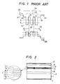
- Fig. 1 shows an energy band in a vicinity of a light emission region in the prior art semiconductor laser device.
- a light emission region laser 23 has a MQW structure having well layers 22 and barrier layers 21 alternately laminated. Clad layers 20 are provided on the opposite sides of the light emission region 23 and the barrier layers 19 to form an optical wave guide structure 24.
- variable wavelength semiconductor laser element has the following problems.
- a semiconductor laser device as specified in claim 1, the preamble of which corresponds to JP-A-59 106 171.
- parameters are set such that a light gain of the light emission layer of a longer oscillation wavelength is positive in an oscillation wavelength of one of light emission layers of shorter oscillation wavelength when a current close to an oscillation threshold is applied to the light emission layers.
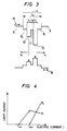
- Fig. 2 shows a sectional view of one embodiment of a semiconductor laser device of the present invention.
- Numeral 1 denotes an n-type GaAs substrate
- numeral 2 denotes an n-type GaAs buffer layer
- numeral 5 denotes an n-type AlGaAs clad layer
- numeral 4 denotes an optical wave guide structure
- numeral 3 denotes a p-type AlGaAs clad layer
- numeral 6 denotes a p-type GaAs cap layer
- numerals 7 and 8 denote electrodes.
- the optical wave guide structure 4 comprises a stack of a p-type AlGaAs barrier layer 92, a second non-doped AlGaAs light emission layer 12, a p-type AlGaAs barrier layer 11, a first non-doped GaAs light emission layer 10 and a p-type AlGaAs barrier layer 91, sequentially stacked on the clad layer 5.
- the clad layers 3 and 5 have lower refractive indexes than that of the optical wave guide structure 4 and function to confine the light emitted by the light emission layers in the structure 4.
- the device is fabricated by growing the various semiconductor layers having different energy gaps on the substrate 1 by a conventional semiconductor fabrication method, such as liquid phase epitaxy (LPE) method, organic metal vapor phase growth (MO-CVD) method or molecular beam epitaxy (MBE) method.
- LPE liquid phase epitaxy
- MO-CVD organic metal vapor phase growth
- MBE molecular beam epitaxy
- a laser resonance plane is formed by cleaving the semiconductor stack.
- a striped active region may be formed by restricting a current injection area parallelly to the resonance plane by known means such as a current restriction layer.
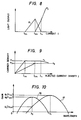
- Fig. 3 shows an energy band in a vicinity of the optical wave guide structure of the device shown in Fig. 2.
- the like elements to those shown in Fig. 2 are designated by the like numerals and detailed explanation thereof is omitted.
- the first light emission layer 10 has a narrower band gap than the second light emission layer 12.
- the buffer layers 91, 92 and 11 have wider band gaps than those of the light emission layers 10 and 12.
- a current-light output characteristic of the device is shown in Fig. 4, in which I denotes a current and P1 and P2 denote the output of the lights having the wavelengths ⁇ 1 and ⁇ 2, respectively.
- I a current
- P1 and P2 denote the output of the lights having the wavelengths ⁇ 1 and ⁇ 2, respectively.
- Fig. 7 shows an upper half of the energy band of the device of Fig. 2 and in which the like elements to those shown in Fig. 3 are designated by the like numerals and explanation thereof is omitted.
- n1 and n2 represent carrier densities in the first light emission layer 10 and the second light emission layer 12, respectively, and j represents an injection current density.
- Carriers injected into the second light emission layer 12 are spontaneously emitted or recombine with no light emission at a rate r2, transfer to the first light emission layer 10 at a rate r21 and the remaining carriers recombine with induction emission.
- ⁇ 1 and ⁇ 2 are photon energies of the lights having the wavelengths ⁇ 1 and ⁇ 2, respectively
- S1 and S2 are beam widths of the lights having the wavelengths ⁇ 1 and ⁇ 2, respectively
- ⁇ 1 and g1(n1) are confine coefficient and gain of the light having the wavelength ⁇ 1 in the first light emission layer
- ⁇ 2 and g2(n2) are confine coefficient and gain of the light having the wavelength ⁇ 2 in the second light emission layer
- ⁇ '2 and g'(n1) are confine coefficient and gain of the light having the wavelength ⁇ 2 in the first light emission layer
- L1 and L2 are thickness of the first light emission layer and the second light emission layer, respectively.
- Fig. 6 shows a gain distribution of the semiconductor laser device of the present invention when j 2th ⁇ j .
- Numerals 17 and 16 denote light gains of the first light emission layer 10 and the second light emission layer 12, respectively.
- the wavelengths ⁇ 1 and ⁇ 2 and the threshold currents I 1th and I 2th can be selected by the thickness of the first light emission layer 10, the second light emission layer 12 or the gap layer 11 and mixed crystal ratio and doping.
- the light having the wavelength ⁇ 1 and the light having the wavelength ⁇ 2 are both guided in the optical wave guide and those lights are emitted from the essentially same point on the end plane of the laser.
- the change of the wavelength in accordance with the present invention does not occur without condition.
- the operational condition thereof and specific design of the device are explained below.
- n 1th and j 1th are given as follows.
- Function forms of g1(n1) and g2(n2) depend on the structure of the active layer, and the function forms for the specific structure can be readily calculated or measured by using the method shown in "Semiconductor Laser and Light Integrated Circuit: edited by Suematsu, OHM Co. Ltd., 1984 or "Heterostructure Lasers", by Casey and Panish, Academic, 1978. Same is true for ⁇ 1, ⁇ 2, r1, r2, r21, ⁇ 1, ⁇ 2, ⁇ 2, ⁇ 1 and ⁇ 2. The results are put in the equations (17) et seq so that the condition for the desired characteristic is obtained.
- the g1(n1), g2(n2), ⁇ 1, ⁇ 2, ... are determined by the above method.
- the results are put in the equations (17) et seq and the operational condition for the variable wavelength laser (condition of the equation (19)) is checked and j 1th and j 2th are determined.
- specific x and L1, L2, ... for the variable wavelength laser for the desired characteristic are determined. Consequently, the semiconductor laser device can be fabricated as readily as the conventional semiconductor laser device is fabricated, by using MBE method, MO CVD method or LPE method.
- a method for controlling the magnitude of j 1th is specifically described.
- j 1th ' L1 may be reduced or r21 may be increased as seen from the equation (18).
- r21 a difference between band gaps of the barrier layer 11 and the second light emitting layer 12 may be reduced or the width L B of the barrier layer may be reduced.
- j 1th may be reduced by changing the width L G of the optical wave guide structure to increase ⁇ 1.
- the reversal of the above is carried out.
- the semiconductor laser device of the structure shown in Fig. 2 was fabricated by the molecule beam epitaxy method.
- An n-type GaAs buffer layer 2 having a thickness of 1 » m and an n-type (impurity concentration 5 x 1017 cm ⁇ 3) Al 0.7 Ga 0.3 As clad layer 5 having a thickness of 2 » m were grown on an n-type GaAs substrate 1.
- a barrier layer 92, a second light emission layer 12, a barrier layer 11, a first light emission layer 10 and a barrier layer 91 were sequentially grown on the clad layer 5.
- the first light emission layer 10 was a non-doped GaAs
- the second light emission layer 12 was a non-doped Al 0.1 Ga 0.9 As
- the barrier layers 91, 11 and 92 were p-type (impurity concentration 3 x 1018 cm ⁇ 3) Al 0.3 Ga 0.7 As.
- a p-type (impurity concentration 1 x 1018 cm ⁇ 3 ⁇ ) Al 0.7 Ga 0.3 As clad layer 3 having a thickness of 1.5 » m and a p-type GaAs cap layer 6 having a thickness of 0.5 » m were grown on the barrier layer 91.
- Portions of the cap layer 6 and the clad layer 3 were etched to a vicinity of the barrier layer 91 to form a striped recessed area, and an electrode 8 was vapor-deposited by using a dielectric mask so that it contacted only to the top of the non-etched cap layer 6.
- An electrode 7 was vapor-deposited to the buttom of the substrate 1. The laminated structure was cleaned to manufacture a semiconductor laser device having a laser resonance plane.
- a laser beam of a wavelength 870 nm was emitted, and at 120 mA, a laser beam of a wavelength 800 nm was additionally emitted.
- the semiconductor laser device having the switchable wavelength (the light having the wavelength ⁇ 1 is not generated when the light having the wavelength ⁇ 2 is generated) is obtained.
- Fig. 8 shows a current-light output characteristic of such device.
- I represents a current
- P1 and P2 represent light outputs of the wavelengths ⁇ 1 and ⁇ 2, respectively.
- I the current
- P1 and P2 represent light outputs of the wavelengths ⁇ 1 and ⁇ 2, respectively.
- I the current
- P1 and P2 represent light outputs of the wavelengths ⁇ 1 and ⁇ 2, respectively.
- I the current
- a principle of operation in the present example is similar to that explained with reference to Fig. 7, and rate equations therefor are given by the equations (1) and (2) as are done in the example of Fig. 4.
- Steady solutions of the rate equations are given in four regions. They are equal to the regions (i) to (iii) shown by the equations (3) - (12) until the light having the wavelength ⁇ 2 is generated.
- the region (iii) is defined in the range of j 2th ⁇ j ⁇ j 1V . There are following regions additionally.
- a change of the carrier density to the injection current density j is shown in Fig. 9.
- Fig. 10 shows a gain distribution of the semiconductor laser device of the present invention when I 2th ⁇ I ⁇ I 1V .
- Numerals 17 and 16 denote light gains of the first light emission layer 10 and the second light emission layer 12, respectively. If the light gain of the first light emission layer 10 is positive at the oscillation wavelength ⁇ 2 of the second light emission layer 12, the process (iv) takes place so that the switching between the wavelengths ⁇ 1 and ⁇ 2 is carried out.
- the ⁇ 1, ⁇ 2, I 1th , I 2th and I 1V may be set to any values by changing the thicknesses of the first light emission layer 10, the second light emission layer 12 and the gap layer 11, and the mixed crystal ratio and doping.
- a difference between the wavelengths ⁇ 1 and ⁇ 2 it is necessary that a wavelength range in which the light gain by the first light emission layer 10 is positive is wide in order to meet the condition of the equation (26).
- the width L1 of the first light emission layer may be narrowed.
- ⁇ is reduced and larger n1 is required for ⁇ 1g1(n1) to reach a level necessary for the laser oscillation, and n 1th increases.
- the wavelength region in which the gain is positive is widened.
- a semiconductor laser device of the structure shown in Fig. 2 was fabricated by the molecule beam epitaxy method.
- An n-type GaAs buffer layer 2 having a thickness of 1 » m and an n-type (impurity concentration 5 x 1017 cm ⁇ 3) Al 0.6 Ga 0.4 As clad layer 5 having a thickness of 2 » m were grown on an n-type GaAs substrate 1.
- a barrier layer 92, a second light emission layer 12, a barrier layer 11, a first light emission layer 10 and a barrier layer 91 were sequentially grown on the clad layer 5.
- the first light emission layer 10 was non-doped GaAs
- the second light emission layer 12 was non-doped Al 0.12 Ga 0.88 As
- the barrier layer 11 was p-type (impurity concentration 4 x 1018 cm ⁇ 3) Al 0.28 Ga 0.72 As
- the barrier layers 91 and 92 were p-type (impurity concentration 4 x 1018 cm ⁇ 3), Al 0.3 Ga 0.7 As.
- a p-type (impurity concentration 1 x 1018 cm ⁇ 3) Al 0.6 Ga 0.4 As clad layer 3 having a thickness of 1.5 » m and a p-type GaAs cap layer 6 having a thickness of 0.5 » m were grown on the barrier layer 91. Portions of the cap layer 6 and the clad layer 3 were etched to a vicinity of the barrier layer 91 to form a striped recessed area. It was then masked by a dielectric layer and an electrode 8 was vapor-deposited so that it contacted only to the top of the unetched cap layer 6. An electrode 7 was vapor-deposited on the bottom of the substrate 1. The lamination was cleaned to manufacture a semiconductor laser device having a laser resonance plane.
- a gradually increasing current was injected into the device.
- a laser beam having a wavelength of 830 nm was emitted, and at 85 mA, a laser beam having a wavelength of 780 nm was additionally emitted.
- the current was further increased, the light having the wavelength of 830 nm was stopped at 88 mA and only the laser beam having the wavelength of 780 nm was emitted.
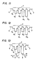
- a plurality of first light emission layers 101 and 102 and a plurality of second light emission layers 121 and 122 may be provided to increase the light output.
- a third light emission layer 18 for emitting a light having a wavelength ⁇ 3 may be provided to form a three-wavelength laser device.
- four or more-wavelength laser device may be formed.
- the AlGaAs system semiconductor laser device is shown in the embodiments, the present invention is applicable to a laser of any material such as InGaAsP system. The present invention includes all such modifications without departing from the scope of the claim.
- numerals 111, 112 and 113 denote barrier layers and the like elements to those shown in Fig. 2 are designated by the like numerals and detailed explanation thereof is omitted.
- a semiconductor substrate (1) In a semiconductor laser device for emitting a laser beam of a variable frequency depending on a current applied to the laser device, there are provided a semiconductor substrate (1), an optical waveguide structure (4) formed on the substrate having two or more semiconductor light emission layers (10, 12) and barrier layers (91, 92) having a wider band gap than that of the light emission layers, alternately stacked, clad layers (3, 5) stacked on the opposite sides of the waveguide structure and having a lower refractive index than that of the waveguide structure, and a device (7, 8) for applying a current to the light emission layers, and the wave guide structure includes at least first and the second light emission layers which respectively emit lights having different wavelengths.
Description
- The present invention relates to a semiconductor laser device, and more particularly to a semiconductor laser device which emits a laser beam of a variable frequency depending on a current applied to the device.
- Demands for a semiconductor laser device in a light communication field and a optical information processing field have been rapidly increasing and a requirement for the functions of the device is becoming versatile. A semiconductor laser device having a variable wavelength is one of the functions. For example, when information is to be recorded and reproduced by irradiating a laser beam to a medium such as an optical card or optical disk, writing by a reproduced light is prevented by setting an output of the reproduced light to be lower than a recording light. By setting the wavelength of the reproduced light to a low sensitivity area of the medium, the writing can be prevented without significantly reducing the output of the reproduced light and the information is reproduced with a high S/N ratio.
- For the above requirement, a variable wavelength semiconductor laser device which uses a high order quantum level of a multi-quantum well (MQW) has been proposed. Fig. 1 shows an energy band in a vicinity of a light emission region in the prior art semiconductor laser device. A light
emission region laser 23 has a MQW structure having welllayers 22 andbarrier layers 21 alternately laminated.Clad layers 20 are provided on the opposite sides of thelight emission region 23 and thebarrier layers 19 to form an opticalwave guide structure 24. When a current is injected to the semiconductor laser element,electrons 25 are stored at an energy level E₀ and recombine withholes 26 so that a light between quantum levels of n = 0 (n: principal quantum number) is generated (wavelength λ ₁). As the injection current increases, a carrier density of an energy level E₁ increases so that a light between quantum levels of n = 1 is generated (wavelength λ ₂) by recombination. In this manner, lights of different wavelengths are generated from one device. - However, the prior art variable wavelength semiconductor laser element has the following problems.
- (I) In order to generate lights of different wavelengths, it is necessary that absorption loss and mirror loss are significantly larger than normal, and hence the device efficiency is low.
- (II) Since different quantum levels are merely used, the difference between the generated wavelengths is several tens nm at most.
- (III) Since it is necessary to form a quantum well having two or more levels, one-level quantum well cannot be used even if such a device improves a characteristic.
- (IV) It is difficult to switch the wavelength.
(Namely, once a light of awavelength λ ₂ is generated, it is difficult to stop the generation of a light of a wavelength λ ₁). - It is an object of the present invention to provide a variable wavelength semiconductor laser device which has a wide variable wavelength range and operates at a high efficiency.
- It is another object of the present invention to provide a variable wavelength semiconductor laser device which permits easy switching of an oscillation wavelength.
- The above objects of the present invention are achieved by a semiconductor laser device as specified in
claim 1, the preamble of which corresponds to JP-A-59 106 171. In order to switch the wavelength in the device, parameters are set such that a light gain of the light emission layer of a longer oscillation wavelength is positive in an oscillation wavelength of one of light emission layers of shorter oscillation wavelength when a current close to an oscillation threshold is applied to the light emission layers. -
- Fig. 1 shows an energy band of a conventional variable wavelength semiconductor laser device.
- Fig. 2 shows a sectional view of one embodiment of the semiconductor laser element of the present invention.
- Fig. 3 shows an energy band of the device of Fig. 2.
- Fig. 4 shows a current-light output characteristic in the device of Fig. 2.
- Fig. 5 shows a change of a carrier density in light emission layers to an injection current density in the device of Fig. 2.
- Fig. 6 shows a light gain characteristic in the device of Fig. 2.
- Fig. 7 shows an energy band for illustrating a principle of operation of the device of Fig. 2.
- Fig. 8 shows a current-light output characteristic in another embodiment of the present invention.
- Fig. 9 shows a change of a carrier density in light emission layers to an injection current density in the other embodiment.
- Fig. 10 shows a light gain characteristic in the other embodiment, and
- Figs. 11 to 13 show energy bands of modifications of the present invention.
- Fig. 2 shows a sectional view of one embodiment of a semiconductor laser device of the present invention.
Numeral 1 denotes an n-type GaAs substrate,numeral 2 denotes an n-type GaAs buffer layer,numeral 5 denotes an n-type AlGaAs clad layer,numeral 4 denotes an optical wave guide structure,numeral 3 denotes a p-type AlGaAs clad layer, numeral 6 denotes a p-type GaAs cap layer andnumerals wave guide structure 4 comprises a stack of a p-typeAlGaAs barrier layer 9₂, a second non-doped AlGaAslight emission layer 12, a p-typeAlGaAs barrier layer 11, a first non-doped GaAslight emission layer 10 and a p-typeAlGaAs barrier layer 9₁, sequentially stacked on theclad layer 5. Theclad layers wave guide structure 4 and function to confine the light emitted by the light emission layers in thestructure 4. - The device is fabricated by growing the various semiconductor layers having different energy gaps on the
substrate 1 by a conventional semiconductor fabrication method, such as liquid phase epitaxy (LPE) method, organic metal vapor phase growth (MO-CVD) method or molecular beam epitaxy (MBE) method. A laser resonance plane is formed by cleaving the semiconductor stack. A striped active region may be formed by restricting a current injection area parallelly to the resonance plane by known means such as a current restriction layer. - Fig. 3 shows an energy band in a vicinity of the optical wave guide structure of the device shown in Fig. 2. The like elements to those shown in Fig. 2 are designated by the like numerals and detailed explanation thereof is omitted. As shown, the first
light emission layer 10 has a narrower band gap than the secondlight emission layer 12. Thebuffer layers light emission layers - When a current is applied to the
electrodes electrons 14 are injected to the firstlight emission layer 10 and the secondlight emission layer 12, and theelectrons 14 and theholes 15 in the firstlight emission layer 10 recombine to induce-emit a light having awavelength λ ₁. As the injection current is increased, the electrons and theholes 15 recombine in the secondlight emission layer 12, too, to induce-emit a light having awavelength λ ₂. - A current-light output characteristic of the device is shown in Fig. 4, in which I denotes a current and P₁ and P₂ denote the output of the lights having the
wavelengths λ ₁ andλ ₂, respectively. As the current I is increased, the light having thewavelength λ ₁ is generated at a first threshold current
wavelength λ ₂ is generated at a second threshold value
- A principle of operation of the semiconductor laser device of the present invention is explained with reference to Fig. 7, which shows an upper half of the energy band of the device of Fig. 2 and in which the like elements to those shown in Fig. 3 are designated by the like numerals and explanation thereof is omitted. In Fig. 7, n₁ and n₂ represent carrier densities in the first
light emission layer 10 and the secondlight emission layer 12, respectively, and j represents an injection current density. Carriers injected into the secondlight emission layer 12 are spontaneously emitted or recombine with no light emission at a rate r₂, transfer to the firstlight emission layer 10 at a rate r₂₁ and the remaining carriers recombine with induction emission. Further, the carriers transferred to the first light emission layer are spontaneously emitted or recombine with no light emission at a rate r₁ and the remaining carriers recombine with induction emission. Rate equations under this condition are expressed as follows (e (electron charge) = 1).
whereω₁ and ω₂ are photon energies of the lights having the
wavelengths λ ₁ andλ ₂, respectively, S₁ and S₂ are beam widths of the lights having thewavelengths λ ₁ andλ ₂, respectively,Γ ₁ and g₁(n₁) are confine coefficient and gain of the light having thewavelength λ ₁ in the firstlight emission layer 10,Γ ₂ and g₂(n₂) are confine coefficient and gain of the light having thewavelength λ ₂ in the secondlight emission layer 12, Γ'₂ and g'(n₁) are confine coefficient and gain of the light having thewavelength λ ₂ in the firstlight emission layer 10, and L₁ and L₂ are thickness of the first light emission layer and the second light emission layer, respectively. - Steady solutions of the above rate equations are obtained by the following three regions while taking saturation of the carrier density in the oscillation into account.
- (i)


- (ii)


- (iii)


- Fig. 6 shows a gain distribution of the semiconductor laser device of the present invention when

Numerals light emission layer 10 and the secondlight emission layer 12, respectively. - The
wavelengths λ ₁ andλ ₂ and the threshold currents I1th and I2th can be selected by the thickness of the firstlight emission layer 10, the secondlight emission layer 12 or thegap layer 11 and mixed crystal ratio and doping. - In the semiconductor laser device of the present invention, the light having the
wavelength λ ₁ and the light having the wavelength λ₂ are both guided in the optical wave guide and those lights are emitted from the essentially same point on the end plane of the laser. - The change of the wavelength in accordance with the present invention does not occur without condition. The operational condition thereof and specific design of the device are explained below.
- Laser oscillation conditions are shown below. When


oscillation condition for the light having the wavelength

oscillation condition for the light having the wavelength

where - α₁ :
- loss coefficient of the light having the
wavelength λ ₁ - α₂ :
- loss coefficient of the light having the
wavelength λ ₂ - L :
- length of a resonator of the semiconductor laser device
- R :
- (mean) reflection coefficient of an end plane of the resonator
- From the equations (4), (18) and (20), n1th and j1th are given as follows.

- From the equations (3), (14) and (16), the following condition is given.

- From the equations (5), (6), (14) and (16), n2th is given by

and j2th is given by

Function forms of g₁(n₁) and g₂(n₂) depend on the structure of the active layer, and the function forms for the specific structure can be readily calculated or measured by using the method shown in "Semiconductor Laser and Light Integrated Circuit: edited by Suematsu, OHM Co. Ltd., 1984 or "Heterostructure Lasers", by Casey and Panish, Academic, 1978. Same is true forλ ₁,λ ₂, r₁, r₂, r₂₁,Γ ₁,Γ ₂, Γʹ₂,α ₁ andα ₂. The results are put in the equations (17) et seq so that the condition for the desired characteristic is obtained. - For some combinations of x in the respective regions in Fig. 3 and the thickness L₁, L₂ LB and LG, the g₁(n₁), g₂(n₂),
λ ₁,λ ₂, ... are determined by the above method. The results are put in the equations (17) et seq and the operational condition for the variable wavelength laser (condition of the equation (19)) is checked and j1th and j2th are determined. Thus, specific x and L₁, L₂, ... for the variable wavelength laser for the desired characteristic are determined. Consequently, the semiconductor laser device can be fabricated as readily as the conventional semiconductor laser device is fabricated, by using MBE method, MO CVD method or LPE method. - As an example, a method for controlling the magnitude of j1th is specifically described. In order to reduce j1th' L₁ may be reduced or r₂₁ may be increased as seen from the equation (18). - In order to increase r₂₁, a difference between band gaps of the
barrier layer 11 and the secondlight emitting layer 12 may be reduced or the width LB of the barrier layer may be reduced. Further, j1th may be reduced by changing the width LG of the optical wave guide structure to increaseΓ ₁. On the other hand, in order to increase j1th, the reversal of the above is carried out. - Specific examples of the present invention are described below.
- The semiconductor laser device of the structure shown in Fig. 2 was fabricated by the molecule beam epitaxy method. An n-type
GaAs buffer layer 2 having a thickness of 1 » m and an n-type (impurity concentration 5 x 10¹⁷ cm⁻³) Al0.7Ga0.3As cladlayer 5 having a thickness of 2 » m were grown on an n-type GaAs substrate 1. Then, abarrier layer 9₂, a secondlight emission layer 12, abarrier layer 11, a firstlight emission layer 10 and abarrier layer 9₁ were sequentially grown on theclad layer 5. The firstlight emission layer 10 was a non-doped GaAs, the secondlight emission layer 12 was a non-doped Al0.1Ga0.9As and the barrier layers 9₁, 11 and 9₂ were p-type (impurity concentration 3 x 10¹⁸ cm⁻³) Al0.3Ga0.7As. The thicknesses of the layers were L₁ = 200 Å , L₂ = 200 Å, LB = 80 Å and LG = 0.1 » m in Fig. 3. A p-type (impurity concentration 1 x 10¹⁸ cm⁻³`) Al0.7Ga0.3As cladlayer 3 having a thickness of 1.5 » m and a p-type GaAs cap layer 6 having a thickness of 0.5 » m were grown on thebarrier layer 9₁. Portions of the cap layer 6 and theclad layer 3 were etched to a vicinity of thebarrier layer 9₁ to form a striped recessed area, and anelectrode 8 was vapor-deposited by using a dielectric mask so that it contacted only to the top of the non-etched cap layer 6. Anelectrode 7 was vapor-deposited to the buttom of thesubstrate 1. The laminated structure was cleaned to manufacture a semiconductor laser device having a laser resonance plane. - Gradually increasing current was applied to the device. At 110 mA, a laser beam of a wavelength 870 nm was emitted, and at 120 mA, a laser beam of a wavelength 800 nm was additionally emitted.
- In the present invention, if the device is designed such that when a current close to an oscillation threshold is applied to the device, a light gain of the light emission layer for the longer oscillation wavelength is positive at the oscillation wavelength of one of the light emission layers for shorter oscillation wavelength, then the semiconductor laser device having the switchable wavelength (the light having the
wavelength λ ₁ is not generated when the light having thewavelength λ ₂ is generated) is obtained. An example therefor is explained below. - Such a device is attained by appropriately selecting the materials of the light emission layers 10 and 12 in the structure of Fig. 2. Fig. 8 shows a current-light output characteristic of such device. In Fig. 8, I represents a current, and P₁ and P₂ represent light outputs of the
wavelengths λ ₁ andλ ₂, respectively. As the current I is increased, the light having thewavelength λ ₁ is generated at the first threshold current

wavelength λ ₂ is generated at the second threshold current
wavelength λ ₁ stops to oscillate at
wavelength λ ₂ is generated. Accordingly, by switching the injection current between a current which meets I1th < I < I2th and a current which meets I > I1V, the light having thewavelength λ ₁ and the light having thewavelength λ ₂ are selectively generated. - A principle of operation in the present example is similar to that explained with reference to Fig. 7, and rate equations therefor are given by the equations (1) and (2) as are done in the example of Fig. 4. Steady solutions of the rate equations are given in four regions. They are equal to the regions (i) to (iii) shown by the equations (3) - (12) until the light having the
wavelength λ ₂ is generated. The region (iii) is defined in the range of j2th ≦ j < j1V. There are following regions additionally. - (iv)


then P₁ decreases in the region of I2th ≦ I < I1V, and P₁ = 0 when I = I1V. Thus, the switching from thewavelength λ ₁ toλ ₂ is completed. - In order to facilitate understanding, a change of the carrier density to the injection current density j is shown in Fig. 9. The carrier density n₁ in the first light emission layer saturates at


- Fig. 10 shows a gain distribution of the semiconductor laser device of the present invention when I2th < I < I1V. Numerals 17 and 16 denote light gains of the first
light emission layer 10 and the secondlight emission layer 12, respectively. If the light gain of the firstlight emission layer 10 is positive at theoscillation wavelength λ ₂ of the secondlight emission layer 12, the process (iv) takes place so that the switching between thewavelengths λ ₁ andλ ₂ is carried out. - The
λ ₁,λ ₂, I1th, I2th and I1V may be set to any values by changing the thicknesses of the firstlight emission layer 10, the secondlight emission layer 12 and thegap layer 11, and the mixed crystal ratio and doping. When a difference between thewavelengths λ ₁ andλ ₂ is large, it is necessary that a wavelength range in which the light gain by the firstlight emission layer 10 is positive is wide in order to meet the condition of the equation (26). In this case, the width L₁ of the first light emission layer may be narrowed. As a result, Γ is reduced and larger n₁ is required for Γ₁g₁(n₁) to reach a level necessary for the laser oscillation, and n1th increases. As a result, the wavelength region in which the gain is positive is widened. - The operational condition in the present embodiment requires the followings in addition to the conditions shown by the equations (17) - (21).
- From the equation (12), the equation (26) is to be met.
- It is given by the equation (25).
- The design of the device in accordance with those conditions is done in the same manner as that for the embodiment of Fig. 4. An example is shown below.
- A semiconductor laser device of the structure shown in Fig. 2 was fabricated by the molecule beam epitaxy method. An n-type
GaAs buffer layer 2 having a thickness of 1 » m and an n-type (impurity concentration 5 x 10¹⁷ cm⁻³) Al0.6Ga0.4As cladlayer 5 having a thickness of 2 » m were grown on an n-type GaAs substrate 1. Then, abarrier layer 9₂, a secondlight emission layer 12, abarrier layer 11, a firstlight emission layer 10 and abarrier layer 9₁ were sequentially grown on theclad layer 5. The firstlight emission layer 10 was non-doped GaAs, the secondlight emission layer 12 was non-doped Al0.12Ga0.88As, thebarrier layer 11 was p-type (impurity concentration 4 x 10¹⁸ cm⁻³) Al0.28Ga0.72As, and the barrier layers 9₁ and 9₂ were p-type (impurity concentration 4 x 10¹⁸ cm⁻³), Al0.3Ga0.7As. The thicknesses of the layers were L₁ = 60 Å, L₂ = 120 Å, LB = 80 Å and LG = 0.2 » m in Fig. 2. A p-type (impurity concentration 1 x 10¹⁸ cm⁻³) Al0.6Ga0.4 As cladlayer 3 having a thickness of 1.5 » m and a p-type GaAs cap layer 6 having a thickness of 0.5 » m were grown on thebarrier layer 9₁. Portions of the cap layer 6 and theclad layer 3 were etched to a vicinity of thebarrier layer 9₁ to form a striped recessed area. It was then masked by a dielectric layer and anelectrode 8 was vapor-deposited so that it contacted only to the top of the unetched cap layer 6. Anelectrode 7 was vapor-deposited on the bottom of thesubstrate 1. The lamination was cleaned to manufacture a semiconductor laser device having a laser resonance plane. - A gradually increasing current was injected into the device. At 80 mA, a laser beam having a wavelength of 830 nm was emitted, and at 85 mA, a laser beam having a wavelength of 780 nm was additionally emitted. As the current was further increased, the light having the wavelength of 830 nm was stopped at 88 mA and only the laser beam having the wavelength of 780 nm was emitted.
- The present invention is not limited to the illustrated embodiments but various modifications thereof may be made. For example, as shown in Figs. 11 and 12, a plurality of first light emission layers 10₁ and 10₂ and a plurality of second light emission layers 12₁ and 12₂ may be provided to increase the light output. As shown in Fig. 13, a third
light emission layer 18 for emitting a light having a wavelength λ₃ may be provided to form a three-wavelength laser device. Similarly, four or more-wavelength laser device may be formed. While the AlGaAs system semiconductor laser device is shown in the embodiments, the present invention is applicable to a laser of any material such as InGaAsP system. The present invention includes all such modifications without departing from the scope of the claim. In Figs. 11 to 13,numerals - In a semiconductor laser device for emitting a laser beam of a variable frequency depending on a current applied to the laser device, there are provided a semiconductor substrate (1), an optical waveguide structure (4) formed on the substrate having two or more semiconductor light emission layers (10, 12) and barrier layers (91, 92) having a wider band gap than that of the light emission layers, alternately stacked, clad layers (3, 5) stacked on the opposite sides of the waveguide structure and having a lower refractive index than that of the waveguide structure, and a device (7, 8) for applying a current to the light emission layers, and the wave guide structure includes at least first and the second light emission layers which respectively emit lights having different wavelengths.
For easier understanding, a change of the carrier density to the injection current density j is shown in Fig. 5. A carrier density n₁ in the first light emission layer saturates at
From those, equations (17) et seq. are derived.
Claims (5)
- A semiconductor laser device comprising:
a semiconductor substrate (1);
an optical wave guide structure (4) formed on said substrate (1) and having two or more semiconductor light emission layers and barrier layers having a wider band gap than that of said light emission layers, alternately stacked;
said structure (4) including at least a first light emission layer (10) and a second light emission layer (12) which respectively emit lights having different wavelengths;
clad layers (3, 5) stacked on the opposite sides of said structure (4) and having a lower refractive index than that of said structure (4); and
means (7, 8) for applying a current to said semiconductor light emission layers, characterized in that
said first light emission layer (10) and second light emission layer (12) emit light having wavelenths λ ₁ and λ ₂, respectively, λ ₁ being longer than λ ₂ due to the bandgap of the first emission layer (10) being smaller than the bandgap of the second emission layer (12), and the following condition for variable wavelength depending on current is met
- A semiconductor laser device according to Claim 1, characterized in that
said optical wave guide structure (4) includes three or more semiconductor light emission layers (10, 12, 18) for emitting light of different wavelengths. - A semiconductor laser device according to Claim 1, characterized in that
said semiconductor substrate (1), said optical wave guide structure (4) and said clad layers (3, 5) are made of GaAs and AlGaAs. - A device according to Claim 1, characterized in that said first and second light emission layers (10, 12) are composed of non-doped semiconductors and an impurity is doped into said barrier layer(9₁, 9₂).
- A device according to Claim 1, characterized in that the optical gain of said first light emission layer (10) assumes positive at the wavelength λ₂ when a current in the vicinity of an oscillation threshold is applied to said device.
Applications Claiming Priority (4)
| Application Number | Priority Date | Filing Date | Title |
|---|---|---|---|
| JP44936/87 | 1987-02-27 | ||
| JP44939/87 | 1987-02-27 | ||
| JP62044939A JPH0728094B2 (en) | 1987-02-27 | 1987-02-27 | Semiconductor laser device |
| JP62044936A JPH0728093B2 (en) | 1987-02-27 | 1987-02-27 | Semiconductor laser device |
Publications (3)
| Publication Number | Publication Date |
|---|---|
| EP0280281A2 EP0280281A2 (en) | 1988-08-31 |
| EP0280281A3 EP0280281A3 (en) | 1989-03-08 |
| EP0280281B1 true EP0280281B1 (en) | 1994-06-15 |
Family
ID=26384901
Family Applications (1)
| Application Number | Title | Priority Date | Filing Date |
|---|---|---|---|
| EP88102756A Expired - Lifetime EP0280281B1 (en) | 1987-02-27 | 1988-02-24 | Variable oscillation wavelength semiconductor laser device |
Country Status (3)
| Country | Link |
|---|---|
| US (1) | US4982408A (en) |
| EP (1) | EP0280281B1 (en) |
| DE (1) | DE3850139T2 (en) |
Families Citing this family (16)
| Publication number | Priority date | Publication date | Assignee | Title |
|---|---|---|---|---|
| US5033053A (en) | 1989-03-30 | 1991-07-16 | Canon Kabushiki Kaisha | Semiconductor laser device having plurality of layers for emitting lights of different wavelengths and method of driving the same |
| US5138624A (en) * | 1989-11-16 | 1992-08-11 | The Boeing Company | Multiwavelength LED and laser diode optical source |
| US5124996A (en) * | 1990-03-02 | 1992-06-23 | Canon Kabushiki Kaisha | Semiconductor laser element having a plurality of layers emitting lights of different wavelengths, and its driving method |
| US5170289A (en) * | 1991-02-01 | 1992-12-08 | Grumman Aerospace Corporation | Optical correlator console |
| DE69222822T2 (en) * | 1991-09-06 | 1998-03-05 | Trw Inc | Optoelectronic switching device with quantum well structure and stimulated emission |
| US5200969A (en) * | 1991-10-18 | 1993-04-06 | Xerox Corporation | Switchable multiple wavelength semiconductor laser |
| US5214664A (en) * | 1991-10-18 | 1993-05-25 | Xerox Corporation | Multiple wavelength semiconductor laser |
| US5365535A (en) * | 1992-01-13 | 1994-11-15 | Canon Kabushiki Kaisha | Semiconductor laser and beam splitting devices, and optical information recording/reproducing, optical communication, and optomagnetic recording/reproducing apparatuses using semiconductor laser and beam splitting devices |
| FR2687011B1 (en) * | 1992-01-31 | 1994-07-08 | France Telecom | LOW SWITCHING TIME SEMICONDUCTOR OPTICAL AMPLIFIER. |
| US5384797A (en) * | 1992-09-21 | 1995-01-24 | Sdl, Inc. | Monolithic multi-wavelength laser diode array |
| US5436193A (en) * | 1993-11-02 | 1995-07-25 | Xerox Corporation | Method of fabricating a stacked active region laser array |
| US5386428A (en) * | 1993-11-02 | 1995-01-31 | Xerox Corporation | Stacked active region laser array for multicolor emissions |
| JPH07235732A (en) * | 1993-12-28 | 1995-09-05 | Nec Corp | Semiconductor laser |
| US5390209A (en) * | 1994-01-05 | 1995-02-14 | At&T Corp. | Article comprising a semiconductor laser that is non-degenerate with regard to polarization |
| US9564151B1 (en) | 2015-08-28 | 2017-02-07 | Seagate Technology Llc | Data writer coil heater |
| US10290994B2 (en) * | 2015-10-30 | 2019-05-14 | Canon Kabushiki Kaisha | Laser device, information acquisition device, and imaging system |
Family Cites Families (6)
| Publication number | Priority date | Publication date | Assignee | Title |
|---|---|---|---|---|
| JPS57190392A (en) * | 1981-05-20 | 1982-11-22 | Nippon Telegr & Teleph Corp <Ntt> | Semiconductor light-emitting device |
| JPH07112089B2 (en) * | 1982-12-07 | 1995-11-29 | 富士通株式会社 | Semiconductor light emitting device |
| JPH07112090B2 (en) * | 1982-12-10 | 1995-11-29 | 富士通株式会社 | Semiconductor light emitting device |
| US4602370A (en) * | 1983-05-12 | 1986-07-22 | At&T Bell Laboratories | Large optical cavity laser having a plurality of active layers |
| JPS61168983A (en) * | 1985-01-22 | 1986-07-30 | Nec Corp | High output semiconductor laser |
| DE3751548T2 (en) * | 1986-07-25 | 1996-04-11 | Mitsubishi Electric Corp | Semiconductor laser. |
-
1988
- 1988-02-24 DE DE3850139T patent/DE3850139T2/en not_active Expired - Lifetime
- 1988-02-24 EP EP88102756A patent/EP0280281B1/en not_active Expired - Lifetime
-
1990
- 1990-04-16 US US07/511,921 patent/US4982408A/en not_active Expired - Lifetime
Also Published As
| Publication number | Publication date |
|---|---|
| US4982408A (en) | 1991-01-01 |
| EP0280281A2 (en) | 1988-08-31 |
| EP0280281A3 (en) | 1989-03-08 |
| DE3850139D1 (en) | 1994-07-21 |
| DE3850139T2 (en) | 1994-10-06 |
Similar Documents
| Publication | Publication Date | Title |
|---|---|---|
| EP0547044B1 (en) | A semiconductor laser device | |
| JP3504742B2 (en) | Laser diode | |
| EP0280281B1 (en) | Variable oscillation wavelength semiconductor laser device | |
| US5353295A (en) | Semiconductor laser device with coupled cavities | |
| US4750183A (en) | Semiconductor laser device | |
| US5289484A (en) | Laser diode | |
| US4823352A (en) | Semiconductor laser with a variable oscillation wavelength | |
| JPH0143472B2 (en) | ||
| EP0579244A2 (en) | A semiconductor laser and a method for producing the same | |
| US4905246A (en) | Semiconductor laser device | |
| US6487225B2 (en) | Surface-emitting laser device | |
| Dutta et al. | Linewidth enhancement factor in strained quantum well lasers | |
| US6846685B2 (en) | Vertical-cavity surface-emitting semiconductor laser | |
| US4745615A (en) | Semiconductor laser device with a diffraction grating | |
| JPH09167873A (en) | Semiconductor laser device | |
| US4745616A (en) | Semiconductor laser device with a diffraction grating | |
| US5304507A (en) | Process for manufacturing semiconductor laser having low oscillation threshold current | |
| EP0284684B1 (en) | Inverted channel substrate planar semiconductor laser | |
| JPH04350988A (en) | Light-emitting element of quantum well structure | |
| JP2748570B2 (en) | Semiconductor laser device | |
| JPH06188513A (en) | Semiconductor laser and fabrication thereof | |
| JPH0728093B2 (en) | Semiconductor laser device | |
| JP3204969B2 (en) | Semiconductor laser and optical communication system | |
| JPH0278290A (en) | Semiconductor laser device | |
| JP2794743B2 (en) | Quantum well semiconductor laser device |
Legal Events
| Date | Code | Title | Description |
|---|---|---|---|
| PUAI | Public reference made under article 153(3) epc to a published international application that has entered the european phase |
Free format text: ORIGINAL CODE: 0009012 |
|
| AK | Designated contracting states |
Kind code of ref document: A2 Designated state(s): DE FR GB |
|
| PUAL | Search report despatched |
Free format text: ORIGINAL CODE: 0009013 |
|
| AK | Designated contracting states |
Kind code of ref document: A3 Designated state(s): DE FR GB |
|
| 17P | Request for examination filed |
Effective date: 19890721 |
|
| 17Q | First examination report despatched |
Effective date: 19920318 |
|
| GRAA | (expected) grant |
Free format text: ORIGINAL CODE: 0009210 |
|
| AK | Designated contracting states |
Kind code of ref document: B1 Designated state(s): DE FR GB |
|
| REF | Corresponds to: |
Ref document number: 3850139 Country of ref document: DE Date of ref document: 19940721 |
|
| ET | Fr: translation filed | ||
| PLBE | No opposition filed within time limit |
Free format text: ORIGINAL CODE: 0009261 |
|
| STAA | Information on the status of an ep patent application or granted ep patent |
Free format text: STATUS: NO OPPOSITION FILED WITHIN TIME LIMIT |
|
| 26N | No opposition filed | ||
| REG | Reference to a national code |
Ref country code: GB Ref legal event code: IF02 |
|
| PGFP | Annual fee paid to national office [announced via postgrant information from national office to epo] |
Ref country code: GB Payment date: 20070221 Year of fee payment: 20 |
|
| PGFP | Annual fee paid to national office [announced via postgrant information from national office to epo] |
Ref country code: DE Payment date: 20070222 Year of fee payment: 20 |
|
| REG | Reference to a national code |
Ref country code: GB Ref legal event code: PE20 |
|
| PGFP | Annual fee paid to national office [announced via postgrant information from national office to epo] |
Ref country code: FR Payment date: 20070208 Year of fee payment: 20 |
|
| PG25 | Lapsed in a contracting state [announced via postgrant information from national office to epo] |
Ref country code: GB Free format text: LAPSE BECAUSE OF EXPIRATION OF PROTECTION Effective date: 20080223 |