EP0282926A2 - ID system and method of writing data in an ID system - Google Patents
ID system and method of writing data in an ID system Download PDFInfo
- Publication number
- EP0282926A2 EP0282926A2 EP88103904A EP88103904A EP0282926A2 EP 0282926 A2 EP0282926 A2 EP 0282926A2 EP 88103904 A EP88103904 A EP 88103904A EP 88103904 A EP88103904 A EP 88103904A EP 0282926 A2 EP0282926 A2 EP 0282926A2
- Authority
- EP
- European Patent Office
- Prior art keywords
- data
- memory
- controller
- write
- storage means
- Prior art date
- Legal status (The legal status is an assumption and is not a legal conclusion. Google has not performed a legal analysis and makes no representation as to the accuracy of the status listed.)
- Granted
Links
Images


Classifications
-
- G—PHYSICS
- G06—COMPUTING; CALCULATING OR COUNTING
- G06K—GRAPHICAL DATA READING; PRESENTATION OF DATA; RECORD CARRIERS; HANDLING RECORD CARRIERS
- G06K19/00—Record carriers for use with machines and with at least a part designed to carry digital markings
- G06K19/06—Record carriers for use with machines and with at least a part designed to carry digital markings characterised by the kind of the digital marking, e.g. shape, nature, code
- G06K19/067—Record carriers with conductive marks, printed circuits or semiconductor circuit elements, e.g. credit or identity cards also with resonating or responding marks without active components
- G06K19/07—Record carriers with conductive marks, printed circuits or semiconductor circuit elements, e.g. credit or identity cards also with resonating or responding marks without active components with integrated circuit chips
- G06K19/0723—Record carriers with conductive marks, printed circuits or semiconductor circuit elements, e.g. credit or identity cards also with resonating or responding marks without active components with integrated circuit chips the record carrier comprising an arrangement for non-contact communication, e.g. wireless communication circuits on transponder cards, non-contact smart cards or RFIDs
-
- G—PHYSICS
- G06—COMPUTING; CALCULATING OR COUNTING
- G06K—GRAPHICAL DATA READING; PRESENTATION OF DATA; RECORD CARRIERS; HANDLING RECORD CARRIERS
- G06K7/00—Methods or arrangements for sensing record carriers, e.g. for reading patterns
- G06K7/0008—General problems related to the reading of electronic memory record carriers, independent of its reading method, e.g. power transfer
Definitions
- This invention relates to a method of writing data in an ID (identification) system in which, under the control of a host computer, data from a second device such as an ID controller or the like is transmitted via transmission means to a first device such as a data carrier which includes a memory such as an EE PROM (electrically erasable programmable read-only memory) and is written in the memory, or data is read out of the memory and is transmitted from the first device to the second device via the transmission means.
- a first device such as a data carrier which includes a memory such as an EE PROM (electrically erasable programmable read-only memory) and is written in the memory, or data is read out of the memory and is transmitted from the first device to the second device via the transmission means.
- EE PROM electrically erasable programmable read-only memory
- ID systems are available for identifying the types of assembly parts, manufactured parts, semi-fabricated products delivered on a conveyor or the type of tool on a machine tool, by way of example.
- One type of such an ID system which has recently been considered employs data carrier elements affixed to these articles.
- Each data carrier contains a memory in which specific data from a controller can be written or from which data can be read.
- each data carrier is assigned an identification code indicative of the article, tool or the like to which the carrier is attached, and extremely important data is stored in the memory of the data carrier.
- data may relate to the length, diameter and offset of a tool, the cumulative utilization time thereof, tool lifetime, amount of wear, etc. Destruction of these data must be avoided at all cost.
- sufficient care must be taken to avoid erasing the old data stored in the memory. For example, if a data storage area is mistakenly addressed or if a write error occurs, the old data will be lost and cannot be restored. Above all, if the data is data relating to the total utilization time of a tool, such old data is impossible to recover once lost.
- An object of the present invention is to provide a method and apparatus through which old data stored in the memory of a data carrier can be readily reproduced when an error occurs in the writing of new data in the memory.
- a method of writing data in an ID system comprising a first device having an electrically readable/writable memory for holding data and attached to an article to be identified, and a second device capable of contactless communication with the first device, wherein the first device is provided with first and second temporary storage means in addition to the electrically readable/writable memory, the method comprising the following steps in the first device: receiving a write command and write data from the second device and, in response thereto, storing the received write data in the first temporary storage means, reading data out of the memory from a location thereof in which the write data is to be written and storing this read data in the second temporary storage means, and thereafter writing the write data stored in the first temporary storage means in the aforementioned location of the memory; and the following steps in the second device: sending a read command to the first device after sending the write command, thereby causing the data written in the memory by the foregoing write processing to be read out, receiving this read data, comparing this received data with write data preserved in the second
- An ID system in accordance with the present invention comprises a data carrier attached to an article to be identified, and an ID controller capable of communicating with the data carrier;
- the data carrier comprising: a data readable/writable memory, first and second temporary storage means, means responsive to a write command from the ID controller for storing write data received together with the write command in the first temporary storage means, reading old data out of the memory from a location thereof in which the write data is to be written and storing this old data in the second temporary storage means, and storing the stored data of the first temporary storage means in the aforementioned location of the memory, means responsive to a first read command from the ID controller for reading the data written in the memory by the foregoing processing out of the memory and sending the data to the ID controller, and means responsive to a second read command from the ID controller for reading out the old data stored in the second storate means and sending the old data to the ID controller; and the ID controller comprises: means for comparing the data sent from the data carrier responsive to the first read command with the write data held in the ID
- the first device namely the data carrier
- the first and second temporary storage means in addition to the memory.
- Data (new data) from the second device, namely the ID controller, sent to the data carrier to be written in the memory thereof is stored in the first storage means.
- Old data stored at a location of the memory where the new data is to be written is read out and preserved in the second temporary storage means. Accordingly, even if an error is made in the writing of the new data, the old data is preserved in the second temporary storage means and, hence, the recovery of the old data is possible.
- the old data in the second temporary storage means is sent to the ID controller and is stored in the ID controller or in a host computer which controls the ID controller.
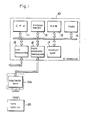
- Fig. 1 is a block diagram illustrating an ID system embodying the present embodiment.
- the ID system includes an ID controller 10 having a read/write head 10a, and a data carrier 20 supplied with electric power electromagnetically via the read/write head 10a and adapted to exchange data with the ID controller 10 electromagnetically via the head 10a.
- the ID controller 10 includes a CPU 11, a program memory 12, a RAM 13, a timer 14 for timekeeping purposes, a host transmitter 15 for being connected to a host computer, a slave modulator/demodulator circuit 16 for exchanging commands and data with the data carrier 20 on the slave side, and display lamps 17 for displaying the status of operation.
- the ID controller 10 executes control for converting commands, data and the like from the host computer into commands, data and the like in a form capable of being transmitted to the data carrier 20 on the slave side.
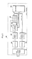
- Fig. 2 is a block diagram illustrating the detailed construction of the data carrier 20.
- the data carrier 20 includes a modulator/demodulator circuit 21 electromagnetically coupled to the read/write head 10a of the ID controller 10, a decoding circuit 22 for decoding a signal received from the modulator/demodulator circuit 21, a serial input circuit 23, a command decoder 24 for decoding a command applied thereto, a data buffer 25, an EE PROM 26 in which data to be stored is written or from which data is read, a serial output circuit 27 used when data are read out of the EE PROM 26, and an encoding circuit 28 for encoding data to be transmitted before applying the data to the modulator/demodulator circuit 21.
- the data buffer 25 includes two RAM areas 25a (first temporary storage means) and 25b (second temporary storage means), each of which has a storage area for storing one page (eight bytes) of data in the EE PROM 26.
- Various data is written in and read from the EE PROM 26 in page units of eight bytes.
- the data carrier 20 does not possess an internal power supply circuit but is supplied with its operating power electromagnetically in contactless fashion from the ID controller 10 via the modulator/demodulator circuit 21.
- the power supply circuit of the ID controller 10 is not shown in the drawings.
- Fig. 3 is an external view of the ID system of the illustrated embodiment.
- the read/write head 10a and the ID controller 10 are connected by a lead wire 10b.
- the data carrier 20 is composed of a single chip and is attached to an assembly part conveyed on a conveyor, a tool on a machine tool or a tool for an automatic tool changing apparatus or the like.
- data carrier 20 approaches or passes by the read/write head 10a during the conveyance of the article or tool, data is written in the data carrier 20 via the read/write head 10a or data from the data carrier 20 is read out to the ID controller 10 and host equipment via the read/write head 10a, this being performed under the control of the ID controller 10.
- Fig. 4 illustrates commands and the like from the host computer
- the central column indicates processing performed by the ID controller 10
- the right column shows the processing performed by the data carrier 20.
- a write command from the host computer is sent to the ID controller at a step ST1.
- the write command is composed of a command code, the starting address of the location of the EE PROM 26 at which data is to be written, and the write data (new data) to be written.
- the write command is preserved in the RAM 13 of the ID controller 10 for subsequent comparison processing.
- the write command is also transmitted to the data carrier 20 at a step ST2.
- the received command is decoded on the side of the data carrier 20, where the write data contained in the write command is stored in the first buffer 25a.
- the old data in the EE PROM 26 at the location where the write data is to be written is read out of the EE PROM 26 and stored in the second buffer 25b. Thereafter, the data stored in the first buffer 25a is written in the aforementioned location of the EE PROM 26 at a step ST3.
- the EE PROM 26 is adapted to store eight bytes in the form of one page and is written in page units at the time of a write operation. Accordingly, the old data read out of the one-page, eight-byte EE PROM 26 including the location in which the write data is to be written is actually stored in the second buffer 25b. Furthermore, in the first buffer 25a, prescribed data contained in the old data read out of the one-page, eight-byte EE PROM 26 is replaced by the new data and this eight-byte data is written collectively in the EE PROM.
- the data carrier 20 sends a write response indicative of the end of the write operation back to the ID controller 10 at a step ST4.
- the ID controller 10 next transmits a read command to the ID controller 10 at a step ST5.
- the data carrier 20 reads the new write data, which was written in the EE EPROM 26 at the step ST3, out of the EE PROM at a step ST6, and transmits a read response to the ID controller 10 together with the new write data just read at a step ST7.
- the write command inclusive of the new write data transmitted by the host computer has already been stored in the RAM 13 of the ID controller 10.
- the ID controller 10 now proceeds to compare the write data already stored in the RAM 13 prior to the write operation with the read data containing the read response from the data carrier 20 at a step ST8. If the compared data agree, the write operation is construed as being correct and the ID controller 10 transmits a write response to the host computer at a step ST9. If the compared data are found not to agree at the step ST8, on the other hand, namely if the write operation was not performed correctly, the ID controller 10 sends a data read command to the data carrier 20 at a step ST10.
- the data carrier 20 Upon receiving the data read command, the data carrier 20 first reads one page of the old data, which has been read out of the EE PROM 26 and stored in the second buffer 25b, out of the second buffer 25b at a step ST11 and then sends this data back to the ID controller 10 together with the data read response at a step ST12.
- the ID controller 10 sends this data read response from the data carrier 20 back to the host computer as a write response at a step ST13.
- the data carrier 20 is supplied with operating power only when it approaches the head 10a and is cut off from such power when it departs from the head 10a.
- the data buffer 25b is of the volatile type requiring a back-up power supply
- the old data stored in the buffer 25b is erased when the the supply of power is cut off.
- the old data is sent from the data carrier 20 to the host computer via the ID controller 10, and the data is preserved in the host computer.
- the host computer In a case where the host computer receives the write response together with the old data, the host computer construes this as meaning that the write operation just attempted was not performed normally and executes suitable processing, such as writing the data again at the same or a different address of the EE PROM 26 in data carrier 20.
- the old data is the cumulative utilization time of a tool, for example, writing the old data in the data carrier 20 again is very meaningful. Specifically, cumulative utilization time is data which grows larger in successive fashion, so that there is very little difference between the immediately preceding item of this old data and the current item of new data. Accordingly, the old data can be written in the data carrier 20 in place of the current item of new data and can be treated as effective data without leading to substantial difficulties.
- the above-described outstanding effects can be achieved with little additional hardware, it being sufficent to add only the second data buffer 25b to the data carrier 20 in order to store data temporarily.
- the ID controller 10 communicates with the data carrier 20 under the control of a host computer in the illustrated embodiment, the host computer is not absolutely essential and can be deleted.
Abstract
Description
- This invention relates to a method of writing data in an ID (identification) system in which, under the control of a host computer, data from a second device such as an ID controller or the like is transmitted via transmission means to a first device such as a data carrier which includes a memory such as an EE PROM (electrically erasable programmable read-only memory) and is written in the memory, or data is read out of the memory and is transmitted from the first device to the second device via the transmission means.
- ID systems are available for identifying the types of assembly parts, manufactured parts, semi-fabricated products delivered on a conveyor or the type of tool on a machine tool, by way of example. One type of such an ID system which has recently been considered employs data carrier elements affixed to these articles. Each data carrier contains a memory in which specific data from a controller can be written or from which data can be read.
- In this conventonal ID system, each data carrier is assigned an identification code indicative of the article, tool or the like to which the carrier is attached, and extremely important data is stored in the memory of the data carrier. For instance, such data may relate to the length, diameter and offset of a tool, the cumulative utilization time thereof, tool lifetime, amount of wear, etc. Destruction of these data must be avoided at all cost. In particular, in the execution of processing for writing new data in the memory, sufficient care must be taken to avoid erasing the old data stored in the memory. For example, if a data storage area is mistakenly addressed or if a write error occurs, the old data will be lost and cannot be restored. Above all, if the data is data relating to the total utilization time of a tool, such old data is impossible to recover once lost.
- An object of the present invention is to provide a method and apparatus through which old data stored in the memory of a data carrier can be readily reproduced when an error occurs in the writing of new data in the memory.
- In accordance with the present invention, a method of writing data in an ID system comprising a first device having an electrically readable/writable memory for holding data and attached to an article to be identified, and a second device capable of contactless communication with the first device, wherein the first device is provided with first and second temporary storage means in addition to the electrically readable/writable memory, the method comprising the following steps in the first device: receiving a write command and write data from the second device and, in response thereto, storing the received write data in the first temporary storage means, reading data out of the memory from a location thereof in which the write data is to be written and storing this read data in the second temporary storage means, and thereafter writing the write data stored in the first temporary storage means in the aforementioned location of the memory; and the following steps in the second device: sending a read command to the first device after sending the write command, thereby causing the data written in the memory by the foregoing write processing to be read out, receiving this read data, comparing this received data with write data preserved in the second device, outputting a normal write response if the two items of compared data agree, causing the first device to send the data stored in the second temporary storage means thereof to the second device if the two compared items of data fail to agree, and outputting the data of the second temporary storage means together with a response indicating non-agreement of the compared data.
- An ID system in accordance with the present invention comprises a data carrier attached to an article to be identified, and an ID controller capable of communicating with the data carrier; the data carrier comprising: a data readable/writable memory, first and second temporary storage means, means responsive to a write command from the ID controller for storing write data received together with the write command in the first temporary storage means, reading old data out of the memory from a location thereof in which the write data is to be written and storing this old data in the second temporary storage means, and storing the stored data of the first temporary storage means in the aforementioned location of the memory, means responsive to a first read command from the ID controller for reading the data written in the memory by the foregoing processing out of the memory and sending the data to the ID controller, and means responsive to a second read command from the ID controller for reading out the old data stored in the second storate means and sending the old data to the ID controller; and the ID controller comprises: means for comparing the data sent from the data carrier responsive to the first read command with the write data held in the ID controller, and means for sending the second read command to the data carrier if the comparison indicates that the two compared items of data fail to agree.
- Thus, in accordance with the invention, the first device, namely the data carrier, is provided with the first and second temporary storage means in addition to the memory. Data (new data) from the second device, namely the ID controller, sent to the data carrier to be written in the memory thereof is stored in the first storage means. Old data stored at a location of the memory where the new data is to be written is read out and preserved in the second temporary storage means. Accordingly, even if an error is made in the writing of the new data, the old data is preserved in the second temporary storage means and, hence, the recovery of the old data is possible. The old data in the second temporary storage means is sent to the ID controller and is stored in the ID controller or in a host computer which controls the ID controller. Thus, whenever necessary, old data can be written in the memory of a data carrier, old data can be written in the memory of another data carrier, or a host computer can execute processing using the old data.
- Other features and advantages of the present invention will be apparent from the following description taken in conjunction with the accompanying drawings.
-
- Fig. 1 is a block diagram illustrating the construction of an ID system, particularly an ID controller;
- Fig. 2 is a block diagram illustrating the construction of a data carrier;
- Fig. 3 is a perspective illustrating an example of the external appearance of an ID system; and
- Fig. 4 is a flowchart illustrating a data write operation in the ID system.
- An embodiment of the present invention will now be described in detail with reference to the drawings.
- Fig. 1 is a block diagram illustrating an ID system embodying the present embodiment.
- The ID system includes an
ID controller 10 having a read/writehead 10a, and adata carrier 20 supplied with electric power electromagnetically via the read/writehead 10a and adapted to exchange data with theID controller 10 electromagnetically via thehead 10a. - The
ID controller 10 includes a CPU 11, aprogram memory 12, aRAM 13, atimer 14 for timekeeping purposes, ahost transmitter 15 for being connected to a host computer, a slave modulator/demodulator circuit 16 for exchanging commands and data with thedata carrier 20 on the slave side, and displaylamps 17 for displaying the status of operation. TheID controller 10 executes control for converting commands, data and the like from the host computer into commands, data and the like in a form capable of being transmitted to thedata carrier 20 on the slave side. - Fig. 2 is a block diagram illustrating the detailed construction of the
data carrier 20. Thedata carrier 20 includes a modulator/demodulator circuit 21 electromagnetically coupled to the read/writehead 10a of theID controller 10, adecoding circuit 22 for decoding a signal received from the modulator/demodulator circuit 21, aserial input circuit 23, acommand decoder 24 for decoding a command applied thereto, adata buffer 25, anEE PROM 26 in which data to be stored is written or from which data is read, aserial output circuit 27 used when data are read out of theEE PROM 26, and anencoding circuit 28 for encoding data to be transmitted before applying the data to the modulator/demodulator circuit 21. Thedata buffer 25 includes two RAM areas 25a (first temporary storage means) and 25b (second temporary storage means), each of which has a storage area for storing one page (eight bytes) of data in theEE PROM 26. Various data is written in and read from the EEPROM 26 in page units of eight bytes. Thedata carrier 20 does not possess an internal power supply circuit but is supplied with its operating power electromagnetically in contactless fashion from theID controller 10 via the modulator/demodulator circuit 21. The power supply circuit of theID controller 10 is not shown in the drawings. - Fig. 3 is an external view of the ID system of the illustrated embodiment. The read/write
head 10a and theID controller 10 are connected by a lead wire 10b. Thedata carrier 20 is composed of a single chip and is attached to an assembly part conveyed on a conveyor, a tool on a machine tool or a tool for an automatic tool changing apparatus or the like. When thedata carrier 20 approaches or passes by the read/writehead 10a during the conveyance of the article or tool, data is written in thedata carrier 20 via the read/writehead 10a or data from thedata carrier 20 is read out to theID controller 10 and host equipment via the read/writehead 10a, this being performed under the control of theID controller 10. - The operation for writing data from the ID controller to the data carrier in the ID system of this embodiment will now be described with reference to the flowchart of Fig. 4. The left column in Fig. 4 illustrates commands and the like from the host computer, the central column indicates processing performed by the
ID controller 10, and the right column shows the processing performed by thedata carrier 20. - First, a write command from the host computer is sent to the ID controller at a step ST1. The write command is composed of a command code, the starting address of the location of the EE
PROM 26 at which data is to be written, and the write data (new data) to be written. The write command is preserved in theRAM 13 of theID controller 10 for subsequent comparison processing. The write command is also transmitted to thedata carrier 20 at a step ST2. The received command is decoded on the side of thedata carrier 20, where the write data contained in the write command is stored in the first buffer 25a. The old data in the EEPROM 26 at the location where the write data is to be written is read out of theEE PROM 26 and stored in thesecond buffer 25b. Thereafter, the data stored in the first buffer 25a is written in the aforementioned location of the EEPROM 26 at a step ST3. - Ordinarily, the EE
PROM 26 is adapted to store eight bytes in the form of one page and is written in page units at the time of a write operation. Accordingly, the old data read out of the one-page, eight-byte EE PROM 26 including the location in which the write data is to be written is actually stored in thesecond buffer 25b. Furthermore, in the first buffer 25a, prescribed data contained in the old data read out of the one-page, eight-byte EE PROM 26 is replaced by the new data and this eight-byte data is written collectively in the EE PROM. - In accordance with the invention however, it will suffice if new write data sent by the ID controller is rewritten in memory. Therefore, it will suffice if the old data (even one word) that is to be written by the new write data is stored in the
second buffer 25b. - When the writting of the new write data in the EE
PROM 26 ends, thedata carrier 20 sends a write response indicative of the end of the write operation back to theID controller 10 at a step ST4. Upon receiving the write response, theID controller 10 next transmits a read command to theID controller 10 at a step ST5. Upon receiving the read command, thedata carrier 20 reads the new write data, which was written in theEE EPROM 26 at the step ST3, out of the EE PROM at a step ST6, and transmits a read response to theID controller 10 together with the new write data just read at a step ST7. As mentioned above, the write command inclusive of the new write data transmitted by the host computer has already been stored in theRAM 13 of theID controller 10. TheID controller 10 now proceeds to compare the write data already stored in theRAM 13 prior to the write operation with the read data containing the read response from thedata carrier 20 at a step ST8. If the compared data agree, the write operation is construed as being correct and theID controller 10 transmits a write response to the host computer at a step ST9. If the compared data are found not to agree at the step ST8, on the other hand, namely if the write operation was not performed correctly, theID controller 10 sends a data read command to thedata carrier 20 at a step ST10. - Upon receiving the data read command, the
data carrier 20 first reads one page of the old data, which has been read out of theEE PROM 26 and stored in thesecond buffer 25b, out of thesecond buffer 25b at a step ST11 and then sends this data back to theID controller 10 together with the data read response at a step ST12. TheID controller 10 sends this data read response from thedata carrier 20 back to the host computer as a write response at a step ST13. - Thus, as set forth above, the
data carrier 20 is supplied with operating power only when it approaches thehead 10a and is cut off from such power when it departs from thehead 10a. In a case where thedata buffer 25b is of the volatile type requiring a back-up power supply, the old data stored in thebuffer 25b is erased when the the supply of power is cut off. In order to prevent this from occurring, the old data is sent from thedata carrier 20 to the host computer via theID controller 10, and the data is preserved in the host computer. - In a case where the host computer receives the write response together with the old data, the host computer construes this as meaning that the write operation just attempted was not performed normally and executes suitable processing, such as writing the data again at the same or a different address of the
EE PROM 26 indata carrier 20. If the old data is the cumulative utilization time of a tool, for example, writing the old data in thedata carrier 20 again is very meaningful. Specifically, cumulative utilization time is data which grows larger in successive fashion, so that there is very little difference between the immediately preceding item of this old data and the current item of new data. Accordingly, the old data can be written in thedata carrier 20 in place of the current item of new data and can be treated as effective data without leading to substantial difficulties. - In accordance with the ID system of the present embodiment, the above-described outstanding effects can be achieved with little additional hardware, it being sufficent to add only the
second data buffer 25b to thedata carrier 20 in order to store data temporarily. - Though the
ID controller 10 communicates with thedata carrier 20 under the control of a host computer in the illustrated embodiment, the host computer is not absolutely essential and can be deleted. - As many apparently widely different embodiments of the present invention can be made without departing from the spirit and scope thereof, it is to be understood that the invention is not limited to the specific embodiments thereof except as defined in the appended claims.
Claims (3)
receiving a write command and write data from said second device (10) and, in response thereto, storing the received write data in said first temporary storage means (25a);
reading data out of said memory (26) from a location thereof in which the write data is to be written and storing this read data in said second temporary storage means (25b); and
thereafter writing the write data stored in said first temporary storage means (25a) in said location of said memory (26); and
the following steps performed in said second device (10):
sending a read command to said first device (20) after sending the write command, thereby causing the data written in said memory (26) by the write processing to be read out;
receiving this read data;
comparing this received data with write data preserved in said second device (10);
outputting a normal write response if the two items of compared data agree;
causing said first device (20) to send the data stored in said second temporary storage means (25b) thereof to said second device (10) if the two items of compared data fail to agree; and
outputting the data of said second temporary storage means (25b) together with a response indicating non-agreement of the compared data.
a data carrier (20) attached to an article to be identified; and
an ID controller (10) capable of communicating with said data carrier;
said data carrier (20) comprising:
a data readable/writable memory (26);
first and second temporary storage means (25a, 25b);
means (24) responsive to a write command from said ID controller (10) for storing write data received together with the write command in said first temporary storage means (25a), reading old data out of said memory (26) from a location thereof in which the write data is to be written and storing this old data in said second temporary storage means (25b), and storing the stored data of said first temporary storage means (25a) in said location of said memory (26);
means (21, 27, 28) responsive to a first read command from said ID controller (10) for reading the data written in said memory (26) by the above processing out of said memory (26) and sending the data to said ID controller (10); and
means (21, 27, 28) responsive to a second read command from said ID controller (10) for reading out the old data stored in said second storage means (25b) and sending the old data to said ID controller (10); and
said ID controller (10) comprises:
means (11) for comparing said data sent from the data carrier (20) responsive to the first read command with the write data held in said ID controller (10); and
means (16, 10a) for sending the second read command to said data carrier (20) if the comparison indicates that the two compared items of data fail to agree.
a data readable/writable memory (26);
first and second temporary storage means (25a, 25b);
means (24) responsive to a write command from said ID controller (10) for storing write data received together with the write command in said first temporary storage means (25a), reading old data out of said memory (26) from a location thereof in which the write data is to be written and storing this old data in said second temporary storage means (25b), and storing the stored data of said first temporary storage means (25a) in said location of said memory (26);
means (21, 27, 28) responsive to a first read command from said ID controller (10) for reading the data written in said memory (26) by said processing out of said memory (26) and sending the data to said ID controller (10); and
means (21, 27, 28) responsive to a second read command from said ID controller (10) for reading out the old data stored in said second storage means (25b) and sending the old data to said ID controller (10).
Priority Applications (1)
| Application Number | Priority Date | Filing Date | Title |
|---|---|---|---|
| AT88103904T ATE78613T1 (en) | 1987-03-16 | 1988-03-11 | IDENTIFICATION SYSTEM AND METHOD OF WRITING DATA IN AN IDENTIFICATION SYSTEM. |
Applications Claiming Priority (2)
| Application Number | Priority Date | Filing Date | Title |
|---|---|---|---|
| JP62060573A JPS63226752A (en) | 1987-03-16 | 1987-03-16 | Data writing system for id system |
| JP60573/87 | 1987-03-16 |
Publications (3)
| Publication Number | Publication Date |
|---|---|
| EP0282926A2 true EP0282926A2 (en) | 1988-09-21 |
| EP0282926A3 EP0282926A3 (en) | 1989-07-19 |
| EP0282926B1 EP0282926B1 (en) | 1992-07-22 |
Family
ID=13146136
Family Applications (1)
| Application Number | Title | Priority Date | Filing Date |
|---|---|---|---|
| EP88103904A Expired - Lifetime EP0282926B1 (en) | 1987-03-16 | 1988-03-11 | Id system and method of writing data in an id system |
Country Status (6)
| Country | Link |
|---|---|
| US (1) | US4827115A (en) |
| EP (1) | EP0282926B1 (en) |
| JP (1) | JPS63226752A (en) |
| AT (1) | ATE78613T1 (en) |
| CA (1) | CA1286405C (en) |
| DE (1) | DE3872901T2 (en) |
Cited By (11)
| Publication number | Priority date | Publication date | Assignee | Title |
|---|---|---|---|---|
| EP0438250A1 (en) * | 1990-01-16 | 1991-07-24 | Amtech Systems Corporation | System for reading and writing data from and into remote tags |
| EP0477503A2 (en) * | 1990-09-28 | 1992-04-01 | Fuji Photo Film Co., Ltd. | Method of recording data in memory card having eeprom and memory card system using the same |
| EP0486960A2 (en) * | 1990-11-17 | 1992-05-27 | Angewandte Digital Elektronik GmbH | Coded activation for a chip card |
| EP0541818A1 (en) * | 1991-05-22 | 1993-05-19 | Kyodo Printing Co., Ltd. | Non-contact type ic card |
| EP0584657A2 (en) * | 1992-08-24 | 1994-03-02 | Siemens Aktiengesellschaft | Method and apparatus to protect data within portable read/write media |
| EP0596124A1 (en) * | 1991-12-04 | 1994-05-11 | Citizen Watch Co. Ltd. | Data carrier |
| EP0615645A1 (en) * | 1991-12-03 | 1994-09-21 | Avid Marketing, Inc. | Multi-memory electronic identification tag |
| WO1999006939A2 (en) * | 1997-07-29 | 1999-02-11 | Infineon Technologies Ag | Circuit for manipulation-protected reception of an ook-modulated signal |
| EP0991012A1 (en) * | 1997-02-21 | 2000-04-05 | ROHM Co., Ltd. | Ic card |
| EP1615179A1 (en) * | 2004-07-07 | 2006-01-11 | Peugeot Citroen Automobiles S.A. | System for configuring a vehicle on-board computer |
| WO2006057864A1 (en) * | 2004-11-24 | 2006-06-01 | Intel Corporation | Sensor devices with rfid communications |
Families Citing this family (17)
| Publication number | Priority date | Publication date | Assignee | Title |
|---|---|---|---|---|
| WO1991014237A1 (en) * | 1990-03-09 | 1991-09-19 | Cubic Western Data | Non-contact automatic fare collection medium |
| FR2666425A1 (en) * | 1990-08-31 | 1992-03-06 | Gemplus Card Int | METHOD AND DEVICE FOR UPDATING INFORMATION IN A MEMORY AND THEIR USE IN MEMORY CARDS. |
| US5434396A (en) * | 1992-11-10 | 1995-07-18 | Xicor Inc. | Wireless powering and communication system for communicating data between a host system and a stand-alone device |
| GB9307623D0 (en) * | 1993-04-13 | 1993-06-02 | Jonhig Ltd | Data writing to eeprom |
| FR2705820B1 (en) * | 1993-05-26 | 1995-08-11 | Solaic Sa | Method for securing the writing of sensitive data in the EEPROM data storage memory of a memory card, and memory card for implementing this method. |
| JPH0844833A (en) * | 1994-08-03 | 1996-02-16 | Mitsubishi Denki Semiconductor Software Kk | Reader/writer for non-contact ic card and reader/writer system for non-contact ic card |
| US5621199A (en) * | 1995-04-03 | 1997-04-15 | Datalogic, Inc. | RFID reader |
| US6010074A (en) * | 1996-04-01 | 2000-01-04 | Cubic Corporation | Contactless proximity automated data collection system and method with collision resolution |
| US6097292A (en) * | 1997-04-01 | 2000-08-01 | Cubic Corporation | Contactless proximity automated data collection system and method |
| US6625674B1 (en) * | 1998-09-24 | 2003-09-23 | International Business Machines Corporation | Method and apparatus for state-independent non-interrupt-driven handshake with positive acknowledgement |
| US7043493B2 (en) * | 2001-09-17 | 2006-05-09 | Fujitsu Limited | Hierarchical file system and anti-tearing algorithm for a limited-resource computer such as a smart card |
| US20050224313A1 (en) * | 2004-01-26 | 2005-10-13 | Cubic Corporation | Robust noncontact media processor |
| US7603528B2 (en) * | 2004-10-08 | 2009-10-13 | International Business Machines Corporation | Memory device verification of multiple write operations |
| US8321481B2 (en) | 2010-05-13 | 2012-11-27 | Assa Abloy Ab | Method for incremental anti-tear garbage collection |
| CN102945381A (en) * | 2012-10-15 | 2013-02-27 | 北京物资学院 | Sensor device and work method of sensor device |
| US10031509B2 (en) * | 2013-04-15 | 2018-07-24 | Schwabische Werkzeugmaschinen Gmbh | Process for monitoring at least one machine tool |
| DE112013000278T5 (en) * | 2013-12-11 | 2015-07-02 | Komatsu Ltd. | Work machine, management system and administrative procedure |
Citations (4)
| Publication number | Priority date | Publication date | Assignee | Title |
|---|---|---|---|---|
| WO1986004171A1 (en) * | 1985-01-11 | 1986-07-17 | Indala Corporation | Identification system |
| EP0203683A2 (en) * | 1985-04-26 | 1986-12-03 | Visa International Service Association | Transaction card |
| DE3704814A1 (en) * | 1986-02-17 | 1987-08-20 | Hitachi Ltd | CARD WITH INTEGRATED CIRCUIT |
| EP0281142A2 (en) * | 1987-03-06 | 1988-09-07 | Omron Tateisi Electronics Co. | Article identifying system |
Family Cites Families (1)
| Publication number | Priority date | Publication date | Assignee | Title |
|---|---|---|---|---|
| US4525713A (en) * | 1983-03-01 | 1985-06-25 | Lockheed Electronics Co., Inc. | Electronic tag identification system |
-
1987
- 1987-03-16 JP JP62060573A patent/JPS63226752A/en active Pending
-
1988
- 1988-03-08 US US07/164,932 patent/US4827115A/en not_active Expired - Lifetime
- 1988-03-11 EP EP88103904A patent/EP0282926B1/en not_active Expired - Lifetime
- 1988-03-11 AT AT88103904T patent/ATE78613T1/en not_active IP Right Cessation
- 1988-03-11 DE DE8888103904T patent/DE3872901T2/en not_active Expired - Fee Related
- 1988-03-15 CA CA000561446A patent/CA1286405C/en not_active Expired - Lifetime
Patent Citations (4)
| Publication number | Priority date | Publication date | Assignee | Title |
|---|---|---|---|---|
| WO1986004171A1 (en) * | 1985-01-11 | 1986-07-17 | Indala Corporation | Identification system |
| EP0203683A2 (en) * | 1985-04-26 | 1986-12-03 | Visa International Service Association | Transaction card |
| DE3704814A1 (en) * | 1986-02-17 | 1987-08-20 | Hitachi Ltd | CARD WITH INTEGRATED CIRCUIT |
| EP0281142A2 (en) * | 1987-03-06 | 1988-09-07 | Omron Tateisi Electronics Co. | Article identifying system |
Cited By (27)
| Publication number | Priority date | Publication date | Assignee | Title |
|---|---|---|---|---|
| US5521590A (en) * | 1902-10-02 | 1996-05-28 | Citizen Watch Co., Ltd. | Data carrier |
| EP0438250A1 (en) * | 1990-01-16 | 1991-07-24 | Amtech Systems Corporation | System for reading and writing data from and into remote tags |
| EP0477503A3 (en) * | 1990-09-28 | 1992-12-16 | Fuji Photo Film Co., Ltd. | Method of recording data in memory card having eeprom and memory card system using the same |
| US5303198A (en) * | 1990-09-28 | 1994-04-12 | Fuji Photo Film Co., Ltd. | Method of recording data in memory card having EEPROM and memory card system using the same |
| EP0477503A2 (en) * | 1990-09-28 | 1992-04-01 | Fuji Photo Film Co., Ltd. | Method of recording data in memory card having eeprom and memory card system using the same |
| EP0486960A2 (en) * | 1990-11-17 | 1992-05-27 | Angewandte Digital Elektronik GmbH | Coded activation for a chip card |
| EP0486960A3 (en) * | 1990-11-17 | 1992-07-29 | Angewandte Digital Elektronik Gmbh | Coded activation for a chip card |
| EP0541818A4 (en) * | 1991-05-22 | 1994-08-24 | Kyodo Printing Co Ltd | Non-contact type ic card |
| EP0541818A1 (en) * | 1991-05-22 | 1993-05-19 | Kyodo Printing Co., Ltd. | Non-contact type ic card |
| EP0786737A3 (en) * | 1991-05-22 | 2000-11-02 | Kyodo Printing Co., Ltd. | Non-contact type IC card |
| EP0786737A2 (en) * | 1991-05-22 | 1997-07-30 | Kyodo Printing Co., Ltd. | Non-contact type IC card |
| EP1251452A1 (en) * | 1991-12-03 | 2002-10-23 | Avid Identification Systems, Inc. | Multi-memory electronic identification tag |
| EP0615645A1 (en) * | 1991-12-03 | 1994-09-21 | Avid Marketing, Inc. | Multi-memory electronic identification tag |
| EP0615645A4 (en) * | 1991-12-03 | 1998-05-20 | Avid Marketing Inc | Multi-memory electronic identification tag. |
| EP0596124A1 (en) * | 1991-12-04 | 1994-05-11 | Citizen Watch Co. Ltd. | Data carrier |
| EP0596124A4 (en) * | 1991-12-04 | 1994-08-24 | Citizen Watch Co Ltd | Data carrier. |
| EP0584657A3 (en) * | 1992-08-24 | 1995-10-11 | Siemens Ag | Method and apparatus to protect data within portable read/write media |
| EP0584657A2 (en) * | 1992-08-24 | 1994-03-02 | Siemens Aktiengesellschaft | Method and apparatus to protect data within portable read/write media |
| EP0991012A1 (en) * | 1997-02-21 | 2000-04-05 | ROHM Co., Ltd. | Ic card |
| EP0991012A4 (en) * | 1997-02-21 | 2000-05-03 | Rohm Co Ltd | Ic card |
| US6454172B1 (en) | 1997-02-21 | 2002-09-24 | Rohm Co., Ltd. | IC card having a display for displaying a response state |
| WO1999006939A3 (en) * | 1997-07-29 | 1999-04-08 | Siemens Ag | Circuit for manipulation-protected reception of an ook-modulated signal |
| WO1999006939A2 (en) * | 1997-07-29 | 1999-02-11 | Infineon Technologies Ag | Circuit for manipulation-protected reception of an ook-modulated signal |
| US6314143B1 (en) | 1997-07-29 | 2001-11-06 | Infineon Technologies Ag | Circuit configuration for manipulation-protected reception of an OOK-modulated signal |
| EP1615179A1 (en) * | 2004-07-07 | 2006-01-11 | Peugeot Citroen Automobiles S.A. | System for configuring a vehicle on-board computer |
| FR2872934A1 (en) * | 2004-07-07 | 2006-01-13 | Peugeot Citroen Automobiles Sa | SYSTEM FOR CONFIGURING AN ON-BOARD CALCULATOR ON A MOTOR VEHICLE |
| WO2006057864A1 (en) * | 2004-11-24 | 2006-06-01 | Intel Corporation | Sensor devices with rfid communications |
Also Published As
| Publication number | Publication date |
|---|---|
| ATE78613T1 (en) | 1992-08-15 |
| JPS63226752A (en) | 1988-09-21 |
| CA1286405C (en) | 1991-07-16 |
| EP0282926B1 (en) | 1992-07-22 |
| EP0282926A3 (en) | 1989-07-19 |
| DE3872901D1 (en) | 1992-08-27 |
| DE3872901T2 (en) | 1993-03-18 |
| US4827115A (en) | 1989-05-02 |
Similar Documents
| Publication | Publication Date | Title |
|---|---|---|
| US4827115A (en) | ID system and method or writing data in an ID system | |
| US6402026B1 (en) | Smart card and method for bidirectional data transfer between a terminal and a smart card | |
| US6820208B2 (en) | IC card, IC chip, data assuring method and power supply monitor method | |
| US9004349B2 (en) | IC card and IC card system having suspend/resume functions | |
| US5568650A (en) | Control unit for controlling reading and writing of a magnetic tape unit | |
| US5101410A (en) | Data transmission system for a portable data storage medium | |
| US5678029A (en) | Memory card available for various formats | |
| WO2001091046A1 (en) | Ic card | |
| US6641045B1 (en) | Portable electronic device with self-diagnostic function | |
| US20020027508A1 (en) | Power failure managing device and method for managing a power failure | |
| US5493665A (en) | Portable memory device and method of securing the integrity of stored data therein utilizing a starting address and a stored memory cycle number | |
| JPH01213774A (en) | Portable storage medium processor | |
| JP3718564B2 (en) | IC card | |
| JP3337050B2 (en) | IC card | |
| US6607138B2 (en) | Communication method of IC card reader/writer | |
| JP2993008B2 (en) | Article identification system | |
| JP2915909B2 (en) | Data communication device and data writing method thereof | |
| US6676019B2 (en) | Electronic chip for a portable object | |
| JP2830380B2 (en) | Identification system and article identification method | |
| JPH07122084A (en) | Electronic device | |
| JPH09223203A (en) | Non-contact ic card | |
| JPH01140276A (en) | Portable recording medium processor | |
| JPS63225842A (en) | Data write system for id system | |
| JPS63268085A (en) | Portable memory medium reading and writing device | |
| JPH07104819B2 (en) | ID system data writing method |
Legal Events
| Date | Code | Title | Description |
|---|---|---|---|
| PUAI | Public reference made under article 153(3) epc to a published international application that has entered the european phase |
Free format text: ORIGINAL CODE: 0009012 |
|
| 17P | Request for examination filed |
Effective date: 19880311 |
|
| AK | Designated contracting states |
Kind code of ref document: A2 Designated state(s): AT BE CH DE ES FR GB GR IT LI LU NL SE |
|
| PUAL | Search report despatched |
Free format text: ORIGINAL CODE: 0009013 |
|
| AK | Designated contracting states |
Kind code of ref document: A3 Designated state(s): AT BE CH DE ES FR GB GR IT LI LU NL SE |
|
| 17Q | First examination report despatched |
Effective date: 19910219 |
|
| GRAA | (expected) grant |
Free format text: ORIGINAL CODE: 0009210 |
|
| AK | Designated contracting states |
Kind code of ref document: B1 Designated state(s): AT BE CH DE ES FR GB GR IT LI LU NL SE |
|
| PG25 | Lapsed in a contracting state [announced via postgrant information from national office to epo] |
Ref country code: NL Effective date: 19920722 Ref country code: AT Effective date: 19920722 Ref country code: LI Effective date: 19920722 Ref country code: SE Effective date: 19920722 Ref country code: CH Effective date: 19920722 Ref country code: ES Free format text: THE PATENT HAS BEEN ANNULLED BY A DECISION OF A NATIONAL AUTHORITY Effective date: 19920722 Ref country code: GR Free format text: LAPSE BECAUSE OF FAILURE TO SUBMIT A TRANSLATION OF THE DESCRIPTION OR TO PAY THE FEE WITHIN THE PRESCRIBED TIME-LIMIT Effective date: 19920722 Ref country code: BE Effective date: 19920722 |
|
| REF | Corresponds to: |
Ref document number: 78613 Country of ref document: AT Date of ref document: 19920815 Kind code of ref document: T |
|
| REF | Corresponds to: |
Ref document number: 3872901 Country of ref document: DE Date of ref document: 19920827 |
|
| ITF | It: translation for a ep patent filed |
Owner name: STUDIO TORTA SOCIETA' SEMPLICE |
|
| ET | Fr: translation filed | ||
| REG | Reference to a national code |
Ref country code: CH Ref legal event code: PL |
|
| NLV1 | Nl: lapsed or annulled due to failure to fulfill the requirements of art. 29p and 29m of the patents act | ||
| PG25 | Lapsed in a contracting state [announced via postgrant information from national office to epo] |
Ref country code: LU Free format text: LAPSE BECAUSE OF NON-PAYMENT OF DUE FEES Effective date: 19930331 |
|
| PLBE | No opposition filed within time limit |
Free format text: ORIGINAL CODE: 0009261 |
|
| STAA | Information on the status of an ep patent application or granted ep patent |
Free format text: STATUS: NO OPPOSITION FILED WITHIN TIME LIMIT |
|
| 26N | No opposition filed | ||
| REG | Reference to a national code |
Ref country code: GB Ref legal event code: 746 Effective date: 20000503 |
|
| REG | Reference to a national code |
Ref country code: FR Ref legal event code: D6 |
|
| REG | Reference to a national code |
Ref country code: GB Ref legal event code: IF02 |
|
| PG25 | Lapsed in a contracting state [announced via postgrant information from national office to epo] |
Ref country code: IT Free format text: LAPSE BECAUSE OF NON-PAYMENT OF DUE FEES Effective date: 20050311 |
|
| PGFP | Annual fee paid to national office [announced via postgrant information from national office to epo] |
Ref country code: FR Payment date: 20050316 Year of fee payment: 18 |
|
| PGFP | Annual fee paid to national office [announced via postgrant information from national office to epo] |
Ref country code: GB Payment date: 20060310 Year of fee payment: 19 |
|
| PGFP | Annual fee paid to national office [announced via postgrant information from national office to epo] |
Ref country code: DE Payment date: 20060331 Year of fee payment: 19 |
|
| GBPC | Gb: european patent ceased through non-payment of renewal fee |
Effective date: 20070311 |
|
| REG | Reference to a national code |
Ref country code: FR Ref legal event code: ST Effective date: 20071130 |
|
| PG25 | Lapsed in a contracting state [announced via postgrant information from national office to epo] |
Ref country code: DE Free format text: LAPSE BECAUSE OF NON-PAYMENT OF DUE FEES Effective date: 20071002 |
|
| PG25 | Lapsed in a contracting state [announced via postgrant information from national office to epo] |
Ref country code: GB Free format text: LAPSE BECAUSE OF NON-PAYMENT OF DUE FEES Effective date: 20070311 |
|
| PG25 | Lapsed in a contracting state [announced via postgrant information from national office to epo] |
Ref country code: FR Free format text: LAPSE BECAUSE OF NON-PAYMENT OF DUE FEES Effective date: 20070402 |
|
| PG25 | Lapsed in a contracting state [announced via postgrant information from national office to epo] |
Ref country code: FR Free format text: LAPSE BECAUSE OF NON-PAYMENT OF DUE FEES Effective date: 20060331 |