EP0284518B1 - Miniaturisierter Biofühler mit miniaturisierter Sauerstoffelektrode sowie sein Herstellungsverfahren - Google Patents
Miniaturisierter Biofühler mit miniaturisierter Sauerstoffelektrode sowie sein Herstellungsverfahren Download PDFInfo
- Publication number
- EP0284518B1 EP0284518B1 EP88400742A EP88400742A EP0284518B1 EP 0284518 B1 EP0284518 B1 EP 0284518B1 EP 88400742 A EP88400742 A EP 88400742A EP 88400742 A EP88400742 A EP 88400742A EP 0284518 B1 EP0284518 B1 EP 0284518B1
- Authority
- EP
- European Patent Office
- Prior art keywords
- electrodes
- electrolyte solution
- recess
- oxygen
- electrode
- Prior art date
- Legal status (The legal status is an assumption and is not a legal conclusion. Google has not performed a legal analysis and makes no representation as to the accuracy of the status listed.)
- Expired - Lifetime
Links
- 0 *1C2C=CCC12 Chemical compound *1C2C=CCC12 0.000 description 1
Images


Classifications
-
- G—PHYSICS
- G01—MEASURING; TESTING
- G01N—INVESTIGATING OR ANALYSING MATERIALS BY DETERMINING THEIR CHEMICAL OR PHYSICAL PROPERTIES
- G01N27/00—Investigating or analysing materials by the use of electric, electrochemical, or magnetic means
- G01N27/26—Investigating or analysing materials by the use of electric, electrochemical, or magnetic means by investigating electrochemical variables; by using electrolysis or electrophoresis
- G01N27/403—Cells and electrode assemblies
- G01N27/404—Cells with anode, cathode and cell electrolyte on the same side of a permeable membrane which separates them from the sample fluid, e.g. Clark-type oxygen sensors
-
- C—CHEMISTRY; METALLURGY
- C12—BIOCHEMISTRY; BEER; SPIRITS; WINE; VINEGAR; MICROBIOLOGY; ENZYMOLOGY; MUTATION OR GENETIC ENGINEERING
- C12Q—MEASURING OR TESTING PROCESSES INVOLVING ENZYMES, NUCLEIC ACIDS OR MICROORGANISMS; COMPOSITIONS OR TEST PAPERS THEREFOR; PROCESSES OF PREPARING SUCH COMPOSITIONS; CONDITION-RESPONSIVE CONTROL IN MICROBIOLOGICAL OR ENZYMOLOGICAL PROCESSES
- C12Q1/00—Measuring or testing processes involving enzymes, nucleic acids or microorganisms; Compositions therefor; Processes of preparing such compositions
- C12Q1/001—Enzyme electrodes
- C12Q1/005—Enzyme electrodes involving specific analytes or enzymes
-
- Y—GENERAL TAGGING OF NEW TECHNOLOGICAL DEVELOPMENTS; GENERAL TAGGING OF CROSS-SECTIONAL TECHNOLOGIES SPANNING OVER SEVERAL SECTIONS OF THE IPC; TECHNICAL SUBJECTS COVERED BY FORMER USPC CROSS-REFERENCE ART COLLECTIONS [XRACs] AND DIGESTS
- Y10—TECHNICAL SUBJECTS COVERED BY FORMER USPC
- Y10S—TECHNICAL SUBJECTS COVERED BY FORMER USPC CROSS-REFERENCE ART COLLECTIONS [XRACs] AND DIGESTS
- Y10S435/00—Chemistry: molecular biology and microbiology
- Y10S435/817—Enzyme or microbe electrode
Definitions
- the present invention relates to miniaturized oxygen electrodes, i.e., Clark-type "micro-" oxygen electrodes, and processes for the production thereof using a semiconductor fabrication technology.
- the oxygen electrodes can be advantageously used for determining a concentration of oxygen dissolved in a specific solution or other mediums.
- these electrodes can be used as a device for measuring BOD (Biological Oxygen Demand) in water in the field of water control and the like.
- BOD Bio Oxygen Demand
- such electrodes can be used to determine the concentration of dissolved oxygen in a fermentation tank, to realize an effective alcohol fermentation therein.
- such electrodes can be used as a transducer to produce enzyme electrodes or biosensors for, for example, sugars and vitamins.
- such a biosensor when combined with the enzyme: GOD (glucose oxidase) as a catalyst, can act as a glucose sensor.
- GOD glucose oxidase
- glucose C6H6O12
- C6H10O6 gluconolactone
- the micro-oxygen electrodes of the present invention can be widely utilized in the fields of, for example, clinical analysis, industrial processing, and environmental conditioning.
- the present invention also relates to miniaturized biosensors i.e., "micro-" biosensors.
- micro-biosensors also can be widely used in various fields, similar to the micro-oxygen electrodes, since these sensors are extremely small and are disposable, if desired, due to low production costs.
- the micro-biosensors can be combined with a catheter to carry out in vivo measurements.
- Clark-type oxygen electrodes As well known in the art there are two groups of Clark-type oxygen electrodes. Namely, polarographic electrodes in which a determination of the oxygen concentration is carried out by applying a predetermined voltage between the electrodes, and galvanic electrodes wherein the oxygen determination is made by utilizing spontaneously proceeding reactions. These oxygen electrodes have similar structures, but are distinguishable by the materials used for the electrode structure. If both the cathodes and the anodes are made from chemically stable noble metals such as gold and platinum, they are classified as polarographic oxygen electrodes, but if the anodes are made from metals having a higher tendency to induce chemical reactions than the noble metals, for example, lead and silver, they are classified as galvanic oxygen electrodes.
- the illustrated electrode is a galvanic oxygen electrode and is known and conveniently used as an oximeter for measuring dissolved oxygen.
- the electrode consists of an open-ended glass container 21, an oxygen gas-permeable membrane 25 such as Teflon (trade name) covering a bottom portion of the container 21 and sealed with an O-ring 22, an electrolyte solution 24 such as 1M KOH retained in the container 21 and two electrodes, i.e., a working electrode (cathode) 23A made of e.g., platinum, and a counter electrode (anode) 23B made of, e.g., lead.
- a working electrode cathode
- anode anode
- Clark-type oxygen electrodes are not suitable for mass-production because they must be manually fabricated using a glass working technology, and therefore, are very expensive (several tens of thousands of yen per electrode). They are also unacceptably large for many usages; e.g., they can not be used for in vivo measurements of the oxygen concentration, but for technical reasons, they can not be miniaturized to a size smaller than that of, for example, a pencil.
- New Clark-type oxygen electrodes fabricated by using a semiconductor fabrication technology in which the drawbacks of the glass-made electrodes are avoided, have been developed by Prof. T. Moriizumi et al. of the Tokyo Institute of Technology. As reported in, for example, Y. Miyahara, F. Matsu, S. Shiokawa, T. Moriizumi, H. Matsuoka, I. Karube and S. Suzuki, Proc. of the 3rd Sensor Symp., (Inst. Electr. Eng.
- the miniaturized and integrated oxygen electrodes are produced by anisotropically etching a silicon wafer to form V-shaped grooves on a surface of the wafer, depositing the Au cathode and Ag anode on a selected surface of the wafer, pouring an alkaline solution of electrolyte into the grooves, and finally, covering the electrolyte solution-containing grooves with an oxygen-permeable membrane, made of, e.g., Teflon (trade name).
- the thus-produced oxygen electrode is shown as a cross-sectional view of the sensing site of the electrode in Fig. 2 of the accompanying drawings.
- the oxygen electrode consists of a silicon tip 31 having a V-shaped groove formed on a surface thereof.
- Two silver (Ag) electrodes 32 and a gold (Au) electrode 33 are deposited on the V-grooves and are covered with a Teflon (trade name) membrane 30.
- a space formed between the V-grooves and the membrane 30 is filled with an aqueous solution of an electrolyte 36 such as NaOH or NaCl.
- the resulting sensing site of the electrode is placed in contact with another silicon tip 34, and sealing using an epoxy adhesive 38 is carried out.
- Reference numerals 35 and 37 each represent a silicon oxide coating obtained through a thermal oxidation of the exposed silicon tips 34 and 31, respectively.
- This oxygen electrode has many advantages, for example, extremely small size, reduction of the necessary amount of samples to be tested, high reliability and precision, and mass-production capability, compared with the above glass electrodes, but suffer from several disadvantages.
- Teflon coating used as the gas-permeable membrane will not adhere to many materials, it is necessary to use an additional adhesive means to assist the adhesion of this coating.
- the structure of the electrode is relatively complicated, and it is desirable to provide a more simplified electrode structure.
- the oxygen electrode of Japanese Unexamined Patent Publication (Kokai) No. 60-146145 was invented to solve the problems of the oxygen electrode described above with reference to Fig. 2. From Fig. 3 of the accompanying drawings, it can be understood that this electrode is similar to that of Fig. 2, except that an anode electrode was formed on a silicon (Si) substrate, and a cathode electrode was formed on an electrolyte-facing surface of the gas-permeable membrane, respectively.
- Si silicon
- 30 is a gas-permeable membrane made of, e.g., Teflon (trade name), 31 a lower Si wafer, 32 a Cr-Ag anode, 33 an Au cathode, 34 an upper Si wafer, 35 an SiO2 layer, 36 an electrolyte solution such as 1M KOH, 37 an SiO2 layer, and 38 an epoxy sealing agent.
- Teflon trade name
- 31 a lower Si wafer 32
- 32 a Cr-Ag anode
- 33 an Au cathode
- 34 an upper Si wafer
- 35 an SiO2 layer
- 36 an electrolyte solution such as 1M KOH, 37 an SiO2 layer, and 38 an epoxy sealing agent.
- the oxygen electrode of Japanese Unexamined Patent Publication (Kokai) No. 61-30756 was invented to solve the problems of the electrode of Fig. 2.
- the oxidation electrode of this reference as illustrated in Fig. 4, has a structure similar to that of Fig. 2 and comprises a silicon tip 31, an Ag anode 32, an Au cathode 33, and an SiO2 layer 37. Recesses on the tip 31 contain an electrolyte solution 36 such as NaOH or NaCl. An upper surface of the tip 31 including recesses is covered with an organic coating 30 such as polyamide. In order to adhere the coating 30 to the silicon tip 31 and the cathode 33, an interlayer 39 such as a polyaminosiloxane coating is used. The organic coating 30 and the interlayer 39, make it possible to simplify the complicated fabrication steps in the production of the miniaturized and integrated oxygen electrodes.
- the anisotropic etching technology was used to form microrecesses on the silicon wafer, into which the electrolyte solution is then poured.
- this technology makes the process complex and cumbersome, and requires the use of hydrofluoric acid which is dangerous to operators, it is desirable to develop an improved production process of the miniaturized oxygen electrodes without using the conventional anisotropic etching technology.
- the production process comprises patterning an Ag anode 42 on a surface of a glass substrate 41, coating a photosensitive resin 44 on a surface of the substrate 41, selectively etching the resin coating 44 to form a cell 45 and an output terminal 46 of the anode 42, and then patterning an Au cathode 43 on the surface of the resin coating 44.
- the electrolyte solution is poured through an injection port 47 into the cell 45.
- the prior art oxygen electrodes are considered to be satisfactory, since they are compact and have a simple structure.
- the electrolyte solution used tends to have an adverse affect on the resulting electrode, since it is in the form of liquid.
- the gas-permeable membrane, particularly the coating of fluoropolymers causes problems due to poor adhesion properties. It is, therefore desired to provide a further improved miniaturized oxygen electrode and a production process thereof, as well as an improved miniaturized biosensor.
- a miniaturized oxygen electrode which comprises a substrate having at least one recess formed on a surface thereof, two electrodes acting as a cathode and an anode formed on an insulating layer on the surface of the substrate, each of which electrodes extends into a bottom area of the recess, a solid or semi-solid, porous, electrolyte solution-containing material filled in the recess, and an oxygen gas-permeable membrane covering and sealing the recess and porous material contained therein.
- the miniaturized oxygen electrodes of the present invention are preferably in the form of rectangular plates, and generally, have dimensions on the order of millimeters, i.e., a length of about 5 to 20 mm, a width of about 1 to 5 mm and a thickness of less than 1 mm. Note, although these electrodes do not have dimensions on the order of microns, they are usually referred to as micro-oxygen electrodes. Namely, the term micro- used herein is intended to mean that the micro-oxygen electrodes or microbiosensors of the present invention are microminiature electrodes or sensors.
- the material of the substrate used herein is not restricted, insofar as a desired pattern of grooves or recesses can be easily and accurately formed on a surface of the selected material by photolithographic and anisotropic etching.
- the substrate material is preferably a semiconductor material conventionally used in the field of production of semiconductor devices, such as silicon, gallium-arsenide, sapphire, and the like.
- silicon is used as the substrate material, since an insulating layer of silicon oxide, which is essential to the micro-oxygen electrodes of the present invention, can be subsequently formed by a thermal oxidation of the silicon substrate.
- the electrolyte solution-containing material used in the present invention is not used as a liquid, but in a solid or semi-solid form. Namely, the electrolyte solution is used after impregnation thereof with a solid or semi-solid porous material.
- the electrolyte solution-carrying material is reserved in the recesses formed on the substrates.
- the electrolyte solution-carrying materials may have any desired form.
- the electrolyte solution may be impregnated into fine pores of a porous glass or other porous materials.
- the porous material may be an agarose gel having the electrolyte solution entrapped therein, or may be a polymeric gel of photopolymerizable monomers having the electrolyte solution entrapped therein.
- the photopolymerizable monomers are preferably acrylamide.
- the porous material may be a metal alcoxide gel having the electrolyte solution entrapped therein.
- the electrolyte ions In the selection and preparation of the electrolyte solution-carrying material, the electrolyte ions must be easily movable in the selected material, variations in the volume of the material as a function of the evaporation of wafer must be negligibly small, the material must have a high mechanical strength, and the material must have a good adhesion to both the substrate and the gas-permeable membrane. Further, for mass-production using semiconductor fabrication technology, the material is preferably selectively etched or laminated.
- any substances conventionally used as the electrolyte in the field can be used.
- Typical examples of such electrolytes include sodium sulfate (Na2SO4), potassium chloride (KCl), potassium hydroxide (KOH), and the like.
- Na2SO4 sodium sulfate
- KCl potassium chloride
- KOH potassium hydroxide
- the selection of such electrolytes will depend on the type of the desired oxygen electrodes, and particularly, the anodes and cathodes used therein.
- Two electrodes can be preferably formed on the surface of the substrate by a conventional film-forming method such as vacuum deposition, sputtering and the like.
- the materials used for these electrodes depend upon the type of oxygen electrodes required. Namely, such materials can be widely varied depending on whether a polaorgraphic electrode or a galvanic oxygen electrode is desired.
- both electrodes can be made from gold or platinum and, during operation, a predetermined voltage is applied between these electrodes.
- the electrolyte solution used in this type of electrode is preferably an aqueous and neutral solution such as an aqueous solution of 0.1M KCl, since these neutral electrolytes will not substantially adhere to the underlying substrate or insulating layer.
- the electrolyte-carrying material used is a solid or semi-solid, it is possible to apply an oxygen gas-permeable membrane to the surface of the substrate without difficulty.
- a membrane can be formed in site, namely, by coating a solution of the membrane-forming material on the substrate surface and then hardening the coating. This formation of the gas-permeable membrane is convenient, because it becomes unnecessary to use commercial gas-permeable films or to fix the films to the surface of the substrate using an adhesive or other means.
- the resulting gas-permeable membrane is hydrophobic and impermeable to the electrolyte solution and test solution.
- the gas-permeable membrane-forming material is in the form of an aqueous solution or another liquid state and, therefore, can be easily applied to the substrate surface by a conventional coating method such as dip coating and spin coating. Also, the membrane-forming material ensures a strong connection between the resulting membrane and the substrate, insulating layer or electrodes.
- Suitable membrane-forming materials include silicone resins, photoresist and similar materials.
- photoresist materials are preferably used as the membrane-forming material, because they are highly hydrophobic, and thus easily repel the aqueous electrolyte solution, fluoropolymers such as Teflon (trade name) should not be used due to an insufficient adhesion force thereof, although they exhibit an excellent oxygen permeability.
- a process for the production of miniaturized oxygen electrodes which comprises the steps of: forming at least one recessed groove on a substrate by photolithographic and anisotropic etching, forming an insulating layer on the surface of the recess-grooved substrate, forming two electrodes on the surface of the insulating layer in such manner that the electrodes extend into a bottom area of the recess, filling the recess with a solid or semi-solid, porous, electrolyte solution-containing material, and covering and sealing the recess containing the porous material with an oxygen gas-permeable membrane.
- a heated solution of gel-forming substances such as agarose, containing the electrolyte solution may be poured into the recess and left to stand to form an agarose gel having the electrolyte solution entrapped therein.
- a solution of photopolymerizable monomers containing the electrolyte solution may be poured into the recess and radiations capable of inducing a polymerization of the monomers irradiated onto the substrate to form a polymeric gel having the electrolyte solution entrapped therein.
- the photopolymerizable monomers used herein are preferably acrylamide and, therefore, UV rays are used as an exposure source to cause polymerization of acrylamide.
- the surface of the substrate, exclusive of the recess portion may be entirely coated with a hydrophobic photoresist material, the masked substrate dipped in an aqueous solution of photopolymerizable monomers containing the electrolyte solution, and the substrate containing the aqueous solution of monomers in the recess exposed to radiations capable of inducing polymerization of the monomers to form a polymeric gel having the electrolyte solution entrapped therein.
- the above dipping method is suitable for the mass-production of oxygen electrodes, and, when the substrate is exposed to the radiations, the exposure should be made after the recess formed thereon has been covered and closed with an evaporation-preventing means through which the radiations can pass.
- the covering means applied such as a transparent plate or film, can effectively prevent an undesirable evaporation of water from the electrolyte-containing recesses during gelation.
- a solution of metal oxide (for example, tetraethoxysilane) containing the electrolyte solution may be poured into the recess and subjected to a sol-gel process to form a metal alcoxide gel having the electrolyte solution entrapped therein, or after formation of the electrodes, the surface of the substrate, exclusive of the recess portion, may be entirely coated with a hydrophobic photoresist material, the masked substrate dipped in an aqueous solution of metal alcoxide containing the electrolyte solution, and the substrate containing the aqueous solution of metal alcoxide in the recess subjected to a sol-gel process to form a gel of metal alcoxide having the electrolyte solution entrapped therein.
- metal oxide for example, tetraethoxysilane
- the above method for forming an electrolyte solution-carrying material or gel is based on the sol-gel method conventionally used in the production of glass. This method is particularly useful when the resulting oxygen electrodes are to be used for in vivo measurements, because the gel produced according to this method or starting materials thereof has no toxicity to the human body.
- the polyacrylamide gel described above also does not have toxicity, acrylamide, i.e., the starting material thereof, is toxic to the human body.
- the acrylamide monomer must be completely consumed during gelation and a small amount of the monomer remaining in the recesses must be sealed with the overlaying gas-permeable membrane.
- a miniaturized biosensor which substantially consists of an oxygen electrode comprising a substrate having at least one recess groove formed on a surface thereof, two electrodes acting as a cathode and an anode formed on an insulating layer on the surface of the substrate, each of which electrodes extends into a bottom area of the recess, a solid or semi-solid, porous, electrolyte solution-containing material filling the recess, an oxygen gas-permeable membrane covering and sealing the recess and porous material contained therein; and an immobilized biological substance which can catalyze the oxidation of biochemical organic compounds positioned on a sensitive site of the oxygen electrode.
- the biological substance is preferably an enzyme or a mixture of two or more enzymes, or microorganisms or a combination of two or more enzymes and microorganisms.
- the microbiosensor of the present invention can be applied to various sensors, depending upon the specific biological substances used as a receptor.
- the microbiosensor is preferably used as a glucose sensor, as described hereinafter in detail.
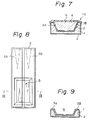
- FIG. 6 is a perspective view showing a preferred embodiment of the miniaturized oxygen electrodes (micro-oxygen electrodes) according to the present invention.
- a micro-oxygen electrode 10 has a rectangular configuration and contains two electrodes 3A and 3B on a silicon oxide (SiO2) insulating layer 2.
- the electrode 10 is a polarographic oxygen electrode and, therefore, the electrodes 3A and 3B are made of gold.
- Reference number 5 is an oxygen gas-permeable membrane covering a sensing portion of the oxygen electrode.
- a silicon (Si) substrate 1 has an insulating layer SiO2 layer 2 formed on an overall surface thereof in addition to a recess-groove formed by anisotropic etching.
- the recess in this instance is in the form of an inverted trapezoid, but any other configuration is acceptable.
- the inverted trapezoid-shaped recess has a pair of Au electrodes 3A and 3B deposited on an inner surface thereof.
- the recess is filled with an electrolyte solution-carrying material (gel) 4, and an upper surface thereof is covered with the oxygen gas-permeable membrane 5.
- the body of the micro-oxygen electrode is further illustrated in Fig. 8 and Fig. 9, which is a cross-sectional view taken along the line IX-IX of Fig. 8.
- the inverted trapezoid-shaped recess described above is indicated by the reference number 6.
- Both of the Au electrodes 3A and 3B extend to the inner surface of the recess 6.
- the length, width and thickness of this electrode body are 15 mm, 4 mm, and 350 ⁇ m, respectively.
- Narrower electrodes such as those having a width of 1 mm, 2 mm or 3 mm can be similarly produced.
- an application of a predetermined voltage (for example, 0.8 volts) between the two Au electrodes 3A and 3B will result in the following reduction reaction at a surface of either of the Au cathodes 3A or 3B.
- a predetermined voltage for example, 0.8 volts
- O2 + 2H2O + 4e ⁇ ⁇ 4OH ⁇ Due to the reduction of oxygen, electrons are discharged from the cathode to the oxygen, and thus an electric current is generated.
- the resulting electric current is proportional to the concentration of oxygen. Accordingly, the concentration of oxygen can be quantitatively determined using the electric current as an index.
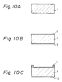
- micro-oxygen electrode of Figs. 6 and 7 can be produced in accordance with a series of fabrication steps shown, for example, in Figs. 10A to 10K. In these figures, the production of only one oxygen electrode is illustrated in sequence, to simplify understanding of the fabrication steps, but it should be noted that, in practice, numerous micro-oxygen electrodes can be concurrently fabricated on a single wafer or silicon substrate.
- a ⁇ 100> oriented p-type silicon wafer having a diameter of 2 inches and a thickness of 350 ⁇ m is prepared.
- the Si wafer 1 is washed successively with an aqueous mixed solution of hydrogen peroxide and ammonia, and conc. nitric acid.
- the Si wafer 1 is subjected to a conventional thermal oxidation in a wet state to form an SiO2 layer 2, which acts as an electrically insulating layer, on an overall surface of the wafer 1.
- the SiO2 layer thus obtained has a thickness of about 1.0 to 1.2 ⁇ m.
- the Si wafer 1 Before anisotropic etching, the Si wafer 1 is covered with a desired pattern 7 of the negative-working photoresist (OMR-83, commercially available from Tokyo Oka Co.).
- OMR-83 commercially available from Tokyo Oka Co.
- the resist pattern 7 is used as a mask in the subsequent step of selective etching of the underlying SiO2 layer 2.
- a lower surface of the Si water 1 not having the resist pattern is coated with the negative-working photoresist, which is identical to that used in the above patterning step.
- the wafer 1 is baked at 120°C for 1 hour, and thus the resist coating 8 is formed.
- a window for anisotropic etching is opened in the SiO2 layer 2 of the Si wafer 1.
- This window formation is performed by dipping the wafer 1 in an aqueous solution of 50% hydrofluoric acid 50% ammonium fluoride (1:6), to etch off the unmasked SiO2 layer, i.e., the SiO2 layer 2 not having the resist pattern 7 (see Fig. 10D).
- the remaining resist is removed in a solution of sulfuric acid and hydrogen peroxide (2:1) at room temperature.
- the window is formed in the SiO2 layer 2, and thus the Si wafer 1 is exposed in an area in which anisotropic etching is carried out in the next step.
- the Si wafer 1 is anisotropically etched in an aqueous solution of 35% potassium hydroxide at 80°C.
- the remaining SiO2 layer 2 on the upper surface of the wafer 1 is used as a mask in this step.
- the wafer 1 is washed with distilled water.
- a recess or groove 6 in the form of inverted trapezoid is formed.
- the SiO2 layer 2 used as the mask in the above step is removed with the same solution as used in step (5). After washing, the wafer 1 is subjected to a conventional wet thermal oxidation at 1000°C, and thus a newly grown SiO2 layer 2 having a thickness of 5000 ⁇ is formed on the upper surface of the wafer 1.
- a pattern of the negative-working photoresist 9 is formed on the SiO2 layer 2 of the Si wafer.
- the resist pattern 9 thus covers SiO2 areas other than those on which electrodes are formed.
- the photoresist used is the same as used in step (3).
- gold 3 as an electrode material is vacuum deposited at a thickness of 1 ⁇ m on an overall surface of the Si wafer 1.
- a chromium layer 500 ⁇ thick (not shown) as deposited to improve the adhesion of the Au layer 3 to the SiO2 layer 2.
- Fig. 10J corresponds to that of Fig. 9.
- An electrolyte solution-carrying gel 4 is filled in the inverted trapezoid-shaped recess of the Si wafer 1.
- agarose is dissolved in an aqueous solution of 0.1M KCl, the solution is added to the recess after heating, using a micro-syringe, and the agarose solution is left to stand.
- the agarose is then cooled and solidified to form a gel, and thus the electrolyte solution-containing gel 4 is produced.
- a silicone resin (SR2410, commercially available from Toray Silicone Co.) is coated on an overall surface of the Si wafer 1.
- the oxygen gas-permeable membrane consisting of silicone resin will strongly adhere to the wafer 1.
- a desired micro-oxygen electrode 10 illustrated in Figs. 6 and 7 is obtained.
- negative-working photoresists such as those used as the pattern forming material in the above-described steps (3) and (8) can be advantageously utilized as the oxygen gas-permeable membrane, since they have a good oxygen gas permeability and exhibit an excellent mechanical and adhesive strength in addition to an ease of coating.
- the negative photoresist: OMR-83 is spin-coated to a thickness of 3 ⁇ m on the Si wafer, followed by exposure to UV rays.
- the photoresist coating capable of functioning as the gas-permeable membrane can be obtained at a relatively low spinning speed, for example, less than 3,000 rpm, but a spinning speed of about 1,500 to 2,000 rpm is preferred because the resulting coating is homogeneous and has a uniform thickness.
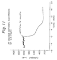
- a response characteristic of the micro-oxygen electrode is determined and plotted as a graph of response time vs. electric current.
- a voltage of 0.6 volts is applied between the Au electrodes.
- a sensing portion of the electrode is dipped into a buffer solution of phosphoric acid having a pH of 7, followed by an addition of sodium sulfite (Na2SO3) to reduce the concentration of oxygen dissolved in the buffer solution.
- Na2SO3 sodium sulfite
- the results of comparison are plotted as a graph of the current of the conventional oxygen electrode vs. that of the micro-oxygen electrode of the present invention, in Fig. 12.
- the results of Fig. 12 indicate that there is a linear relationship between the responses of these two oxygen electrodes, and that the micro-oxygen electrode of the present invention is more sensitive to the change of the concentration of the dissolved oxygen.
- the micro-oxygen electrodes according to the present invention have many advantages derived from their structures and production processes.
- the sizes and characteristics of the resulting micro-oxygen electrodes are uniform because they are produced by a lithographic technique, and although they are very small in size, the fabrication accuracy thereof is high.
- the electrodes can be produced by a mass-production process and, therefore, the costs thereof are notably reduced. This reduction of costs means that the electrodes can be disposed of after use, although they can be repeatedly used if desired.
- an electrolyte solution-containing gel is used in the recess, the electrolyte solution is easily added to the recess and to the recess easily covered with the gas-permeable membrane.
- the electrodes can be used for in vivo measurements.
- the miniaturized oxygen electrodes of the present invention can be used in various fields. For example, they can be advantageously used as a transducer in the production of a miniaturized biosensor which comprises a receptor having biological substances immobilized in an organic medium and a transducer. As previously described, the biosensors can be utilized in chemical analysis, industrial process and environmental conditioning, for example.
- FIG. 13 is a perspective view showing a preferred embodiment of the miniaturized biosensors according to the present invention.
- the illustrated microbiosensor 11 is a glucose microsensor and, as shown in Fig. 14, which is a cross-section along the line XIV-XIV of Fig. 13, has an enzyme-immobilized membrane 12 on a sensitive portion of the micro-oxygen electrode of Fig. 6.
- the microbiosensor of Fig. 13 is produced by forming a receptor on a sensitive portion of the micro-oxygen electrode after the micro-oxygen electrode is produced in accordance with the fabrication steps of Figs. 10A to 10K.
- the receptor of the microsensor can be produced, for example, by dropping 20 ⁇ l of an aqueous solution of 10% bovine serum albumin (BSA), having 5 mg of glucose oxidase (GOD), dissolved therein on a sensitive portion of the micro-oxygen electrode.
- BSA bovine serum albumin
- GOD glucose oxidase
- the sensitive portion of the electrode may be dipped in a mixed solution of 5 mg of GOD, 20 ⁇ l of a 10% BSA solution, and 10 ⁇ l of a 25% GA solution.
- the cross-linking reaction of BSA and GA then proceeds, and finally, as shown in Fig. 14, a GOD-immobilized membrane 12 is firmly adhered to the sensitive portion of the micro-oxygen sensor.
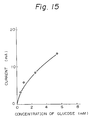
- the glucose microsensor thus produced is then tested to determine the response characteristics thereof.
- a test solution containing glucose is added to the buffer solution.
- Glucose is oxidized with the GOD immobilized on the sensitive portion of the microsensor, and concurrently, oxygen around the micro-oxygen electrode is consumed. Since the oxygen concentration varies, an electric current passed through the electrodes also changes. Based on such a change of electric current, a concentration of glucose can be determined.
- Figure 15 shows a calibration curve of the glucose microsensor, and indicates that the microsensor can respond substantially linearly over a wide range of glucose concentration. This is comparable to conventional glucose sensors.
- amperometric and miniaturized glucose biosensors and other biosensors can be produced with a high fabrication accuracy and by a mass-production process, and can be used for in vivo monitoring, for example, by inserting the sensor into a small space such as catheter. Since the production costs are remarkably reduced, the sensors may be used as disposable products, if desired.
- micro-oxygen electrodes according to the present invention can be produced in the manner described above with reference to Figs. 10A to 10K. Alternatively, they can be produced as follows.
- FIGS 16A to 16F illustrate, in sequence, the production of the micro-oxygen electrode containing an electrolyte solution-carrying polymeric gel. This production process is particularly suited to the mass-production of the electrodes with a low cost.
- the fabrication steps comprise:
- Gold electrodes 3A and 3B are deposited on an SiO2 coating 2 on the Si wafer 1 in the same manner as described with reference to Fig. 10J.
- the preceding steps correspond to those of Figs. 10A to 10I.
- the Si wafer 1 is spin coated with the negative-working photoresist (OMR-83) to wholly cover the wafer 1.
- OMR-83 negative-working photoresist
- the photoresist coating 13 is then prebaked, exposed and developed. As shown in Fig. 16B, the photoresist coating 13 covers the overall surface of the wafer 1 except for the recess portion 6.
- An electrolyte solution-carrying polymeric gel is produced by polymerizing the corresponding photopolymerizable monomers. The following four solutions are prepared for this purpose.
- riboflavin (vitamin B2 , hardening accelerator) is dissolved in an aqueous solution of 0.1M KCl to produce 100 ml.
- the wafer 1 is removed from the aqueous solution 14 of acrylamide.
- the aqueous solution 14 remains only in the recess, because the photoresist 13 is hydrophobic and repels the aqueous solution.
- the wafer 1 is then exposed to radiations 15 generated from a mercury vapor lamp or fluorescent lamp (not shown) to induce polymerization of the acrylaminde in the solution 14, and polymerization proceeds accordingly.
- an electrolyte solution-carrying polymeric gel 16 namely, a porous polyacrylamide having an aqueous solution of KCl impregnated in the pores thereof, is obtained.
- the negative-working photoresist (OMR-83) used in the step of Fig. 16B is again used herein, but as an oxygen gas-permeable membrane, since the resulting coating can exhibit a satisfactory oxygen gas permeability, mechanical strength, and adhesion to the electrolyte-carrying gel.
- the photoresist pattern used as the mask in the previous step is not removed, since it has no adverse affect on this gas-permeable membrane.
- the photoresist (OMR-83) is spun coated to a thickness of about 2 ⁇ m on the wafer 1 and is immediately exposed without prebaking to form a gas-permeable membrane 13. The thinner in the resulting resist or membrane is removed by dipping the wafer in purified water or standing in an atmosphere saturated with wafer vapour for one day and night.
- the micro-oxygen electrodes can be produced in the sequence shown in Figs. 17A to 17F.
- Figures 17A to 17F each correspond to Figs. 16A to 16F previously explained.
- the Au electrodes 3A and 3B are deposited on an SiO2 coating 2 of the Si wafer 1 in the same manner as described with reference to Fig. 10J.
- the preceding steps correspond to those of Figs. 10A to 10I.
- the Si wafer 1 is spin coated with the negative-working photoresist (OMR-83) the wholly cover the wafer 1.
- OMR-83 negative-working photoresist
- the photoresist coating 13 is then prebaked, exposed and developed. As shown in Fig. 17B, the photoresist coating 13 covers the overall surface of the wafer 1 except for the recess portion 6.
- An electrolyte solution-carrying polymeric gel is produced, as in Fig. 16C, by polymerizing the corresponding photopolymerizable monomers.
- the following four solutions are prepared for this purpose.
- riboflavin (vitamin B2, hardening accelerator) is dissolved in an aqueous solution of 0.1M Na2SO4 to produce 100 ml.
- the wafer 1 is removed from the aqueous solution 14 of acrylamide.
- the aqueous solution 14 remains only in the recess, because the photoresist 13 is hydrophobic and repels the aqueous solution.
- the wafer 1 is then immediately covered with a transparent cover glass 17 0.1 mm thick.
- the cover glass 17 used effective prevents evaporation of the electrolyte solution, and in particular, the water content thereof, from the recess of the wafer 1.
- the wafer 1 is exposed to radiations 15 generated from a mercury vapor lamp or fluorescent lamp (not shown) to induce polymerization of the acrylamide in the solution 14, and polymerization proceeds accordingly.
- an electrolyte solution-carrying polymeric gel 16 namely, a porous polyacrylamide having an aqueous solution of Na2SO4 impregnated in pores thereof, is obtained.
- the negative-working photoresist (OMR-83) used in the step of Fig. 17B is again used, but as an oxygen gas-permeable membrane, since the resulting coating exhibits a satisfactory oxygen gas permeability, mechanical strength, and adhesion to the electrolyte-carrying gel.
- the photoresist pattern used as the mask in the previous step is not removed, since it has no adverse affect on this gas-permeable membrane.
- the photoresist (OMR-83) is spin coated to a thickness of about 2 ⁇ m on the wafer 1 and is immediately exposed without prebaking to form a gas-permeable membrane 13. The thinner in the resulting resist or membrane is removed by dipping the wafer in purified water or standing in an atmosphere saturated with water vapor for one day and night.
- electrolyte solution-carrying polymeric gels having a uniform volume, small size and flat surface can be easily produced.
- the formation of a gas-permeable membrane on the surface of the gel also can be easily attained.
- the characteristics of the micro-oxygen electrodes produced are remarkably uniform.
- micro-oxygen electrodes according to the present invention can be produced by using a "sol-gel method" in the formation of the electrolyte solution-containing gel.
- the production process is particularly suited to the mass-production of the micro-oxygen electrodes for use in in vivo measurements, because the materials used in the electrolytecarrying gel have no toxity to the human body.
- Metal alcoxide used as a starting material in the sol-gel method can be represented by the formula: Me(OR) n in which Me is a metal, R is an alkyl group such as methyl and ethyl, and n is an integer.
- Me is a metal
- R is an alkyl group such as methyl and ethyl
- n is an integer.
- this metal alcoxide is tetraethoxysilane Si(OC2H5)4.
- the sol-gel method can be carried out in the manner outlined in the flow sheet of Fig. 19.
- the metal alcoxide is hydrolyzed and then polycondensated, and surprisingly, in this method, the change in volume of the gel before and after gelation is negligible. Thus the gelation can be easily carried out with good results.
- the micro-oxygen electrodes can be produced as follows:
- the Au electrodes 3A and 3B are deposited on an SiO2 layer 2 of the Si wafer 1. This and preceding steps can be carried out in the manner described above in detail with reference to Figs. 16A and 17A, respectively.
- the Si wafer 1 is spin coated with the negative-working photoresist (OMR-83, viscosity 60 cp) to wholly cover the wafer 1.
- OMR-83 negative-working photoresist
- the photoresist coating 13 is then prebaked, exposed and developed. As is shown in Fig. 16B, the photoresist coating 13 covers the overall surface of the wafer 1 except for the recess portion 6.
- a mixed solution of tetraethoxysilane : ethanol : purified wafer (containing 0.15M HCl and 0.1M Na2SO4) in a molar ratio of 1 : 4 : 50 is thoroughly mixed at a room temperature by stirring.
- the resist-coated Si wafer 1 produced in the step of Fig. 18B is then dipped in this aqueous solution 18 containing Na2SO4 as the electrolyte.
- the wafer 1 is removed from the aqueous solution 18.
- the solution 18 remains only in the recess, because the photo-resist 13 is hydrophobic and repels the aqueous solution.
- the wafer 1 is subjected to the sol-gel process by leaving it to stand in an atmosphere saturated with water vapor 19 at 25°C for 24 hours, and Gelation of tetraethoxysilane in the solution 18 proceeds gradually.
- an electrolyte solution-carrying gel 20 namely, a porous gel having an aqueous solution of Na2SO4 impregnated in pores thereof, is obtained.
- the negative-working photoresist (OMR-83) used in the step of Fig. 18B is again used, but as an oxygen gas-permeable membrane and at a different viscosity, since the resulting coating exhibits a satisfactory oxygen gas permeability, mechanical strength, and adhesion to the electrolyte-carrying gel.
- the photo-resist pattern used as the mask in the previous step is not removed, since it has no adverse affect on this gas-permeable membrane.
- the photoresist (OMR-83), viscosity 45 cp) is dip coated to a thickness of about 2 ⁇ m on the wafer 1 and is immediately exposed without prebaking to form a gas-permeable membrane 13. The thinner in the resulting resist or membrane is removed by dipping the wafer in purified water or standing in an atmosphere saturated with water vapour for one day and night.
- the HCl used in the mixed solution in the step (3) is spontaneously removed from the gel during storing.
- the wafer can be immersed in a solution of electrolyte such as 0.1M Na2SO4 for about 24 hours after completion of the gelation.
- electrolyte such as 0.1M Na2SO4
- excess electrolyte adhered on a surface of the wafer can be removed by spraying with N2 gas.
- the gas-permeable membrane is formed as described in step (6).
Claims (35)
- Eine miniaturisierte Sauerstoffelektrode (10), die folgendes umfaßt: ein Substrat (1) mit mindestens einer auf seiner Oberfläche gebildeten Vertiefungsrille (6), zwei Elektroden (3A, 3B), die als eine Kathode und eine Anode wirken und auf einer Isolierschicht (2) an der Oberfläche des Substrates gebildet sind, wobei sich jede der Elektroden in einen Bodenbereich der Vertiefungsrille erstreckt, ein poröses, wäßrige Elektrolytlösung enthaltendes Material (4), das die Vertiefungsrille ausfüllt, und eine sauerstoffgasdurchlässige Membran (5), die die Vertiefungsrille und das darin enthaltene poröse Material bedeckt und abdichtet.
- Die Sauerstoffelektrode (10) nach Anspruch 1, bei der das Substrat (1) ein Halbleitersubstrat ist und die Vertiefungsrille (6) durch fotolithografische und anisotrope Ätzung gebildet wird.
- Die Sauerstoffelektrode (10) nach Anspruch 2, bei der das Halbleitersubstrat (1) aus Silizium hergestellt ist.
- Die Sauerstoffelektrode (10) nach Anspruch 3, bei der die Isolierschicht (2) eine Siliziumoxidschicht ist und durch Oxydieren des Siliziumsubstrats (1) gebildet wird.
- Die Sauerstoffelektrode (10) nach Anspruch 1, bei der die Elektroden (3A, 3B) durch Vakuumabscheidung ausgewählter Metalle gebildet sind.
- Die Sauerstoffelektrode (10) nach Anspruch 1, bei der sowohl die Kathode (3A) als auch die Anode (3B) die gleiche ist und jede eine Gold- oder Platinelektrode darstellt und die Elektrolytlösung in Kontakt mit den Elektroden eine wäßrige Kaliumchloridlösung darstellt.
- Die Sauerstoffelektrode (10) nach Anspruch 1, bei der die Kathode (3A) eine Gold- oder Platinelektrode ist und die Anode (3B) eine Silber-/ Silberchloridelektrode und die Elektrolytlösung in Kontakt mit den Elektroden eine wäßrige Kaliumchloridlösung darstellt.
- Die Sauerstoffelektrode (19) nach Anspruch 1, bei der die Kathode (3B) eine Gold- oder Platinelektrode ist und die Anode (3A) eine Bleielektrode ist und die Elektrolytlösung in Kontakt mit den Elektroden eine wäßrige Kaliumhydroxidlösung darstellt.
- Die Sauerstoffelektrode (10) nach Anspruch 1, bei der die Kathode (3B) eine Gold- oder Platinelektrode ist und die Anode eine Silberelektrode ist und die Elektrolytlösung in Kontakt mit den Elektroden eine wäßrige Kaliumhydroxidlösung darstellt.
- Die Sauerstoffelektrode (10) nach Anspruch 1, bei der das poröse Material ein Agarosegel mit der darin ein geschlossenen Elektrolytlösung ist.
- Die Sauerstoffelektrode (10) nach Anspruch 1, bei der das poröse Material ein polymeres Gel eines fotopolymerisierbaren Monomers mit der darin eingeschlossenen Elektrolytlösung ist.
- Die Sauerstoffelektrode (10) nach Anspruch 11, bei der die fotopolymerisierbaren Monomeren Acrylamid sind.
- Die Sauerstoffelektrode (10) nach Anspruch 1, bei der das poröse Material ein Metallalkoxidgel mit der darin eingeschlossenen Elektrolytlösung ist.
- Die Sauerstoffelektrode (10) nach Anspruch 1, bei der die sauerstoffgasdurchlässige Membran (5) eine Silikonharzbeschichtung ist.
- Die Sauerstoffelektrode (10) nach Anspruch 1, bei der die sauerstoffgasdurchlässige Membran (5) eine Beschichtung aus Fotoresistmaterial ist.
- Ein Verfahren für die Herstellung miniaturisierter Sauerstoffelektroden, das die folgenden Schritte umfaßt:- Bilden zumindest einer Vertiefungsrille (6) auf einem Substrat (1) durch fotolithografische und anisotrope Ätzung,- Bilden einer Isolierschicht (2) an der Oberfläche des mit Vertiefungsrillen versehenen Substrates (1),- Bilden zweier Elektroden (3A, 3B) an der Oberfläche der Isolierschicht dergestalt, daß sich die Elektroden in einen Bodenbereich der Vertiefung erstrecken,- Ausfüllen der Vertiefung mit einem porösen, wäßrigen, die Elektrolytlösung enthaltenden Material (4) und- Bedecken und Abdichten der das poröse Material enthaltenden Vertiefung (6) mit einer sauerstoffgasdurchlässigen Membran (5).
- Das Herstellungsverfahren nach Anspruch 16, bei dem Silizium als ein Substrat verwendet wird und eine Siliziumoxidschicht als die Isolierschicht (2) durch Oxydieren des Siliziumsubstrates (1) gebildet wird.
- Das Herstellungsverfahren nach Anspruch 16, bei dem die Elektroden (3A, 3B) durch Vakuumabscheidung der aus der Gruppe Gold, Platin, Silber, Silber/Silberchlorid und Blei ausgewählten Elektrodenmaterialien gebildet wird.
- Das Herstellungsverfahren nach Anspruch 16, bei dem eine erwärmte Agaroselösung, die die Elektrolytlösung enthält, in die Vertiefung (6) gegossen und stehengelassen wird, um ein Agarosegel mit der darin eingeschlossenen Elektrolytlösung zu bilden.
- Das Herstellungsverfahren nach Anspruch 16, bei dem eine Lösung aus fotopolymerisierbaren Monomeren, die die Elektrolytlösung enthalten, in die Vertiefung (6) gegossen wird und Strahlungen, die zur Auslösung einer Polymerisation der Monomeren in der Lage sind, auf das Substrat (1) gerichtet werden, um ein polymeres Gel mit der darin eingeschlossenen Elektrolytlösung zu bilden.
- Das Herstellungsverfahren nach Anspruch 20, bei dem die fotopolymerisierbaren Monomere Acrylamid sind und die Lösung daraus UV-Strahlen ausgesetzt wird, um deren Polymersisation zu veranlassen.
- Das Herstellungsverfahren nach Anspruch 16, bei dem nach Bildung der Elektroden (3A, 3B) die Oberfläche des Substrats (1) mit Ausnahme des Vertiefungsteils (6) vollständig mit einem hydrophoben Fotoresistmaterial beschichtet wird, das maskierte Substrat in eine wäßrige Lösung aus fotopolymerisierbaren Monomeren, die die Elektrolytlösung enthält, getaucht wird und das die wäßrige Lösung der Monomeren in der Vertiefung enthaltende Substrat Strahlungen ausgesetzt wird, die eine Polymerisation der Monomeren auslösen können, um ein polymeres Gel mit der darin eingeschlossenen Elektrolytlösung zu bilden.
- Das Herstellungsverfahren nach Anspruch 22, bei dem das Substrat (1) den Strahlungen ausgesetzt wird, nachdem die darauf gebildete Vertiefung (6) mit einem verdampfungsverhindernden Mittel, welches den Durchgang der Strahlung erlaubt, bedeckt und abgeschlossen ist.
- Das Herstellungsverfahren nach Anspruch 22 oder 23, bei dem die fotopolymerisierbaren Monomeren Acrylamid sind und die Lösung davon UV-Strahlen ausgesetzt wird, um ihre Polymerisation zu veranlassen.
- Das Herstellungsverfahren nach Anspruch 16, bei dem eine die Elektrolytlösung enthaltende Metallalkoxidlösung in die Vertiefung gegossen und einem Sol-Gel-Prozeß unterzogen wird, um ein Metallalkoxidgel mit der darin eingeschlossenen Elektrolytlösung zu bilden.
- Das Herstellungsverfahren nach Anspruch 25, bei dem das Metallalkoxid Tetraethoxysilan ist.
- Das Herstellungsverfahren nach Anspruch 16, bei dem nach Bildung der Elektroden die Oberfläche des Substrats (1), mit Ausnahme des Vertiefungsteils, vollständig mit einem hydrophoben Fotoresistmaterial beschichtet wird, das maskierte Substrat in eine die Elektrolytlösung enthaltende wäßrige Lösung von Metallalkoxid getaucht wird und das Substrat (1), das die wäßrige Lösung des Metallalkoxids in der Vertiefung enthält, einem Sol-Gel-Prozeß unterzogen wird, um ein Gel des Metallalkoxids mit der darin eingeschlossenen Elektrolytlösung zu bilden.
- Das Herstellungsverfahren nach Anspruch 27, bei dem das Metallalkoxid Tetraethoxysilan ist.
- Das Herstellungsverfahren nach Anspruch 16, bei dem die das poröse Material enthaltende Vertiefung mit einem Silikonharz beschichtet wird, um die sauerstoffgasdurchlässige Membran zu bilden.
- Das Herstellungsverfahren nach Anspruch 16, bei dem die das poröse Material enthaltende Vertiefung (6) mit einem Fotoresistmaterial beschichtet wird, um die sauerstoffgasdurchlässige Membran (5) zu bilden.
- Ein miniaturisierten Biofühler (10), der im wesentlichen besteht aus einer Sauerstoffelektrode, umfassend ein Substrat (1) mit zumindest einer Vertiefungsrille (6), gebildet auf einer Oberfläche davon, zwei Elektroden (3A, 3B), die als eine Kathode und eine Anode wirken und auf einer Isolierschicht (2) an der Oberfläche des Substrats gebildet werden, von denen sich jede der Elektroden in einen Bodenbereich der Vertiefungsrille erstreckt, ein poröses, die wäßrige Elektrolytlösung enthaltendes Material (4), das die Vertiefungsrille ausfüllt, eine sauerstoffgasdurchlässige Membran, die die Vertiefungsrille und das darin enthaltene poröse Material bedeckt und abdichtet, und eine immobilisierte biologische Substanz, die die Oxydation der biochemischen organischen Verbindungen katalysieren kann und an einer sensitiven Stelle der Sauerstoffelektrode positioniert ist.
- Der Biofühler (10) nach Anspruch 31, bei dem die biologische Substanz ein Enzym oder ein Gemisch aus zwei oder mehr Enzymen ist.
- Der Biofühler (10) nach Anspruch 31, bei dem die biologische Substanz ein Mikroorganismus ist.
- Der Biofühler (10) nach Anspruch 31, bei dem die biologische Substanz ein Gemisch aus zwei oder mehr Enzymen und Mikroorganismen ist.
- Der Biofühler (10) nach Anspruch 31, der ein Glucosefühler ist.
Applications Claiming Priority (10)
| Application Number | Priority Date | Filing Date | Title |
|---|---|---|---|
| JP62071739A JPH061254B2 (ja) | 1987-03-27 | 1987-03-27 | 酸素電極 |
| JP71739/87 | 1987-03-27 | ||
| JP62071738A JPS63238549A (ja) | 1987-03-27 | 1987-03-27 | マイクロバイオセンサ |
| JP71738/87 | 1987-03-27 | ||
| JP62148221A JPH0812171B2 (ja) | 1987-06-15 | 1987-06-15 | 小形酸素電極の製造方法 |
| JP148221/87 | 1987-06-15 | ||
| JP63047363A JPH01223336A (ja) | 1988-03-02 | 1988-03-02 | 小型酸素電極及びその製法 |
| JP47363/88 | 1988-03-02 | ||
| JP48708/88 | 1988-03-03 | ||
| JP63048708A JPH01223337A (ja) | 1988-03-03 | 1988-03-03 | 小型酸素電極の製法 |
Publications (3)
| Publication Number | Publication Date |
|---|---|
| EP0284518A2 EP0284518A2 (de) | 1988-09-28 |
| EP0284518A3 EP0284518A3 (en) | 1989-11-29 |
| EP0284518B1 true EP0284518B1 (de) | 1992-10-07 |
Family
ID=27522619
Family Applications (1)
| Application Number | Title | Priority Date | Filing Date |
|---|---|---|---|
| EP88400742A Expired - Lifetime EP0284518B1 (de) | 1987-03-27 | 1988-03-25 | Miniaturisierter Biofühler mit miniaturisierter Sauerstoffelektrode sowie sein Herstellungsverfahren |
Country Status (3)
| Country | Link |
|---|---|
| US (1) | US4975175A (de) |
| EP (1) | EP0284518B1 (de) |
| DE (1) | DE3875149T2 (de) |
Cited By (34)
| Publication number | Priority date | Publication date | Assignee | Title |
|---|---|---|---|---|
| US7654956B2 (en) | 2004-07-13 | 2010-02-02 | Dexcom, Inc. | Transcutaneous analyte sensor |
| US7711402B2 (en) | 1997-03-04 | 2010-05-04 | Dexcom, Inc. | Device and method for determining analyte levels |
| US7761130B2 (en) | 2003-07-25 | 2010-07-20 | Dexcom, Inc. | Dual electrode system for a continuous analyte sensor |
| US7771352B2 (en) | 1997-03-04 | 2010-08-10 | Dexcom, Inc. | Low oxygen in vivo analyte sensor |
| US7783333B2 (en) | 2004-07-13 | 2010-08-24 | Dexcom, Inc. | Transcutaneous medical device with variable stiffness |
| US7831287B2 (en) | 2006-10-04 | 2010-11-09 | Dexcom, Inc. | Dual electrode system for a continuous analyte sensor |
| US7857760B2 (en) | 2004-07-13 | 2010-12-28 | Dexcom, Inc. | Analyte sensor |
| US7905833B2 (en) | 2004-07-13 | 2011-03-15 | Dexcom, Inc. | Transcutaneous analyte sensor |
| US8133178B2 (en) | 2006-02-22 | 2012-03-13 | Dexcom, Inc. | Analyte sensor |
| US8160671B2 (en) | 2003-12-05 | 2012-04-17 | Dexcom, Inc. | Calibration techniques for a continuous analyte sensor |
| US8162829B2 (en) | 1998-04-30 | 2012-04-24 | Abbott Diabetes Care Inc. | Analyte monitoring device and methods of use |
| USRE43399E1 (en) | 2003-07-25 | 2012-05-22 | Dexcom, Inc. | Electrode systems for electrochemical sensors |
| US8275437B2 (en) | 2003-08-01 | 2012-09-25 | Dexcom, Inc. | Transcutaneous analyte sensor |
| US8280475B2 (en) | 2004-07-13 | 2012-10-02 | Dexcom, Inc. | Transcutaneous analyte sensor |
| US8287454B2 (en) | 1998-04-30 | 2012-10-16 | Abbott Diabetes Care Inc. | Analyte monitoring device and methods of use |
| US8287453B2 (en) | 2003-12-05 | 2012-10-16 | Dexcom, Inc. | Analyte sensor |
| US8346337B2 (en) | 1998-04-30 | 2013-01-01 | Abbott Diabetes Care Inc. | Analyte monitoring device and methods of use |
| US8396528B2 (en) | 2008-03-25 | 2013-03-12 | Dexcom, Inc. | Analyte sensor |
| US8394021B2 (en) | 2003-08-01 | 2013-03-12 | Dexcom, Inc. | System and methods for processing analyte sensor data |
| US8417312B2 (en) | 2007-10-25 | 2013-04-09 | Dexcom, Inc. | Systems and methods for processing sensor data |
| US8423114B2 (en) | 2006-10-04 | 2013-04-16 | Dexcom, Inc. | Dual electrode system for a continuous analyte sensor |
| US8465425B2 (en) | 1998-04-30 | 2013-06-18 | Abbott Diabetes Care Inc. | Analyte monitoring device and methods of use |
| US8509871B2 (en) | 2001-07-27 | 2013-08-13 | Dexcom, Inc. | Sensor head for use with implantable devices |
| US8565848B2 (en) | 2004-07-13 | 2013-10-22 | Dexcom, Inc. | Transcutaneous analyte sensor |
| US8612159B2 (en) | 1998-04-30 | 2013-12-17 | Abbott Diabetes Care Inc. | Analyte monitoring device and methods of use |
| US8622905B2 (en) | 2003-08-01 | 2014-01-07 | Dexcom, Inc. | System and methods for processing analyte sensor data |
| US8652043B2 (en) | 2001-01-02 | 2014-02-18 | Abbott Diabetes Care Inc. | Analyte monitoring device and methods of use |
| US8688188B2 (en) | 1998-04-30 | 2014-04-01 | Abbott Diabetes Care Inc. | Analyte monitoring device and methods of use |
| US8974386B2 (en) | 1998-04-30 | 2015-03-10 | Abbott Diabetes Care Inc. | Analyte monitoring device and methods of use |
| US9066695B2 (en) | 1998-04-30 | 2015-06-30 | Abbott Diabetes Care Inc. | Analyte monitoring device and methods of use |
| US9155496B2 (en) | 1997-03-04 | 2015-10-13 | Dexcom, Inc. | Low oxygen in vivo analyte sensor |
| US9247900B2 (en) | 2004-07-13 | 2016-02-02 | Dexcom, Inc. | Analyte sensor |
| US9451908B2 (en) | 2006-10-04 | 2016-09-27 | Dexcom, Inc. | Analyte sensor |
| US9451910B2 (en) | 2007-09-13 | 2016-09-27 | Dexcom, Inc. | Transcutaneous analyte sensor |
Families Citing this family (69)
| Publication number | Priority date | Publication date | Assignee | Title |
|---|---|---|---|---|
| JP2633281B2 (ja) * | 1988-02-10 | 1997-07-23 | 日本電気株式会社 | 電気化学センサ及びその製造方法 |
| EP0396788A1 (de) * | 1989-05-08 | 1990-11-14 | Dräger Nederland B.V. | Verfahren und Sensor zur Messung des Glucosegehalts von Glucose enthaltenden Flüssigkeiten |
| JPH03183943A (ja) * | 1989-12-14 | 1991-08-09 | Hitachi Ltd | 酸素センサ |
| US5161532A (en) * | 1990-04-19 | 1992-11-10 | Teknekron Sensor Development Corporation | Integral interstitial fluid sensor |
| US5431806A (en) * | 1990-09-17 | 1995-07-11 | Fujitsu Limited | Oxygen electrode and temperature sensor |
| KR960012335B1 (ko) * | 1990-09-17 | 1996-09-18 | 후지쓰 가부시끼가이샤 | 산소전극 |
| US5358619A (en) * | 1990-09-17 | 1994-10-25 | Fujitsu Limited | Oxygen electrode |
| US5152882A (en) * | 1990-09-28 | 1992-10-06 | Rosemount Inc. | Integral hydrolysis layer junction |
| DE69128128T2 (de) * | 1990-12-06 | 1998-03-05 | Fujitsu Ltd | Kleine Glaselektrode und Verfahren für deren Herstellung |
| US5837113A (en) * | 1990-12-06 | 1998-11-17 | Fujitsu Limited | Small glass electrode |
| JP3025027B2 (ja) * | 1991-01-21 | 2000-03-27 | 株式会社日立製作所 | 酸素センサ |
| US5492611A (en) * | 1991-03-20 | 1996-02-20 | Fujitsu Limited | Miniaturized oxygen electrode |
| US5573649A (en) * | 1991-03-20 | 1996-11-12 | Fujitsu Limited | Miniaturized oxygen electrode and process of producing same |
| US5281323A (en) * | 1991-03-20 | 1994-01-25 | Fujitsu Limited | Electrolyte composition for screen printing and miniaturized oxygen electrode and production process thereof |
| US5326450A (en) * | 1991-03-20 | 1994-07-05 | Fujitsu Limited | Miniaturized oxygen electrode |
| JP2512843B2 (ja) * | 1991-09-24 | 1996-07-03 | 株式会社日立製作所 | 炭酸ガスセンサ |
| US5415164A (en) * | 1991-11-04 | 1995-05-16 | Biofield Corp. | Apparatus and method for screening and diagnosing trauma or disease in body tissues |
| US5284139A (en) * | 1991-12-30 | 1994-02-08 | Abbot Laboratories | Hemometrix temperature compensation |
| JPH0634596A (ja) * | 1992-07-20 | 1994-02-08 | Fujitsu Ltd | 酸素電極、バイオセンサ、及び、その製造方法 |
| GB9218376D0 (en) * | 1992-08-28 | 1992-10-14 | Cranfield Inst Of Tech | Media for biocatalytic electrochemical reactions in the gaseous phase |
| US5387329A (en) * | 1993-04-09 | 1995-02-07 | Ciba Corning Diagnostics Corp. | Extended use planar sensors |
| US5690808A (en) * | 1996-01-25 | 1997-11-25 | Teledyne Industries, Inc. | Electrochemical gas sensors and methods for sensing electrochemical active gases in gas mixtures |
| EP0789236B1 (de) * | 1996-02-07 | 2002-04-24 | Motorola, Inc. | Sensor zur Erfassung von Umgebungsbedingungen |
| US7244622B2 (en) * | 1996-04-03 | 2007-07-17 | Applera Corporation | Device and method for multiple analyte detection |
| US5830136A (en) * | 1996-10-31 | 1998-11-03 | Nellcor Puritan Bennett Incorporated | Gel pad optical sensor |
| US5932799A (en) * | 1997-07-21 | 1999-08-03 | Ysi Incorporated | Microfluidic analyzer module |
| US6073482A (en) * | 1997-07-21 | 2000-06-13 | Ysi Incorporated | Fluid flow module |
| US6293012B1 (en) | 1997-07-21 | 2001-09-25 | Ysi Incorporated | Method of making a fluid flow module |
| US6259937B1 (en) | 1997-09-12 | 2001-07-10 | Alfred E. Mann Foundation | Implantable substrate sensor |
| US6287831B1 (en) * | 1997-11-14 | 2001-09-11 | California Institute Of Technology | Cell lysis device |
| JP3874321B2 (ja) * | 1998-06-11 | 2007-01-31 | 松下電器産業株式会社 | バイオセンサ |
| US6387724B1 (en) | 1999-02-26 | 2002-05-14 | Dynamics Research Corporation | Method of fabricating silicon-on-insulator sensor having silicon oxide sensing surface |
| DE19924856A1 (de) * | 1999-05-31 | 2000-12-21 | Intermedical S A H | Elektrochemischer Sensor |
| US6645359B1 (en) | 2000-10-06 | 2003-11-11 | Roche Diagnostics Corporation | Biosensor |
| US6434420B1 (en) | 2000-01-31 | 2002-08-13 | Integrated Biosensing Technologies | Biopotential electrode sensory component |
| US6438413B1 (en) | 2000-01-31 | 2002-08-20 | Integrated Biosensing Technologies | Biopotential sensor electrode system |
| US6434421B1 (en) | 2000-01-31 | 2002-08-13 | Integrated Biosensing Technologies | Biopotential sensor electrode |
| US6405066B1 (en) * | 2000-03-17 | 2002-06-11 | The Regents Of The University Of California | Implantable analyte sensor |
| WO2001069222A2 (en) * | 2000-03-17 | 2001-09-20 | F. Hoffmann-La Roche Ag | Implantable analyte sensor |
| JP3759039B2 (ja) * | 2000-05-11 | 2006-03-22 | 松下エコシステムズ株式会社 | 化学センサデバイス |
| DE10023353A1 (de) * | 2000-05-12 | 2001-11-29 | Osram Opto Semiconductors Gmbh | Optoelektronisches Bauelement und Verfahren zur Herstellung |
| US6764652B2 (en) * | 2001-01-24 | 2004-07-20 | The Regents Of The University Of Michigan | Micromachined device for receiving and retaining at least one liquid droplet, method of making the device and method of using the device |
| CA2347388A1 (en) * | 2001-05-10 | 2002-11-10 | Envitec-Wismar Gmbh | Electrochemical gas sensor |
| DE10240921B4 (de) * | 2002-09-02 | 2007-12-13 | Qimonda Ag | Verfahren und Anordnung zum selektiven Metallisieren von 3-D-Strukturen |
| US20080119703A1 (en) | 2006-10-04 | 2008-05-22 | Mark Brister | Analyte sensor |
| US20190357827A1 (en) | 2003-08-01 | 2019-11-28 | Dexcom, Inc. | Analyte sensor |
| US7920906B2 (en) | 2005-03-10 | 2011-04-05 | Dexcom, Inc. | System and methods for processing analyte sensor data for sensor calibration |
| US11633133B2 (en) | 2003-12-05 | 2023-04-25 | Dexcom, Inc. | Dual electrode system for a continuous analyte sensor |
| US7666285B1 (en) | 2004-02-06 | 2010-02-23 | University Of Central Florida Research Foundation, Inc. | Portable water quality monitoring system |
| DE102004019357A1 (de) * | 2004-04-21 | 2005-11-17 | Infineon Technologies Ag | Verfahren zur Funktionalisierung von Biosensor-Chips |
| US20070045902A1 (en) | 2004-07-13 | 2007-03-01 | Brauker James H | Analyte sensor |
| US8728289B2 (en) * | 2005-12-15 | 2014-05-20 | Medtronic, Inc. | Monolithic electrodes and pH transducers |
| US9757061B2 (en) | 2006-01-17 | 2017-09-12 | Dexcom, Inc. | Low oxygen in vivo analyte sensor |
| JP5405916B2 (ja) * | 2008-06-24 | 2014-02-05 | パナソニック株式会社 | バイオセンサ、その製造方法、及びそれを備える検出システム |
| WO2012054043A1 (en) | 2010-10-21 | 2012-04-26 | Hewlett-Packard Development Company, L.P. | Nano-structure and method of making the same |
| US9751755B2 (en) * | 2010-10-21 | 2017-09-05 | Hewlett-Packard Development Company, L.P. | Method of forming a micro-structure |
| US20170267520A1 (en) | 2010-10-21 | 2017-09-21 | Hewlett-Packard Development Company, L.P. | Method of forming a micro-structure |
| JP5661424B2 (ja) | 2010-10-29 | 2015-01-28 | アークレイ株式会社 | 電気化学センサ |
| DK3575796T3 (da) | 2011-04-15 | 2021-01-18 | Dexcom Inc | Avanceret analytsensorkalibrering og fejldetektion |
| US20140127791A1 (en) * | 2011-07-28 | 2014-05-08 | Siemens Aktiengesellschaft | Diagnostic device |
| DE102011083675A1 (de) * | 2011-09-29 | 2013-04-04 | Endress + Hauser Conducta Gesellschaft für Mess- und Regeltechnik mbH + Co. KG | Sensor zur Bestimmung und/oder Überwachung von zumindest einer gelösten Substanz in einem Medium |
| CN104034770A (zh) * | 2014-07-01 | 2014-09-10 | 安徽马钢自动化信息技术有限公司 | 一种微氧分析仪的热备探头 |
| US20170102355A1 (en) * | 2015-10-09 | 2017-04-13 | Patrick M. McGuinness | Electrochemical sensor, and a method of forming an electrochemical sensor |
| US10620151B2 (en) | 2016-08-30 | 2020-04-14 | Analog Devices Global | Electrochemical sensor, and a method of forming an electrochemical sensor |
| US11268927B2 (en) | 2016-08-30 | 2022-03-08 | Analog Devices International Unlimited Company | Electrochemical sensor, and a method of forming an electrochemical sensor |
| US11022579B2 (en) | 2018-02-05 | 2021-06-01 | Analog Devices International Unlimited Company | Retaining cap |
| CN113351265B (zh) * | 2021-05-26 | 2022-10-25 | 西安交通大学 | 一种基于微导线磁场驱动微流体磁混合的系统的加工方法 |
| EP4170336A3 (de) * | 2022-10-06 | 2023-06-14 | Mettler-Toledo GmbH | Sensor und vorrichtung für einen sensor mit gelelektrolyt |
| EP4350338A1 (de) * | 2022-10-06 | 2024-04-10 | Mettler-Toledo GmbH | Sensor und vorrichtung für einen sensor mit gelelektrolyt |
Family Cites Families (8)
| Publication number | Priority date | Publication date | Assignee | Title |
|---|---|---|---|---|
| US4062750A (en) * | 1974-12-18 | 1977-12-13 | James Francis Butler | Thin film electrochemical electrode and cell |
| FR2425641A1 (fr) * | 1978-05-12 | 1979-12-07 | Thomson Csf | Cellule polarographique et son procede de fabrication |
| FR2426904A1 (fr) * | 1978-05-23 | 1979-12-21 | Thomson Csf | Cellule polarographique et son procede de fabrication |
| US4534356A (en) * | 1982-07-30 | 1985-08-13 | Diamond Shamrock Chemicals Company | Solid state transcutaneous blood gas sensors |
| FR2541462A1 (fr) * | 1983-02-17 | 1984-08-24 | Texaim | Electrode de reference electrochimique miniature |
| US4505799A (en) * | 1983-12-08 | 1985-03-19 | General Signal Corporation | ISFET sensor and method of manufacture |
| JPS61120053A (ja) * | 1984-11-16 | 1986-06-07 | Shimadzu Corp | バイオセンサ |
| US4874500A (en) * | 1987-07-15 | 1989-10-17 | Sri International | Microelectrochemical sensor and sensor array |
-
1988
- 1988-03-25 EP EP88400742A patent/EP0284518B1/de not_active Expired - Lifetime
- 1988-03-25 DE DE8888400742T patent/DE3875149T2/de not_active Expired - Fee Related
-
1989
- 1989-06-15 US US07/366,365 patent/US4975175A/en not_active Expired - Lifetime
Non-Patent Citations (1)
| Title |
|---|
| PATENT ABSTRACTS OF JAPAN vol.10, no. 305 (P-507)(2361), 17 october 1986; & JP-A-61120053 (SHIMADZU CORP.) 07.06.1986 * |
Cited By (127)
| Publication number | Priority date | Publication date | Assignee | Title |
|---|---|---|---|---|
| US9155496B2 (en) | 1997-03-04 | 2015-10-13 | Dexcom, Inc. | Low oxygen in vivo analyte sensor |
| US7771352B2 (en) | 1997-03-04 | 2010-08-10 | Dexcom, Inc. | Low oxygen in vivo analyte sensor |
| US7901354B2 (en) | 1997-03-04 | 2011-03-08 | Dexcom, Inc. | Low oxygen in vivo analyte sensor |
| US7711402B2 (en) | 1997-03-04 | 2010-05-04 | Dexcom, Inc. | Device and method for determining analyte levels |
| US8366614B2 (en) | 1998-04-30 | 2013-02-05 | Abbott Diabetes Care Inc. | Analyte monitoring device and methods of use |
| US8738109B2 (en) | 1998-04-30 | 2014-05-27 | Abbott Diabetes Care Inc. | Analyte monitoring device and methods of use |
| US8734348B2 (en) | 1998-04-30 | 2014-05-27 | Abbott Diabetes Care Inc. | Analyte monitoring device and methods of use |
| US9326714B2 (en) | 1998-04-30 | 2016-05-03 | Abbott Diabetes Care Inc. | Analyte monitoring device and methods of use |
| US8688188B2 (en) | 1998-04-30 | 2014-04-01 | Abbott Diabetes Care Inc. | Analyte monitoring device and methods of use |
| US8672844B2 (en) | 1998-04-30 | 2014-03-18 | Abbott Diabetes Care Inc. | Analyte monitoring device and methods of use |
| US9072477B2 (en) | 1998-04-30 | 2015-07-07 | Abbott Diabetes Care Inc. | Analyte monitoring device and methods of use |
| US9066695B2 (en) | 1998-04-30 | 2015-06-30 | Abbott Diabetes Care Inc. | Analyte monitoring device and methods of use |
| US9066697B2 (en) | 1998-04-30 | 2015-06-30 | Abbott Diabetes Care Inc. | Analyte monitoring device and methods of use |
| US9066694B2 (en) | 1998-04-30 | 2015-06-30 | Abbott Diabetes Care Inc. | Analyte monitoring device and methods of use |
| US8670815B2 (en) | 1998-04-30 | 2014-03-11 | Abbott Diabetes Care Inc. | Analyte monitoring device and methods of use |
| US8162829B2 (en) | 1998-04-30 | 2012-04-24 | Abbott Diabetes Care Inc. | Analyte monitoring device and methods of use |
| US8175673B2 (en) | 1998-04-30 | 2012-05-08 | Abbott Diabetes Care Inc. | Analyte monitoring device and methods of use |
| US8177716B2 (en) | 1998-04-30 | 2012-05-15 | Abbott Diabetes Care Inc. | Analyte monitoring device and methods of use |
| US8666469B2 (en) | 1998-04-30 | 2014-03-04 | Abbott Diabetes Care Inc. | Analyte monitoring device and methods of use |
| US8224413B2 (en) | 1998-04-30 | 2012-07-17 | Abbott Diabetes Care Inc. | Analyte monitoring device and methods of use |
| US8226557B2 (en) | 1998-04-30 | 2012-07-24 | Abbott Diabetes Care Inc. | Analyte monitoring device and methods of use |
| US8226558B2 (en) | 1998-04-30 | 2012-07-24 | Abbott Diabetes Care Inc. | Analyte monitoring device and methods of use |
| US8226555B2 (en) | 1998-04-30 | 2012-07-24 | Abbott Diabetes Care Inc. | Analyte monitoring device and methods of use |
| US9042953B2 (en) | 1998-04-30 | 2015-05-26 | Abbott Diabetes Care Inc. | Analyte monitoring device and methods of use |
| US8231532B2 (en) | 1998-04-30 | 2012-07-31 | Abbott Diabetes Care Inc. | Analyte monitoring device and methods of use |
| US8235896B2 (en) | 1998-04-30 | 2012-08-07 | Abbott Diabetes Care Inc. | Analyte monitoring device and methods of use |
| US8734346B2 (en) | 1998-04-30 | 2014-05-27 | Abbott Diabetes Care Inc. | Analyte monitoring device and methods of use |
| US8255031B2 (en) | 1998-04-30 | 2012-08-28 | Abbott Diabetes Care Inc. | Analyte monitoring device and methods of use |
| US8260392B2 (en) | 1998-04-30 | 2012-09-04 | Abbott Diabetes Care Inc. | Analyte monitoring device and methods of use |
| US8265726B2 (en) | 1998-04-30 | 2012-09-11 | Abbott Diabetes Care Inc. | Analyte monitoring device and methods of use |
| US8275439B2 (en) | 1998-04-30 | 2012-09-25 | Abbott Diabetes Care Inc. | Analyte monitoring device and methods of use |
| US8273022B2 (en) | 1998-04-30 | 2012-09-25 | Abbott Diabetes Care Inc. | Analyte monitoring device and methods of use |
| US8660627B2 (en) | 1998-04-30 | 2014-02-25 | Abbott Diabetes Care Inc. | Analyte monitoring device and methods of use |
| US9011331B2 (en) | 1998-04-30 | 2015-04-21 | Abbott Diabetes Care Inc. | Analyte monitoring device and methods of use |
| US8287454B2 (en) | 1998-04-30 | 2012-10-16 | Abbott Diabetes Care Inc. | Analyte monitoring device and methods of use |
| US8372005B2 (en) | 1998-04-30 | 2013-02-12 | Abbott Diabetes Care Inc. | Analyte monitoring device and methods of use |
| US8306598B2 (en) | 1998-04-30 | 2012-11-06 | Abbott Diabetes Care Inc. | Analyte monitoring device and methods of use |
| US9014773B2 (en) | 1998-04-30 | 2015-04-21 | Abbott Diabetes Care Inc. | Analyte monitoring device and methods of use |
| US8346337B2 (en) | 1998-04-30 | 2013-01-01 | Abbott Diabetes Care Inc. | Analyte monitoring device and methods of use |
| US8346336B2 (en) | 1998-04-30 | 2013-01-01 | Abbott Diabetes Care Inc. | Analyte monitoring device and methods of use |
| US8353829B2 (en) | 1998-04-30 | 2013-01-15 | Abbott Diabetes Care Inc. | Analyte monitoring device and methods of use |
| US8357091B2 (en) | 1998-04-30 | 2013-01-22 | Abbott Diabetes Care Inc. | Analyte monitoring device and methods of use |
| US8641619B2 (en) | 1998-04-30 | 2014-02-04 | Abbott Diabetes Care Inc. | Analyte monitoring device and methods of use |
| US8649841B2 (en) | 1998-04-30 | 2014-02-11 | Abbott Diabetes Care Inc. | Analyte monitoring device and methods of use |
| US8622906B2 (en) | 1998-04-30 | 2014-01-07 | Abbott Diabetes Care Inc. | Analyte monitoring device and methods of use |
| US8391945B2 (en) | 1998-04-30 | 2013-03-05 | Abbott Diabetes Care Inc. | Analyte monitoring device and methods of use |
| US8617071B2 (en) | 1998-04-30 | 2013-12-31 | Abbott Diabetes Care Inc. | Analyte monitoring device and methods of use |
| US8744545B2 (en) | 1998-04-30 | 2014-06-03 | Abbott Diabetes Care Inc. | Analyte monitoring device and methods of use |
| US8380273B2 (en) | 1998-04-30 | 2013-02-19 | Abbott Diabetes Care Inc. | Analyte monitoring device and methods of use |
| US8409131B2 (en) | 1998-04-30 | 2013-04-02 | Abbott Diabetes Care Inc. | Analyte monitoring device and methods of use |
| US8974386B2 (en) | 1998-04-30 | 2015-03-10 | Abbott Diabetes Care Inc. | Analyte monitoring device and methods of use |
| US8612159B2 (en) | 1998-04-30 | 2013-12-17 | Abbott Diabetes Care Inc. | Analyte monitoring device and methods of use |
| US8597189B2 (en) | 1998-04-30 | 2013-12-03 | Abbott Diabetes Care Inc. | Analyte monitoring device and methods of use |
| US8774887B2 (en) | 1998-04-30 | 2014-07-08 | Abbott Diabetes Care Inc. | Analyte monitoring device and methods of use |
| US8880137B2 (en) | 1998-04-30 | 2014-11-04 | Abbott Diabetes Care Inc. | Analyte monitoring device and methods of use |
| US8465425B2 (en) | 1998-04-30 | 2013-06-18 | Abbott Diabetes Care Inc. | Analyte monitoring device and methods of use |
| US8473021B2 (en) | 1998-04-30 | 2013-06-25 | Abbott Diabetes Care Inc. | Analyte monitoring device and methods of use |
| US8840553B2 (en) | 1998-04-30 | 2014-09-23 | Abbott Diabetes Care Inc. | Analyte monitoring device and methods of use |
| US8480580B2 (en) | 1998-04-30 | 2013-07-09 | Abbott Diabetes Care Inc. | Analyte monitoring device and methods of use |
| US9011332B2 (en) | 2001-01-02 | 2015-04-21 | Abbott Diabetes Care Inc. | Analyte monitoring device and methods of use |
| US8652043B2 (en) | 2001-01-02 | 2014-02-18 | Abbott Diabetes Care Inc. | Analyte monitoring device and methods of use |
| US9498159B2 (en) | 2001-01-02 | 2016-11-22 | Abbott Diabetes Care Inc. | Analyte monitoring device and methods of use |
| US8668645B2 (en) | 2001-01-02 | 2014-03-11 | Abbott Diabetes Care Inc. | Analyte monitoring device and methods of use |
| US9328371B2 (en) | 2001-07-27 | 2016-05-03 | Dexcom, Inc. | Sensor head for use with implantable devices |
| US8509871B2 (en) | 2001-07-27 | 2013-08-13 | Dexcom, Inc. | Sensor head for use with implantable devices |
| US7896809B2 (en) | 2003-07-25 | 2011-03-01 | Dexcom, Inc. | Dual electrode system for a continuous analyte sensor |
| USRE43399E1 (en) | 2003-07-25 | 2012-05-22 | Dexcom, Inc. | Electrode systems for electrochemical sensors |
| US7761130B2 (en) | 2003-07-25 | 2010-07-20 | Dexcom, Inc. | Dual electrode system for a continuous analyte sensor |
| US8676287B2 (en) | 2003-08-01 | 2014-03-18 | Dexcom, Inc. | System and methods for processing analyte sensor data |
| US8986209B2 (en) | 2003-08-01 | 2015-03-24 | Dexcom, Inc. | Transcutaneous analyte sensor |
| US8622905B2 (en) | 2003-08-01 | 2014-01-07 | Dexcom, Inc. | System and methods for processing analyte sensor data |
| US8700117B2 (en) | 2003-08-01 | 2014-04-15 | Dexcom, Inc. | System and methods for processing analyte sensor data |
| US8788006B2 (en) | 2003-08-01 | 2014-07-22 | Dexcom, Inc. | System and methods for processing analyte sensor data |
| US8394021B2 (en) | 2003-08-01 | 2013-03-12 | Dexcom, Inc. | System and methods for processing analyte sensor data |
| US8275437B2 (en) | 2003-08-01 | 2012-09-25 | Dexcom, Inc. | Transcutaneous analyte sensor |
| US8483793B2 (en) | 2003-12-05 | 2013-07-09 | Dexcom, Inc. | Dual electrode system for a continuous analyte sensor |
| US8249684B2 (en) | 2003-12-05 | 2012-08-21 | Dexcom, Inc. | Calibration techniques for a continuous analyte sensor |
| US8160671B2 (en) | 2003-12-05 | 2012-04-17 | Dexcom, Inc. | Calibration techniques for a continuous analyte sensor |
| US9579053B2 (en) | 2003-12-05 | 2017-02-28 | Dexcom, Inc. | Dual electrode system for a continuous analyte sensor |
| US8929968B2 (en) | 2003-12-05 | 2015-01-06 | Dexcom, Inc. | Dual electrode system for a continuous analyte sensor |
| US8428678B2 (en) | 2003-12-05 | 2013-04-23 | Dexcom, Inc. | Calibration techniques for a continuous analyte sensor |
| US8911369B2 (en) | 2003-12-05 | 2014-12-16 | Dexcom, Inc. | Dual electrode system for a continuous analyte sensor |
| US8287453B2 (en) | 2003-12-05 | 2012-10-16 | Dexcom, Inc. | Analyte sensor |
| USRE44695E1 (en) | 2003-12-05 | 2014-01-07 | Dexcom, Inc. | Dual electrode system for a continuous analyte sensor |
| US8515519B2 (en) | 2004-07-13 | 2013-08-20 | Dexcom, Inc. | Transcutaneous analyte sensor |
| US8313434B2 (en) | 2004-07-13 | 2012-11-20 | Dexcom, Inc. | Analyte sensor inserter system |
| US8690775B2 (en) | 2004-07-13 | 2014-04-08 | Dexcom, Inc. | Transcutaneous analyte sensor |
| US8663109B2 (en) | 2004-07-13 | 2014-03-04 | Dexcom, Inc. | Transcutaneous analyte sensor |
| US8615282B2 (en) | 2004-07-13 | 2013-12-24 | Dexcom, Inc. | Analyte sensor |
| US8750955B2 (en) | 2004-07-13 | 2014-06-10 | Dexcom, Inc. | Analyte sensor |
| US8565848B2 (en) | 2004-07-13 | 2013-10-22 | Dexcom, Inc. | Transcutaneous analyte sensor |
| US8483791B2 (en) | 2004-07-13 | 2013-07-09 | Dexcom, Inc. | Transcutaneous analyte sensor |
| US8792953B2 (en) | 2004-07-13 | 2014-07-29 | Dexcom, Inc. | Transcutaneous analyte sensor |
| US8801611B2 (en) | 2004-07-13 | 2014-08-12 | Dexcom, Inc. | Transcutaneous analyte sensor |
| US8812072B2 (en) | 2004-07-13 | 2014-08-19 | Dexcom, Inc. | Transcutaneous medical device with variable stiffness |
| US8475373B2 (en) | 2004-07-13 | 2013-07-02 | Dexcom, Inc. | Transcutaneous analyte sensor |
| US8457708B2 (en) | 2004-07-13 | 2013-06-04 | Dexcom, Inc. | Transcutaneous analyte sensor |
| US8886272B2 (en) | 2004-07-13 | 2014-11-11 | Dexcom, Inc. | Analyte sensor |
| US8452368B2 (en) | 2004-07-13 | 2013-05-28 | Dexcom, Inc. | Transcutaneous analyte sensor |
| US7654956B2 (en) | 2004-07-13 | 2010-02-02 | Dexcom, Inc. | Transcutaneous analyte sensor |
| US7783333B2 (en) | 2004-07-13 | 2010-08-24 | Dexcom, Inc. | Transcutaneous medical device with variable stiffness |
| US9414777B2 (en) | 2004-07-13 | 2016-08-16 | Dexcom, Inc. | Transcutaneous analyte sensor |
| US7857760B2 (en) | 2004-07-13 | 2010-12-28 | Dexcom, Inc. | Analyte sensor |
| US7885697B2 (en) | 2004-07-13 | 2011-02-08 | Dexcom, Inc. | Transcutaneous analyte sensor |
| US9247900B2 (en) | 2004-07-13 | 2016-02-02 | Dexcom, Inc. | Analyte sensor |
| US8721545B2 (en) | 2004-07-13 | 2014-05-13 | Dexcom, Inc. | Transcutaneous analyte sensor |
| US8280475B2 (en) | 2004-07-13 | 2012-10-02 | Dexcom, Inc. | Transcutaneous analyte sensor |
| US8229534B2 (en) | 2004-07-13 | 2012-07-24 | Dexcom, Inc. | Transcutaneous analyte sensor |
| US9044199B2 (en) | 2004-07-13 | 2015-06-02 | Dexcom, Inc. | Transcutaneous analyte sensor |
| US9055901B2 (en) | 2004-07-13 | 2015-06-16 | Dexcom, Inc. | Transcutaneous analyte sensor |
| US7899511B2 (en) | 2004-07-13 | 2011-03-01 | Dexcom, Inc. | Low oxygen in vivo analyte sensor |
| US7949381B2 (en) | 2004-07-13 | 2011-05-24 | Dexcom, Inc. | Transcutaneous analyte sensor |
| US7946984B2 (en) | 2004-07-13 | 2011-05-24 | Dexcom, Inc. | Transcutaneous analyte sensor |
| US7905833B2 (en) | 2004-07-13 | 2011-03-15 | Dexcom, Inc. | Transcutaneous analyte sensor |
| US9078626B2 (en) | 2004-07-13 | 2015-07-14 | Dexcom, Inc. | Transcutaneous analyte sensor |
| US9078607B2 (en) | 2005-11-01 | 2015-07-14 | Abbott Diabetes Care Inc. | Analyte monitoring device and methods of use |
| US9326716B2 (en) | 2005-11-01 | 2016-05-03 | Abbott Diabetes Care Inc. | Analyte monitoring device and methods of use |
| US8920319B2 (en) | 2005-11-01 | 2014-12-30 | Abbott Diabetes Care Inc. | Analyte monitoring device and methods of use |
| US8915850B2 (en) | 2005-11-01 | 2014-12-23 | Abbott Diabetes Care Inc. | Analyte monitoring device and methods of use |
| US8133178B2 (en) | 2006-02-22 | 2012-03-13 | Dexcom, Inc. | Analyte sensor |
| US7831287B2 (en) | 2006-10-04 | 2010-11-09 | Dexcom, Inc. | Dual electrode system for a continuous analyte sensor |
| US8423114B2 (en) | 2006-10-04 | 2013-04-16 | Dexcom, Inc. | Dual electrode system for a continuous analyte sensor |
| US9451908B2 (en) | 2006-10-04 | 2016-09-27 | Dexcom, Inc. | Analyte sensor |
| US9504413B2 (en) | 2006-10-04 | 2016-11-29 | Dexcom, Inc. | Dual electrode system for a continuous analyte sensor |
| US9451910B2 (en) | 2007-09-13 | 2016-09-27 | Dexcom, Inc. | Transcutaneous analyte sensor |
| US8417312B2 (en) | 2007-10-25 | 2013-04-09 | Dexcom, Inc. | Systems and methods for processing sensor data |
| US8396528B2 (en) | 2008-03-25 | 2013-03-12 | Dexcom, Inc. | Analyte sensor |
Also Published As
| Publication number | Publication date |
|---|---|
| EP0284518A2 (de) | 1988-09-28 |
| EP0284518A3 (en) | 1989-11-29 |
| DE3875149T2 (de) | 1993-02-11 |
| DE3875149D1 (de) | 1992-11-12 |
| US4975175A (en) | 1990-12-04 |
Similar Documents
| Publication | Publication Date | Title |
|---|---|---|
| EP0284518B1 (de) | Miniaturisierter Biofühler mit miniaturisierter Sauerstoffelektrode sowie sein Herstellungsverfahren | |
| US4062750A (en) | Thin film electrochemical electrode and cell | |
| EP0805973B1 (de) | Verfahren zur messung von gaskonzentrationen und mikrohergestellter sensor dafür | |
| Chen et al. | Amperometric needle-type glucose sensor based on a modified platinum electrode with diminished response to interfering materials | |
| US4966671A (en) | Method and apparatus for electrochemical analysis | |
| Suzuki et al. | Micromachined liquid-junction Ag/AgCl reference electrode | |
| US5286365A (en) | Graphite-based solid state polymeric membrane ion-selective electrodes | |
| US5747669A (en) | Oxygen electrode and its manufacture | |
| JP2003515097A (ja) | 参照電極 | |
| EP1342093A1 (de) | Elektrochemische biosensoren | |
| Suzuki et al. | Fabrication of an oxygen electrode using semiconductor technology | |
| Suzuki et al. | Determination of blood pO2 using a micromachined Clark-type oxygen electrode | |
| Urban et al. | Performance of integrated glucose and lactate thin-film microbiosensors for clinical analysers | |
| EP0673506B1 (de) | Referenzelektrode | |
| EP0489601A2 (de) | Kleine Glaselektrode und Verfahren für deren Herstellung | |
| Suzuki et al. | Development of a miniature Clark-type oxygen electrode using semiconductor techniques and its improvement for practical applications | |
| Yang et al. | Design and validation of a low-cost paper-based oxygen electrode | |
| JPH0584860B2 (de) | ||
| JPS63238548A (ja) | 酸素電極 | |
| JP2530690B2 (ja) | 小型酸素電極 | |
| Suzuki | Disposable Clark oxygen electrode using recycled materials and its application | |
| JPH01223337A (ja) | 小型酸素電極の製法 | |
| JP2530689B2 (ja) | 小型酸素電極 | |
| JP2767868B2 (ja) | 小型酸素電極 | |
| JP2661240B2 (ja) | 小型l―リジンセンサとその製造方法 |
Legal Events
| Date | Code | Title | Description |
|---|---|---|---|
| PUAI | Public reference made under article 153(3) epc to a published international application that has entered the european phase |
Free format text: ORIGINAL CODE: 0009012 |
|
| AK | Designated contracting states |
Kind code of ref document: A2 Designated state(s): DE FR GB |
|
| PUAL | Search report despatched |
Free format text: ORIGINAL CODE: 0009013 |
|
| AK | Designated contracting states |
Kind code of ref document: A3 Designated state(s): DE FR GB |
|
| 17P | Request for examination filed |
Effective date: 19900514 |
|
| 17Q | First examination report despatched |
Effective date: 19911030 |
|
| GRAA | (expected) grant |
Free format text: ORIGINAL CODE: 0009210 |
|
| AK | Designated contracting states |
Kind code of ref document: B1 Designated state(s): DE FR GB |
|
| REF | Corresponds to: |
Ref document number: 3875149 Country of ref document: DE Date of ref document: 19921112 |
|
| ET | Fr: translation filed | ||
| PLBE | No opposition filed within time limit |
Free format text: ORIGINAL CODE: 0009261 |
|
| STAA | Information on the status of an ep patent application or granted ep patent |
Free format text: STATUS: NO OPPOSITION FILED WITHIN TIME LIMIT |
|
| 26N | No opposition filed | ||
| REG | Reference to a national code |
Ref country code: GB Ref legal event code: IF02 |
|
| PGFP | Annual fee paid to national office [announced via postgrant information from national office to epo] |
Ref country code: GB Payment date: 20030319 Year of fee payment: 16 |
|
| PGFP | Annual fee paid to national office [announced via postgrant information from national office to epo] |
Ref country code: DE Payment date: 20030403 Year of fee payment: 16 |
|
| PGFP | Annual fee paid to national office [announced via postgrant information from national office to epo] |
Ref country code: FR Payment date: 20040309 Year of fee payment: 17 |
|
| PG25 | Lapsed in a contracting state [announced via postgrant information from national office to epo] |
Ref country code: GB Free format text: LAPSE BECAUSE OF NON-PAYMENT OF DUE FEES Effective date: 20040325 |
|
| PG25 | Lapsed in a contracting state [announced via postgrant information from national office to epo] |
Ref country code: DE Free format text: LAPSE BECAUSE OF NON-PAYMENT OF DUE FEES Effective date: 20041001 |
|
| GBPC | Gb: european patent ceased through non-payment of renewal fee |
Effective date: 20040325 |
|
| PG25 | Lapsed in a contracting state [announced via postgrant information from national office to epo] |
Ref country code: FR Free format text: LAPSE BECAUSE OF NON-PAYMENT OF DUE FEES Effective date: 20051130 |
|
| REG | Reference to a national code |
Ref country code: FR Ref legal event code: ST Effective date: 20051130 |