EP0288692A2 - Graphics input tablet - Google Patents
Graphics input tablet Download PDFInfo
- Publication number
- EP0288692A2 EP0288692A2 EP88103374A EP88103374A EP0288692A2 EP 0288692 A2 EP0288692 A2 EP 0288692A2 EP 88103374 A EP88103374 A EP 88103374A EP 88103374 A EP88103374 A EP 88103374A EP 0288692 A2 EP0288692 A2 EP 0288692A2
- Authority
- EP
- European Patent Office
- Prior art keywords
- tablet
- pressure
- conductors
- layer
- resistive
- Prior art date
- Legal status (The legal status is an assumption and is not a legal conclusion. Google has not performed a legal analysis and makes no representation as to the accuracy of the status listed.)
- Granted
Links
Images


Classifications
-
- G—PHYSICS
- G06—COMPUTING; CALCULATING OR COUNTING
- G06F—ELECTRIC DIGITAL DATA PROCESSING
- G06F3/00—Input arrangements for transferring data to be processed into a form capable of being handled by the computer; Output arrangements for transferring data from processing unit to output unit, e.g. interface arrangements
- G06F3/01—Input arrangements or combined input and output arrangements for interaction between user and computer
- G06F3/03—Arrangements for converting the position or the displacement of a member into a coded form
- G06F3/041—Digitisers, e.g. for touch screens or touch pads, characterised by the transducing means
- G06F3/045—Digitisers, e.g. for touch screens or touch pads, characterised by the transducing means using resistive elements, e.g. a single continuous surface or two parallel surfaces put in contact
Definitions
- This invention relates to a graphics input tablet.
- the invention is particularly useful in the data processing field where it may be employed to input data of a graphical nature into a data processing machine.
- EP 5,996 Quest Automation Ltd. which shows an electrographic apparatus with two resistive layers, one overlying the other, held apart by a framework but arranged to be brought into contact by the pressure of a stylus or similar. Excitation voltages are applied to the resistive layer at 90 degrees to each other and two analogue voltages related to the position of the stylus are obtained in an unspecified manner.
- GB 2,088,063 Robot Branton
- This shows a conductive layer overlying a rectangular resistive layer with an insulating mesh between the two.
- the resistive layer has a contact at each corner and one opposed pair of contacts is energised at any one time.
- a stylus ball-point pen or similar
- the potential of the conductive layer equals that of the resistive layer at the point of contact; since this varies with the relative distances of the point from each of the polarised contacts, the potential of the conductive layer provides information to identify the position of the stylus.
- the position of the stylus in 2 dimensions may be identified.
- the prior art techniques only permit 2 dimensional input directly from the tablet; if a third dimension is required it must be input by other means eg a potentiometer arranged for manual control.
- the ability to input 3 dimensional data using the tablet alone would be very useful, for example a) to define the colour and/or intensity of a location on a graphic terminal or b) for signature verification where the profile of the pressure applied across the signature would be a useful additional check, above and beyond a 2 dimensional check of the appearance of the signature.
- the prior art techniques do not permit the pressure information to be detected at all; this information could be useful, for example in the case of a one dimensional position-detecting tablet in the form of a strip. This would provide 2 dimensional input capability without occupying the large area taken up by a prior art 2-d input tablet.
- the present invention provides a graphics input tablet comprising a layer of electrically resistive material supported coextensively with a layer of electrically conductive material to provide a flat tablet surface, first and second conductors connected respectively to first and second portions of the resistive layer, said portions being spaced apart on a notional first line across the tablet surface, characterised in that when an electrical potential is applied between the resistive layer and the conductive layer and localised pressure is applied to the tablet surface, currents flow from said first and second conductors through the resistive layer to the conductive layer, the relative magnitudes of these currents being related to the respective distances of the region of applied pressure from the first and second portions, the resistive material has the property that the electrical resistance between the layers in the region of the localised pressure applied thereto changes monotonically with the applied pressure and when the localised pressure is applied, the total current flowing between the resistive sheet and the conductive sheet is related to the magnitude of the applied pressure.
- This provides the facility to detect the position of a stylus in two dimensions, ie one linear dimension and one pressure dimension.
- the graphics input tablet further comprises third and fourth conductors connected respectively to third and fourth portions of the resistive layer, said portions being spaced apart on a second notional line, intersecting said first notional line, across the tablet surface, such that when said localised pressure is applied in said region currents flow in said third and fourth conductors, the relative magnitudes of the currents in the third and fourth conductors being related to the respective distances of said third and fourth portions from the area of applied localised pressure.
- This provides the facility to detect the position of a stylus in 3 dimensions, ie two linear dimensions and one pressure dimension.
- the graphics input tablet has electrical sensing means arranged to evaluate said total current by summing the individual currents measured in each of said conductors.
- the graphics input tablet has electrical sensing means arranged to evaluate said total current from a measurement of the current flowing between the electrical excitation means and the conductive layer.
- the resistive layer may be in the form of a single sheet of material.
- the resistive layer may comprise two sheets, each of a resistive material, the conductors being connected to a first of said sheets and the second of said sheets having the property as aforesaid that the electrical resistance between the layers in the region of localised pressure applied thereto changes monotonically with the magnitude of the pressure applied to the layers.
- Fig. 1a shows a graphics input tablet according to the present invention.
- Layer 10 is a compressible resistive sheet known as Vermahide (Trade Mark). This material has the property that its localised electrical resistance reduces with increased pressure exerted on it as the electrically conducting fibres which make it up are forced into more intimate contact.
- Beneath layer 10 is layer 11 which is an electrically conducting coat applied to insulating substrate 13.
- Beneath insulating substrate 13 is conductive coat 50 which may be electrically grounded to give electrostatic screening.
- Layers 11, 13, 50 may conveniently be provided by double-sided unetched printed circuit board.
- Overlying layers 10, 11, 13, 50 is protective sheet 12 which is electrically insulating, physically hard-wearing and yet locally elastically deformable. Electrical connection is made to conductive layer 11 by conductor 30 and to opposed edges of resistive layer 10 by conductors 14, 15, 21, 22 (see Fig. 2).
- Fig. 1b shows an alternative tablet comprising two resistive sheets, one compressible 10a and one rigid 10b.
- Conductive layer 11 overlies the resistive sheets and is locally elastically deformable.
- Fig. 2 shows a plan view of the tablet in Fig. 1a.
- Contact pads 16, 17, 23, 24 are shown, attached to conductors 14, 15, 21, 22 respectively.
- Each contact pad makes electrical contact with a portion of the resistive layer: 16, 17, 23, 24 contacting 18, 19, 25, 26 respectively. This leaves the remainder 20 of layer 10 as the input region where a user applies localised pressure with a stylus, causing currents to flow in conductors 14, 15, 21, 22.
- Fig. 3a shows one technique for producing signals x, y, z representing the position of pressure applied on region 20 (x, y) and the magnitude of pressure applied (z).
- Four current sense amplifiers (44) are provided for measuring the current flowing in the conductors 14, 15, 21, 22.
- the outputs of the currents sense amplifiers are fed into two analogue summing circuits 35, 37 one 35 for conductors 14, 15 covering the x dimension and the other 37 for conductors 21, 22 covering the y dimension.
- the outputs of these summers are fed into dividers 36 and 38 respectively, along with one of the current sense outputs in each case.
- This function is selected since it provides a result which varies approximately rectilinearly between 0 and 1.
- the signal for z, representing the pressure applied by the stylus is simply a sum of the individual currents in conductors 14, 15, 21, 22. This is obtained by summing in 39 the sums of x and y currents produced by 35 and 37 respectively.
- Fig. 3b shows a circuit for inputting x, y and z to a computer.
- the multiplexer 40 selects each of x, y, z in turn to forward to the analogue to digital convertor 41.
- the results are fed to buffer 42 and thence to data bus 43 which is connected to the computer.
- Fig. 4 shows an alternative arrangement to that of Figs. 3a, 3b.
- the generation of the x and y functions is performed in the computer so the tablet does not need the local intelligence provided by circuits 35, 36, 37, 38.
- This approach has the disadvantage that more processing is necessary in the computer so the maximum sampling rate will be lower but it does not require circuits 35, 36, 37, 38, 39 so the hardware may well be cheaper to produce.
- the conductive layer 11 of the tablet is held at a voltage equal to -10 Volts.
- the conductors 14, 15, 21, 22 along the edges of resistive layer 10 are held at 0 Volts.
- When no pressure is applied to the upper surface of the tablet the physical contact between layers 10 and 11 is very slight and no significant current flows between them.
- when localised pressure is applied to the upper surface the layers 10 and 11 are pushed into physical and electrical contact so that a current flows from conductive layer 11 to the conductors 14, 15, 21, 22 connected to resistive layer 10.
- the current through each of these conductors is in inverse relation to the distance from the respective contact pad to the point where pressure is applied.
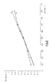
- Fig. 6 shows the variation in measured total current (ie z) versus force applied to an area of tablet 1.5 millimetres square. It can be seen that this too would benefit from some digital processing, since the line produced is not as straight as ideally it should be. This would be straight forward to achieve if necessary, for example by employing a look-up table correlating measured current to applied pressure. It will be noted that below a certain non-zero value for the pressure the measured total current is zero. This is useful since it means that light pressure (eg from a person's hand) will not be detected by the tablet and will not interfere with the normal operation of the tablet.
- the variation in current with applied pressure stems from 2 effects.
- the first of these is that the resistive material compresses locally, so reducing the electrical resistance in the region of applied pressure since the fibres in the material are in better electrical contact.
- the second and more significant effect is that the contact area between the conductive and resistive layers increases.
- the increase in contact area with increased pressure can cause the measured position to be in error. This happens when the pressure is applied significantly closer to one contact pad than to the opposed contact pad (eg closer to 16 than to 17).
- the increase in contact area with pressure is uniform in all directions but since the contact area is closer to 16 than to 17, the distance from the contact area edge to 16 reduces by a greater percentage than the distance from the contact area edge to 17. This causes the measured position to appear further towards the near edge as more pressure is applied. If this effect is unacceptable then it would be necessary to compensate for it digitally in the computer by weighting the position measurement towards the centre, the level of weighting increasing with increasing pressure (ie increasing total current).
- Another compensation which may be required is to allow for the fact that, at a constant pressure, the total current increases as the contact point approaches any edge of the tablet. This is because the overall resistance through the resistive sheet from the contact point to the contact pads 16, 17, 23, 24 decreases as the contact point moves further from the centre and closer to 1 or 2 of the contact pads. If this effect is too large to be ignored then a suitable weighting could be applied when the data is processed.
- the rate at which the location and pressure of the stylus are sampled will depend on the requirements of the application and the circuitry and computer software employed. For graphics input to a terminal and for signature verification a sampling rate of around 10 kHz may be acceptable although a rate of around 20 kHz is preferable.
Abstract
Description
- This invention relates to a graphics input tablet. The invention is particularly useful in the data processing field where it may be employed to input data of a graphical nature into a data processing machine.
- In the data processing field one of the major problems to users of a system is the rapid inputting of data. This has traditionally been achieved with a keyboard but when it is necessary to input graphical data, rather than character strings, a keyboard is grossly inefficient. There are various examples in the prior art of attempts to provide a more efficient and easier to use input means for graphical data.
- One such example is disclosed in EP 5,996 (Quest Automation Ltd.) which shows an electrographic apparatus with two resistive layers, one overlying the other, held apart by a framework but arranged to be brought into contact by the pressure of a stylus or similar. Excitation voltages are applied to the resistive layer at 90 degrees to each other and two analogue voltages related to the position of the stylus are obtained in an unspecified manner.
- Another example is disclosed in GB 2,088,063 (Robert Branton). This shows a conductive layer overlying a rectangular resistive layer with an insulating mesh between the two. The resistive layer has a contact at each corner and one opposed pair of contacts is energised at any one time. A stylus (ball-point pen or similar) is pressed onto the upper, conductive layer which then makes contact, through a gap in the insulating mesh, with the resistive layer. In consequence, the potential of the conductive layer equals that of the resistive layer at the point of contact; since this varies with the relative distances of the point from each of the polarised contacts, the potential of the conductive layer provides information to identify the position of the stylus. Once the position with respect to these polarised contacts is established they are de-energised and the other pair is polarised to give information regarding the position of the stylus along a different axis. Thus the position of the stylus in 2 dimensions may be identified.
- The prior art techniques only permit 2 dimensional input directly from the tablet; if a third dimension is required it must be input by other means eg a potentiometer arranged for manual control. The ability to input 3 dimensional data using the tablet alone would be very useful, for example a) to define the colour and/or intensity of a location on a graphic terminal or b) for signature verification where the profile of the pressure applied across the signature would be a useful additional check, above and beyond a 2 dimensional check of the appearance of the signature. Further, the prior art techniques do not permit the pressure information to be detected at all; this information could be useful, for example in the case of a one dimensional position-detecting tablet in the form of a strip. This would provide 2 dimensional input capability without occupying the large area taken up by a prior art 2-d input tablet.
- Accordingly, the present invention provides a graphics input tablet comprising a layer of electrically resistive material supported coextensively with a layer of electrically conductive material to provide a flat tablet surface, first and second conductors connected respectively to first and second portions of the resistive layer, said portions being spaced apart on a notional first line across the tablet surface, characterised in that when an electrical potential is applied between the resistive layer and the conductive layer and localised pressure is applied to the tablet surface, currents flow from said first and second conductors through the resistive layer to the conductive layer, the relative magnitudes of these currents being related to the respective distances of the region of applied pressure from the first and second portions, the resistive material has the property that the electrical resistance between the layers in the region of the localised pressure applied thereto changes monotonically with the applied pressure and when the localised pressure is applied, the total current flowing between the resistive sheet and the conductive sheet is related to the magnitude of the applied pressure.
- This provides the facility to detect the position of a stylus in two dimensions, ie one linear dimension and one pressure dimension.
- Preferably, the graphics input tablet further comprises third and fourth conductors connected respectively to third and fourth portions of the resistive layer, said portions being spaced apart on a second notional line, intersecting said first notional line, across the tablet surface, such that when said localised pressure is applied in said region currents flow in said third and fourth conductors, the relative magnitudes of the currents in the third and fourth conductors being related to the respective distances of said third and fourth portions from the area of applied localised pressure.
- This provides the facility to detect the position of a stylus in 3 dimensions, ie two linear dimensions and one pressure dimension.
- Preferably, the graphics input tablet has electrical sensing means arranged to evaluate said total current by summing the individual currents measured in each of said conductors.
- Alternatively, the graphics input tablet has electrical sensing means arranged to evaluate said total current from a measurement of the current flowing between the electrical excitation means and the conductive layer.
- The resistive layer may be in the form of a single sheet of material. Alternatively, the resistive layer may comprise two sheets, each of a resistive material, the conductors being connected to a first of said sheets and the second of said sheets having the property as aforesaid that the electrical resistance between the layers in the region of localised pressure applied thereto changes monotonically with the magnitude of the pressure applied to the layers.
-
- Fig. 1a shows schematically a cross-section through a graphics input tablet according to the present invention.
- Fig. 1b shows schematically a cross-section through an alternative embodiment of a graphics input tablet according to the present invention.
- Fig. 2 shows schematically a plan view of the tablet of Fig. 1a.
- Fig. 3a shows schematically a circuit for processing signals representing positional and pressure information produced by the present invention.
- Fig. 3b shows schematically a circuit for inputting the outputs of the circuit of Fig. 3a into a computer.
- Fig. 4 shows schematically an alternative circuit for processing signals representing positional and pressure information produced by the present invention and inputting this into a computer.
- Fig. 5 is a schematic graph showing variations in positional measurements versus actual position when employing the present invention.
- Fig. 6 is a schematic graph showing variations in measured total current versus actual force applied to a small area using the present invention.
- Fig. 1a shows a graphics input tablet according to the present invention.
Layer 10 is a compressible resistive sheet known as Vermahide (Trade Mark). This material has the property that its localised electrical resistance reduces with increased pressure exerted on it as the electrically conducting fibres which make it up are forced into more intimate contact. Beneathlayer 10 islayer 11 which is an electrically conducting coat applied to insulatingsubstrate 13. Beneathinsulating substrate 13 isconductive coat 50 which may be electrically grounded to give electrostatic screening.Layers layers protective sheet 12 which is electrically insulating, physically hard-wearing and yet locally elastically deformable. Electrical connection is made toconductive layer 11 byconductor 30 and to opposed edges ofresistive layer 10 byconductors - Fig. 1b shows an alternative tablet comprising two resistive sheets, one compressible 10a and one rigid 10b.
Conductive layer 11 overlies the resistive sheets and is locally elastically deformable. - Fig. 2 shows a plan view of the tablet in Fig. 1a. Contact
pads conductors remainder 20 oflayer 10 as the input region where a user applies localised pressure with a stylus, causing currents to flow inconductors - Fig. 3a shows one technique for producing signals x, y, z representing the position of pressure applied on region 20 (x, y) and the magnitude of pressure applied (z). Four current sense amplifiers (44) are provided for measuring the current flowing in the
conductors circuits conductors conductors dividers opposed conductors 14, 15 (or 21, 22); rather, if current in 14 = I1 and current in 15 = I2 then the value of x is:
x =
- This function is selected since it provides a result which varies approximately rectilinearly between 0 and 1.
- The signal for z, representing the pressure applied by the stylus is simply a sum of the individual currents in
conductors - Fig. 3b shows a circuit for inputting x, y and z to a computer. The
multiplexer 40 selects each of x, y, z in turn to forward to the analogue todigital convertor 41. The results are fed to buffer 42 and thence todata bus 43 which is connected to the computer. - Fig. 4 shows an alternative arrangement to that of Figs. 3a, 3b. In this case there is an additional
current sense amplifier 45 for directly measuring the current inconductor 30. This avoids the expense and inaccuracy of analogue summing circuit 39 (used in conjunction with 35 and 37). Further, the generation of the x and y functions is performed in the computer so the tablet does not need the local intelligence provided bycircuits circuits - In use, the
conductive layer 11 of the tablet is held at a voltage equal to -10 Volts. Theconductors resistive layer 10 are held at 0 Volts. When no pressure is applied to the upper surface of the tablet the physical contact betweenlayers layers conductive layer 11 to theconductors resistive layer 10. The current through each of these conductors is in inverse relation to the distance from the respective contact pad to the point where pressure is applied. - Another possibility is to have the arrangement as shown in Fig. 4 but without sense amplifier 45 (and its associated resistor). In this case the computer must sum all four conductor currents digitally. This is a processing overhead which reduces the maximum sampling rate but the hardware will be still cheaper to produce.
- Fig. 5 shows the variation in the measured value of x versus the actual position at which pressure is applied. It can be seen that there are significant edge effects which mean that it may be necessary to process digitally the measurements once they are received by the computer in order to expand the measured x values to cover the entire range from 0 to 1 (0 is the left-hand edge of
area - Fig. 6 shows the variation in measured total current (ie z) versus force applied to an area of tablet 1.5 millimetres square. It can be seen that this too would benefit from some digital processing, since the line produced is not as straight as ideally it should be. This would be straight forward to achieve if necessary, for example by employing a look-up table correlating measured current to applied pressure. It will be noted that below a certain non-zero value for the pressure the measured total current is zero. This is useful since it means that light pressure (eg from a person's hand) will not be detected by the tablet and will not interfere with the normal operation of the tablet.
- The variation in current with applied pressure stems from 2 effects. The first of these is that the resistive material compresses locally, so reducing the electrical resistance in the region of applied pressure since the fibres in the material are in better electrical contact. The second and more significant effect is that the contact area between the conductive and resistive layers increases.
- The increase in contact area with increased pressure can cause the measured position to be in error. This happens when the pressure is applied significantly closer to one contact pad than to the opposed contact pad (eg closer to 16 than to 17). The increase in contact area with pressure is uniform in all directions but since the contact area is closer to 16 than to 17, the distance from the contact area edge to 16 reduces by a greater percentage than the distance from the contact area edge to 17. This causes the measured position to appear further towards the near edge as more pressure is applied. If this effect is unacceptable then it would be necessary to compensate for it digitally in the computer by weighting the position measurement towards the centre, the level of weighting increasing with increasing pressure (ie increasing total current).
- Another compensation which may be required is to allow for the fact that, at a constant pressure, the total current increases as the contact point approaches any edge of the tablet. This is because the overall resistance through the resistive sheet from the contact point to the
contact pads - The rate at which the location and pressure of the stylus are sampled will depend on the requirements of the application and the circuitry and computer software employed. For graphics input to a terminal and for signature verification a sampling rate of around 10 kHz may be acceptable although a rate of around 20 kHz is preferable.
Claims (10)
a layer of electrically resistive material (10) supported coextensively with a layer of electrically conductive material (11) to provide a flat tablet surface,
first and second conductors (14, 15) connected respectively to first and second portions of the resistive layer (18, 19), said portions being spaced apart on a notional first line across the tablet surface,
characterised in that:
when an electrical potential is applied between the resistive layer and the conductive layer and localised pressure is applied to the tablet surface, currents flow from said first and second conductors through the resistive layer to the conductive layer, the relative magnitudes of these currents being related to the respective distances of the region of applied pressure from the first and second portions,
the resistive material has the property that the electrical resistance between the layers in the region of the localised pressure applied thereto changes monotonically with the applied pressure and
when the localised pressure is applied, the total current flowing between the resistive sheet and the conductive sheet is related to the magnitude of the applied pressure.
Applications Claiming Priority (2)
| Application Number | Priority Date | Filing Date | Title |
|---|---|---|---|
| GB8710033 | 1987-04-28 | ||
| GB8710033A GB2204131B (en) | 1987-04-28 | 1987-04-28 | Graphics input tablet |
Publications (3)
| Publication Number | Publication Date |
|---|---|
| EP0288692A2 true EP0288692A2 (en) | 1988-11-02 |
| EP0288692A3 EP0288692A3 (en) | 1990-01-24 |
| EP0288692B1 EP0288692B1 (en) | 1993-07-14 |
Family
ID=10616483
Family Applications (1)
| Application Number | Title | Priority Date | Filing Date |
|---|---|---|---|
| EP88103374A Expired - Lifetime EP0288692B1 (en) | 1987-04-28 | 1988-03-04 | Graphics input tablet |
Country Status (6)
| Country | Link |
|---|---|
| US (1) | US4798919A (en) |
| EP (1) | EP0288692B1 (en) |
| JP (1) | JPS63276117A (en) |
| CA (1) | CA1297177C (en) |
| DE (1) | DE3882268T2 (en) |
| GB (1) | GB2204131B (en) |
Cited By (24)
| Publication number | Priority date | Publication date | Assignee | Title |
|---|---|---|---|---|
| EP0350638A2 (en) * | 1988-07-14 | 1990-01-17 | Blomberg Robotertechnik GmbH | Tactile sensor |
| FR2683649A1 (en) * | 1991-11-13 | 1993-05-14 | Iee Sarl | Digitising tablet |
| US5369228A (en) * | 1991-11-30 | 1994-11-29 | Signagraphics Corporation | Data input device with a pressure-sensitive input surface |
| EP0718750A1 (en) * | 1994-12-22 | 1996-06-26 | Nokia Mobile Phones Ltd. | Information transfer method using a pointing device |
| GB2383419A (en) * | 2001-12-21 | 2003-06-25 | Motorola Inc | Multilayer resistive digitiser structure |
| US6888536B2 (en) * | 1998-01-26 | 2005-05-03 | The University Of Delaware | Method and apparatus for integrating manual input |
| WO2005043375A2 (en) * | 2003-10-08 | 2005-05-12 | 3M Innovative Properties Company | Resistive touch screen incorporating conductive polymer |
| US8416209B2 (en) | 2004-05-06 | 2013-04-09 | Apple Inc. | Multipoint touchscreen |
| US8432371B2 (en) | 2006-06-09 | 2013-04-30 | Apple Inc. | Touch screen liquid crystal display |
| US8493330B2 (en) | 2007-01-03 | 2013-07-23 | Apple Inc. | Individual channel phase delay scheme |
| US8552989B2 (en) | 2006-06-09 | 2013-10-08 | Apple Inc. | Integrated display and touch screen |
| US8654083B2 (en) | 2006-06-09 | 2014-02-18 | Apple Inc. | Touch screen liquid crystal display |
| US8743300B2 (en) | 2010-12-22 | 2014-06-03 | Apple Inc. | Integrated touch screens |
| US9606668B2 (en) | 2002-02-07 | 2017-03-28 | Apple Inc. | Mode-based graphical user interfaces for touch sensitive input devices |
| US9710095B2 (en) | 2007-01-05 | 2017-07-18 | Apple Inc. | Touch screen stack-ups |
| US9785258B2 (en) | 2003-09-02 | 2017-10-10 | Apple Inc. | Ambidextrous mouse |
| US9983742B2 (en) | 2002-07-01 | 2018-05-29 | Apple Inc. | Electronic device having display and surrounding touch sensitive bezel for user interface and control |
| US10248221B2 (en) | 2009-08-17 | 2019-04-02 | Apple Inc. | Housing as an I/O device |
| US10338789B2 (en) | 2004-05-06 | 2019-07-02 | Apple Inc. | Operation of a computer with touch screen interface |
| US10915207B2 (en) | 2006-05-02 | 2021-02-09 | Apple Inc. | Multipoint touch surface controller |
| US10990183B2 (en) | 2010-04-05 | 2021-04-27 | Tactile Displays, Llc | Interactive display with tactile feedback |
| US10990184B2 (en) | 2010-04-13 | 2021-04-27 | Tactile Displays, Llc | Energy efficient interactive display with energy regenerative keyboard |
| US11036282B2 (en) | 2004-07-30 | 2021-06-15 | Apple Inc. | Proximity detector in handheld device |
| US11275405B2 (en) | 2005-03-04 | 2022-03-15 | Apple Inc. | Multi-functional hand-held device |
Families Citing this family (123)
| Publication number | Priority date | Publication date | Assignee | Title |
|---|---|---|---|---|
| US5159159A (en) * | 1990-12-07 | 1992-10-27 | Asher David J | Touch sensor and controller |
| JP2516502B2 (en) * | 1991-09-25 | 1996-07-24 | 日本写真印刷株式会社 | Input device |
| US5550330A (en) * | 1991-10-16 | 1996-08-27 | Fanuc Limited | Digitizing control apparatus |
| US5262777A (en) * | 1991-11-16 | 1993-11-16 | Sri International | Device for generating multidimensional input signals to a computer |
| US5335557A (en) * | 1991-11-26 | 1994-08-09 | Taizo Yasutake | Touch sensitive input control device |
| USRE40891E1 (en) | 1991-11-26 | 2009-09-01 | Sandio Technology Corp. | Methods and apparatus for providing touch-sensitive input in multiple degrees of freedom |
| US6597347B1 (en) | 1991-11-26 | 2003-07-22 | Itu Research Inc. | Methods and apparatus for providing touch-sensitive input in multiple degrees of freedom |
| US5451724A (en) * | 1992-08-05 | 1995-09-19 | Fujitsu Limited | Touch panel for detecting a coordinate of an arbitrary position where pressure is applied |
| KR200151013Y1 (en) * | 1993-04-20 | 1999-07-15 | 손욱 | Digitizer |
| JP3201874B2 (en) * | 1993-04-23 | 2001-08-27 | エスエムケイ株式会社 | Method and apparatus for detecting coordinates of resistance pressure-sensitive tablet |
| US5731804A (en) * | 1995-01-18 | 1998-03-24 | Immersion Human Interface Corp. | Method and apparatus for providing high bandwidth, low noise mechanical I/O for computer systems |
| US5805140A (en) * | 1993-07-16 | 1998-09-08 | Immersion Corporation | High bandwidth force feedback interface using voice coils and flexures |
| US5767839A (en) * | 1995-01-18 | 1998-06-16 | Immersion Human Interface Corporation | Method and apparatus for providing passive force feedback to human-computer interface systems |
| US5739811A (en) * | 1993-07-16 | 1998-04-14 | Immersion Human Interface Corporation | Method and apparatus for controlling human-computer interface systems providing force feedback |
| US5724264A (en) * | 1993-07-16 | 1998-03-03 | Immersion Human Interface Corp. | Method and apparatus for tracking the position and orientation of a stylus and for digitizing a 3-D object |
| US6437771B1 (en) * | 1995-01-18 | 2002-08-20 | Immersion Corporation | Force feedback device including flexure member between actuator and user object |
| US5721566A (en) | 1995-01-18 | 1998-02-24 | Immersion Human Interface Corp. | Method and apparatus for providing damping force feedback |
| US5734373A (en) * | 1993-07-16 | 1998-03-31 | Immersion Human Interface Corporation | Method and apparatus for controlling force feedback interface systems utilizing a host computer |
| US5466895A (en) * | 1994-01-07 | 1995-11-14 | Microtouch Systems, Inc. | Wear resistant improved tablet for a digitizer |
| US6850222B1 (en) | 1995-01-18 | 2005-02-01 | Immersion Corporation | Passive force feedback for computer interface devices |
| US5691898A (en) * | 1995-09-27 | 1997-11-25 | Immersion Human Interface Corp. | Safe and low cost computer peripherals with force feedback for consumer applications |
| US7113166B1 (en) | 1995-06-09 | 2006-09-26 | Immersion Corporation | Force feedback devices using fluid braking |
| US6166723A (en) * | 1995-11-17 | 2000-12-26 | Immersion Corporation | Mouse interface device providing force feedback |
| US6697748B1 (en) * | 1995-08-07 | 2004-02-24 | Immersion Corporation | Digitizing system and rotary table for determining 3-D geometry of an object |
| US5959613A (en) | 1995-12-01 | 1999-09-28 | Immersion Corporation | Method and apparatus for shaping force signals for a force feedback device |
| US5825308A (en) | 1996-11-26 | 1998-10-20 | Immersion Human Interface Corporation | Force feedback interface having isotonic and isometric functionality |
| US6100874A (en) | 1995-11-17 | 2000-08-08 | Immersion Corporation | Force feedback mouse interface |
| US6704001B1 (en) * | 1995-11-17 | 2004-03-09 | Immersion Corporation | Force feedback device including actuator with moving magnet |
| US7027032B2 (en) * | 1995-12-01 | 2006-04-11 | Immersion Corporation | Designing force sensations for force feedback computer applications |
| US8508469B1 (en) | 1995-12-01 | 2013-08-13 | Immersion Corporation | Networked applications including haptic feedback |
| US6028593A (en) * | 1995-12-01 | 2000-02-22 | Immersion Corporation | Method and apparatus for providing simulated physical interactions within computer generated environments |
| US6147674A (en) | 1995-12-01 | 2000-11-14 | Immersion Corporation | Method and apparatus for designing force sensations in force feedback computer applications |
| US6219032B1 (en) * | 1995-12-01 | 2001-04-17 | Immersion Corporation | Method for providing force feedback to a user of an interface device based on interactions of a controlled cursor with graphical elements in a graphical user interface |
| US6859819B1 (en) | 1995-12-13 | 2005-02-22 | Immersion Corporation | Force feedback enabled over a computer network |
| US6078308A (en) * | 1995-12-13 | 2000-06-20 | Immersion Corporation | Graphical click surfaces for force feedback applications to provide user selection using cursor interaction with a trigger position within a boundary of a graphical object |
| US5940065A (en) | 1996-03-15 | 1999-08-17 | Elo Touchsystems, Inc. | Algorithmic compensation system and method therefor for a touch sensor panel |
| US6054979A (en) * | 1996-08-21 | 2000-04-25 | Compaq Computer Corporation | Current sensing touchpad for computers and the like |
| US6686911B1 (en) * | 1996-11-26 | 2004-02-03 | Immersion Corporation | Control knob with control modes and force feedback |
| US7489309B2 (en) * | 1996-11-26 | 2009-02-10 | Immersion Corporation | Control knob with multiple degrees of freedom and force feedback |
| GB9722766D0 (en) | 1997-10-28 | 1997-12-24 | British Telecomm | Portable computers |
| US7844914B2 (en) | 2004-07-30 | 2010-11-30 | Apple Inc. | Activating virtual keys of a touch-screen virtual keyboard |
| US9292111B2 (en) | 1998-01-26 | 2016-03-22 | Apple Inc. | Gesturing with a multipoint sensing device |
| US9239673B2 (en) | 1998-01-26 | 2016-01-19 | Apple Inc. | Gesturing with a multipoint sensing device |
| US6369804B1 (en) | 1998-09-26 | 2002-04-09 | Eleksen Limited | Detector constructed from fabric having non-uniform conductivity |
| GB0007679D0 (en) * | 2000-03-30 | 2000-05-17 | Electrotextiles Comp Ltd | Data input device |
| US6333736B1 (en) | 1999-05-20 | 2001-12-25 | Electrotextiles Company Limited | Detector constructed from fabric |
| US6452479B1 (en) | 1999-05-20 | 2002-09-17 | Eleksen Limited | Detector contructed from fabric |
| US6861961B2 (en) * | 2000-03-30 | 2005-03-01 | Electrotextiles Company Limited | Foldable alpha numeric keyboard |
| JP2003529837A (en) * | 2000-03-30 | 2003-10-07 | エレクセン・リミテッド | Manual input device and processor |
| GB2365134A (en) * | 2000-03-30 | 2002-02-13 | Electrotextiles Co Ltd | Detector constructed from electrically conducting fabric |
| AU770743B2 (en) * | 2000-04-03 | 2004-03-04 | Intelligent Textiles Limited | Conductive pressure sensitive textile |
| US6909354B2 (en) * | 2001-02-08 | 2005-06-21 | Interlink Electronics, Inc. | Electronic pressure sensitive transducer apparatus and method for manufacturing same |
| US7030861B1 (en) | 2001-02-10 | 2006-04-18 | Wayne Carl Westerman | System and method for packing multi-touch gestures onto a hand |
| US7567232B2 (en) | 2001-03-09 | 2009-07-28 | Immersion Corporation | Method of using tactile feedback to deliver silent status information to a user of an electronic device |
| DE10122634A1 (en) * | 2001-05-10 | 2002-11-14 | Bs Biometric Systems Gmbh | Tray especially graphics tablet |
| US20070085841A1 (en) * | 2001-10-22 | 2007-04-19 | Apple Computer, Inc. | Method and apparatus for accelerated scrolling |
| US7312785B2 (en) | 2001-10-22 | 2007-12-25 | Apple Inc. | Method and apparatus for accelerated scrolling |
| US7345671B2 (en) | 2001-10-22 | 2008-03-18 | Apple Inc. | Method and apparatus for use of rotational user inputs |
| US7046230B2 (en) * | 2001-10-22 | 2006-05-16 | Apple Computer, Inc. | Touch pad handheld device |
| JP2005514681A (en) * | 2001-10-23 | 2005-05-19 | イマージョン コーポレーション | Method of using haptic feedback by communicating a static state to a user of an electronic device |
| US8788253B2 (en) * | 2001-10-30 | 2014-07-22 | Immersion Corporation | Methods and apparatus for providing haptic feedback in interacting with virtual pets |
| JP4149926B2 (en) * | 2001-11-01 | 2008-09-17 | イマージョン コーポレーション | Method and apparatus for providing a tactile sensation |
| US7535454B2 (en) | 2001-11-01 | 2009-05-19 | Immersion Corporation | Method and apparatus for providing haptic feedback |
| US7333092B2 (en) * | 2002-02-25 | 2008-02-19 | Apple Computer, Inc. | Touch pad for handheld device |
| US7769417B2 (en) * | 2002-12-08 | 2010-08-03 | Immersion Corporation | Method and apparatus for providing haptic feedback to off-activating area |
| US7050045B2 (en) * | 2003-01-07 | 2006-05-23 | Interlink Electronics, Inc. | Miniature highly manufacturable mouse pointing device |
| EP1469378A1 (en) * | 2003-04-16 | 2004-10-20 | IEE INTERNATIONAL ELECTRONICS & ENGINEERING S.A. | Position detection apparatus |
| US20060181517A1 (en) * | 2005-02-11 | 2006-08-17 | Apple Computer, Inc. | Display actuator |
| US20070152977A1 (en) * | 2005-12-30 | 2007-07-05 | Apple Computer, Inc. | Illuminated touchpad |
| US7499040B2 (en) * | 2003-08-18 | 2009-03-03 | Apple Inc. | Movable touch pad with added functionality |
| US7495659B2 (en) * | 2003-11-25 | 2009-02-24 | Apple Inc. | Touch pad for handheld device |
| US8059099B2 (en) * | 2006-06-02 | 2011-11-15 | Apple Inc. | Techniques for interactive input to portable electronic devices |
| GB0404419D0 (en) | 2004-02-27 | 2004-03-31 | Intelligent Textiles Ltd | Electrical components and circuits constructed as textiles |
| US7653883B2 (en) | 2004-07-30 | 2010-01-26 | Apple Inc. | Proximity detector in handheld device |
| CN100555200C (en) | 2004-08-16 | 2009-10-28 | 苹果公司 | The method of the spatial resolution of touch sensitive devices and raising touch sensitive devices |
| US7671837B2 (en) * | 2005-09-06 | 2010-03-02 | Apple Inc. | Scrolling input arrangements using capacitive sensors on a flexible membrane |
| US7880729B2 (en) * | 2005-10-11 | 2011-02-01 | Apple Inc. | Center button isolation ring |
| US20070152983A1 (en) | 2005-12-30 | 2007-07-05 | Apple Computer, Inc. | Touch pad with symbols based on mode |
| US7538760B2 (en) | 2006-03-30 | 2009-05-26 | Apple Inc. | Force imaging input device and system |
| US7978181B2 (en) | 2006-04-25 | 2011-07-12 | Apple Inc. | Keystroke tactility arrangement on a smooth touch surface |
| US8022935B2 (en) | 2006-07-06 | 2011-09-20 | Apple Inc. | Capacitance sensing electrode with integrated I/O mechanism |
| US8743060B2 (en) | 2006-07-06 | 2014-06-03 | Apple Inc. | Mutual capacitance touch sensing device |
| US9360967B2 (en) * | 2006-07-06 | 2016-06-07 | Apple Inc. | Mutual capacitance touch sensing device |
| US20080006454A1 (en) * | 2006-07-10 | 2008-01-10 | Apple Computer, Inc. | Mutual capacitance touch sensing device |
| US7573464B2 (en) * | 2006-07-20 | 2009-08-11 | Interlink Electronics, Inc. | Shape adaptable resistive touchpad |
| US7795553B2 (en) | 2006-09-11 | 2010-09-14 | Apple Inc. | Hybrid button |
| US20080088600A1 (en) * | 2006-10-11 | 2008-04-17 | Apple Inc. | Method and apparatus for implementing multiple push buttons in a user input device |
| US20080088597A1 (en) * | 2006-10-11 | 2008-04-17 | Apple Inc. | Sensor configurations in a user input device |
| US8274479B2 (en) * | 2006-10-11 | 2012-09-25 | Apple Inc. | Gimballed scroll wheel |
| US8482530B2 (en) * | 2006-11-13 | 2013-07-09 | Apple Inc. | Method of capacitively sensing finger position |
| KR101533465B1 (en) * | 2006-12-27 | 2015-07-02 | 임머숀 코퍼레이션 | Virtual detents through vibrotactile feedback |
| US9654104B2 (en) | 2007-07-17 | 2017-05-16 | Apple Inc. | Resistive force sensor with capacitive discrimination |
| US8683378B2 (en) | 2007-09-04 | 2014-03-25 | Apple Inc. | Scrolling techniques for user interfaces |
| WO2009032898A2 (en) * | 2007-09-04 | 2009-03-12 | Apple Inc. | Compact input device |
| US20090058801A1 (en) * | 2007-09-04 | 2009-03-05 | Apple Inc. | Fluid motion user interface control |
| US20090073130A1 (en) * | 2007-09-17 | 2009-03-19 | Apple Inc. | Device having cover with integrally formed sensor |
| US8416198B2 (en) | 2007-12-03 | 2013-04-09 | Apple Inc. | Multi-dimensional scroll wheel |
| US8125461B2 (en) * | 2008-01-11 | 2012-02-28 | Apple Inc. | Dynamic input graphic display |
| US8820133B2 (en) * | 2008-02-01 | 2014-09-02 | Apple Inc. | Co-extruded materials and methods |
| US9454256B2 (en) | 2008-03-14 | 2016-09-27 | Apple Inc. | Sensor configurations of an input device that are switchable based on mode |
| US8665228B2 (en) | 2008-06-19 | 2014-03-04 | Tactile Displays, Llc | Energy efficient interactive display with energy regenerative keyboard |
| US8115745B2 (en) | 2008-06-19 | 2012-02-14 | Tactile Displays, Llc | Apparatus and method for interactive display with tactile feedback |
| US8217908B2 (en) | 2008-06-19 | 2012-07-10 | Tactile Displays, Llc | Apparatus and method for interactive display with tactile feedback |
| US9513705B2 (en) | 2008-06-19 | 2016-12-06 | Tactile Displays, Llc | Interactive display with tactile feedback |
| US20100058251A1 (en) * | 2008-08-27 | 2010-03-04 | Apple Inc. | Omnidirectional gesture detection |
| US8749495B2 (en) * | 2008-09-24 | 2014-06-10 | Immersion Corporation | Multiple actuation handheld device |
| US8816967B2 (en) | 2008-09-25 | 2014-08-26 | Apple Inc. | Capacitive sensor having electrodes arranged on the substrate and the flex circuit |
| US8500732B2 (en) * | 2008-10-21 | 2013-08-06 | Hermes Innovations Llc | Endometrial ablation devices and systems |
| US8395590B2 (en) * | 2008-12-17 | 2013-03-12 | Apple Inc. | Integrated contact switch and touch sensor elements |
| US9354751B2 (en) * | 2009-05-15 | 2016-05-31 | Apple Inc. | Input device with optimized capacitive sensing |
| US8872771B2 (en) * | 2009-07-07 | 2014-10-28 | Apple Inc. | Touch sensing device having conductive nodes |
| US8988191B2 (en) * | 2009-08-27 | 2015-03-24 | Symbol Technologies, Inc. | Systems and methods for pressure-based authentication of an input on a touch screen |
| JP5429814B2 (en) * | 2010-03-29 | 2014-02-26 | 株式会社ワコム | Indicator detection device and detection sensor |
| US8576171B2 (en) | 2010-08-13 | 2013-11-05 | Immersion Corporation | Systems and methods for providing haptic feedback to touch-sensitive input devices |
| US20120176328A1 (en) * | 2011-01-11 | 2012-07-12 | Egan Teamboard Inc. | White board operable by variable pressure inputs |
| CA2763271A1 (en) * | 2011-01-11 | 2012-07-11 | Egan Teamboard Inc. | Dimensionally stable white board |
| FR2971066B1 (en) | 2011-01-31 | 2013-08-23 | Nanotec Solution | THREE-DIMENSIONAL MAN-MACHINE INTERFACE. |
| US9582178B2 (en) | 2011-11-07 | 2017-02-28 | Immersion Corporation | Systems and methods for multi-pressure interaction on touch-sensitive surfaces |
| US9891709B2 (en) | 2012-05-16 | 2018-02-13 | Immersion Corporation | Systems and methods for content- and context specific haptic effects using predefined haptic effects |
| FR3002052B1 (en) | 2013-02-14 | 2016-12-09 | Fogale Nanotech | METHOD AND DEVICE FOR NAVIGATING A DISPLAY SCREEN AND APPARATUS COMPRISING SUCH A NAVIGATION |
| US9904394B2 (en) | 2013-03-13 | 2018-02-27 | Immerson Corporation | Method and devices for displaying graphical user interfaces based on user contact |
| US9547366B2 (en) | 2013-03-14 | 2017-01-17 | Immersion Corporation | Systems and methods for haptic and gesture-driven paper simulation |
| EP3341511B1 (en) | 2015-12-18 | 2019-08-21 | Intelligent Textiles Limited | Conductive fabric, method of manufacturing a conductive fabric and apparatus therefor |
Citations (4)
| Publication number | Priority date | Publication date | Assignee | Title |
|---|---|---|---|---|
| JPS58191089A (en) * | 1982-04-30 | 1983-11-08 | Toyo Commun Equip Co Ltd | Position detecting method |
| JPS5985583A (en) * | 1982-11-08 | 1984-05-17 | Nippon Telegr & Teleph Corp <Ntt> | Tablet |
| US4575580A (en) * | 1984-04-06 | 1986-03-11 | Astec International, Ltd. | Data input device with a circuit responsive to stylus up/down position |
| EP0194861A2 (en) * | 1985-03-11 | 1986-09-17 | Elographics, Inc. | Electrographic touch sensor with z-axis capability |
Family Cites Families (1)
| Publication number | Priority date | Publication date | Assignee | Title |
|---|---|---|---|---|
| JPS6029965B2 (en) * | 1982-03-10 | 1985-07-13 | 日本電信電話株式会社 | Graphic input device |
-
1987
- 1987-04-28 GB GB8710033A patent/GB2204131B/en not_active Expired - Fee Related
-
1988
- 1988-03-04 EP EP88103374A patent/EP0288692B1/en not_active Expired - Lifetime
- 1988-03-04 DE DE88103374T patent/DE3882268T2/en not_active Expired - Fee Related
- 1988-03-11 US US07/166,957 patent/US4798919A/en not_active Expired - Lifetime
- 1988-03-17 JP JP63062114A patent/JPS63276117A/en active Granted
- 1988-04-14 CA CA000564186A patent/CA1297177C/en not_active Expired - Fee Related
Patent Citations (4)
| Publication number | Priority date | Publication date | Assignee | Title |
|---|---|---|---|---|
| JPS58191089A (en) * | 1982-04-30 | 1983-11-08 | Toyo Commun Equip Co Ltd | Position detecting method |
| JPS5985583A (en) * | 1982-11-08 | 1984-05-17 | Nippon Telegr & Teleph Corp <Ntt> | Tablet |
| US4575580A (en) * | 1984-04-06 | 1986-03-11 | Astec International, Ltd. | Data input device with a circuit responsive to stylus up/down position |
| EP0194861A2 (en) * | 1985-03-11 | 1986-09-17 | Elographics, Inc. | Electrographic touch sensor with z-axis capability |
Non-Patent Citations (3)
| Title |
|---|
| PATENT ABSTRACTS OF JAPAN, vol. 8, no. 202 (P-300)[1639], 14th September 1984; & JP-A-59 085 583 (NIPPON DENSHIN DENWA KOSHA) 17-05-1984 * |
| PATENT ABSTRACTS OF JAPAN, vol. 8, no. 38 (P-255)[1475], 18th February 1984; & JP-A-58 191 089 (TOUYOU TSUUSHINKI K.K.) 08-11-1983 * |
| SYSTEMS-COMPUTERS-CONTROL, vol. 13, no. 3, May-June 1982, pages 30-39, Silver Spring, Maryland, US; Y. SATO et al.: "A pressure-sensitive device for input of graphics" * |
Cited By (61)
| Publication number | Priority date | Publication date | Assignee | Title |
|---|---|---|---|---|
| EP0350638A2 (en) * | 1988-07-14 | 1990-01-17 | Blomberg Robotertechnik GmbH | Tactile sensor |
| EP0350638A3 (en) * | 1988-07-14 | 1990-09-26 | Blomberg Robotertechnik Gmbh | Tactile sensor |
| FR2683649A1 (en) * | 1991-11-13 | 1993-05-14 | Iee Sarl | Digitising tablet |
| US5369228A (en) * | 1991-11-30 | 1994-11-29 | Signagraphics Corporation | Data input device with a pressure-sensitive input surface |
| EP0718750A1 (en) * | 1994-12-22 | 1996-06-26 | Nokia Mobile Phones Ltd. | Information transfer method using a pointing device |
| US6002387A (en) * | 1994-12-22 | 1999-12-14 | Nokia Mobile Phones, Ltd. | System for transferring information between a pointer and a display interface |
| US6888536B2 (en) * | 1998-01-26 | 2005-05-03 | The University Of Delaware | Method and apparatus for integrating manual input |
| US9626032B2 (en) | 1998-01-26 | 2017-04-18 | Apple Inc. | Sensor arrangement for use with a touch sensor |
| US9804701B2 (en) | 1998-01-26 | 2017-10-31 | Apple Inc. | Contact tracking and identification module for touch sensing |
| GB2383419B (en) * | 2001-12-21 | 2004-07-07 | Motorola Inc | Display devices |
| GB2383419A (en) * | 2001-12-21 | 2003-06-25 | Motorola Inc | Multilayer resistive digitiser structure |
| US9606668B2 (en) | 2002-02-07 | 2017-03-28 | Apple Inc. | Mode-based graphical user interfaces for touch sensitive input devices |
| US9983742B2 (en) | 2002-07-01 | 2018-05-29 | Apple Inc. | Electronic device having display and surrounding touch sensitive bezel for user interface and control |
| US10474251B2 (en) | 2003-09-02 | 2019-11-12 | Apple Inc. | Ambidextrous mouse |
| US9785258B2 (en) | 2003-09-02 | 2017-10-10 | Apple Inc. | Ambidextrous mouse |
| US10156914B2 (en) | 2003-09-02 | 2018-12-18 | Apple Inc. | Ambidextrous mouse |
| WO2005043375A2 (en) * | 2003-10-08 | 2005-05-12 | 3M Innovative Properties Company | Resistive touch screen incorporating conductive polymer |
| WO2005043375A3 (en) * | 2003-10-08 | 2005-08-25 | 3M Innovative Properties Co | Resistive touch screen incorporating conductive polymer |
| US8605051B2 (en) | 2004-05-06 | 2013-12-10 | Apple Inc. | Multipoint touchscreen |
| US10338789B2 (en) | 2004-05-06 | 2019-07-02 | Apple Inc. | Operation of a computer with touch screen interface |
| US8872785B2 (en) | 2004-05-06 | 2014-10-28 | Apple Inc. | Multipoint touchscreen |
| US8928618B2 (en) | 2004-05-06 | 2015-01-06 | Apple Inc. | Multipoint touchscreen |
| US8982087B2 (en) | 2004-05-06 | 2015-03-17 | Apple Inc. | Multipoint touchscreen |
| US8416209B2 (en) | 2004-05-06 | 2013-04-09 | Apple Inc. | Multipoint touchscreen |
| US9035907B2 (en) | 2004-05-06 | 2015-05-19 | Apple Inc. | Multipoint touchscreen |
| US10908729B2 (en) | 2004-05-06 | 2021-02-02 | Apple Inc. | Multipoint touchscreen |
| US11604547B2 (en) | 2004-05-06 | 2023-03-14 | Apple Inc. | Multipoint touchscreen |
| US9454277B2 (en) | 2004-05-06 | 2016-09-27 | Apple Inc. | Multipoint touchscreen |
| US11036282B2 (en) | 2004-07-30 | 2021-06-15 | Apple Inc. | Proximity detector in handheld device |
| US11360509B2 (en) | 2005-03-04 | 2022-06-14 | Apple Inc. | Electronic device having display and surrounding touch sensitive surfaces for user interface and control |
| US11275405B2 (en) | 2005-03-04 | 2022-03-15 | Apple Inc. | Multi-functional hand-held device |
| US10921941B2 (en) | 2005-03-04 | 2021-02-16 | Apple Inc. | Electronic device having display and surrounding touch sensitive surfaces for user interface and control |
| US10386980B2 (en) | 2005-03-04 | 2019-08-20 | Apple Inc. | Electronic device having display and surrounding touch sensitive surfaces for user interface and control |
| US11853518B2 (en) | 2006-05-02 | 2023-12-26 | Apple Inc. | Multipoint touch surface controller |
| US10915207B2 (en) | 2006-05-02 | 2021-02-09 | Apple Inc. | Multipoint touch surface controller |
| US8552989B2 (en) | 2006-06-09 | 2013-10-08 | Apple Inc. | Integrated display and touch screen |
| US8451244B2 (en) | 2006-06-09 | 2013-05-28 | Apple Inc. | Segmented Vcom |
| US11175762B2 (en) | 2006-06-09 | 2021-11-16 | Apple Inc. | Touch screen liquid crystal display |
| US10191576B2 (en) | 2006-06-09 | 2019-01-29 | Apple Inc. | Touch screen liquid crystal display |
| US10976846B2 (en) | 2006-06-09 | 2021-04-13 | Apple Inc. | Touch screen liquid crystal display |
| US9575610B2 (en) | 2006-06-09 | 2017-02-21 | Apple Inc. | Touch screen liquid crystal display |
| US9268429B2 (en) | 2006-06-09 | 2016-02-23 | Apple Inc. | Integrated display and touch screen |
| US11886651B2 (en) | 2006-06-09 | 2024-01-30 | Apple Inc. | Touch screen liquid crystal display |
| US9244561B2 (en) | 2006-06-09 | 2016-01-26 | Apple Inc. | Touch screen liquid crystal display |
| US8654083B2 (en) | 2006-06-09 | 2014-02-18 | Apple Inc. | Touch screen liquid crystal display |
| US8432371B2 (en) | 2006-06-09 | 2013-04-30 | Apple Inc. | Touch screen liquid crystal display |
| US8493330B2 (en) | 2007-01-03 | 2013-07-23 | Apple Inc. | Individual channel phase delay scheme |
| US10521065B2 (en) | 2007-01-05 | 2019-12-31 | Apple Inc. | Touch screen stack-ups |
| US9710095B2 (en) | 2007-01-05 | 2017-07-18 | Apple Inc. | Touch screen stack-ups |
| US10739868B2 (en) | 2009-08-17 | 2020-08-11 | Apple Inc. | Housing as an I/O device |
| US11644865B2 (en) | 2009-08-17 | 2023-05-09 | Apple Inc. | Housing as an I/O device |
| US10248221B2 (en) | 2009-08-17 | 2019-04-02 | Apple Inc. | Housing as an I/O device |
| US10990183B2 (en) | 2010-04-05 | 2021-04-27 | Tactile Displays, Llc | Interactive display with tactile feedback |
| US10996762B2 (en) | 2010-04-05 | 2021-05-04 | Tactile Displays, Llc | Interactive display with tactile feedback |
| US10990184B2 (en) | 2010-04-13 | 2021-04-27 | Tactile Displays, Llc | Energy efficient interactive display with energy regenerative keyboard |
| US10409434B2 (en) | 2010-12-22 | 2019-09-10 | Apple Inc. | Integrated touch screens |
| US8743300B2 (en) | 2010-12-22 | 2014-06-03 | Apple Inc. | Integrated touch screens |
| US8804056B2 (en) | 2010-12-22 | 2014-08-12 | Apple Inc. | Integrated touch screens |
| US9025090B2 (en) | 2010-12-22 | 2015-05-05 | Apple Inc. | Integrated touch screens |
| US9146414B2 (en) | 2010-12-22 | 2015-09-29 | Apple Inc. | Integrated touch screens |
| US9727193B2 (en) | 2010-12-22 | 2017-08-08 | Apple Inc. | Integrated touch screens |
Also Published As
| Publication number | Publication date |
|---|---|
| JPS63276117A (en) | 1988-11-14 |
| CA1297177C (en) | 1992-03-10 |
| EP0288692B1 (en) | 1993-07-14 |
| DE3882268D1 (en) | 1993-08-19 |
| GB2204131B (en) | 1991-04-17 |
| GB8710033D0 (en) | 1987-06-03 |
| JPH0563815B2 (en) | 1993-09-13 |
| DE3882268T2 (en) | 1994-02-17 |
| US4798919A (en) | 1989-01-17 |
| GB2204131A (en) | 1988-11-02 |
| EP0288692A3 (en) | 1990-01-24 |
Similar Documents
| Publication | Publication Date | Title |
|---|---|---|
| US4798919A (en) | Graphics input tablet with three-dimensional data | |
| US10156949B2 (en) | Force-touch sensor with multilayered electrodes | |
| US5159159A (en) | Touch sensor and controller | |
| US4659874A (en) | X-Y position sensor | |
| CA1248195A (en) | System for sensing spatial coordinates | |
| JP3016455B2 (en) | Electromagnetic digitizer / tablet | |
| US5369228A (en) | Data input device with a pressure-sensitive input surface | |
| US4484026A (en) | Touch tablet data device | |
| US4456787A (en) | Electrographic system and method | |
| GB2046450A (en) | Apparatus for detecting x and y coordinates of input points | |
| US3624619A (en) | Pressure-sensing tablet | |
| US4523654A (en) | Electrographic system | |
| JPH0944289A (en) | Input pad system | |
| US4164622A (en) | Graphical input apparatus for electrical equipment | |
| US4990725A (en) | Device for locating the unknown position of an electrical conductor belonging to a set of separate conductors and a touch sensitive panel comprising such devices | |
| JPS5837783A (en) | Coordinate input device using conductive incorporated resistive film | |
| JPH0215895B2 (en) | ||
| US6151013A (en) | Electrical probe-position sensor | |
| JP3988569B2 (en) | Calligraphy input device | |
| JPS635075Y2 (en) | ||
| JPS5837782A (en) | Resistive film split type coordinate input device | |
| JPH0413719Y2 (en) | ||
| JPS58155487A (en) | Figure input device | |
| JPH0330901Y2 (en) | ||
| JPS5887675A (en) | Coordinate input device |
Legal Events
| Date | Code | Title | Description |
|---|---|---|---|
| PUAI | Public reference made under article 153(3) epc to a published international application that has entered the european phase |
Free format text: ORIGINAL CODE: 0009012 |
|
| AK | Designated contracting states |
Kind code of ref document: A2 Designated state(s): DE FR GB IT |
|
| 17P | Request for examination filed |
Effective date: 19890222 |
|
| PUAL | Search report despatched |
Free format text: ORIGINAL CODE: 0009013 |
|
| AK | Designated contracting states |
Kind code of ref document: A3 Designated state(s): DE FR GB IT |
|
| 17Q | First examination report despatched |
Effective date: 19910718 |
|
| GRAA | (expected) grant |
Free format text: ORIGINAL CODE: 0009210 |
|
| AK | Designated contracting states |
Kind code of ref document: B1 Designated state(s): DE FR GB IT |
|
| PG25 | Lapsed in a contracting state [announced via postgrant information from national office to epo] |
Ref country code: IT Free format text: LAPSE BECAUSE OF FAILURE TO SUBMIT A TRANSLATION OF THE DESCRIPTION OR TO PAY THE FEE WITHIN THE PRE;WARNING: LAPSES OF ITALIAN PATENTS WITH EFFECTIVE DATE BEFORE 2007 MAY HAVE OCCURRED AT ANY TIME BEFORE 2007. THE CORRECT EFFECTIVE DATE MAY BE DIFFERENT FROM THE ONE RECORDED.SCRIBED TIME-LIMIT Effective date: 19930714 |
|
| REF | Corresponds to: |
Ref document number: 3882268 Country of ref document: DE Date of ref document: 19930819 |
|
| ET | Fr: translation filed | ||
| PLBE | No opposition filed within time limit |
Free format text: ORIGINAL CODE: 0009261 |
|
| STAA | Information on the status of an ep patent application or granted ep patent |
Free format text: STATUS: NO OPPOSITION FILED WITHIN TIME LIMIT |
|
| 26N | No opposition filed | ||
| REG | Reference to a national code |
Ref country code: GB Ref legal event code: IF02 |
|
| PGFP | Annual fee paid to national office [announced via postgrant information from national office to epo] |
Ref country code: FR Payment date: 20020318 Year of fee payment: 15 |
|
| PGFP | Annual fee paid to national office [announced via postgrant information from national office to epo] |
Ref country code: GB Payment date: 20030303 Year of fee payment: 16 |
|
| PGFP | Annual fee paid to national office [announced via postgrant information from national office to epo] |
Ref country code: DE Payment date: 20030325 Year of fee payment: 16 |
|
| PG25 | Lapsed in a contracting state [announced via postgrant information from national office to epo] |
Ref country code: FR Free format text: LAPSE BECAUSE OF NON-PAYMENT OF DUE FEES Effective date: 20031127 |
|
| REG | Reference to a national code |
Ref country code: FR Ref legal event code: ST |
|
| PG25 | Lapsed in a contracting state [announced via postgrant information from national office to epo] |
Ref country code: GB Free format text: LAPSE BECAUSE OF NON-PAYMENT OF DUE FEES Effective date: 20040304 |
|
| PG25 | Lapsed in a contracting state [announced via postgrant information from national office to epo] |
Ref country code: DE Free format text: LAPSE BECAUSE OF NON-PAYMENT OF DUE FEES Effective date: 20041001 |
|
| GBPC | Gb: european patent ceased through non-payment of renewal fee |