EP0288739A2 - Method of self-aligning a trench isolation structure to an implanted well region - Google Patents
Method of self-aligning a trench isolation structure to an implanted well region Download PDFInfo
- Publication number
- EP0288739A2 EP0288739A2 EP88104638A EP88104638A EP0288739A2 EP 0288739 A2 EP0288739 A2 EP 0288739A2 EP 88104638 A EP88104638 A EP 88104638A EP 88104638 A EP88104638 A EP 88104638A EP 0288739 A2 EP0288739 A2 EP 0288739A2
- Authority
- EP
- European Patent Office
- Prior art keywords
- sidewall spacers
- masking layer
- substrate
- layer
- sidewall
- Prior art date
- Legal status (The legal status is an assumption and is not a legal conclusion. Google has not performed a legal analysis and makes no representation as to the accuracy of the status listed.)
- Withdrawn
Links
Images


Classifications
-
- H—ELECTRICITY
- H01—ELECTRIC ELEMENTS
- H01L—SEMICONDUCTOR DEVICES NOT COVERED BY CLASS H10
- H01L21/00—Processes or apparatus adapted for the manufacture or treatment of semiconductor or solid state devices or of parts thereof
- H01L21/02—Manufacture or treatment of semiconductor devices or of parts thereof
- H01L21/027—Making masks on semiconductor bodies for further photolithographic processing not provided for in group H01L21/18 or H01L21/34
- H01L21/033—Making masks on semiconductor bodies for further photolithographic processing not provided for in group H01L21/18 or H01L21/34 comprising inorganic layers
- H01L21/0334—Making masks on semiconductor bodies for further photolithographic processing not provided for in group H01L21/18 or H01L21/34 comprising inorganic layers characterised by their size, orientation, disposition, behaviour, shape, in horizontal or vertical plane
- H01L21/0337—Making masks on semiconductor bodies for further photolithographic processing not provided for in group H01L21/18 or H01L21/34 comprising inorganic layers characterised by their size, orientation, disposition, behaviour, shape, in horizontal or vertical plane characterised by the process involved to create the mask, e.g. lift-off masks, sidewalls, or to modify the mask, e.g. pre-treatment, post-treatment
-
- H—ELECTRICITY
- H01—ELECTRIC ELEMENTS
- H01L—SEMICONDUCTOR DEVICES NOT COVERED BY CLASS H10
- H01L21/00—Processes or apparatus adapted for the manufacture or treatment of semiconductor or solid state devices or of parts thereof
- H01L21/70—Manufacture or treatment of devices consisting of a plurality of solid state components formed in or on a common substrate or of parts thereof; Manufacture of integrated circuit devices or of parts thereof
- H01L21/71—Manufacture of specific parts of devices defined in group H01L21/70
- H01L21/76—Making of isolation regions between components
- H01L21/762—Dielectric regions, e.g. EPIC dielectric isolation, LOCOS; Trench refilling techniques, SOI technology, use of channel stoppers
- H01L21/76224—Dielectric regions, e.g. EPIC dielectric isolation, LOCOS; Trench refilling techniques, SOI technology, use of channel stoppers using trench refilling with dielectric materials
Definitions
- the present invention relates to a method of self-aligning a trench isolation structure to an implanted well region.
- VLSIC Very Large Scale Integrated Circuits
- isolation trench structures which are aligned to the perimeter of an implanted well region.
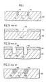
- Fig. 1 there is shown a cross sectional view of an implanted semiconductor device provided with isolation trench structures.
- the implanted well region 110 is a generic representation which represents a region utilized in any of numerous semiconductor devices, for example, a bipolar transistor, an FET transistor or a diode.
- the implanted well region 110 is a generic representation which represents a region utilized in any of numerous semiconductor devices, for example, a bipolar transistor, an FET transistor or a diode.
- isolation trenches 120 and 130 are filled with an insulator material 140.
- Each of the isolation trenches 120 or 130, filled with the insulator material 140 represents an isolation trench structure or barrier which isolates the implanted well region from neighboring implanted well regions or devices.
- Any of the insulator materials well known in the semiconductor art can be used, one suitable example being silicon dioxide.
- Fig. 1 represents an ideal arrangement; i.e., where the isolation trench structures are perfectly aligned to the perimeter of the implanted well region, and where the whole of the semiconductor substrate area between these isolation structures is efficiently doped at an optimum doping concentration.
- Figs. 2A-2C there is shown a prior art approach directed toward fabricating the above trench isolation arrangement.
- two maskings steps are utilized to fabricate the resulting structure.
- a first resist layer 210 is formed on the top surface of a semiconductor substrate body 200.
- the first resist layer 210 has been patterned in accordance with a first mask to provide an aperture 220 which is used to facilitate doping of the implanted well region 230 into the semiconductor substrate body 200.
- the first resist layer 210 is removed, and a second resist layer is formed on the top surface of the semiconductor substrate body 200.
- This second resist layer 240 as shown in Fig. 2B, is then patterned in accordance with a second mask to provide the trench apertures 250 and 260 which are used to etch isolation trenches 270 and 280 into the semiconductor substrate body 200.
- the second resist 240 is removed, and the isolation trenches 270 and 280 are filled with an insulator material 290.
- the result of these processing steps is an implanted well region 230 with corresponding isolation trench structures as shown in Fig. 2C.
- Figs. 2A-2C also illustrate shortcomings of this prior art approach.
- the first of these shortcomings results from the use of a two-mask approach.
- any misalignment of the first and second mask will result in misalignment of the isolation trench structures with the corresponding implanted well region.
- This misalignment is disadvantageous in at least two respects.
- a portion of the implanted well region 230 is caused to lie or stray outside the isolation region. This stray implantation may very well interfere with neighboring devices.
- Second, a portion of the isolation region is at a less than optimum doping concentration, thereby producing an inefficient use of semiconductor substrate area.
- there is a further inefficient use of semiconductor substrate area due to large widths of the isolation structures. This large width is caused by the limitations associated with using a photolithography masking technique to define the trench apertures.
- an object of the invention is to provide an improved processing approach which self-aligns a trench isolation structure to an implanted well region.
- An additional object of the present invention is to provide a trench isolation approach whereby the width of the isolation trenches is minimized.
- Still another object is to provide a trench isolation processing approach having a minimum of processing steps.
- a resist layer is patterned to provide an aperture to the semiconductor substrate body.
- a first conformal layer is then deposited and anisotropically etched to provide a sidewall spacer along the perimeter of the aperture.
- the smaller aperture defined between the sidewall spacers is then used as a window to implanted a well region into the semiconductor substrate body.
- a second conformal layer is then applied and anisotropically etched to provide second sidewall spacers along the perimeter of the smaller aperture.
- the resist layer is then removed, and an oxide layer is deposited to cover the sidewall spacers.
- a polishing process is applied to slowly remove the oxide layer to a point where the tops of the sidewall spacers are exposed.
- the sidewall spacers are then removed, and the resulting apertures are used to etch isolation trenches which are self-aligned to the implanted well region.
- the isolation trenches are filled with an insulator material to produce isolation trench structures that are self-aligned to the implanted well region.
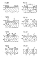
- Figs. 3A-3F there is shown a first processing approach of the present invention.
- the illustrated height, width and thickness dimensions are for the sake of example and clarity only, and are not intended to designate relative or actual dimensions; i.e., some dimensions may be exaggerated to improve the clarity of the illustrations. Examples of typical dimensions which are known will be revealed in the following description.
- a resist layer 310 is formed on top of a semiconductor substrate body 300.
- the resist layer 310 which can be composed of any well known photosensitive polymer (e.g. novolac resin), is patterned to provide a well aperture 320.
- a masking layer such as polyimide can be utilized as layer 310, in which case the aperture would be defined by a subsequently-applied photo resist layer.
- the well aperture 320 is then utilized to implant doping materials into the semiconductor substrate body 300 to define a well region (e.g. an N-type well region in a P-type substrate). While the implanted region is described as being a well region, in practice the implant could be utilized to form any diffusion region requiring isolation.
- the present invention does not utilize the two mask approach of the prior art. Instead, the present invention utilizes sidewall spacers on the original resist layer and aperture to provide alignment of the various semiconductor structures.
- sidewall spacers One example of using sidewall spacers is found in U.S. Patent No. 4,366,613, assigned to the assignee of this application, which discloses the construction of MOS Dynamic RAMs with a lightly doped drain.
- the present invention adds the further refinement of using an SIR approach to fabricate very narrow isolation trenches. Such trenches are desirable because the majority of semiconductor substrate area can now be devoted to the construction of semiconductor devices.
- a reference, which discusses an evaluation of trench isolation in CMOS devices is R.D. Rung, "Trench Isolation Prospects for Application in CMOS VLSI," 1984 IEDM Technical Digest pp. 574-577.
- a conformal layer 330 is formed over the entire surface of the semiconductor structure.
- Layer 330 should be "conformal" in the sense that the material is deposited with equal thickness on all exposed surfaces, and especially on the resist layer sidewalls 316 and 318.
- Any of the well known conformal deposition methods and materials can be used, for example, in a preferred embodiment, a nitride material is deposited by chemical vapor deposition (CVD).
- a critical point in the sidewall spacer approach is that the resist layer sidewalls 316 and 318 outlining the aperture 320 are used as vertical mandrels upon which a portion of the conformal layer is formed. Since “vertical” is a relative direction depending on the position which the semiconductor is held, the sidewalls or mandrels 316 and 318 are more accurately described as being perpendicular to the semiconductor substrate surface.
- the portions of the conformal layer 330 on the sidewalls 316 and 318 correspond to the mask which will be used to define the isolation trenches. Since the width of the isolation trenches to be formed will correspond exactly to the thickness of the conformal layer 330, this layer should be deposited to the thickness of the desired width of the isolation trenches.
- a nitride layer of 0.2 microns is suitable.
- an anisotropic etch is performed.
- the etch is "anisotropic" in the sense that the etch has a directional preference in attacking the horizontal portions of the conformal layer 330 while leaving vertical portions thereof undisturbed.
- the result of the anisotropic etching operation is shown in Fig. 3B. Note that the horizontal portions of the conformal layer 330, which were originally deposited on top of the resist layer 310 and within the well aperture 320, have been removed. Remaining are the sidewall spacers 322 and 324.
- sidewall image reversal we mean a process by which apertures are formed (in a masking structure) where the sidewall spacers are presently disposed. Because the sidewall spacers are narrow, the resulting openings in the masking structure will also be narrow.
- SIR approach for defining trench apertures by performing a sidewall image reversal process can be found in U.S. Patent No. 4,502,914, assigned to the assignee of this application, inventors Trumpp et al, the teachings of which are herein incorporated by reference.
- layer 340 is deposited on top of the semiconductor substrate body, as shown in Fig. 3C, so as to cover the vertical image portions 322 and 324.
- a planarization etch (preferably a polishing process) is then applied to the layer 340, to a point where the tops of the sidewall image portions 322 and 324 are polished or clipped off.
- This polishing step should be carried out in the presence of an abrasive slurry (e.g. Cab-O-Sil plus KOH), with a polishing pad pressure of approximately 0.965 bar.
- an etchant is employed which preferentially attacks the sidewall spacers without attacking the other surfaces.
- layer 340 is made up of silicon oxide. Hot H3PO4 will attack the nitride spacers without substantially attacking the surrounding oxide.
- Fig. 3D is an isolation trench mask structure having trench apertures 342 and 344 in perfect alignment with the implanted well region 335.
- the trench apertures 342 and 344 are then used to etch the isolation trenches 346 and 348 into the semiconductor substrate body 300.
- This etching process can be performed by well known semi-conductor etch methods, and in a preferred embodiment is carried out in a chlorine-based reactive ion etch (RIE).
- RIE reactive ion etch
- the air-filled isolation trenches may be a suitable isolation structure in some applications, in a preferred embodiment the isolation trenches 346 and 348 are filled with an insulator material 350, thereby resulting in the isolation arrangement shown in Fig. 3F.
- the isolation trench structures are self-aligned to the ends of the implanted well region 335.
- a processing approach may produce a shortcoming due to the lateral scattering of implanted ions. That is, as shown in Fig. 3A, during implantation, ions will scatter laterally with respect to the portion of the substrate exposed by resist opening 320, forming lateral diffusion regions 339 having low dopant concentrations. In Fig. 3F, note that these lateral portions 339 lie outside the isolated well region. Because the trench apertures 342 and 344 defined along the periphery of the well aperture 320 are used to vertically etch the isolation trenches 346 and 348 into the semiconductor substrate body, the portions 339 lying beyond the well aperture 320 were not removed. This result is disadvantageous in that the laterally scattered dopant outside the isolated region may interfere with neighboring devices.
- FIGs. 4A-4F illustrate an alternative processing approach which avoids this lateral scattering problem.
- structural elements which are the same as those of the first embodiment are designated by the same reference numerals or characters, and detailed descriptions thereof are omitted.
- the process for forming the implanted well region is delayed until after the conformal layer 330 as been anisotropically etched to define the sidewall spacers 322 and 324.
- the space 420 between the sidewall spacers 322 and 324 is used to define a narrow implanted well region 435.
- the implanted well region 435 has a peripheral region of lowered concentration 439 formed solely by laterally scattered dopants.
- these lateral diffusion areas 439 are disposed beneath the sidewall spacers 322 and 324, in contrast to being disposed under the resist layer 310 as shown in Fig. 3A.
- the remaining sidewall image reversal, trench etch and trench fill processing steps of Figs. 4C-4F exactly match those for Figs. 3C-3F, and the resulting isolated well device arrangement is shown in Fig. 4F.
- the processing approach of Figs. 4A-4F provides excellent alignment of the isolation structures with the implanted well region.
- the processing approach of Figs. 4A-4F avoids the lateral scattering problem by allowing the lateral scattering to occur under the sidewall spacers 322 and 324. Since the sidewall image spacers 322 and 324 are used to define the trench apertures 342 and 344, the laterally scattered dopants are subsequently removed during the etching of the isolation trenches 346 and 348.
- the implanted well region 435 lies entirely within the region defined by the isolation trench structures.
- Figs. 4A-4F provide excellent alignment and avoids one lateral scattering problem
- a new shortcoming may be introduced.
- the portions of the implanted well region 435 adjacent to isolation regions 350 and 352 may be at a less than optimum doping concentration.
- the reduced concentration result from depletion of dopant atoms scattered into regions 439.
- the resist layer 310 is formed on top of the semiconductor substrate body 300 in the same manner as shown in Figs. 3A and 4A.
- a first conformal layer 530 is formed.
- the first conformal layer 530 is deposited in a similar manner, and is of a similar material, as that of the conformal layers of Figs. 3A and 4A except that it is deposited to a lesser thickness.
- the thickness of the first conformal layer is one-half the thickness of the desired isolation trench structures.
- first sidewall spacers 522 and 524 are defined, as shown in Fig. 5B.
- the area 520 between the first sidewall spacers 522 and 524 is then used as a aperture through which to implant well region 535.
- implant scattering results in the formation of lateral diffusion regions 539.
- the lateral diffusion regions 539 are disposed under the existing first sidewall image portions 522 and 524.
- a second conformal layer 532 is then formed over the entire semiconductor structure as shown in Fig. 5C.
- the second conformal layer 532 is formed in a similar manner, and is of a similar material, as that shown in Figs. 3A and 4A, except that it is deposited to a reduced thickness.
- the second conformal layer 532 is deposited to one-half the width of the desired isolation trench structures.
- a second anisotropic etch is then conducted to remove the horizontal portions of the second conformal layer 532.
- the result, as shown is Fig. 5D is that second sidewall spacers 526 and 528 are left adjacent to the first sidewall image portions 522 and 524, respectively.
- each of the neighboring first and second sidewall spacers 522, 524, and 526, 528 is equivalent to the width of the desired isolation trench structures. That is, each of the sidewall spacer pairs 522, 526 and 524, 528 is equivalent to the thicker sidewall image portions 322 and 324 of Fig. 3B and 4B, and acts in a similar manner.
- the remaining sidewall image reversal, trench etch, and trench fill processing steps of Figs. 5E-5H are equivalent to the previous processing steps of Figs. 3C-3F. The resulting isolation arrangement is shown in Fig. 5H.
- the preferred processing steps 5A-5H produce an isolated well region with excellent alignment of the implanted well region 535 to the isolation trench structure. Furthermore, this approach avoids the stray lateral scattering problem, and provides an isolated well region having an optimum doping concentration across its entire width. This result was achieved by using first and second conformal layers to define first and second sidewall spacers 522, 524, and 526, 528, respectively. The area 520 between the first sidewall image 522 and 524 is used as an aperture with which to implant the well region. Thus, the laterally scattered dopants occur under the first sidewall image portions, and are subsequently removed during isolation trench etching.
- the use of the area between the thinner first sidewall spacers 522 and 524 as a well aperture 520 also allows the formation of an implanted well region 535 which is wider than the implanted well region 435 of the embodiment of Fig. 4B.
- the lateral diffusion areas 539 which are of lower dopant concentration, are made to lie entirely under the first and second sidewall image portions and are thus subsequently removed during etching of the isolation trenches.
Abstract
A method for self-aligning an isolation structure to a diffusion region. A first masking layer is formed on a semiconductor substrate, the first masking layer having at least one aperture sidewall which is substantially perpendicular to the semiconductor substrate. Dopant ions are implanted into the semiconductor substrate through the first masking layer to form a doped region. Sidewall spacers are then defined on the sidewalls of the aperture, and a sidewall image reversal process is carried out such that the sidewall spacers define trench apertures in a masking structure. Finally, isolation trenches are etched into the semiconductor substrate through the masking structure. Alternatively, the implantation step is carried out after the sidewall spacers are defined on the first masking layer. Alternatively, first sidewall spacers are defined, followed by the implantation step and the formation of second sidewall spacers.
Description
- Reference is made to co-pending EP Patent Application Serial No. 86 110 461.0 entitled "Chem-Mech Polishing Method for Producing Coplanar Metal/Insulator Films On A Substrate," assigned to the assignee of the present application. This application is directed to forming apertures in an insulator layer, overfilling these apertures with metal, and polishing the metal back so that portions above the surface of the insulator layer are removed.
- Reference is made to co-pending EP Patent Application Serial No. 86 110 462.8 entitled "Method For Removing Protuberances At The Surface Of A Semiconductor Wafer Using A Chem-Mech Polishing Technique," assigned to the assignee of the present application. This application is directed to planarizing oxide protuberances by using a silicon nitride layer as an etch-stop.
- Reference is made to co-pending EP Patent Application Serial No. 86 114 396.4 entitled Method For Producing Coplanar Multi-Level Metal/Insulator Films On A Substrate And For Forming Patterned Conductive Lines Simultaneously With Stud Vias," assigned to the assignee of the present application. This application is directed to patterning a glass layer so that it simultaneously defines a wiring plane and an inter connection stud, filling the patterned glass with metal so as to form the structures, and polishing portions of the metal above the surface of the glass layer so that the metal is coplanar with the glass.
- The present invention relates to a method of self-aligning a trench isolation structure to an implanted well region.
- The trend of the semiconductor industry is toward smaller more densely packed Very Large Scale Integrated Circuits (VLSIC). As devices become smaller and more densely packed, device interreactions become more of a common occurrence and concern. Many different approaches have been proposed for providing electrical isolation between neighboring semiconductor devices.
- The isolation approach to which the present invention is directed is the use of isolation trench structures which are aligned to the perimeter of an implanted well region. In Fig. 1, there is shown a cross sectional view of an implanted semiconductor device provided with isolation trench structures.
- More particularly, there is shown a doped or implanted
well region 110 formed in asemiconductor substrate body 100. For the purpose of this application, the implantedwell region 110 is a generic representation which represents a region utilized in any of numerous semiconductor devices, for example, a bipolar transistor, an FET transistor or a diode. Formed at the periphery of the implantedwell region 110 areisolation trenches insulator material 140. Each of theisolation trenches insulator material 140, represents an isolation trench structure or barrier which isolates the implanted well region from neighboring implanted well regions or devices. Any of the insulator materials well known in the semiconductor art can be used, one suitable example being silicon dioxide. - It should be noted that Fig. 1 represents an ideal arrangement; i.e., where the isolation trench structures are perfectly aligned to the perimeter of the implanted well region, and where the whole of the semiconductor substrate area between these isolation structures is efficiently doped at an optimum doping concentration.
- Turning now to Figs. 2A-2C, there is shown a prior art approach directed toward fabricating the above trench isolation arrangement. In this prior art approach, two maskings steps are utilized to fabricate the resulting structure. In the first processing step of Fig. 2A, a first resist
layer 210 is formed on the top surface of asemiconductor substrate body 200. The first resistlayer 210 has been patterned in accordance with a first mask to provide anaperture 220 which is used to facilitate doping of the implantedwell region 230 into thesemiconductor substrate body 200. - Once implanted, the first resist
layer 210 is removed, and a second resist layer is formed on the top surface of thesemiconductor substrate body 200. This second resistlayer 240, as shown in Fig. 2B, is then patterned in accordance with a second mask to provide thetrench apertures isolation trenches semiconductor substrate body 200. Once formed, the second resist 240 is removed, and theisolation trenches insulator material 290. The result of these processing steps is an implantedwell region 230 with corresponding isolation trench structures as shown in Fig. 2C. - In addition to showing the processing steps, Figs. 2A-2C also illustrate shortcomings of this prior art approach. The first of these shortcomings results from the use of a two-mask approach. As can be seen in Figs. 2B and 2C, any misalignment of the first and second mask will result in misalignment of the isolation trench structures with the corresponding implanted well region. This misalignment is disadvantageous in at least two respects. First, a portion of the implanted
well region 230 is caused to lie or stray outside the isolation region. This stray implantation may very well interfere with neighboring devices. Second, a portion of the isolation region is at a less than optimum doping concentration, thereby producing an inefficient use of semiconductor substrate area. As a another shortcoming, there is a further inefficient use of semiconductor substrate area due to large widths of the isolation structures. This large width is caused by the limitations associated with using a photolithography masking technique to define the trench apertures. - As a result of the deficiencies in the prior art, there has long existed a need for a processing approach which offers greater guarantees that an isolation trench structure will be self-aligned to the implanted well region, that no stray implantation regions will be formed outside of the isolation region, and that the semiconductor substrate area between the isolation structures will be doped to an optimum doping concentration. Furthermore, there has long existed a need for a processing approach which produces narrow isolation trench structures.
- Thus, an object of the invention is to provide an improved processing approach which self-aligns a trench isolation structure to an implanted well region.
- An additional object of the present invention is to provide a trench isolation approach whereby the width of the isolation trenches is minimized.
- Still another object is to provide a trench isolation processing approach having a minimum of processing steps.
- These and other objects of the invention are realized in an isolation trench structure processing approach using one mask and a Sidewall Image Reversal (SIR) process. In a preferred embodiment, a resist layer is patterned to provide an aperture to the semiconductor substrate body. A first conformal layer is then deposited and anisotropically etched to provide a sidewall spacer along the perimeter of the aperture. The smaller aperture defined between the sidewall spacers is then used as a window to implanted a well region into the semiconductor substrate body. A second conformal layer is then applied and anisotropically etched to provide second sidewall spacers along the perimeter of the smaller aperture. The resist layer is then removed, and an oxide layer is deposited to cover the sidewall spacers. A polishing process is applied to slowly remove the oxide layer to a point where the tops of the sidewall spacers are exposed. The sidewall spacers are then removed, and the resulting apertures are used to etch isolation trenches which are self-aligned to the implanted well region. The isolation trenches are filled with an insulator material to produce isolation trench structures that are self-aligned to the implanted well region.
- The foregoing and other approaches and teachings of the present invention will become more apparent from the following detailed description of the preferred embodiment for carrying out the invention. In the description, reference will be made to the accompanying drawing in which:
- Fig. 1 is a cross-sectional view of an ideal isolation structure arrangement.
- Figs. 2A-2C are cross-sectional views of a prior art processing approach used to provide the trench isolation structure arrangement of Fig. 1.
- Figs. 3A-3F are cross-sectional views of one processing approach of the present invention.
- Figs. 4A-4F are cross-sectional views of another processing approach of the present invention.
- Figs. 5A-5H are cross sectional views of the preferred processing approach of the present invention.
- Turning now to Figs. 3A-3F, there is shown a first processing approach of the present invention. In these figures and in the figures to follow, it should be understood that the illustrated height, width and thickness dimensions are for the sake of example and clarity only, and are not intended to designate relative or actual dimensions; i.e., some dimensions may be exaggerated to improve the clarity of the illustrations. Examples of typical dimensions which are known will be revealed in the following description.
- In the first processing step of Fig. 3A, a resist
layer 310 is formed on top of asemiconductor substrate body 300. The resistlayer 310, which can be composed of any well known photosensitive polymer (e.g. novolac resin), is patterned to provide awell aperture 320. Alternatively, a masking layer such as polyimide can be utilized aslayer 310, in which case the aperture would be defined by a subsequently-applied photo resist layer. One aspect which will be shown to be important, is that a suitable resist layer and etching process should be used such that the aperture is formed with substantially vertical sidewalls. Thewell aperture 320 is then utilized to implant doping materials into thesemiconductor substrate body 300 to define a well region (e.g. an N-type well region in a P-type substrate). While the implanted region is described as being a well region, in practice the implant could be utilized to form any diffusion region requiring isolation. - Once fabricated, the diffusion region must be provided with trench isolation structures. In this regard, the present invention does not utilize the two mask approach of the prior art. Instead, the present invention utilizes sidewall spacers on the original resist layer and aperture to provide alignment of the various semiconductor structures. One example of using sidewall spacers is found in U.S. Patent No. 4,366,613, assigned to the assignee of this application, which discloses the construction of MOS Dynamic RAMs with a lightly doped drain. In addition to utilizing sidewall spacers, the present invention adds the further refinement of using an SIR approach to fabricate very narrow isolation trenches. Such trenches are desirable because the majority of semiconductor substrate area can now be devoted to the construction of semiconductor devices. A reference, which discusses an evaluation of trench isolation in CMOS devices is R.D. Rung, "Trench Isolation Prospects for Application in CMOS VLSI," 1984 IEDM Technical Digest pp. 574-577.
- As it is needed for a full understanding of the present invention, a brief description of both the sidewall spacers and the SIR process will now be presented. In conventional photolithograpic masking approaches, a mask is placed over the semiconductor structure, and then light is used to focus the mask image onto the surface of a resist layer. Due to focusing and light wavelength constraints, there is a limitation on how small an image can be formed. By using sidewall spacers (i.e. a layer of material formed on a vertical sidewall structure or mandrel) to define a masking image, images can be formed having sub-photolithographic dimensions. Moreover, since a very thin layer can be formed on a vertical sidewall structure, and since the thickness of this layer can be highly controlled, the sidewall spacer approach offers a high degree of control over image size.
- In the first step in the sidewall spacer process, once the implanted
well region 335 has been formed, aconformal layer 330 is formed over the entire surface of the semiconductor structure.Layer 330 should be "conformal" in the sense that the material is deposited with equal thickness on all exposed surfaces, and especially on the resistlayer sidewalls - A critical point in the sidewall spacer approach is that the resist
layer sidewalls aperture 320 are used as vertical mandrels upon which a portion of the conformal layer is formed. Since "vertical" is a relative direction depending on the position which the semiconductor is held, the sidewalls ormandrels conformal layer 330 on thesidewalls conformal layer 330, this layer should be deposited to the thickness of the desired width of the isolation trenches. As one example, a nitride layer of 0.2 microns is suitable. Once theconformal layer 330 has been deposited, an anisotropic etch is performed. The etch is "anisotropic" in the sense that the etch has a directional preference in attacking the horizontal portions of theconformal layer 330 while leaving vertical portions thereof undisturbed. The result of the anisotropic etching operation is shown in Fig. 3B. Note that the horizontal portions of theconformal layer 330, which were originally deposited on top of the resistlayer 310 and within thewell aperture 320, have been removed. Remaining are thesidewall spacers - Once the
sidewall spacers - After resist removal,
layer 340 is deposited on top of the semiconductor substrate body, as shown in Fig. 3C, so as to cover thevertical image portions layer 340, to a point where the tops of thesidewall image portions sidewall spacers layer 340 is made up of silicon oxide. Hot H₃PO₄ will attack the nitride spacers without substantially attacking the surrounding oxide. The result, shown in Fig. 3D, is an isolation trench mask structure havingtrench apertures well region 335. - As shown in Fig. 3E, the
trench apertures isolation trenches semiconductor substrate body 300. This etching process can be performed by well known semi-conductor etch methods, and in a preferred embodiment is carried out in a chlorine-based reactive ion etch (RIE). The remainingoxide layer 340 is then removed. - Although the air-filled isolation trenches may be a suitable isolation structure in some applications, in a preferred embodiment the
isolation trenches insulator material 350, thereby resulting in the isolation arrangement shown in Fig. 3F. - Since the same aperture was used for both the diffusion process and the SIT process, the isolation trench structures are self-aligned to the ends of the implanted
well region 335. - Although the above processing steps result in self-alignment, such a processing approach may produce a shortcoming due to the lateral scattering of implanted ions. That is, as shown in Fig. 3A, during implantation, ions will scatter laterally with respect to the portion of the substrate exposed by resist opening 320, forming
lateral diffusion regions 339 having low dopant concentrations. In Fig. 3F, note that theselateral portions 339 lie outside the isolated well region. Because thetrench apertures well aperture 320 are used to vertically etch theisolation trenches portions 339 lying beyond thewell aperture 320 were not removed. This result is disadvantageous in that the laterally scattered dopant outside the isolated region may interfere with neighboring devices. - Figs. 4A-4F illustrate an alternative processing approach which avoids this lateral scattering problem. In Figs. 4A-4F, structural elements which are the same as those of the first embodiment are designated by the same reference numerals or characters, and detailed descriptions thereof are omitted.
- In the alternative processing approach of Figs. 4A-4F, the process for forming the implanted well region is delayed until after the
conformal layer 330 as been anisotropically etched to define thesidewall spacers space 420 between thesidewall spacers well region 435. Likeregion 335 of Figs. 3A-3F, the implantedwell region 435 has a peripheral region of loweredconcentration 439 formed solely by laterally scattered dopants. However, note that theselateral diffusion areas 439 are disposed beneath thesidewall spacers layer 310 as shown in Fig. 3A. The remaining sidewall image reversal, trench etch and trench fill processing steps of Figs. 4C-4F exactly match those for Figs. 3C-3F, and the resulting isolated well device arrangement is shown in Fig. 4F. - Like the first processing approach of Figs. 3A-3F, the processing approach of Figs. 4A-4F provides excellent alignment of the isolation structures with the implanted well region. As an additional advantage, the processing approach of Figs. 4A-4F avoids the lateral scattering problem by allowing the lateral scattering to occur under the
sidewall spacers sidewall image spacers trench apertures isolation trenches well region 435 lies entirely within the region defined by the isolation trench structures. - Although the processing approach of Figs. 4A-4F provides excellent alignment and avoids one lateral scattering problem, a new shortcoming may be introduced. In the resulting isolated well device shown in Fig. 4F, the portions of the implanted
well region 435 adjacent toisolation regions regions 439. This and the previous shortcomings are overcome by the preferred processing embodiment which will now be described with reference to Figs. 5A-5H. - In Figs. 5A-5H, structural elements which are the same as those in the first embodiment are designated by the same reference numerals or characters, and detailed descriptions thereof are omitted.
- In the first processing step of Fig. 5A, the resist
layer 310 is formed on top of thesemiconductor substrate body 300 in the same manner as shown in Figs. 3A and 4A. Once the resistlayer 310 has been patterned to provide an aperture, a firstconformal layer 530 is formed. The firstconformal layer 530 is deposited in a similar manner, and is of a similar material, as that of the conformal layers of Figs. 3A and 4A except that it is deposited to a lesser thickness. In a preferred embodiment, the thickness of the first conformal layer is one-half the thickness of the desired isolation trench structures. - An anisotropic etch is then performed in the same manner, as shown in Figs. 3A and 4A to remove the horizontal portions of the first
conformal layer 530. The result is thatfirst sidewall spacers area 520 between thefirst sidewall spacers well region 535. - As in the previously described embodiments, implant scattering results in the formation of
lateral diffusion regions 539. Similarly to the process step shown in Fig. 4b, thelateral diffusion regions 539 are disposed under the existing firstsidewall image portions - Once the implanted
well region 535 has been formed, a secondconformal layer 532 is then formed over the entire semiconductor structure as shown in Fig. 5C. Like the firstconformal layer 530, the secondconformal layer 532 is formed in a similar manner, and is of a similar material, as that shown in Figs. 3A and 4A, except that it is deposited to a reduced thickness. In a preferred embodiment, the secondconformal layer 532 is deposited to one-half the width of the desired isolation trench structures. A second anisotropic etch is then conducted to remove the horizontal portions of the secondconformal layer 532. The result, as shown is Fig. 5D, is thatsecond sidewall spacers sidewall image portions - The combined width of each of the neighboring first and
second sidewall spacers sidewall image portions - Note that the preferred processing steps 5A-5H produce an isolated well region with excellent alignment of the implanted
well region 535 to the isolation trench structure. Furthermore, this approach avoids the stray lateral scattering problem, and provides an isolated well region having an optimum doping concentration across its entire width. This result was achieved by using first and second conformal layers to define first andsecond sidewall spacers area 520 between thefirst sidewall image first sidewall spacers well aperture 520 also allows the formation of an implantedwell region 535 which is wider than the implantedwell region 435 of the embodiment of Fig. 4B. Thus, thelateral diffusion areas 539, which are of lower dopant concentration, are made to lie entirely under the first and second sidewall image portions and are thus subsequently removed during etching of the isolation trenches. - The processing methods of the present invention and many of their attendant advantages will be understood from the foregoing description, and it will be apparent that various changes can be made in the form, construction, and arrangement of the steps thereof without departing from the spirit and scope of the invention, the forms described above being merely exemplary or preferred embodiments of the invention whose scope is defined by the following claims.
Claims (10)
1. Process for self-aligning an isolation structure to an implanted region, comprising the steps of:
providing on a surface of a semiconductor substrate, a masking layer having at least one aperture formed therein, said aperture having sidewalls which are substantially perpendicular to the surface of said substrate (Figs. 3A, 4A-B, 5A-B);
implanting dopant ions into said substrate through said masking layer, so as to form a dopant region in said substrate (Figs. 3A, 4B, 5B);
defining sidewall spacers on said sidewalls of said aperture formed in said masking layer (Figs. 3B, 4B,5B-D);
performing a sidewall image reversal process so that said sidewall spacers define trench apertures in a masking structure formed on said substrate,
wherein sais sidewall image reversal process comprises the steps of:
forming a second masking layer of a thickness sufficient to cover said sidewall spacers (Figs. 3C, 4C, 5E);
using a polishing process to remove upper-most portions of said second masking layer to a point where said sidewall spacers are exposed; and
removing said sidewall spacers while leaving the second masking layer substantially undisturbed (Figs. 3D, 4D, 5F); and
etching isolation trenches into said substrate through said masking structure (Figs. 3E, 4E, 5G).
2. Process as claimed in claim 1, wherein said sidewall spacers are defined by a process comprising the steps of:
depositing a conformal layer on all exposed surfaces of the substrate and said masking layer; and
anisotropically etching to remove all areas of said conformal layer except portions thereof disposed on said sidewalls of said aperture formed in said masking layer (Figs. 3B, 4B, 5B-D).
depositing a conformal layer on all exposed surfaces of the substrate and said masking layer; and
anisotropically etching to remove all areas of said conformal layer except portions thereof disposed on said sidewalls of said aperture formed in said masking layer (Figs. 3B, 4B, 5B-D).
3. Process as claimed in claim 2, wherein said conformal layer is composed of silicon nitride.
4. Process as claimed in claims 1 and 3, wherein the step of removing said sidewall spacers is performed by exposure to H₃PO₄.
5. Process as claimed in claim 1, further comprising the step of:
placing isolation material in said isolation trenches.
placing isolation material in said isolation trenches.
6. Process as claimed in claim 1, wherein said step of implanting dopant ions is carried out immediately after said step of forming sidewall spacers on said sidewalls of said aperture is performed (Fig. 4B).
7. Process as claimed in claim 1, further comprising the steps of:
defining first sidewall spacers on said sidewalls of at least one aperture formed in a masking layer provided on the surface of a semiconductor substrate (Fig. 5B);
implanting dopant ions into a portion of said substrate exposed between said first sidewall spacers, so as to form a diffusion region in said substrate (Fig. 5B);
defining second sidewall spacers on said first sidewall spacers (Figs. 5C, D);
performing a sidewall image reversal process so that said first and second sidewall spacers define trench apertures in a masking structure formed on said substrate (Figs. 5E-5H); and
etching isolation trenches into portions of said semiconductor substrate exposed by said second masking structure.
8. Process as claimed in claim 7, wherein the said sidewall image reversal process comprises the steps of:
removing said masking layer;
forming a second masking layer of a thickness sufficient to cover said sidewall spacers;
removing upper-most portions of said second masking layer to a point where said sidewall spacers are exposed; and
removing said sidewall spacers while leaving the second masking layer substantially undisturbed.
9. Process as claimed in claim 8, wherein the step of removing said second masking layer is performed by using a planarizing process.
10. Process for self-aligning an isolation structure to a diffusion region formed in a surface of a semiconductor substrate, comprising the steps of:
providing a masking layer on the substrate, said masking layer having at least one aperture formed therein having sidewalls which are substantially perpendicular to the surface of the substrate;
depositing a first conformal layer on all exposed surfaces, including said sidewalls of said aperture;
defining first sidewall spacers by anisotropically etching to remove all portions of said conformal layer except those portions disposed on said sidewalls of said aperture, said first sidewall spacers having side surfaces that are substantially perpendicular to the surface of the semiconductor substrate;
implanting dopant ions into a portion of the semiconductor substrate exposed by said first sidewall spacers, so as to form a diffusion region in the substrate;
depositing a second conformal layer on all exposed surfaces, including said side surfaces of said first sidewall spacers;
defining second sidewall spacers by anisotropically etching to remove all portions of said second conformal layer except for the portions disposed on said side surfaces of said first sidewall spacers;
removing said first masking layer;
forming a second masking layer of a thickness sufficient to cover said first and second sidewall spacers;
planarizing said second masking layer to a point where said first and second sidewall spacers are exposed;
defining trench apertures in said second masking layer by removing said exposed sidewall spacers while leaving said second masking layer substantially undisturbed; and
forming isolation trenches by etching the portions of said semiconductor substrate exposed through said second masking layer.
Applications Claiming Priority (2)
| Application Number | Priority Date | Filing Date | Title |
|---|---|---|---|
| US44374 | 1987-04-30 | ||
| US07/044,374 US4799990A (en) | 1987-04-30 | 1987-04-30 | Method of self-aligning a trench isolation structure to an implanted well region |
Publications (2)
| Publication Number | Publication Date |
|---|---|
| EP0288739A2 true EP0288739A2 (en) | 1988-11-02 |
| EP0288739A3 EP0288739A3 (en) | 1991-01-16 |
Family
ID=21932038
Family Applications (1)
| Application Number | Title | Priority Date | Filing Date |
|---|---|---|---|
| EP19880104638 Withdrawn EP0288739A3 (en) | 1987-04-30 | 1988-03-23 | Method of self-aligning a trench isolation structure to an implanted well region |
Country Status (3)
| Country | Link |
|---|---|
| US (1) | US4799990A (en) |
| EP (1) | EP0288739A3 (en) |
| JP (1) | JPS63284832A (en) |
Cited By (13)
| Publication number | Priority date | Publication date | Assignee | Title |
|---|---|---|---|---|
| AT2173U1 (en) * | 1997-06-19 | 1998-05-25 | Austria Mikrosysteme Int | METHOD FOR PRODUCING LIMITED, DOPED SUB AREAS IN A SUBSTRATE MATERIAL MADE OF MONOCRISTALLINE SILICON |
| WO2006108011A2 (en) * | 2005-04-06 | 2006-10-12 | Fairchild Semiconductor Corporation | Trenched-gate field effect transistors and methods of forming the same |
| WO2007068714A2 (en) * | 2005-12-13 | 2007-06-21 | Infineon Technologies Ag | Method of making a contact in a semiconductor device |
| WO2009134323A1 (en) * | 2008-04-28 | 2009-11-05 | Sandisk 3D Llc | Method for fabricating self-aligned complimentary pillar structures and wiring |
| US7713818B2 (en) | 2008-04-11 | 2010-05-11 | Sandisk 3D, Llc | Double patterning method |
| US7732235B2 (en) | 2008-06-30 | 2010-06-08 | Sandisk 3D Llc | Method for fabricating high density pillar structures by double patterning using positive photoresist |
| US7759201B2 (en) | 2007-12-17 | 2010-07-20 | Sandisk 3D Llc | Method for fabricating pitch-doubling pillar structures |
| US7781269B2 (en) | 2008-06-30 | 2010-08-24 | Sandisk 3D Llc | Triangle two dimensional complementary patterning of pillars |
| US7923305B1 (en) | 2010-01-12 | 2011-04-12 | Sandisk 3D Llc | Patterning method for high density pillar structures |
| US7981592B2 (en) | 2008-04-11 | 2011-07-19 | Sandisk 3D Llc | Double patterning method |
| US8026178B2 (en) | 2010-01-12 | 2011-09-27 | Sandisk 3D Llc | Patterning method for high density pillar structures |
| US8076056B2 (en) | 2008-10-06 | 2011-12-13 | Sandisk 3D Llc | Method of making sub-resolution pillar structures using undercutting technique |
| US11258218B2 (en) | 2018-08-02 | 2022-02-22 | Kubota Corporation | Battery connector assembly and battery device |
Families Citing this family (19)
| Publication number | Priority date | Publication date | Assignee | Title |
|---|---|---|---|---|
| JPS63207177A (en) * | 1987-02-24 | 1988-08-26 | Toshiba Corp | Manufacture of semiconductor device |
| US5008210A (en) * | 1989-02-07 | 1991-04-16 | Hewlett-Packard Company | Process of making a bipolar transistor with a trench-isolated emitter |
| US5094972A (en) * | 1990-06-14 | 1992-03-10 | National Semiconductor Corp. | Means of planarizing integrated circuits with fully recessed isolation dielectric |
| US5055898A (en) * | 1991-04-30 | 1991-10-08 | International Business Machines Corporation | DRAM memory cell having a horizontal SOI transfer device disposed over a buried storage node and fabrication methods therefor |
| JP2608513B2 (en) * | 1991-10-02 | 1997-05-07 | 三星電子株式会社 | Method for manufacturing semiconductor device |
| US5283208A (en) * | 1992-12-04 | 1994-02-01 | International Business Machines Corporation | Method of making a submicrometer local structure using an organic mandrel |
| US6218704B1 (en) | 1997-05-07 | 2001-04-17 | International Business Machines Corporation | ESD protection structure and method |
| US5861330A (en) * | 1997-05-07 | 1999-01-19 | International Business Machines Corporation | Method and structure to reduce latch-up using edge implants |
| US5882967A (en) * | 1997-05-07 | 1999-03-16 | International Business Machines Corporation | Process for buried diode formation in CMOS |
| US6566759B1 (en) * | 1999-08-23 | 2003-05-20 | International Business Machines Corporation | Self-aligned contact areas for sidewall image transfer formed conductors |
| US7262110B2 (en) * | 2004-08-23 | 2007-08-28 | Micron Technology, Inc. | Trench isolation structure and method of formation |
| US9685524B2 (en) | 2005-03-11 | 2017-06-20 | Vishay-Siliconix | Narrow semiconductor trench structure |
| TWI489557B (en) | 2005-12-22 | 2015-06-21 | Vishay Siliconix | High mobility p-channel trench and planar depletion-mode power metal-oxide semiconductor field-effect transistors |
| US8409954B2 (en) | 2006-03-21 | 2013-04-02 | Vishay-Silconix | Ultra-low drain-source resistance power MOSFET |
| US8298943B1 (en) | 2011-05-27 | 2012-10-30 | International Business Machines Corporation | Self aligning via patterning |
| US9412883B2 (en) | 2011-11-22 | 2016-08-09 | Taiwan Semiconductor Manufacturing Company, Ltd. | Methods and apparatus for MOS capacitors in replacement gate process |
| TWI633596B (en) | 2015-01-14 | 2018-08-21 | 聯華電子股份有限公司 | Method of forming trenches |
| TWI642192B (en) | 2015-04-08 | 2018-11-21 | 聯華電子股份有限公司 | Method of manufacturing semiconductor device with fin-shaped structures |
| CN112259624B (en) * | 2020-09-08 | 2023-05-23 | 联合微电子中心有限责任公司 | Image sensor and method of forming the same |
Citations (5)
| Publication number | Priority date | Publication date | Assignee | Title |
|---|---|---|---|---|
| EP0082256A2 (en) * | 1981-12-10 | 1983-06-29 | Kabushiki Kaisha Toshiba | Method of manufacturing a semiconductor device comprising dielectric isolation regions |
| EP0111086A2 (en) * | 1982-11-13 | 1984-06-20 | Ibm Deutschland Gmbh | Process for making sub-micrometric structures and use of this process in making deep dielectric isolation regions with a sub-micrometric width in a semiconductor body |
| EP0178000A2 (en) * | 1984-09-18 | 1986-04-16 | Koninklijke Philips Electronics N.V. | Method of forming submicron grooves in, for example, semiconductor material and devices obtained by means of this method |
| US4650544A (en) * | 1985-04-19 | 1987-03-17 | Advanced Micro Devices, Inc. | Shallow groove capacitor fabrication method |
| EP0226517A2 (en) * | 1985-12-18 | 1987-06-24 | Fairchild Semiconductor Corporation | Method for isolating regions of different impurity concentrations in a semiconductor substrate |
Family Cites Families (7)
| Publication number | Priority date | Publication date | Assignee | Title |
|---|---|---|---|---|
| US4366613A (en) * | 1980-12-17 | 1983-01-04 | Ibm Corporation | Method of fabricating an MOS dynamic RAM with lightly doped drain |
| US4333794A (en) * | 1981-04-07 | 1982-06-08 | International Business Machines Corporation | Omission of thick Si3 N4 layers in ISA schemes |
| JPS5864044A (en) * | 1981-10-14 | 1983-04-16 | Toshiba Corp | Manufacture of semiconductor device |
| US4401508A (en) * | 1982-10-27 | 1983-08-30 | Rca Corporation | Method for removing insolubilized PVA from the surface of a body |
| CA1204525A (en) * | 1982-11-29 | 1986-05-13 | Tetsu Fukano | Method for forming an isolation region for electrically isolating elements |
| JPS59124141A (en) * | 1982-12-28 | 1984-07-18 | Toshiba Corp | Manufacture of semiconductor device |
| JPS59219938A (en) * | 1983-05-30 | 1984-12-11 | Hitachi Ltd | Mos type semiconductor device and manufacture thereof |
-
1987
- 1987-04-30 US US07/044,374 patent/US4799990A/en not_active Expired - Fee Related
-
1988
- 1988-03-23 EP EP19880104638 patent/EP0288739A3/en not_active Withdrawn
- 1988-03-30 JP JP63074885A patent/JPS63284832A/en active Pending
Patent Citations (5)
| Publication number | Priority date | Publication date | Assignee | Title |
|---|---|---|---|---|
| EP0082256A2 (en) * | 1981-12-10 | 1983-06-29 | Kabushiki Kaisha Toshiba | Method of manufacturing a semiconductor device comprising dielectric isolation regions |
| EP0111086A2 (en) * | 1982-11-13 | 1984-06-20 | Ibm Deutschland Gmbh | Process for making sub-micrometric structures and use of this process in making deep dielectric isolation regions with a sub-micrometric width in a semiconductor body |
| EP0178000A2 (en) * | 1984-09-18 | 1986-04-16 | Koninklijke Philips Electronics N.V. | Method of forming submicron grooves in, for example, semiconductor material and devices obtained by means of this method |
| US4650544A (en) * | 1985-04-19 | 1987-03-17 | Advanced Micro Devices, Inc. | Shallow groove capacitor fabrication method |
| EP0226517A2 (en) * | 1985-12-18 | 1987-06-24 | Fairchild Semiconductor Corporation | Method for isolating regions of different impurity concentrations in a semiconductor substrate |
Non-Patent Citations (1)
| Title |
|---|
| IBM TECHNICAL DISCLOSURE BULLETIN. vol. 27, no. 8, January 1985, NEW YORK US pages 4899 - 4902; S. F. CHU ET AL: "Self-aligning polysilicon base and emitter transistor" * |
Cited By (26)
| Publication number | Priority date | Publication date | Assignee | Title |
|---|---|---|---|---|
| AT2173U1 (en) * | 1997-06-19 | 1998-05-25 | Austria Mikrosysteme Int | METHOD FOR PRODUCING LIMITED, DOPED SUB AREAS IN A SUBSTRATE MATERIAL MADE OF MONOCRISTALLINE SILICON |
| US6255190B1 (en) | 1997-06-19 | 2001-07-03 | Austria Mikro Systeme International Ag | Method for dielectrically isolated deep pn-junctions in silicon substrates using deep trench sidewall predeposition technology |
| US8680611B2 (en) | 2005-04-06 | 2014-03-25 | Fairchild Semiconductor Corporation | Field effect transistor and schottky diode structures |
| WO2006108011A3 (en) * | 2005-04-06 | 2007-04-05 | Fairchild Semiconductor | Trenched-gate field effect transistors and methods of forming the same |
| US8084327B2 (en) | 2005-04-06 | 2011-12-27 | Fairchild Semiconductor Corporation | Method for forming trench gate field effect transistor with recessed mesas using spacers |
| WO2006108011A2 (en) * | 2005-04-06 | 2006-10-12 | Fairchild Semiconductor Corporation | Trenched-gate field effect transistors and methods of forming the same |
| WO2007068714A2 (en) * | 2005-12-13 | 2007-06-21 | Infineon Technologies Ag | Method of making a contact in a semiconductor device |
| WO2007068714A3 (en) * | 2005-12-13 | 2007-09-20 | Infineon Technologies Ag | Method of making a contact in a semiconductor device |
| US7678704B2 (en) | 2005-12-13 | 2010-03-16 | Infineon Technologies Ag | Method of making a contact in a semiconductor device |
| US7985676B2 (en) | 2005-12-13 | 2011-07-26 | Infineon Technologies Ag | Method of making a contact in a semiconductor device |
| US7759201B2 (en) | 2007-12-17 | 2010-07-20 | Sandisk 3D Llc | Method for fabricating pitch-doubling pillar structures |
| US7981592B2 (en) | 2008-04-11 | 2011-07-19 | Sandisk 3D Llc | Double patterning method |
| US7713818B2 (en) | 2008-04-11 | 2010-05-11 | Sandisk 3D, Llc | Double patterning method |
| US8178286B2 (en) | 2008-04-11 | 2012-05-15 | Sandisk 3D Llc | Double patterning method |
| US7786015B2 (en) | 2008-04-28 | 2010-08-31 | Sandisk 3D Llc | Method for fabricating self-aligned complementary pillar structures and wiring |
| WO2009134323A1 (en) * | 2008-04-28 | 2009-11-05 | Sandisk 3D Llc | Method for fabricating self-aligned complimentary pillar structures and wiring |
| US7935553B2 (en) | 2008-06-30 | 2011-05-03 | Sandisk 3D Llc | Method for fabricating high density pillar structures by double patterning using positive photoresist |
| US7781269B2 (en) | 2008-06-30 | 2010-08-24 | Sandisk 3D Llc | Triangle two dimensional complementary patterning of pillars |
| US8138010B2 (en) | 2008-06-30 | 2012-03-20 | Sandisk 3D Llc | Method for fabricating high density pillar structures by double patterning using positive photoresist |
| US7732235B2 (en) | 2008-06-30 | 2010-06-08 | Sandisk 3D Llc | Method for fabricating high density pillar structures by double patterning using positive photoresist |
| US8076056B2 (en) | 2008-10-06 | 2011-12-13 | Sandisk 3D Llc | Method of making sub-resolution pillar structures using undercutting technique |
| US7923305B1 (en) | 2010-01-12 | 2011-04-12 | Sandisk 3D Llc | Patterning method for high density pillar structures |
| US8026178B2 (en) | 2010-01-12 | 2011-09-27 | Sandisk 3D Llc | Patterning method for high density pillar structures |
| US8241969B2 (en) | 2010-01-12 | 2012-08-14 | Sandisk 3D Llc | Patterning method for high density pillar structures |
| US8329512B2 (en) | 2010-01-12 | 2012-12-11 | Sandisk 3D Llc | Patterning method for high density pillar structures |
| US11258218B2 (en) | 2018-08-02 | 2022-02-22 | Kubota Corporation | Battery connector assembly and battery device |
Also Published As
| Publication number | Publication date |
|---|---|
| EP0288739A3 (en) | 1991-01-16 |
| US4799990A (en) | 1989-01-24 |
| JPS63284832A (en) | 1988-11-22 |
Similar Documents
| Publication | Publication Date | Title |
|---|---|---|
| EP0288739A2 (en) | Method of self-aligning a trench isolation structure to an implanted well region | |
| US5489543A (en) | Method of forming a MOS device having a localized anti-punchthrough region | |
| US5578519A (en) | Method for forming align key pattern in semiconductor device | |
| US5453635A (en) | Lightly doped drain transistor device having the polysilicon sidewall spacers | |
| US4488351A (en) | Method for manufacturing semiconductor device | |
| US5175119A (en) | Method of producing insulated-gate field effect transistor | |
| US6410378B2 (en) | Method of fabrication of semiconductor structures by ion implantation | |
| US6057194A (en) | Method of forming trench transistor in combination with trench array | |
| JPH0555364A (en) | Method of forming isolating film of semiconductor element | |
| US5300797A (en) | Coplanar twin-well integrated circuit structure | |
| WO1982003495A1 (en) | Process for fabricating a self-aligned buried channel and the product thereof | |
| US6300199B1 (en) | Method of defining at least two different field effect transistor channel lengths using differently angled sidewall segments of a channel defining layer | |
| US6894368B2 (en) | Microelectronic device fabricating method, method of forming a pair of conductive device components of different base widths from a common deposited conductive layer, and integrated circuitry | |
| US5904531A (en) | Method of increasing the area of a buried contact region | |
| EP0113405A2 (en) | Method for making semiconductor resistors | |
| WO2022134571A1 (en) | Semiconductor device and manufacturing method therefor | |
| JP3022714B2 (en) | Semiconductor device and manufacturing method thereof | |
| US20020022327A1 (en) | Method for fabricating a semiconductor device having an elevated source/drain scheme | |
| US6155537A (en) | Deep submicron MOS transistors with a self-aligned gate electrode | |
| KR0172724B1 (en) | Method of manufacturing field oxide film on the semiconductor device | |
| EP0477683B1 (en) | BiCMOS Structure fabrication | |
| JP2745640B2 (en) | Method for manufacturing field effect semiconductor device | |
| JPH0661343A (en) | Manufacture of semiconductor device | |
| JPH06295875A (en) | Formation of resist pattern and fabrication of semiconductor device | |
| KR0171978B1 (en) | Method of manufacturing semiconductor device |
Legal Events
| Date | Code | Title | Description |
|---|---|---|---|
| PUAI | Public reference made under article 153(3) epc to a published international application that has entered the european phase |
Free format text: ORIGINAL CODE: 0009012 |
|
| AK | Designated contracting states |
Kind code of ref document: A2 Designated state(s): DE FR GB |
|
| 17P | Request for examination filed |
Effective date: 19890222 |
|
| PUAL | Search report despatched |
Free format text: ORIGINAL CODE: 0009013 |
|
| AK | Designated contracting states |
Kind code of ref document: A3 Designated state(s): DE FR GB |
|
| STAA | Information on the status of an ep patent application or granted ep patent |
Free format text: STATUS: THE APPLICATION IS DEEMED TO BE WITHDRAWN |
|
| 18D | Application deemed to be withdrawn |
Effective date: 19931001 |