EP0301460A2 - Ultraviolet erasable nonvolatile semiconductor device - Google Patents
Ultraviolet erasable nonvolatile semiconductor device Download PDFInfo
- Publication number
- EP0301460A2 EP0301460A2 EP88111965A EP88111965A EP0301460A2 EP 0301460 A2 EP0301460 A2 EP 0301460A2 EP 88111965 A EP88111965 A EP 88111965A EP 88111965 A EP88111965 A EP 88111965A EP 0301460 A2 EP0301460 A2 EP 0301460A2
- Authority
- EP
- European Patent Office
- Prior art keywords
- layer
- silicon oxide
- oxide layer
- layered
- gate
- Prior art date
- Legal status (The legal status is an assumption and is not a legal conclusion. Google has not performed a legal analysis and makes no representation as to the accuracy of the status listed.)
- Withdrawn
Links
- 239000004065 semiconductor Substances 0.000 title claims abstract description 13
- VYPSYNLAJGMNEJ-UHFFFAOYSA-N Silicium dioxide Chemical compound O=[Si]=O VYPSYNLAJGMNEJ-UHFFFAOYSA-N 0.000 claims abstract description 51
- 229910052814 silicon oxide Inorganic materials 0.000 claims abstract description 47
- 229910052581 Si3N4 Inorganic materials 0.000 claims abstract description 18
- HQVNEWCFYHHQES-UHFFFAOYSA-N silicon nitride Chemical compound N12[Si]34N5[Si]62N3[Si]51N64 HQVNEWCFYHHQES-UHFFFAOYSA-N 0.000 claims abstract description 17
- 230000001590 oxidative effect Effects 0.000 claims description 2
- 229910021420 polycrystalline silicon Inorganic materials 0.000 description 15
- 238000000034 method Methods 0.000 description 14
- 229920005591 polysilicon Polymers 0.000 description 12
- 239000000758 substrate Substances 0.000 description 8
- OAICVXFJPJFONN-UHFFFAOYSA-N Phosphorus Chemical compound [P] OAICVXFJPJFONN-UHFFFAOYSA-N 0.000 description 7
- 229910052698 phosphorus Inorganic materials 0.000 description 7
- 239000011574 phosphorus Substances 0.000 description 7
- XUIMIQQOPSSXEZ-UHFFFAOYSA-N Silicon Chemical compound [Si] XUIMIQQOPSSXEZ-UHFFFAOYSA-N 0.000 description 6
- 229910052710 silicon Inorganic materials 0.000 description 6
- 239000010703 silicon Substances 0.000 description 6
- 238000002161 passivation Methods 0.000 description 5
- 238000007254 oxidation reaction Methods 0.000 description 4
- XHXFXVLFKHQFAL-UHFFFAOYSA-N phosphoryl trichloride Chemical compound ClP(Cl)(Cl)=O XHXFXVLFKHQFAL-UHFFFAOYSA-N 0.000 description 4
- 238000009792 diffusion process Methods 0.000 description 3
- 150000004767 nitrides Chemical class 0.000 description 3
- 229910019213 POCl3 Inorganic materials 0.000 description 2
- 229910000676 Si alloy Inorganic materials 0.000 description 2
- CSDREXVUYHZDNP-UHFFFAOYSA-N alumanylidynesilicon Chemical compound [Al].[Si] CSDREXVUYHZDNP-UHFFFAOYSA-N 0.000 description 2
- 229910052785 arsenic Inorganic materials 0.000 description 2
- 230000015556 catabolic process Effects 0.000 description 2
- 230000007547 defect Effects 0.000 description 2
- 230000008018 melting Effects 0.000 description 2
- 238000002844 melting Methods 0.000 description 2
- 238000009740 moulding (composite fabrication) Methods 0.000 description 2
- 241001663154 Electron Species 0.000 description 1
- RQNWIZPPADIBDY-UHFFFAOYSA-N arsenic atom Chemical group [As] RQNWIZPPADIBDY-UHFFFAOYSA-N 0.000 description 1
- -1 arsenic ions Chemical class 0.000 description 1
- 230000008901 benefit Effects 0.000 description 1
- 230000008021 deposition Effects 0.000 description 1
- 239000003989 dielectric material Substances 0.000 description 1
- 238000010790 dilution Methods 0.000 description 1
- 239000012895 dilution Substances 0.000 description 1
- 238000009413 insulation Methods 0.000 description 1
- 150000002500 ions Chemical class 0.000 description 1
- 238000004519 manufacturing process Methods 0.000 description 1
- 229910052751 metal Inorganic materials 0.000 description 1
- 239000002184 metal Substances 0.000 description 1
- 229910021332 silicide Inorganic materials 0.000 description 1
- FVBUAEGBCNSCDD-UHFFFAOYSA-N silicide(4-) Chemical compound [Si-4] FVBUAEGBCNSCDD-UHFFFAOYSA-N 0.000 description 1
Images

Classifications
-
- H—ELECTRICITY
- H01—ELECTRIC ELEMENTS
- H01L—SEMICONDUCTOR DEVICES NOT COVERED BY CLASS H10
- H01L27/00—Devices consisting of a plurality of semiconductor or other solid-state components formed in or on a common substrate
- H01L27/02—Devices consisting of a plurality of semiconductor or other solid-state components formed in or on a common substrate including semiconductor components specially adapted for rectifying, oscillating, amplifying or switching and having at least one potential-jump barrier or surface barrier; including integrated passive circuit elements with at least one potential-jump barrier or surface barrier
- H01L27/04—Devices consisting of a plurality of semiconductor or other solid-state components formed in or on a common substrate including semiconductor components specially adapted for rectifying, oscillating, amplifying or switching and having at least one potential-jump barrier or surface barrier; including integrated passive circuit elements with at least one potential-jump barrier or surface barrier the substrate being a semiconductor body
- H01L27/10—Devices consisting of a plurality of semiconductor or other solid-state components formed in or on a common substrate including semiconductor components specially adapted for rectifying, oscillating, amplifying or switching and having at least one potential-jump barrier or surface barrier; including integrated passive circuit elements with at least one potential-jump barrier or surface barrier the substrate being a semiconductor body including a plurality of individual components in a repetitive configuration
-
- H—ELECTRICITY
- H01—ELECTRIC ELEMENTS
- H01L—SEMICONDUCTOR DEVICES NOT COVERED BY CLASS H10
- H01L29/00—Semiconductor devices adapted for rectifying, amplifying, oscillating or switching, or capacitors or resistors with at least one potential-jump barrier or surface barrier, e.g. PN junction depletion layer or carrier concentration layer; Details of semiconductor bodies or of electrodes thereof ; Multistep manufacturing processes therefor
- H01L29/66—Types of semiconductor device ; Multistep manufacturing processes therefor
- H01L29/68—Types of semiconductor device ; Multistep manufacturing processes therefor controllable by only the electric current supplied, or only the electric potential applied, to an electrode which does not carry the current to be rectified, amplified or switched
- H01L29/76—Unipolar devices, e.g. field effect transistors
- H01L29/772—Field effect transistors
- H01L29/78—Field effect transistors with field effect produced by an insulated gate
- H01L29/788—Field effect transistors with field effect produced by an insulated gate with floating gate
- H01L29/7881—Programmable transistors with only two possible levels of programmation
- H01L29/7883—Programmable transistors with only two possible levels of programmation charging by tunnelling of carriers, e.g. Fowler-Nordheim tunnelling
-
- H—ELECTRICITY
- H01—ELECTRIC ELEMENTS
- H01L—SEMICONDUCTOR DEVICES NOT COVERED BY CLASS H10
- H01L29/00—Semiconductor devices adapted for rectifying, amplifying, oscillating or switching, or capacitors or resistors with at least one potential-jump barrier or surface barrier, e.g. PN junction depletion layer or carrier concentration layer; Details of semiconductor bodies or of electrodes thereof ; Multistep manufacturing processes therefor
- H01L29/40—Electrodes ; Multistep manufacturing processes therefor
- H01L29/43—Electrodes ; Multistep manufacturing processes therefor characterised by the materials of which they are formed
- H01L29/49—Metal-insulator-semiconductor electrodes, e.g. gates of MOSFET
- H01L29/51—Insulating materials associated therewith
- H01L29/511—Insulating materials associated therewith with a compositional variation, e.g. multilayer structures
-
- H—ELECTRICITY
- H01—ELECTRIC ELEMENTS
- H01L—SEMICONDUCTOR DEVICES NOT COVERED BY CLASS H10
- H01L29/00—Semiconductor devices adapted for rectifying, amplifying, oscillating or switching, or capacitors or resistors with at least one potential-jump barrier or surface barrier, e.g. PN junction depletion layer or carrier concentration layer; Details of semiconductor bodies or of electrodes thereof ; Multistep manufacturing processes therefor
- H01L29/66—Types of semiconductor device ; Multistep manufacturing processes therefor
- H01L29/68—Types of semiconductor device ; Multistep manufacturing processes therefor controllable by only the electric current supplied, or only the electric potential applied, to an electrode which does not carry the current to be rectified, amplified or switched
- H01L29/76—Unipolar devices, e.g. field effect transistors
- H01L29/772—Field effect transistors
- H01L29/78—Field effect transistors with field effect produced by an insulated gate
Definitions
- This invention relates to an ultraviolet erasable nonvolatile semiconductor device having a floating gate and a control gate, in which the stored data is erasable by irradiation of ultraviolet rays.
- an ultraviolet erasable nonvolatile semiconductor device having a floating gate, a control gate, and an insulating layer interlayered between these gates.
- This type of the memory device often employs a three-layered insulating layer for that gate insulating layer interlayered between the floating gate and the control gate.
- the three-layered gate insulating layer consists of a silicon oxide layer, a silicon nitride layer, and silicon oxide layer.
- the oxide silicon layer as the top layer of the three-layered insulating layer is usually formed by oxidizing the silicon nitride layer by burning oxidization process.
- an EPROM using memory cells whose gate insulating layer laid between the floating gate and the control gate utlized a three-layered structure is compared with that using the memory cells whose gate insulating layer consists of only a silicon oxide layer, the former is inferior to the latter in the data erase characteristic.
- an object of this invention is to provide an ultraviolet erasable semiconductor device which may reduce the data erase time, while keeping high insulation and a low defect density.
- These are the advantages of the three-layered insulating layer which consistes of a silicon oxide layer, a silicon nitride layer and a silicon oxide layer.
- an ultraviolet erasable semiconductor device improved in that an insulating layer interlayered between the floating gate and the control gate which consists of three layers, a first silicon oxide layer, a silicon nitride layer layered on the first silicon oxide layer, and a second oxide layer layered on the silicon nitride layer, finally the second silicon oxide layer is the top layer of the three-layered insulating layer is 30 ⁇ or less in thickness.
- Fig. 1 illustrating a cross section of one of the memory cells used in a ultra-violet erasable semiconductor device according to an embodiment of the present invention.
- field insulating layer 11 as a silicon oxide layer (SiO2) is formed on the surface of substrate 10 made of P type silicon.
- Gate insulating layer 12 as a silicon oxide layer (SiO2) of approximately 200 ⁇ thick, is formed on a part of the surface of substrate 10, which is isolated by field insulating layer 11.
- Floating gate 13 is formed on gate insulating layer 12.
- Floating gate 13 is constructed with a polysilicon layer, which is doped with phosphorus, and is approximately 4000 ⁇ in thickness.
- Gate insulating layer 17 of the three-layered structure is formed on floating gate 13.
- Gate insulating layer 17 is made up of three layers.
- the first layer is a silicon oxide layer (SiO2) of approximately 150 ⁇ thick.
- the first layer is denoted as 14, constitutes the bottom layer of the three-layered structure of gate insulating layer 17.
- the second layer is a silicon nitride layer (Si3N4) and is approximately 150 ⁇ thick.
- the second layer is denoted as 15 and constitutes a medium layer of the three-layered structure.
- the third layer is a silicon oxide layer (SiO2) of about 15 ⁇ in thickness.
- the third layer is denoted as 16 and constitutes the top layer of the three-layered structure.
- Control gate 18 is formed over the three-layered gate insulating layer 17.
- Control gate 18 is a polysilicon layer, which is doped with phosphorus, and is about 4000 ⁇ in thickness.
- Source and drain regions 21 and 22 as N+ diffusion regions are formed in the surface region of substrate 10.
- the layered structure made up of gate insulating layer 12, floating gate 13, three-layered structure insulating layer 17, and control gate 18, is covered with silicon oxide layer 19 and is approximately 400 ⁇ thick. This silicon oxide layer 19 is covered further with passivation layer 20.
- Passivation layer 20 is further layered on the surface of field insulating layer 11. Passivation layer 20 is made of silicon oxide and is approximately 0.8 ⁇ m thick.
- Source lead electrode layer 25 and drain lead electrode layer 26 are formed in contact with source region 21 and drain region 22, through contact holes 23 and 24, respectively. Electrode layers 25 and 26 are made of an aluminum-silicon alloy.
- the gate insulating layer 17 interlayered between floating gate 13 and control gate 18 is made up of silicon oxide layer 14 as a first layer, silicon nitride layer as a second layer, and oxide layer 16 as a third layer.
- the thickness of the third layer 16, or the top layer of the three-layered structure is 15 ⁇ , which is below 30 ⁇ .
- a high voltage is applied to control gate 18 and drain region 22.
- 0 V for example, is applied to source region 21.
- impact ionization causes a number of electron-hole pairs to be generated in the vicinity of the drain in the channel region between the source and drain. Of those electron-hole pairs, electrons are injected into floating gate 13 and stored here.
- the memory cell For erasing the data thus stored in the memory cell, the memory cell is externally irradiated with ultraviolet rays. As the result of irradiation of ultraviolet rays, the electrons stored in floating gate 13 are excited, and are discharged into control gate 18 or source region 21 and drain region 22. Thus, the data is erased through the flow of the photocurrent.
- the thickness of the uppermost layer 16 of the gate insulating layer 17 of the three-layered structure is 15 ⁇ which is below 30 ⁇ . Because of this small thickness figure, in an erasure mode, the photocurrent is easy to flow from floating gate 13 to control gate 18.
- the memory cell whose gate insulating layer 17 is the three-layered gate insulating layer thus structured is compared with the memory cell whose gate insulating layer 17 is the three-layered structure with top silicon oxide layer more than of 30 ⁇ as formed by ordinary burning oxidization process, a data erase time of the former is shorter than the latter.
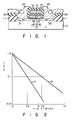
- Fig. 2 a graph illustrating data erase characteristics of the prior memory cell and the memory cell of Fig. 1.
- curve "a” indicates the data erase characteristic of the Fig. 1 memory cell in which the uppermost layer of the three-layered gate insulating layer is 15 ⁇ in thickness.
- Curve “b” indicates the data erase characteristic of the prior memory cell in which the uppermost layer of the three-layered gate insulating layer is 60 ⁇ .
- the data erase performance of the memory cell is generally described in term of the data erase time.
- the data erase time T (min.) is expressed by the time it takes the residual charges S in the floating gate to decrease from 100 per cent (full charge in the floating gate) to 10 per cent.
- the erase time Ta of the Fig. 1 memory cell is almost half the Tb of the prior memory cell.
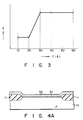
- Fig. 3 shows a relationship of the thickness "t" ( ⁇ ) of the silicon oxide layer 16 of the three-layered gate insulating layer 17 vs. data erase time T. As shown, the erase time T is almost constant over the thickness range from 10 to 20 ⁇ . It steeply increases when the thickness is 20 to 30 ⁇ , and reaches a peak at 30 ⁇ which is maintained for the thickness of more than 30 ⁇ . The Fig. 3 curve indicates that if the thickness of the top oxide silicon layer is 30 ⁇ or less, particularly 20 ⁇ or less, the erase time may be remarkably reduced.
- the third or top layer 16 is selected to be 10 ⁇ in thickness, the breakdown voltage is reduced. Therefore, the selection of such a figure for the the top layer thickness should be avoided.
- FIG. 1 A method of manufacturing the memory cell of Fig. 1 will be described referring to Figs. 4A to 4D.
- field insulating layer 11 is formed on the surface of substrate 10 made of P type silicon by a selective oxidization process. Then, the structure is thermally oxidized, thereby to form silicon oxide layer 31 of about 200 ⁇ thick on the surface of the element region on substrate 10. Polysilicon layer 32 of 4000 ⁇ is deposited over the entire surface of the resultant structure. Then, the phosphorus is doped into polysilicon layer 32, with the diffusion source of POCl3. (Fig. 4A).
- the surface of polysilicon layer 32 is oxidized by a dilution oxide process at 1000°C, to form silicon oxide layer 14 of 150 ⁇ , for example, on the surface of polysilicon layer 32.
- the silicon nitride layer 15 which is 150 ⁇ thick, for example, is deposited thereover by LP-CVD process.
- the structure thus formed is placed in a dry oxide atmosphere so that silicon oxide layer 16 is about 15 ⁇ thick is formed over the surface of silicon nitride layer 15. (Fig. 4B).
- polysilicon layer 33 of a 4000 ⁇ thickness is deposited over the entire surface of silicon oxide layer 16, and phosphorus is diffused from the diffusion source of POCl3 into polysilicon layer 33. (Fig. 4C).
- polysilicon layer 33, silicon oxide layer 16 layered thereunder, silicon nitride layer 15, oxide silicon layer 14, polysilicon layer 32 and silicon oxide layer 31 are selectively etched through a photo engraving process in a successive manner.
- floating gate 13 is formed above substrate 10, with gate insulating layer 12 interlayered between them.
- Floating gate 13 is the etched polysilicon layer 32.
- Gate insulating layer 12 is the etched silicon oxide layer 31.
- Gate insulating layer 17 of the three-layered structure is layered over floating gate 13. This is made up of silicon oxide layer 14, silicon nitride layer 15 and silicon oxide layer 16.
- arsenic ions are selectively implanted into the surface region of substrate 10, and the implanted ions are activated to form N+ type source region 21 and N+ type drain region 22. (Fig. 4D).
- the structure is placed in a dry oxide atmosphere, to form silicon oxide layer 19 (Fig. 1). Silicon oxide doped with phosphorus is deposited over the structure by CVD process, to form passivation layer 20 which is 0.8 ⁇ m thick thereover.
- the passivation layer 20 is photoetched to form contact holes 23 and 24.
- an aluminum-silicon alloy layer of 1.0 ⁇ m thickness is deposited over the entire surface of the structure, and patterned to form source lead electrode layer 25 and drain lead electrode layer 26.
- the nonvolatile semiconductor device of the ultraviolet erasable type as shown in Fig. 1 is completed.
- the present invention is not limited to the specific embodiment as mentioned above, but it may be changed and modified within the spirit and scope of the present invention.
- the polysilicon layer 32 forming floating gate 13 is set at a 4000 ⁇ thickness, and is doped with phosphorus. If necessary, phosphorus may be substituted with arsenic or borron. This layer 32 may be set at another proper thickness. Further, the LP-CVD process for the deposition of silicon nitride layer 15 may be substituted by direct nitride process or a plasma nitride process.
- the top silicon oxide layer 16 of the gate insulating layer 17 of the three-layered structure was formed by thermally processing the surface of nitride silicon layer 15 as the substrate for the top silicon oxide layer for about 80 minutes in a dry oxide atmosphere at 950°C. Any process may be used for forming the top silicon oxide layer 16, if it can form the silicon oxide layer of a 30 ⁇ thickness or less.
- control gate 18, which was the polysilicon layer in the above-mentioned embodiment, may consist of a high melting point polycide layer of the double layered structure, which is made up of a high melting point metal silicide layer and a polysilicon layer.
Abstract
Description
- This invention relates to an ultraviolet erasable nonvolatile semiconductor device having a floating gate and a control gate, in which the stored data is erasable by irradiation of ultraviolet rays.
- There is known an ultraviolet erasable nonvolatile semiconductor device having a floating gate, a control gate, and an insulating layer interlayered between these gates. This type of the memory device often employs a three-layered insulating layer for that gate insulating layer interlayered between the floating gate and the control gate. The three-layered gate insulating layer consists of a silicon oxide layer, a silicon nitride layer, and silicon oxide layer. Use of the gate insulating layer of the three-layered structure improves a breakdown voltage between the floating gate and the control gate, and additionally improves a defect density of the insulating layer per se. The oxide silicon layer as the top layer of the three-layered insulating layer is usually formed by oxidizing the silicon nitride layer by burning oxidization process. When an EPROM using memory cells whose gate insulating layer laid between the floating gate and the control gate utlized a three-layered structure, is compared with that using the memory cells whose gate insulating layer consists of only a silicon oxide layer, the former is inferior to the latter in the data erase characteristic. For details of this, reference is made to "Reliable CVD Interpoly Dielectrics for Advanced E and E²PROM" in technical digest paper,
page 16, in 1985 VLSI symposium. This paper describes that when the memory cell whose interlayered insulating layer utlizes a three-layered structure needs a long data erase time, approximately three times the data erase time of the memory cell whose interlayered insulating layer is a single silicon oxide layer formed by normal thermal oxidization process. - Accordingly, an object of this invention is to provide an ultraviolet erasable semiconductor device which may reduce the data erase time, while keeping high insulation and a low defect density. These are the advantages of the three-layered insulating layer which consistes of a silicon oxide layer, a silicon nitride layer and a silicon oxide layer.
- According to this invention, there is provided an ultraviolet erasable semiconductor device improved in that an insulating layer interlayered between the floating gate and the control gate which consists of three layers, a first silicon oxide layer, a silicon nitride layer layered on the first silicon oxide layer, and a second oxide layer layered on the silicon nitride layer, finally the second silicon oxide layer is the top layer of the three-layered insulating layer is 30 Å or less in thickness.
- This invention can be more fully understood from the following detailed description when taken in conjunction with the accompanying drawings, in which:
- Fig. 1 shows a sectional view of the structure of a memory cell, which is used in a ultraviolet erasable semiconductor device according to this invention;
- Fig. 2 graphically shows the relationship of a variation of the residual charge in a memory cell with respect to erase time;
- Fig. 3 graphically shows the relationship of a variation of erase time with respect to the thickness of the insulating layer of the memory cell; and
- Figs. 4A to 4D show sectional views listing a sequence of process steps to fabricate the memory cell.
- Reference is first made to Fig. 1 illustrating a cross section of one of the memory cells used in a ultra-violet erasable semiconductor device according to an embodiment of the present invention. As shown,
field insulating layer 11 as a silicon oxide layer (SiO₂) is formed on the surface ofsubstrate 10 made of P type silicon.Gate insulating layer 12 as a silicon oxide layer (SiO₂) of approximately 200 Å thick, is formed on a part of the surface ofsubstrate 10, which is isolated byfield insulating layer 11. Floatinggate 13 is formed ongate insulating layer 12. Floatinggate 13 is constructed with a polysilicon layer, which is doped with phosphorus, and is approximately 4000 Å in thickness.Gate insulating layer 17 of the three-layered structure is formed onfloating gate 13.Gate insulating layer 17 is made up of three layers. The first layer is a silicon oxide layer (SiO₂) of approximately 150 Å thick. The first layer is denoted as 14, constitutes the bottom layer of the three-layered structure ofgate insulating layer 17. The second layer is a silicon nitride layer (Si₃N₄) and is approximately 150 Å thick. The second layer is denoted as 15 and constitutes a medium layer of the three-layered structure. The third layer is a silicon oxide layer (SiO₂) of about 15 Å in thickness. The third layer is denoted as 16 and constitutes the top layer of the three-layered structure.Control gate 18 is formed over the three-layeredgate insulating layer 17.Control gate 18 is a polysilicon layer, which is doped with phosphorus, and is about 4000 Å in thickness. Source anddrain regions substrate 10. The layered structure made up ofgate insulating layer 12, floatinggate 13, three-layeredstructure insulating layer 17, andcontrol gate 18, is covered withsilicon oxide layer 19 and is approximately 400 Å thick. Thissilicon oxide layer 19 is covered further withpassivation layer 20.Passivation layer 20 is further layered on the surface offield insulating layer 11.Passivation layer 20 is made of silicon oxide and is approximately 0.8 µm thick. - Contact
holes lead electrode layer 25 and drainlead electrode layer 26 are formed in contact withsource region 21 anddrain region 22, throughcontact holes Electrode layers - As described above, in the memory cell structured as mentioned above, the
gate insulating layer 17 interlayered betweenfloating gate 13 andcontrol gate 18 is made up ofsilicon oxide layer 14 as a first layer, silicon nitride layer as a second layer, andoxide layer 16 as a third layer. The thickness of thethird layer 16, or the top layer of the three-layered structure is 15 Å, which is below 30 Å. - For writing data into the memory cell thus structured, a high voltage is applied to control
gate 18 anddrain region 22. At this time, 0 V, for example, is applied tosource region 21. When such voltages are applied to the memory cell, impact ionization causes a number of electron-hole pairs to be generated in the vicinity of the drain in the channel region between the source and drain. Of those electron-hole pairs, electrons are injected into floatinggate 13 and stored here. - For erasing the data thus stored in the memory cell, the memory cell is externally irradiated with ultraviolet rays. As the result of irradiation of ultraviolet rays, the electrons stored in floating
gate 13 are excited, and are discharged intocontrol gate 18 orsource region 21 anddrain region 22. Thus, the data is erased through the flow of the photocurrent. - As already mentioned, the thickness of the
uppermost layer 16 of thegate insulating layer 17 of the three-layered structure is 15 Å which is below 30 Å. Because of this small thickness figure, in an erasure mode, the photocurrent is easy to flow from floatinggate 13 to controlgate 18. When the memory cell whosegate insulating layer 17 is the three-layered gate insulating layer thus structured is compared with the memory cell whosegate insulating layer 17 is the three-layered structure with top silicon oxide layer more than of 30 Å as formed by ordinary burning oxidization process, a data erase time of the former is shorter than the latter. - Turning now to Fig. 2, a graph illustrating data erase characteristics of the prior memory cell and the memory cell of Fig. 1. In the graph, curve "a" indicates the data erase characteristic of the Fig. 1 memory cell in which the uppermost layer of the three-layered gate insulating layer is 15 Å in thickness. Curve "b" indicates the data erase characteristic of the prior memory cell in which the uppermost layer of the three-layered gate insulating layer is 60 Å. The data erase performance of the memory cell is generally described in term of the data erase time. As shown in Fig. 2, the data erase time T (min.) is expressed by the time it takes the residual charges S in the floating gate to decrease from 100 per cent (full charge in the floating gate) to 10 per cent. As seen from Fig. 2, the erase time Ta of the Fig. 1 memory cell is almost half the Tb of the prior memory cell. Fig. 3 shows a relationship of the thickness "t" (Å) of the
silicon oxide layer 16 of the three-layeredgate insulating layer 17 vs. data erase time T. As shown, the erase time T is almost constant over the thickness range from 10 to 20 Å. It steeply increases when the thickness is 20 to 30 Å, and reaches a peak at 30 Å which is maintained for the thickness of more than 30 Å. The Fig. 3 curve indicates that if the thickness of the top oxide silicon layer is 30 Å or less, particularly 20 Å or less, the erase time may be remarkably reduced. - In the three-layered
gate insulating layer 17, when the first orbottom layer 14 is about 150 Å thick, and the second ormedium layer 15 is about 150 Å, if the third ortop layer 16 is selected to be 10 Å in thickness, the breakdown voltage is reduced. Therefore, the selection of such a figure for the the top layer thickness should be avoided. - A method of manufacturing the memory cell of Fig. 1 will be described referring to Figs. 4A to 4D.
- To begin with,
field insulating layer 11 is formed on the surface ofsubstrate 10 made of P type silicon by a selective oxidization process. Then, the structure is thermally oxidized, thereby to formsilicon oxide layer 31 of about 200 Å thick on the surface of the element region onsubstrate 10.Polysilicon layer 32 of 4000 Å is deposited over the entire surface of the resultant structure. Then, the phosphorus is doped intopolysilicon layer 32, with the diffusion source of POCl₃. (Fig. 4A). - The surface of
polysilicon layer 32 is oxidized by a dilution oxide process at 1000°C, to formsilicon oxide layer 14 of 150 Å, for example, on the surface ofpolysilicon layer 32. Subsequently, thesilicon nitride layer 15 which is 150 Å thick, for example, is deposited thereover by LP-CVD process. The structure thus formed is placed in a dry oxide atmosphere so thatsilicon oxide layer 16 is about 15 Å thick is formed over the surface ofsilicon nitride layer 15. (Fig. 4B). - Following the above process step,
polysilicon layer 33 of a 4000 Å thickness is deposited over the entire surface ofsilicon oxide layer 16, and phosphorus is diffused from the diffusion source of POCl₃ intopolysilicon layer 33. (Fig. 4C). - Subsequently,
polysilicon layer 33,silicon oxide layer 16 layered thereunder,silicon nitride layer 15,oxide silicon layer 14,polysilicon layer 32 andsilicon oxide layer 31 are selectively etched through a photo engraving process in a successive manner. As a result, floatinggate 13 is formed abovesubstrate 10, withgate insulating layer 12 interlayered between them. Floatinggate 13 is the etchedpolysilicon layer 32.Gate insulating layer 12 is the etchedsilicon oxide layer 31.Gate insulating layer 17 of the three-layered structure is layered over floatinggate 13. This is made up ofsilicon oxide layer 14,silicon nitride layer 15 andsilicon oxide layer 16.Control gate 18, which is originally thepolysilicon layer 33, is layered overgate insulating layer 17. In the next step, arsenic ions are selectively implanted into the surface region ofsubstrate 10, and the implanted ions are activated to form N⁺type source region 21 and N⁺type drain region 22. (Fig. 4D). - The structure is placed in a dry oxide atmosphere, to form silicon oxide layer 19 (Fig. 1). Silicon oxide doped with phosphorus is deposited over the structure by CVD process, to form
passivation layer 20 which is 0.8 µm thick thereover. Thepassivation layer 20 is photoetched to form contact holes 23 and 24. Following this, an aluminum-silicon alloy layer of 1.0 µm thickness is deposited over the entire surface of the structure, and patterned to form sourcelead electrode layer 25 and drainlead electrode layer 26. At this point, the nonvolatile semiconductor device of the ultraviolet erasable type as shown in Fig. 1 is completed. - It should be understood that the present invention is not limited to the specific embodiment as mentioned above, but it may be changed and modified within the spirit and scope of the present invention. In the above-mentioned embodiment, the
polysilicon layer 32 forming floatinggate 13 is set at a 4000 Å thickness, and is doped with phosphorus. If necessary, phosphorus may be substituted with arsenic or borron. Thislayer 32 may be set at another proper thickness. Further, the LP-CVD process for the deposition ofsilicon nitride layer 15 may be substituted by direct nitride process or a plasma nitride process. In the above-mentioned embodiment, the topsilicon oxide layer 16 of thegate insulating layer 17 of the three-layered structure was formed by thermally processing the surface ofnitride silicon layer 15 as the substrate for the top silicon oxide layer for about 80 minutes in a dry oxide atmosphere at 950°C. Any process may be used for forming the topsilicon oxide layer 16, if it can form the silicon oxide layer of a 30 Å thickness or less. - Additionally,
control gate 18, which was the polysilicon layer in the above-mentioned embodiment, may consist of a high melting point polycide layer of the double layered structure, which is made up of a high melting point metal silicide layer and a polysilicon layer.
Claims (4)
Applications Claiming Priority (2)
| Application Number | Priority Date | Filing Date | Title |
|---|---|---|---|
| JP62190863A JP2633571B2 (en) | 1987-07-30 | 1987-07-30 | Ultraviolet erasing nonvolatile semiconductor device |
| JP190863/87 | 1987-07-30 |
Publications (2)
| Publication Number | Publication Date |
|---|---|
| EP0301460A2 true EP0301460A2 (en) | 1989-02-01 |
| EP0301460A3 EP0301460A3 (en) | 1990-01-10 |
Family
ID=16265021
Family Applications (1)
| Application Number | Title | Priority Date | Filing Date |
|---|---|---|---|
| EP88111965A Withdrawn EP0301460A3 (en) | 1987-07-30 | 1988-07-25 | Ultraviolet erasable nonvolatile semiconductor device |
Country Status (4)
| Country | Link |
|---|---|
| US (1) | US4943836A (en) |
| EP (1) | EP0301460A3 (en) |
| JP (1) | JP2633571B2 (en) |
| KR (1) | KR910007378B1 (en) |
Cited By (10)
| Publication number | Priority date | Publication date | Assignee | Title |
|---|---|---|---|---|
| FR2654259A1 (en) * | 1989-11-08 | 1991-05-10 | Samsung Electronics Co Ltd | SEMICONDUCTOR DEVICE COMPRISING A NITRIDE LAYER AND METHOD FOR MANUFACTURING SUCH A DEVICE. |
| EP0456319A2 (en) * | 1990-05-11 | 1991-11-13 | Koninklijke Philips Electronics N.V. | Floating gate field effect transistor structure and method for manufacturing the same |
| US5266509A (en) * | 1990-05-11 | 1993-11-30 | North American Philips Corporation | Fabrication method for a floating-gate field-effect transistor structure |
| DE19752434C2 (en) * | 1997-03-10 | 2000-10-19 | Mitsubishi Electric Corp | Non-volatile semiconductor memory device with a p-type doped floating gate electrode |
| US6509230B1 (en) | 1999-06-24 | 2003-01-21 | Lucent Technologies Inc. | Non-volatile memory semiconductor device including a graded, grown, high quality oxide layer and associated methods |
| US6521496B1 (en) * | 1999-06-24 | 2003-02-18 | Lucent Technologies Inc. | Non-volatile memory semiconductor device including a graded, grown, high quality control gate oxide layer and associated methods |
| US6551946B1 (en) | 1999-06-24 | 2003-04-22 | Agere Systems Inc. | Two-step oxidation process for oxidizing a silicon substrate wherein the first step is carried out at a temperature below the viscoelastic temperature of silicon dioxide and the second step is carried out at a temperature above the viscoelastic temperature |
| US6670242B1 (en) | 1999-06-24 | 2003-12-30 | Agere Systems Inc. | Method for making an integrated circuit device including a graded, grown, high quality gate oxide layer and a nitride layer |
| US7169714B2 (en) | 2000-01-11 | 2007-01-30 | Agere Systems, Inc. | Method and structure for graded gate oxides on vertical and non-planar surfaces |
| DE10302133B4 (en) * | 2002-01-21 | 2017-07-06 | Denso Corporation | A non-volatile semiconductor memory device having a floating gate surrounding conductive layer |
Families Citing this family (12)
| Publication number | Priority date | Publication date | Assignee | Title |
|---|---|---|---|---|
| US5104819A (en) * | 1989-08-07 | 1992-04-14 | Intel Corporation | Fabrication of interpoly dielctric for EPROM-related technologies |
| JP2602575B2 (en) * | 1990-07-06 | 1997-04-23 | シャープ株式会社 | Nonvolatile semiconductor memory device |
| JPH04144278A (en) * | 1990-10-05 | 1992-05-18 | Mitsubishi Electric Corp | Semiconductor storage device and manufacture thereof |
| KR100274555B1 (en) * | 1991-06-26 | 2000-12-15 | 윌리엄 비. 켐플러 | Insulated gate field effect transistor and manufacturing the same |
| US5495121A (en) * | 1991-09-30 | 1996-02-27 | Semiconductor Energy Laboratory Co., Ltd. | Semiconductor device |
| JPH05110114A (en) * | 1991-10-17 | 1993-04-30 | Rohm Co Ltd | Nonvolatile semiconductor memory device |
| US5619052A (en) * | 1994-09-29 | 1997-04-08 | Macronix International Co., Ltd. | Interpoly dielectric structure in EEPROM device |
| US6008091A (en) * | 1998-01-27 | 1999-12-28 | Lucent Technologies Inc. | Floating gate avalanche injection MOS transistors with high K dielectric control gates |
| US6969654B1 (en) * | 2000-06-19 | 2005-11-29 | Advanced Micro Devices, Inc. | Flash NVROM devices with UV charge immunity |
| US20030232507A1 (en) * | 2002-06-12 | 2003-12-18 | Macronix International Co., Ltd. | Method for fabricating a semiconductor device having an ONO film |
| CN100341139C (en) * | 2003-12-30 | 2007-10-03 | 旺宏电子股份有限公司 | Method for manufacturing nonvolatile memory element and metal interconnection wire preparing process |
| US7160775B2 (en) * | 2004-08-06 | 2007-01-09 | Freescale Semiconductor, Inc. | Method of discharging a semiconductor device |
Citations (2)
| Publication number | Priority date | Publication date | Assignee | Title |
|---|---|---|---|---|
| FR2533740A1 (en) * | 1982-09-24 | 1984-03-30 | Hitachi Ltd | REMANENT MEMORY |
| EP0187278A2 (en) * | 1984-12-07 | 1986-07-16 | Kabushiki Kaisha Toshiba | Semiconductor device and method for manufacturing the same |
Family Cites Families (4)
| Publication number | Priority date | Publication date | Assignee | Title |
|---|---|---|---|---|
| JPS577162A (en) * | 1980-06-17 | 1982-01-14 | Toshiba Corp | Nonvolatile semiconductor memory and manufacture therefor |
| US4577390A (en) * | 1983-02-23 | 1986-03-25 | Texas Instruments Incorporated | Fabrication of polysilicon to polysilicon capacitors with a composite dielectric layer |
| JPS60134478A (en) * | 1983-11-28 | 1985-07-17 | ローム・コーポレーション | Electrically programmalbe memory and method of producing same |
| US4665426A (en) * | 1985-02-01 | 1987-05-12 | Advanced Micro Devices, Inc. | EPROM with ultraviolet radiation transparent silicon nitride passivation layer |
-
1987
- 1987-07-30 JP JP62190863A patent/JP2633571B2/en not_active Expired - Fee Related
-
1988
- 1988-07-25 EP EP88111965A patent/EP0301460A3/en not_active Withdrawn
- 1988-07-25 US US07/224,026 patent/US4943836A/en not_active Expired - Lifetime
- 1988-07-30 KR KR1019880009746A patent/KR910007378B1/en not_active IP Right Cessation
Patent Citations (2)
| Publication number | Priority date | Publication date | Assignee | Title |
|---|---|---|---|---|
| FR2533740A1 (en) * | 1982-09-24 | 1984-03-30 | Hitachi Ltd | REMANENT MEMORY |
| EP0187278A2 (en) * | 1984-12-07 | 1986-07-16 | Kabushiki Kaisha Toshiba | Semiconductor device and method for manufacturing the same |
Cited By (11)
| Publication number | Priority date | Publication date | Assignee | Title |
|---|---|---|---|---|
| FR2654259A1 (en) * | 1989-11-08 | 1991-05-10 | Samsung Electronics Co Ltd | SEMICONDUCTOR DEVICE COMPRISING A NITRIDE LAYER AND METHOD FOR MANUFACTURING SUCH A DEVICE. |
| EP0456319A2 (en) * | 1990-05-11 | 1991-11-13 | Koninklijke Philips Electronics N.V. | Floating gate field effect transistor structure and method for manufacturing the same |
| EP0456319A3 (en) * | 1990-05-11 | 1991-12-18 | Koninklijke Philips Electronics N.V. | Floating gate field effect transistor structure and method for manufacturing the same |
| US5266509A (en) * | 1990-05-11 | 1993-11-30 | North American Philips Corporation | Fabrication method for a floating-gate field-effect transistor structure |
| DE19752434C2 (en) * | 1997-03-10 | 2000-10-19 | Mitsubishi Electric Corp | Non-volatile semiconductor memory device with a p-type doped floating gate electrode |
| US6509230B1 (en) | 1999-06-24 | 2003-01-21 | Lucent Technologies Inc. | Non-volatile memory semiconductor device including a graded, grown, high quality oxide layer and associated methods |
| US6521496B1 (en) * | 1999-06-24 | 2003-02-18 | Lucent Technologies Inc. | Non-volatile memory semiconductor device including a graded, grown, high quality control gate oxide layer and associated methods |
| US6551946B1 (en) | 1999-06-24 | 2003-04-22 | Agere Systems Inc. | Two-step oxidation process for oxidizing a silicon substrate wherein the first step is carried out at a temperature below the viscoelastic temperature of silicon dioxide and the second step is carried out at a temperature above the viscoelastic temperature |
| US6670242B1 (en) | 1999-06-24 | 2003-12-30 | Agere Systems Inc. | Method for making an integrated circuit device including a graded, grown, high quality gate oxide layer and a nitride layer |
| US7169714B2 (en) | 2000-01-11 | 2007-01-30 | Agere Systems, Inc. | Method and structure for graded gate oxides on vertical and non-planar surfaces |
| DE10302133B4 (en) * | 2002-01-21 | 2017-07-06 | Denso Corporation | A non-volatile semiconductor memory device having a floating gate surrounding conductive layer |
Also Published As
| Publication number | Publication date |
|---|---|
| KR910007378B1 (en) | 1991-09-25 |
| JPS6435964A (en) | 1989-02-07 |
| EP0301460A3 (en) | 1990-01-10 |
| JP2633571B2 (en) | 1997-07-23 |
| KR890003037A (en) | 1989-04-12 |
| US4943836A (en) | 1990-07-24 |
Similar Documents
| Publication | Publication Date | Title |
|---|---|---|
| EP0301460A2 (en) | Ultraviolet erasable nonvolatile semiconductor device | |
| KR100810710B1 (en) | Simultaneous formation of charge storage and bitline to worldline isolation | |
| US5656527A (en) | Method for fabricating a non-volatile semiconductor memory device having storage cell array and peripheral circuit, and a structure therefore | |
| US6723625B2 (en) | Semiconductor device having thin electrode laye adjacent gate insulator and method of manufacture | |
| EP1247299B1 (en) | Encapsulated tungsten gate mos transistor and memory cell and method of making same | |
| US6200858B1 (en) | Floating gate sidewall structure for the suppression of bird's beak | |
| US6358796B1 (en) | Method to fabricate a non-smiling effect structure in split-gate flash with self-aligned isolation | |
| EP0780902A1 (en) | Nonvolatile semiconductor memory and method for fabricating the same | |
| US5960283A (en) | Nonvolatile semiconductor memory device and method of fabrication of the same | |
| KR0138312B1 (en) | Manufacturing method of non-volatile semiconductor memory device | |
| US6326660B1 (en) | Method to improve the capacity of data retention and increase the coupling ratio of source to floating gate in split-gate flash | |
| JP3630491B2 (en) | Semiconductor device | |
| US7141850B2 (en) | Gated semiconductor assemblies and methods of forming gated semiconductor assemblies | |
| JP2855509B2 (en) | Method of manufacturing nonvolatile semiconductor memory device | |
| US5592002A (en) | Non-volatile semiconductor memory device having reduced current consumption | |
| US6268247B1 (en) | Memory cell of the EEPROM type having its threshold set by implantation, and fabrication method | |
| US6437424B1 (en) | Non-volatile semiconductor memory device with barrier and insulating films | |
| JPH05267684A (en) | Nonvolatile storage element | |
| US5565371A (en) | Method of making EPROM with separate erasing and programming regions | |
| JP3732649B2 (en) | Nonvolatile semiconductor memory device | |
| US7026685B2 (en) | Semiconductor devices having a non-volatile memory transistor and methods for manufacturing the same | |
| US5252846A (en) | Semiconductor memory device with an improved erroneous write characteristic and erasure characteristic | |
| EP0590319B1 (en) | A non-volatile memory cell | |
| EP0282023B1 (en) | Semiconductor memory device | |
| JP3388121B2 (en) | Nonvolatile semiconductor memory device, manufacturing method and charge storage method |
Legal Events
| Date | Code | Title | Description |
|---|---|---|---|
| PUAI | Public reference made under article 153(3) epc to a published international application that has entered the european phase |
Free format text: ORIGINAL CODE: 0009012 |
|
| 17P | Request for examination filed |
Effective date: 19880822 |
|
| AK | Designated contracting states |
Kind code of ref document: A2 Designated state(s): DE FR GB |
|
| PUAL | Search report despatched |
Free format text: ORIGINAL CODE: 0009013 |
|
| AK | Designated contracting states |
Kind code of ref document: A3 Designated state(s): DE FR GB |
|
| 17Q | First examination report despatched |
Effective date: 19910528 |
|
| STAA | Information on the status of an ep patent application or granted ep patent |
Free format text: STATUS: THE APPLICATION IS DEEMED TO BE WITHDRAWN |
|
| 18D | Application deemed to be withdrawn |
Effective date: 19920528 |