EP0303341A2 - Output buffer circuits - Google Patents
Output buffer circuits Download PDFInfo
- Publication number
- EP0303341A2 EP0303341A2 EP88305438A EP88305438A EP0303341A2 EP 0303341 A2 EP0303341 A2 EP 0303341A2 EP 88305438 A EP88305438 A EP 88305438A EP 88305438 A EP88305438 A EP 88305438A EP 0303341 A2 EP0303341 A2 EP 0303341A2
- Authority
- EP
- European Patent Office
- Prior art keywords
- output
- pull
- transistor
- coupled
- gate
- Prior art date
- Legal status (The legal status is an assumption and is not a legal conclusion. Google has not performed a legal analysis and makes no representation as to the accuracy of the status listed.)
- Granted
Links
Images


Classifications
-
- H—ELECTRICITY
- H03—ELECTRONIC CIRCUITRY
- H03K—PULSE TECHNIQUE
- H03K19/00—Logic circuits, i.e. having at least two inputs acting on one output; Inverting circuits
- H03K19/003—Modifications for increasing the reliability for protection
- H03K19/00346—Modifications for eliminating interference or parasitic voltages or currents
- H03K19/00361—Modifications for eliminating interference or parasitic voltages or currents in field effect transistor circuits
Definitions
- This invention relates generally to integrated circuits and more particularly, it relates to output buffer circuits which may be used, for example, for reducing significantly ground bounce noise.
- output buffer circuit is an important component for this interface function.
- the output buffer provides, when enabled, an output signal which is a function of data signal received from other logic circuitry of the integrated circuit.
- Output buffer circuits typically use a pull-up field-effect transistor (FET) and a pull-down field-effect transistor connected to an output terminal. Depending upon the state of the input data signal and an enable signal, either the pull-up or pull-down field-effect transistor is quickly turned on and the other one of them is turned off.
- FET field-effect transistor
- the output buffer circuits of the prior art have not been capable of providing output drive current of the magnitude possible with bipolar integrated circuits.
- the output buffer circuits to be described include a first pull-down transistor having a size equal to the size of the pull-up transistor and a second pull-down transistor having a larger size to accommodate the high current drive capability.
- the reduction in the bounce noise is achieved by delaying the turn-on of the second larger pull-down transistor until after the output has reached the low or logic "0" level.
- an improved output buffer which includes a first pull-down transistor having a size equal to the size of the pull-up transistor and a second pull-down transistor having a larger size to accommodate the high current drive capability.
- an improved output buffer which includes a first pull-down transistor, a second pull-down transistor, and a logic gate device for delaying the turn-on of the second pull-down transistor until after the output has reached the low logic level.
- an improved output buffer for producing an output signal at an output node which has a significant reduction in ground bounce noise which includes a pull-up transistor circuit, a pull-down transistor circuit, a first logic circuit, a second logic circuit, and a third logic circuit.
- the pull-up transistor circuit is responsive to a first control signal for generating slowly a transition from a low logic level to a high logic level at the output node.
- the pull-down transistor circuit is responsive to second and third control signals for generating slowly a transition from the high logic level to the low logic level at the output node.
- the pull-up circuit includes a pull-up transistor having one of its main electrodes coupled to a first power supply terminal, its other main electrode coupled to the output node, and its control electrode coupled to receive the first control signal.
- the pull-down circuit includes a first pull-down transistor having one of its main electrodes coupled to a second power supply terminal, its other main electrode coupled to the output node, and its control electrode coupled to receive the second control signal.
- the pull-down circuit further includes a second pull-down transistor having one of its main electrodes coupled to the second power supply terminal, its other main electrode coupled to the output node, and its control electrode coupled to receive the third control signal.
- the first logic circuit is responsive to a data input signal making a low-to-high transition and the output signal making a low-to-high transition for generating the first control signal.
- the second logic circuit is responsive to the data input signal making a high-to-low transition and the output signal making a high-to-low transition for generating the second control signal.
- the third logic circuit is responsive to the data input signal making the high-to-low transition and the output signal making the high-to-low transition for maintaining the second pull-down transistor turned-off until after the output node has made the high-to-low transition, thereby reducing significantly the ground bounce noise.
- FIG. 1 a schematic circuit diagram of a prior art output buffer circuit 10 formed of an N-channel pull-up field-effect transistor (FET) N1 and an N-channel pull-down FET N2.
- the buffer circuit 10 provides an output signal at an output node A in response to a data input signal D received at data input node B and an enable signal OE received at enable input node C.
- the buffer circuit 10 includes NOR logic gates 12, 14 and inverters 16, 18, 20, 22. Power for all of the components of the buffer circuit 10 is provided by first external and second external power supply terminals 24, 26.
- a first supply potential VCC is supplied at the first terminal 24, and a second supply or ground potential GND is applied at the second terminal 26.
- the output node A of the buffer circuit 10 is used to drive a capacitive load formed of a resistance R L and a capacitor C L .
- the first external power supply terminal 24 is connected to an internal supply potential node D via a series-connected resistor R1 and inductor L1 which represent the impedance and inductance components in the power supply line.
- the second external power supply terminal 26 is connected to an internal ground potential node E via a series-connected resistor R2 and inductor L2 which represent the impedance and inductance components in the power supply line.
- the NOR gate 12 receives the enable signal OE on line 28, the inverted or complement of the data input signal D on line 30, and the complement of the data input signal D on line 32.
- the data input signal D is inverted three times via the inverters 16, 18 and 20 to produce the inverted data input signal D on the line 30.
- the data input signal D is also inverted once by the inverter 16 to produce the inverted data input signal D on the line 32.
- the output of the NOR gate 12 is supplied to the gate of the pull-up transistor N1.
- the NOR gate 14 receives the same enable signal OE on line 34, the non-inverted data input signal D on line 36, the non-inverted data input signal on line 38.
- the data input signal D is inverted two times via the inverters 16 and 22 to produce the non-inverted data input signal D on the line 36.
- the data input signal D received at the node B is also fed directly via the line 38 to the input of the NOR gate 14.
- the output of the NOR gate 14 is supplied to the gate of the pull-down transistor N2.
- the physical size of the pull-down transistor N2 is made to be approximately twice the size of the pull-up transistor N1.
- the turning-on of the transistor N2 will generate a large instantaneous current flowing into the inductive L2 which will cause voltage variations producing ground bounce noise at the internal ground potential node E.
- the turning-on of the transistor N1 will generate a similar instantaneous current flowing into the inductive L1 which will cause voltage variations producing output signal ringing at the internal supply potential node D.
- the fluctuation at the node D will be smaller than the ones at the node E. Therefore, it can be seen that the high drive current can be achieved with the output buffer circuit 10 only at the expense of sacrificing speed and an increase in output signal distortion due to internal ground bounce noise and/or output signal ringing.
- FIG 2 there is shown an output buffer circuit 10a of the present invention which represents an improvement over the buffer circuit 10 of Figure 1.
- the output buffer circuit 10a provides a high current drive capability comparable to the bipolar I.C. but yet reduces significantly the distortion in the output signal due to ground bounce noise.
- the output buffer circuit 10a provides an output signal at an output node A in response to a data input signal D received at data input node B and a first enable signal OE received at enable input node C and a second enable signal OE received at enable input node F.
- the output buffer circuit 10a includes NOR logic gates 12, 13, 14, 15; inverters 16, 18, 20, 22; AND logic gate 17; enable transistors N4, N6; control transistors N5, N7; a pull-up transistor N1; and first and second pull-down transistors N3, N8.
- the power for the buffer circuit 10a is provided by first external and second external power supply terminals 24 and 26.
- a first power supply potential VCC is applied at the first terminal 24 and a second supply or ground potential GND is applied at the second terminal 26.
- the NOR gate 12 receives the enable signal OE on line 28, the inverted or complement of the data input signal D on line 30, and the complement of the data input signal D on line 32.
- the data input signal D is inverted three times via the inverters 16, 18 and 20 to produce the inverted data input signal D on the line 30.
- the data input signal D is also inverted once by the inverter 16 to produce the inverted data input signal D on the line 32.
- the output of the NOR gate 12 is supplied to the gate of the pull-up transistor N1 at node 3.
- the NOR gate 14 receives the same enable signal OE on line 34, the non-inverted data input signal D on line 36, and the non-inverted data input signal D on line 38.
- the data input signal D is inverted two times via the inverters 16 and 22 to produce the non-inverted data input signal D on the line 36.
- the data input signal D received at the node B is also fed directly via the line 38 to the input of the NOR gate 14.
- the output of the NOR gate 14 is supplied to the gate of the first pull-down transistor N3 at node 4.
- the NOR gate 13 receives the inverted data input signal D via the output of the inverter 16 on line 40 and receives the output signal at the output node A on line 42.
- the output of the NOR gate 13 is supplied to the gate of the control transistor N5 at node 6.
- the transistor N5 has its drain connected to the source of the enable transistor N4 and its source also connected to the node 3.
- the enable transistor N4 has its gate connected to the enable signal OE at the node F and its drain connected to the drain of the pull-up transistor N1.
- the AND gate 17 receives the output signal at the output node A on line 44 and receives the inverted data signal D on line 46.
- the output of the AND gate 17 is applied to the gate of the control transistor N7 at node 7.
- the transistor N7 has its drain connected to the source of the enable transistor N6 and its source connected to the node 4.
- the transistor N6 has its drain connected to the drains of the pull-up transistors N3, N8 or output node A and its gate connected to the second enable signal OE.
- the NOR gate 15 receives the first enable signal OE on line 48, the output signal at the output node A on line 50, and the data input signal D on line 52.
- the output of the NOR gate 15 is supplied to the gate of the second pull-down transistor N8.
- the transistors N3 and N8 have their drain-source conduction paths connected in parallel between the output node A and the internal ground node E. Specifically, the drains of the transistors N3 and N8 are connected to the output node A and the sources thereof are connected to the node E.
- Figures 3(a)-3(h) of the drawings illustrate the waveforms appearing at various points in the output buffer circuit 10a of Figure 2 so as to provide an understanding of the operation of the present invention.
- the pull-up action of Figure 2 will now be explained. Initially, it will be assumed that the first enable signal OE is low, the second enable signal OE is high, and the output signal at the output node A is low at the time t0 ⁇ .
- the waveform of the output node A is shown in Figure 3(c).
- the enable transistors N4 and N6 are both turned on. Further, it will be assumed that the first and second pull-down transistors are both turned on.
- the output of the NOR gate 13 is switched from a low level to a high level at the time t2 as shown in Figure 3(g).
- This will cause the control transistor N5 to turn on and thus the node 3 will begin to rise toward the supply potential VCC via the transistors N4 and N5 as depicted in Figure 3(d).
- the node 3 will only reach the voltage determined by the ratio of the turn-on resistors in the transistors N4 and N5 and the NOR gate 12 since the output of the NOR gate 12 is initially low. This voltage at the node 3 will be below the supply potential VCC. This is shown at point X in Figure 3(d).
- the node 3 will eventually reach the supply potential VCC after the output of the NOR gate 12 has switched from the low level to the high level. As can be seen from Figure 3(g), the output of the NOR gate 13 will be switched back to the low level at the time t3 after the output node A has gone high. Since the NOR gate 13 and the control transistor N5 are used to turn on slowly the pull-up transistor N1, this reduces the instantaneous pull-up current through the transistor N1 and thus minimizes the noise generated across the series-connected resistor R1 and the inductor L1 which are connected to the supply potential VCC.
- the node 4 will only reach the voltage determined by the ratio of the turn-on resistors in the transistors N6 and N7 and the NOR gate 14 since the NOR gate 14 is initially low. This voltage at the node 4 will be less than the high level voltage at the node A which is less than the supply potential VCC. This is shown at point Y in Figure 3(e). The node 4 will eventually reach the supply potential VCC after the output of the NOR gate 14 has switched from the low level to the high level. As a result, the output node A, as shown in Figure 3(c), will be pulled low at the time t8.
- the output of the AND gate 17 will be switched back to the low level at the time t9 after the output node A has gone low. Only after the output node A is low, the output of the NOR gate 15 at node 5 will start to rise, thereby causing the delayed turn-on of the second pull-down transistor N8.
- the instantaneous current through the transistor N3 will be smaller than the current through the transistor N2 of Figure 1.
- the size of the first pull-down transistor N3 will be made equal to the size of the pull-up transistor N1, and the size of the second pull-down transistor N8 will be of an equal or larger size than the first pull-down transistor N3 in order to provide the high drive capability.
- the second pull-down transistor N8 will not be turned on until after the output has reached a low level.
- the second pull-down transistor is delayed in its turn-on with respect to the turn-on of the first pull-down transistor N3 which reduces significantly the ground bounce noise due to the inductance in the power supply lines.
- FIG 4 there is shown a schematic circuit diagram of a prior art full CMOS output buffer circuit 110 formed of a P-channel pull-up field-effect transistor (FET) P1 and an N-channel pull-down FET N2.
- the buffer circuit 110 provides an output signal at an output node A in response to a data input signal D received at data input node B, a first enable signal OE received at enable input node C, and a second enable signal OE received at enable input node F. Since the circuit of Figure 4 is substantially identical to the circuit of Figure 1, only the differences will now be discussed.
- the NOR gate 12 in Figure 1 has been replaced by a NAND gate 12a. Further, the inverters 18 and 20 in Figure 1 have now been eliminated. Except for these changes, the operation of the circuit in Figure 4 is substantially identical to the circuit of Figure 1.
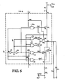
- FIG. 5 there is depicted a schematic circuit diagram of an alternate embodiment of an output buffer 110a constructed according to the present invention.
- the output buffer circuit 110a represents an improvement over the buffer circuit 110 of Figure 4.
- the output buffer circuit 110a provides a high current drive capability comparable to the bipolar I.C. but yet reduces significantly the distortion in the output signal due to ground bounce noise.
- the output buffer circuit 110a provides an output signal at an output node A in response to a data input signal D received at data input node B, a first enable signal OE received at enable input node C, and a second enable signal OE received at enable input node F.
- the circuit of Figure 5 is substantially identical to the circuit of Figure 2, except that the NOR gate 12 of Figure 2 has been replaced by a NAND gate 12b.
- the inverters 18 and 20 of Figure 1 have been eliminated, and the connection of the control transistors N4 and N6 have been modified.
- the size of the first pull-down transistor N3 is smaller in size than the pull-up transistor P1
- the size of the second pull-down transistor N8 is equal or larger in size than the first pull-down transistor N3.
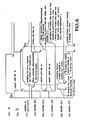
- FIG. 6(a) - 6(h) there are illustrated waveforms at various points in the circuit of Figure 5. As can be seen, these waveforms are substantially identical to the waveforms of Figure 3(a)-3(h) except for Figure 6(d). This is the waveform at the node 3 or at the gate of the P-channel pull-up transistor P1. As can be seen, this waveform is inverted from the waveform of Figure 3(d).
- the present invention provides improved output buffer circuits formed of a first pull-down transistor and a second pull-down transistor for reducing significantly ground bounce noise. This performance is achieved by delaying the turn-on of the second pull-down transistor until the output has reached the low level.
Abstract
Description
- This invention relates generally to integrated circuits and more particularly, it relates to output buffer circuits which may be used, for example, for reducing significantly ground bounce noise.
- As is well known, digital logic circuits are widely used in the electronics field. One such use is for the interfacing between the logic of one integrated circuit device and another integrated circuit device. An output buffer circuit is an important component for this interface function. The output buffer provides, when enabled, an output signal which is a function of data signal received from other logic circuitry of the integrated circuit.
- Output buffer circuits typically use a pull-up field-effect transistor (FET) and a pull-down field-effect transistor connected to an output terminal. Depending upon the state of the input data signal and an enable signal, either the pull-up or pull-down field-effect transistor is quickly turned on and the other one of them is turned off.
- In general, the output buffer circuits of the prior art have not been capable of providing output drive current of the magnitude possible with bipolar integrated circuits. There have been attempts made to achieve higher output drive currents from output buffers by increasing the size of the pull-down field-effect transistor to approximately twice the size of the pull-up field-effect transistor. However, this has resulted in sacrifices in speed and output signal distortion due to the large instantaneous current, when the pull-down transistor is turned on, flowing through the impedance and inductance components of the power supply lines to cause inductive noise at the internal ground potential node of the output buffer.
- It would therefore be desirable to provide improved output buffer circuits which have a high current drive capability comparable to the bipolar integrated circuits but yet reduces significantly the distortion in the output signal due to ground bounce noise. The output buffer circuits to be described include a first pull-down transistor having a size equal to the size of the pull-up transistor and a second pull-down transistor having a larger size to accommodate the high current drive capability. The reduction in the bounce noise is achieved by delaying the turn-on of the second larger pull-down transistor until after the output has reached the low or logic "0" level.
- We will describe improved output buffers which are relatively simple and economical to manufacture and assemble, but yet overcomes the disadvantages of the prior art output buffers.
- We will describe an improved output buffer which has a significant reduction in ground bounce noise.
- We will describe an improved output buffer which includes a first pull-down transistor having a size equal to the size of the pull-up transistor and a second pull-down transistor having a larger size to accommodate the high current drive capability.
- We will describe an improved output buffer which includes a first pull-down transistor, a second pull-down transistor, and a logic gate device for delaying the turn-on of the second pull-down transistor until after the output has reached the low logic level.
- In accordance with these aims and objectives, we will describe, in particular, an improved output buffer for producing an output signal at an output node which has a significant reduction in ground bounce noise which includes a pull-up transistor circuit, a pull-down transistor circuit, a first logic circuit, a second logic circuit, and a third logic circuit. The pull-up transistor circuit is responsive to a first control signal for generating slowly a transition from a low logic level to a high logic level at the output node. The pull-down transistor circuit is responsive to second and third control signals for generating slowly a transition from the high logic level to the low logic level at the output node. The pull-up circuit includes a pull-up transistor having one of its main electrodes coupled to a first power supply terminal, its other main electrode coupled to the output node, and its control electrode coupled to receive the first control signal. The pull-down circuit includes a first pull-down transistor having one of its main electrodes coupled to a second power supply terminal, its other main electrode coupled to the output node, and its control electrode coupled to receive the second control signal. The pull-down circuit further includes a second pull-down transistor having one of its main electrodes coupled to the second power supply terminal, its other main electrode coupled to the output node, and its control electrode coupled to receive the third control signal.
- The first logic circuit is responsive to a data input signal making a low-to-high transition and the output signal making a low-to-high transition for generating the first control signal. The second logic circuit is responsive to the data input signal making a high-to-low transition and the output signal making a high-to-low transition for generating the second control signal. The third logic circuit is responsive to the data input signal making the high-to-low transition and the output signal making the high-to-low transition for maintaining the second pull-down transistor turned-off until after the output node has made the high-to-low transition, thereby reducing significantly the ground bounce noise.
- These and other objects and advantages of the present invention will become more fully apparent from the following detailed description when read in conjunction with the accompanying drawings with like reference numerals indicating corresponding parts throughout, wherein
- Figure 1 is a schematic circuit diagram of a prior art output buffer circuit utilizing an N-channel pull-up FET and an N-channel pull-down FET;
- Figure 2 is a schematic circuit diagram of an output buffer circuit constructed in accordance with the principles of the present invention;
- Figures 3(a) - 3(h) are waveforms at various points in the circuit of Figure 2;
- Figure 4 is a schematic circuit diagram of a prior art CMOS output buffer circuit utilizing a P-channel pull-up FET and an N-channel pull-down FET;
- Figure 5 is a schematic diagram of a second embodiment of the output buffer circuit of the present invention; and
- Figures 6(a) - 6(h) are waveforms at various points in the circuit of Figure 4.
- Referring now to the drawings, there is shown in Figure 1 a schematic circuit diagram of a prior art
output buffer circuit 10 formed of an N-channel pull-up field-effect transistor (FET) N1 and an N-channel pull-down FET N2. Thebuffer circuit 10 provides an output signal at an output node A in response to a data input signal D received at data input node B and an enable signalOE received at enable input node C. Thebuffer circuit 10 includesNOR logic gates inverters buffer circuit 10 is provided by first external and second externalpower supply terminals first terminal 24, and a second supply or ground potential GND is applied at thesecond terminal 26. - The output node A of the
buffer circuit 10 is used to drive a capacitive load formed of a resistance RL and a capacitor CL. The first externalpower supply terminal 24 is connected to an internal supply potential node D via a series-connected resistor R1 and inductor L1 which represent the impedance and inductance components in the power supply line. Similarly, the second externalpower supply terminal 26 is connected to an internal ground potential node E via a series-connected resistor R2 and inductor L2 which represent the impedance and inductance components in the power supply line. - The
NOR gate 12 receives the enable signalOE online 28, the inverted or complement of the data input signal D online 30, and the complement of the data input signal D online 32. The data input signal D is inverted three times via theinverters D on theline 30. The data input signal D is also inverted once by theinverter 16 to produce the inverted data input signalD on theline 32. The output of theNOR gate 12 is supplied to the gate of the pull-up transistor N1. - The NOR
gate 14 receives the same enable signalOE online 34, the non-inverted data input signal D online 36, the non-inverted data input signal online 38. The data input signal D is inverted two times via theinverters line 36. The data input signal D received at the node B is also fed directly via theline 38 to the input of theNOR gate 14. The output of theNOR gate 14 is supplied to the gate of the pull-down transistor N2. - When the enable signal
OE is at a low or logic "0" level (GND) and the data input signal D is at a high (VCC) or logic "1" level, the output of theNOR gate 12 will be at the high level and the output of theNOR gate 14 will be at the low level. This causes a logic "1" (VCC) to be applied to the gate of the transistor N1 and a logic "0" (GND) to be applied to the gate of the transistor N2. As a result, the N-channel FET N1 is turned on and the N-channel FET N2 is turned off. Thus, the output node A is pulled up toward the supply potential VCC. - On the other hand, when the enable signal
OE is at a low or logic "0" level (GND) and the data input signal D is at a low (GND) or logic "0" level, the output of theNOR gate 12 will be at the low level and the output of theNOR gate 14 will be at the high level. This causes a logic "0" (GND) to be applied to the gate of the transistor N1 and a logic "1" (VCC) to be applied to the gate of the transistor N2. As a result, the output node A is pulled down toward the ground potential. - When the enable signal
OE is at the high or logic "1" level (VCC), the outputs of bothNOR gates output buffer circuit 10 is not enabled. - In order to increase the magnitude of the drive current in the
output buffer circuit 10 so as to be equal to the prior art bipolar output buffers, the physical size of the pull-down transistor N2 is made to be approximately twice the size of the pull-up transistor N1. As a consequence, the turning-on of the transistor N2 will generate a large instantaneous current flowing into the inductive L2 which will cause voltage variations producing ground bounce noise at the internal ground potential node E. Also, the turning-on of the transistor N1 will generate a similar instantaneous current flowing into the inductive L1 which will cause voltage variations producing output signal ringing at the internal supply potential node D. However, the fluctuation at the node D will be smaller than the ones at the node E. Therefore, it can be seen that the high drive current can be achieved with theoutput buffer circuit 10 only at the expense of sacrificing speed and an increase in output signal distortion due to internal ground bounce noise and/or output signal ringing. - In Figure 2, there is shown an output buffer circuit 10a of the present invention which represents an improvement over the
buffer circuit 10 of Figure 1. The output buffer circuit 10a provides a high current drive capability comparable to the bipolar I.C. but yet reduces significantly the distortion in the output signal due to ground bounce noise. The output buffer circuit 10a provides an output signal at an output node A in response to a data input signal D received at data input node B and a first enable signalOE received at enable input node C and a second enable signal OE received at enable input node F. - The output buffer circuit 10a includes
NOR logic gates inverters logic gate 17; enable transistors N4, N6; control transistors N5, N7; a pull-up transistor N1; and first and second pull-down transistors N3, N8. The power for the buffer circuit 10a is provided by first external and second externalpower supply terminals first terminal 24 and a second supply or ground potential GND is applied at thesecond terminal 26. - The NOR
gate 12 receives the enable signalOE online 28, the inverted or complement of the data input signal D online 30, and the complement of the data input signal D online 32. The data input signal D is inverted three times via theinverters D on theline 30. The data input signal D is also inverted once by theinverter 16 to produce the inverted data input signalD on theline 32. The output of the NORgate 12 is supplied to the gate of the pull-up transistor N1 atnode 3. - The NOR
gate 14 receives the same enable signalOE online 34, the non-inverted data input signal D online 36, and the non-inverted data input signal D online 38. The data input signal D is inverted two times via theinverters line 36. The data input signal D received at the node B is also fed directly via theline 38 to the input of the NORgate 14. The output of the NORgate 14 is supplied to the gate of the first pull-down transistor N3 atnode 4. - The NOR
gate 13 receives the inverted data input signalD via the output of theinverter 16 on line 40 and receives the output signal at the output node A online 42. The output of the NORgate 13 is supplied to the gate of the control transistor N5 atnode 6. The transistor N5 has its drain connected to the source of the enable transistor N4 and its source also connected to thenode 3. The enable transistor N4 has its gate connected to the enable signal OE at the node F and its drain connected to the drain of the pull-up transistor N1. - The AND
gate 17 receives the output signal at the output node A online 44 and receives the inverted data signalD on line 46. The output of the ANDgate 17 is applied to the gate of the control transistor N7 atnode 7. The transistor N7 has its drain connected to the source of the enable transistor N6 and its source connected to thenode 4. The transistor N6 has its drain connected to the drains of the pull-up transistors N3, N8 or output node A and its gate connected to the second enable signal OE. - The NOR
gate 15 receives the first enable signalOE online 48, the output signal at the output node A online 50, and the data input signal D online 52. The output of the NORgate 15 is supplied to the gate of the second pull-down transistor N8. The transistors N3 and N8 have their drain-source conduction paths connected in parallel between the output node A and the internal ground node E. Specifically, the drains of the transistors N3 and N8 are connected to the output node A and the sources thereof are connected to the node E. - Reference is now made to Figures 3(a)-3(h) of the drawings which illustrate the waveforms appearing at various points in the output buffer circuit 10a of Figure 2 so as to provide an understanding of the operation of the present invention. The pull-up action of Figure 2 will now be explained. Initially, it will be assumed that the first enable signal
OE is low, the second enable signal OE is high, and the output signal at the output node A is low at the time t0̸. The waveform of the output node A is shown in Figure 3(c). Thus, the enable transistors N4 and N6 are both turned on. Further, it will be assumed that the first and second pull-down transistors are both turned on. This is because at the time t0̸ the gates (nodes 4 and 5) of the respective transistors N3 and N8 are at the high level. The waveforms at thenodes D makes a high-to- low transition instantaneously (Figure 3(b)), the transistors N3 and N8 are quickly turned off as can be seen from Figures 3(e) and 3(f). However, the output signal at the node A (Figure 3(c)) still remains at the low level. - As a result, the output of the NOR
gate 13 is switched from a low level to a high level at the time t2 as shown in Figure 3(g). This will cause the control transistor N5 to turn on and thus thenode 3 will begin to rise toward the supply potential VCC via the transistors N4 and N5 as depicted in Figure 3(d). However, thenode 3 will only reach the voltage determined by the ratio of the turn-on resistors in the transistors N4 and N5 and the NORgate 12 since the output of the NORgate 12 is initially low. This voltage at thenode 3 will be below the supply potential VCC. This is shown at point X in Figure 3(d). Thenode 3 will eventually reach the supply potential VCC after the output of the NORgate 12 has switched from the low level to the high level. As can be seen from Figure 3(g), the output of the NORgate 13 will be switched back to the low level at the time t3 after the output node A has gone high. Since the NORgate 13 and the control transistor N5 are used to turn on slowly the pull-up transistor N1, this reduces the instantaneous pull-up current through the transistor N1 and thus minimizes the noise generated across the series-connected resistor R1 and the inductor L1 which are connected to the supply potential VCC. - The pull-down action of Figure 2 will now be described. This occurs at the time t5 when the inverted data signal
D makes a low-to-high transition as is illustrated in Figure 3(b). As a result, the pull-up transistor N1 will be quickly turned off at the time t6 as shown in Figure 3(d). Since the output node A will remain high at the time t5, as shown in Figure 3(c), this causes the output of the ANDgate 17 to switch from a low level to a high level at the time t7. This is depicted in Figure 3(h). As a consequence, the control transistor N7 is turned on and thus thenode 4 will begin to rise toward the supply potential VCC as depicted in Figure 3(e). However, thenode 4 will only reach the voltage determined by the ratio of the turn-on resistors in the transistors N6 and N7 and the NORgate 14 since the NORgate 14 is initially low. This voltage at thenode 4 will be less than the high level voltage at the node A which is less than the supply potential VCC. This is shown at point Y in Figure 3(e). Thenode 4 will eventually reach the supply potential VCC after the output of the NORgate 14 has switched from the low level to the high level. As a result, the output node A, as shown in Figure 3(c), will be pulled low at the time t8. As can be seen from Figure 3(h), the output of the ANDgate 17 will be switched back to the low level at the time t9 after the output node A has gone low. Only after the output node A is low, the output of the NORgate 15 atnode 5 will start to rise, thereby causing the delayed turn-on of the second pull-down transistor N8. - Since the AND
gate 17 and the control transistor N7 are used to turn on slowly the pull-down transistor N3 so as to start the pull-down action, the instantaneous current through the transistor N3 will be smaller than the current through the transistor N2 of Figure 1. This is achieved by also splitting the pull-down transistor N2 (Figure 1) into two transistors N3 and N8. The size of the first pull-down transistor N3 will be made equal to the size of the pull-up transistor N1, and the size of the second pull-down transistor N8 will be of an equal or larger size than the first pull-down transistor N3 in order to provide the high drive capability. It will be noted that the second pull-down transistor N8 will not be turned on until after the output has reached a low level. Thus, the second pull-down transistor is delayed in its turn-on with respect to the turn-on of the first pull-down transistor N3 which reduces significantly the ground bounce noise due to the inductance in the power supply lines. - In Figure 4, there is shown a schematic circuit diagram of a prior art full CMOS
output buffer circuit 110 formed of a P-channel pull-up field-effect transistor (FET) P1 and an N-channel pull-down FET N2. Thebuffer circuit 110 provides an output signal at an output node A in response to a data input signal D received at data input node B, a first enable signalOE received at enable input node C, and a second enable signal OE received at enable input node F. Since the circuit of Figure 4 is substantially identical to the circuit of Figure 1, only the differences will now be discussed. The NORgate 12 in Figure 1 has been replaced by aNAND gate 12a. Further, theinverters - Referring now to Figure 5, there is depicted a schematic circuit diagram of an alternate embodiment of an output buffer 110a constructed according to the present invention. The output buffer circuit 110a represents an improvement over the
buffer circuit 110 of Figure 4. The output buffer circuit 110a provides a high current drive capability comparable to the bipolar I.C. but yet reduces significantly the distortion in the output signal due to ground bounce noise. The output buffer circuit 110a provides an output signal at an output node A in response to a data input signal D received at data input node B, a first enable signalOE received at enable input node C, and a second enable signal OE received at enable input node F. The circuit of Figure 5 is substantially identical to the circuit of Figure 2, except that the NORgate 12 of Figure 2 has been replaced by aNAND gate 12b. Further, theinverters - Except for these changes, the operation of the circuit of Figure 5 is substantially identical to the circuit of Figure 2 and thus will not be generally repeated. In Figures 6(a) - 6(h), there are illustrated waveforms at various points in the circuit of Figure 5. As can be seen, these waveforms are substantially identical to the waveforms of Figure 3(a)-3(h) except for Figure 6(d). This is the waveform at the
node 3 or at the gate of the P-channel pull-up transistor P1. As can be seen, this waveform is inverted from the waveform of Figure 3(d). - While the output buffer circuits 10a and 110a of Figures 2 and 5 have been shown with enable transistors, it should be understood by those skilled in the art that these transistors could be eliminated if the high impedance tri-state mode of operation is now required. From the foregoing detailed description, it can thus be seen that the present invention provides improved output buffer circuits formed of a first pull-down transistor and a second pull-down transistor for reducing significantly ground bounce noise. This performance is achieved by delaying the turn-on of the second pull-down transistor until the output has reached the low level.
- While there has been illustrated and described what are at present considered to be preferred embodiments of the present invention, it will be understood by those skilled in the art that various changes and modifications may be made, and equivalents may be substituted for elements thereof without departing from the true scope of the invention. In addition, many modifications may be made to adapt a particular situation or material to the teachings of the invention without departing from the central scope thereof. Therefore, it is intended that this invention not be limited to the particular embodiments disclosed as the best modes contemplated for carrying out the invention, but that the invention will include all embodiments falling within the scope of the appended claims.
Claims (20)
pull-up circuit means responsive to a first control signal for generating slowly a transition from a low logic level to a high logic level at the output node;
said pull-up circuit means including a pull-up transistor having one of its main electrodes coupled to a first power supply terminal, its other main electrode coupled to the output node, and its control electrode coupled to receive the first control signal;
pull-down circuit means responsive to second and third control signals for generating slowly a transition from the high logic level to the low logic level at the output node;
said pull-down circuit means including a first pull-down transistor having one of its main electrodes coupled to a second power supply terminal, its other main electrode copled to the output node, and its control electrode coupled to receive the second control signal;
said pull-down circuit means further including a second pull-down transistor having one of its main electrodes coupled to the second power supply terminal, its other main electrode coupled to the output node, and its control electrode copled to receive the third control signal;
first logic means responsive to a data input signal making a low-to-high transition and the output signal making a low-to-high transition for generating the first control signal;
second logic means responsive to the data input signal making a high-to-low transition and the output signal making a high-to-low transition for generating the second control signal; and
third logic means responsive to the data input signal making the high-to-low transition and the output signal making the high-to-low transition for maintaining the second pull-down transistor turned-off until after the output node has made the high-to-low transition, thereby reducing significantly the ground bounce noise.
pull-up circuit means responsive to a first control signal for generating slowly a transition from a low logic level to a high logic level at the output node;
pull-down circuit means responsive to second and third control signals for generating slowly a transition from the high logic level to the low logic level at the output node;
first logic means responsive to a data input signal making a low-to-high transition and the output signal making a low-to-high transition for generating the first control signal;
second logic means responsive to the data input signal making a high-to-low transition and the output signal making a high-to-low transition for generating the second control signal; and
third logic means having first and second current paths respectively responsive to the data input signal making the high-to-low transition and the output signal making the high-to-low transition for generating the third control signal to maintain said second current path turned-off until after the output node has made the high-to-low transition, thereby reducing significantly the ground bounce noise.
Priority Applications (1)
| Application Number | Priority Date | Filing Date | Title |
|---|---|---|---|
| AT88305438T ATE93351T1 (en) | 1987-08-13 | 1988-06-15 | OUTPUT BUFFER CIRCUITS. |
Applications Claiming Priority (2)
| Application Number | Priority Date | Filing Date | Title |
|---|---|---|---|
| US07/085,104 US4777389A (en) | 1987-08-13 | 1987-08-13 | Output buffer circuits for reducing ground bounce noise |
| US85104 | 1987-08-13 |
Publications (3)
| Publication Number | Publication Date |
|---|---|
| EP0303341A2 true EP0303341A2 (en) | 1989-02-15 |
| EP0303341A3 EP0303341A3 (en) | 1989-11-23 |
| EP0303341B1 EP0303341B1 (en) | 1993-08-18 |
Family
ID=22189492
Family Applications (1)
| Application Number | Title | Priority Date | Filing Date |
|---|---|---|---|
| EP88305438A Expired - Lifetime EP0303341B1 (en) | 1987-08-13 | 1988-06-15 | Output buffer circuits |
Country Status (5)
| Country | Link |
|---|---|
| US (1) | US4777389A (en) |
| EP (1) | EP0303341B1 (en) |
| JP (1) | JP2688610B2 (en) |
| AT (1) | ATE93351T1 (en) |
| DE (1) | DE3883323T2 (en) |
Cited By (3)
| Publication number | Priority date | Publication date | Assignee | Title |
|---|---|---|---|---|
| EP0436280A1 (en) * | 1989-12-04 | 1991-07-10 | Altera Corporation | Integrated circuits with reduced switching noise |
| EP0443435A1 (en) * | 1990-02-22 | 1991-08-28 | National Semiconductor Corporation | Output buffer circuit with output voltage sensing for reducing switching induced noise |
| US6714055B2 (en) | 2001-07-23 | 2004-03-30 | Infineon Technologies Ag | Output driver devices |
Families Citing this family (38)
| Publication number | Priority date | Publication date | Assignee | Title |
|---|---|---|---|---|
| KR960006286B1 (en) * | 1987-02-25 | 1996-05-13 | 가부시기가이샤 히다찌세이사꾸쇼 | Output circuit |
| JPS63234623A (en) * | 1987-03-23 | 1988-09-29 | Toshiba Corp | Semiconductor integrated circuit |
| JPS63234622A (en) * | 1987-03-23 | 1988-09-29 | Toshiba Corp | Data output circuit |
| US5268868A (en) * | 1987-09-16 | 1993-12-07 | Hitachi, Ltd. | Output buffer circuits for reducing ground bounce noise |
| JPH01113993A (en) * | 1987-10-28 | 1989-05-02 | Toshiba Corp | Semiconductor integrated circuit |
| JPH01119773A (en) * | 1987-11-02 | 1989-05-11 | Mitsubishi Electric Corp | Inverter circuit |
| DE3739872A1 (en) * | 1987-11-25 | 1989-06-08 | Texas Instruments Deutschland | INTEGRATED CIRCUIT |
| US5293082A (en) * | 1988-06-21 | 1994-03-08 | Western Digital Corporation | Output driver for reducing transient noise in integrated circuits |
| US4880997A (en) * | 1988-08-18 | 1989-11-14 | Ncr Corporation | Low noise output buffer circuit |
| JPH0666674B2 (en) * | 1988-11-21 | 1994-08-24 | 株式会社東芝 | Output circuit of semiconductor integrated circuit |
| US5063308A (en) * | 1988-12-21 | 1991-11-05 | Intel Corporation | Output driver with static and transient parts |
| US4975598A (en) * | 1988-12-21 | 1990-12-04 | Intel Corporation | Temperature, voltage, and process compensated output driver |
| US5008568A (en) * | 1989-01-24 | 1991-04-16 | Integrated Device Technology, Inc. | CMOS output driver |
| DE69010925T2 (en) * | 1989-01-24 | 1995-03-23 | Integrated Device Tech | CMOS output driver. |
| US5010256A (en) * | 1989-02-21 | 1991-04-23 | United Technologies Corporation | Gate output driver using slew-rate control |
| US5049763A (en) * | 1989-03-22 | 1991-09-17 | National Semiconductor Corporation | Anti-noise circuits |
| KR920002426B1 (en) * | 1989-05-31 | 1992-03-23 | 현대전자산업 주식회사 | Output buffer circuitry of integrated circuit |
| US4962345A (en) * | 1989-11-06 | 1990-10-09 | Ncr Corporation | Current limiting output driver |
| US5097148A (en) * | 1990-04-25 | 1992-03-17 | At&T Bell Laboratories | Integrated circuit buffer with improved drive capability |
| US5028817A (en) * | 1990-06-14 | 1991-07-02 | Zoran Corporation | Tristable output buffer with state transition control |
| US5097149A (en) * | 1990-07-02 | 1992-03-17 | Micron Technology, Inc. | Two stage push-pull output buffer circuit with control logic feedback for reducing crossing current, switching noise and the like |
| US5111076A (en) * | 1990-09-05 | 1992-05-05 | Min Ming Tarng | Digital superbuffer |
| JPH04150224A (en) * | 1990-10-15 | 1992-05-22 | Internatl Business Mach Corp <Ibm> | Integrated circuit |
| US5117129A (en) * | 1990-10-16 | 1992-05-26 | International Business Machines Corporation | Cmos off chip driver for fault tolerant cold sparing |
| US5319260A (en) * | 1991-07-23 | 1994-06-07 | Standard Microsystems Corporation | Apparatus and method to prevent the disturbance of a quiescent output buffer caused by ground bounce or by power bounce induced by neighboring active output buffers |
| US5168176A (en) * | 1991-07-23 | 1992-12-01 | Standard Microsystems Corporation | Apparatus and method to prevent the unsettling of a quiescent, low output channel caused by ground bounce induced by neighboring output channels |
| US5306965A (en) * | 1992-07-01 | 1994-04-26 | Hewlett-Packard Co. | Process compensating variable impedence I/O driver with feedback |
| US5331220A (en) * | 1993-02-12 | 1994-07-19 | Xilinx, Inc. | Soft wakeup output buffer |
| US5324996A (en) * | 1993-02-16 | 1994-06-28 | Ast Research, Inc. | Floating fault tolerant input buffer circuit |
| US5500610A (en) * | 1993-10-08 | 1996-03-19 | Standard Microsystems Corp. | Very high current integrated circuit output buffer with short circuit protection and reduced power bus spikes |
| US5428303A (en) * | 1994-05-20 | 1995-06-27 | National Semiconductor Corporation | Bias generator for low ground bounce output driver |
| GB2306817B (en) * | 1995-05-23 | 1998-07-08 | Mosel Vitelic Inc | Output buffer with low noise and high drive capability |
| KR960043524A (en) * | 1995-05-23 | 1996-12-23 | 홍-치우 후 | Output buffering device |
| US5708386A (en) * | 1996-03-28 | 1998-01-13 | Industrial Technology Research Institute | CMOS output buffer with reduced L-DI/DT noise |
| US6265914B1 (en) * | 1999-11-19 | 2001-07-24 | Lsi Logic Corporation | Predriver for high frequency data transceiver |
| US6856179B2 (en) * | 2001-07-27 | 2005-02-15 | Stmicroelectronics Pvt. Ltd. | CMOS buffer with reduced ground bounce |
| KR100909631B1 (en) * | 2007-12-18 | 2009-07-27 | 주식회사 하이닉스반도체 | Repeater of global I / O line |
| CN110048711B (en) * | 2019-05-15 | 2023-11-21 | 苏州锴威特半导体股份有限公司 | Digital signal processing circuit for resisting ground and power supply rebound noise |
Citations (6)
| Publication number | Priority date | Publication date | Assignee | Title |
|---|---|---|---|---|
| JPS583321A (en) * | 1981-06-29 | 1983-01-10 | Fujitsu Ltd | Data buffer circuit |
| JPS58196726A (en) * | 1982-05-12 | 1983-11-16 | Hitachi Ltd | Cmos output circuit |
| JPS61118023A (en) * | 1984-11-14 | 1986-06-05 | Toshiba Corp | Input gate circuit of mos semiconductor integrated circuit |
| US4638187A (en) * | 1985-10-01 | 1987-01-20 | Vtc Incorporated | CMOS output buffer providing high drive current with minimum output signal distortion |
| GB2177865A (en) * | 1985-07-12 | 1987-01-28 | Sony Corp | Output buffer circuit |
| EP0212584A2 (en) * | 1985-08-14 | 1987-03-04 | Kabushiki Kaisha Toshiba | Output circuit device with stabilized potential |
Family Cites Families (12)
| Publication number | Priority date | Publication date | Assignee | Title |
|---|---|---|---|---|
| US4071783A (en) * | 1976-11-29 | 1978-01-31 | International Business Machines Corporation | Enhancement/depletion mode field effect transistor driver |
| JP2564787B2 (en) * | 1983-12-23 | 1996-12-18 | 富士通株式会社 | Gate array large-scale integrated circuit device and manufacturing method thereof |
| US4567378A (en) * | 1984-06-13 | 1986-01-28 | International Business Machines Corporation | Driver circuit for controlling signal rise and fall in field effect transistor processors |
| JPS6175637U (en) * | 1984-10-22 | 1986-05-21 | ||
| US4719369A (en) * | 1985-08-14 | 1988-01-12 | Hitachi, Ltd. | Output circuit having transistor monitor for matching output impedance to load impedance |
| US4622482A (en) * | 1985-08-30 | 1986-11-11 | Motorola, Inc. | Slew rate limited driver circuit which minimizes crossover distortion |
| US4645952A (en) * | 1985-11-14 | 1987-02-24 | Thomson Components-Mostek Corporation | High speed NOR gate |
| JPS62249521A (en) * | 1986-04-23 | 1987-10-30 | Hitachi Micro Comput Eng Ltd | Semiconductor integrated circuit device |
| US4725747A (en) * | 1986-08-29 | 1988-02-16 | Texas Instruments Incorporated | Integrated circuit distributed geometry to reduce switching noise |
| US4731553A (en) * | 1986-09-30 | 1988-03-15 | Texas Instruments Incorporated | CMOS output buffer having improved noise characteristics |
| US4739193A (en) * | 1986-10-30 | 1988-04-19 | Rca Corporation | Drive circuit with limited signal transition rate for RFI reduction |
| US4724340A (en) * | 1986-11-21 | 1988-02-09 | Motorola, Inc. | Output circuit in which induced switching noise is reduced by presetting pairs of output lines to opposite logic states |
-
1987
- 1987-08-13 US US07/085,104 patent/US4777389A/en not_active Expired - Lifetime
-
1988
- 1988-06-15 DE DE88305438T patent/DE3883323T2/en not_active Expired - Fee Related
- 1988-06-15 EP EP88305438A patent/EP0303341B1/en not_active Expired - Lifetime
- 1988-06-15 AT AT88305438T patent/ATE93351T1/en not_active IP Right Cessation
- 1988-07-07 JP JP63170007A patent/JP2688610B2/en not_active Expired - Lifetime
Patent Citations (7)
| Publication number | Priority date | Publication date | Assignee | Title |
|---|---|---|---|---|
| JPS583321A (en) * | 1981-06-29 | 1983-01-10 | Fujitsu Ltd | Data buffer circuit |
| JPS58196726A (en) * | 1982-05-12 | 1983-11-16 | Hitachi Ltd | Cmos output circuit |
| JPS61118023A (en) * | 1984-11-14 | 1986-06-05 | Toshiba Corp | Input gate circuit of mos semiconductor integrated circuit |
| GB2177865A (en) * | 1985-07-12 | 1987-01-28 | Sony Corp | Output buffer circuit |
| EP0212584A2 (en) * | 1985-08-14 | 1987-03-04 | Kabushiki Kaisha Toshiba | Output circuit device with stabilized potential |
| US4638187A (en) * | 1985-10-01 | 1987-01-20 | Vtc Incorporated | CMOS output buffer providing high drive current with minimum output signal distortion |
| US4638187B1 (en) * | 1985-10-01 | 1993-03-02 | Cypress Semiconductor Minnesot |
Non-Patent Citations (3)
| Title |
|---|
| PATENT ABSTRACTS OF JAPAN, vol. 10, no. 306 (E-446)[2362], 17th October 1986; & JP-A-61 118 023 (TOSHIBA CORP.) 05-06-1986 * |
| PATENT ABSTRACTS OF JAPAN, vol. 7, no. 72 (E-166)[1217], 25th March 1983; & JP-A-58 3321 (FUJITSU K.K.) 10-01-1983 * |
| PATENT ABSTRACTS OF JAPAN, vol. 8, no. 39 (E-228)[1476], 21st February 1984; & JP-A-58 196 726 (HITACHI SEISAKUSHO K.K.) 16-11-1983 * |
Cited By (4)
| Publication number | Priority date | Publication date | Assignee | Title |
|---|---|---|---|---|
| EP0436280A1 (en) * | 1989-12-04 | 1991-07-10 | Altera Corporation | Integrated circuits with reduced switching noise |
| US5066873A (en) * | 1989-12-04 | 1991-11-19 | Altera Corporation | Integrated circuits with reduced switching noise |
| EP0443435A1 (en) * | 1990-02-22 | 1991-08-28 | National Semiconductor Corporation | Output buffer circuit with output voltage sensing for reducing switching induced noise |
| US6714055B2 (en) | 2001-07-23 | 2004-03-30 | Infineon Technologies Ag | Output driver devices |
Also Published As
| Publication number | Publication date |
|---|---|
| EP0303341B1 (en) | 1993-08-18 |
| DE3883323T2 (en) | 1994-02-24 |
| DE3883323D1 (en) | 1993-09-23 |
| US4777389A (en) | 1988-10-11 |
| ATE93351T1 (en) | 1993-09-15 |
| EP0303341A3 (en) | 1989-11-23 |
| JP2688610B2 (en) | 1997-12-10 |
| JPS6460107A (en) | 1989-03-07 |
Similar Documents
| Publication | Publication Date | Title |
|---|---|---|
| EP0303341B1 (en) | Output buffer circuits | |
| US5124579A (en) | Cmos output buffer circuit with improved ground bounce | |
| US5332932A (en) | Output driver circuit having reduced VSS/VDD voltage fluctuations | |
| EP0329285B1 (en) | Output buffer | |
| US6593795B2 (en) | Level adjustment circuit and data output circuit thereof | |
| US4820942A (en) | High-speed, high-drive output buffer circuits with reduced ground bounce | |
| EP0300229B1 (en) | Fast, low noise cmos output buffer | |
| US4902914A (en) | Logic circuit used in standard IC or CMOS logic level | |
| US5121000A (en) | Edge-rate feedback CMOS output buffer circuits | |
| US5097148A (en) | Integrated circuit buffer with improved drive capability | |
| US4782252A (en) | Output current control circuit for reducing ground bounce noise | |
| US6184703B1 (en) | Method and circuit for reducing output ground and power bounce noise | |
| US5059823A (en) | Supply bounce controlled output buffer circuit | |
| US5684410A (en) | Preconditioning of output buffers | |
| US4918332A (en) | TTL output driver gate configuration | |
| US5160860A (en) | Input transition responsive CMOS self-boost circuit | |
| JPH08511399A (en) | CMOS input with Vcc-compensated dynamic threshold | |
| EP1454414A1 (en) | High-speed output circuit with low voltage capability | |
| JPH0677804A (en) | Output circuit | |
| US5319262A (en) | Low power TTL/CMOS receiver circuit | |
| JP3583442B2 (en) | High-speed amplitude limiting pull-up circuit | |
| JP2808783B2 (en) | Current switching type differential logic circuit | |
| US6124734A (en) | High-speed push-pull output stage for logic circuits | |
| JP3665560B2 (en) | Semiconductor integrated circuit |
Legal Events
| Date | Code | Title | Description |
|---|---|---|---|
| PUAI | Public reference made under article 153(3) epc to a published international application that has entered the european phase |
Free format text: ORIGINAL CODE: 0009012 |
|
| AK | Designated contracting states |
Kind code of ref document: A2 Designated state(s): AT BE CH DE ES FR GB GR IT LI LU NL SE |
|
| PUAL | Search report despatched |
Free format text: ORIGINAL CODE: 0009013 |
|
| AK | Designated contracting states |
Kind code of ref document: A3 Designated state(s): AT BE CH DE ES FR GB GR IT LI LU NL SE |
|
| 17P | Request for examination filed |
Effective date: 19900302 |
|
| 17Q | First examination report despatched |
Effective date: 19911127 |
|
| GRAA | (expected) grant |
Free format text: ORIGINAL CODE: 0009210 |
|
| AK | Designated contracting states |
Kind code of ref document: B1 Designated state(s): AT BE CH DE ES FR GB GR IT LI LU NL SE |
|
| PG25 | Lapsed in a contracting state [announced via postgrant information from national office to epo] |
Ref country code: IT Free format text: LAPSE BECAUSE OF FAILURE TO SUBMIT A TRANSLATION OF THE DESCRIPTION OR TO PAY THE FEE WITHIN THE PRE;WARNING: LAPSES OF ITALIAN PATENTS WITH EFFECTIVE DATE BEFORE 2007 MAY HAVE OCCURRED AT ANY TIME BEFORE 2007. THE CORRECT EFFECTIVE DATE MAY BE DIFFERENT FROM THE ONE RECORDED.SCRIBED TIME-LIMIT Effective date: 19930818 Ref country code: LI Effective date: 19930818 Ref country code: NL Effective date: 19930818 Ref country code: ES Free format text: THE PATENT HAS BEEN ANNULLED BY A DECISION OF A NATIONAL AUTHORITY Effective date: 19930818 Ref country code: SE Effective date: 19930818 Ref country code: CH Effective date: 19930818 Ref country code: BE Effective date: 19930818 Ref country code: GR Free format text: LAPSE BECAUSE OF FAILURE TO SUBMIT A TRANSLATION OF THE DESCRIPTION OR TO PAY THE FEE WITHIN THE PRESCRIBED TIME-LIMIT Effective date: 19930818 Ref country code: FR Effective date: 19930818 Ref country code: AT Effective date: 19930818 |
|
| REF | Corresponds to: |
Ref document number: 93351 Country of ref document: AT Date of ref document: 19930915 Kind code of ref document: T |
|
| REF | Corresponds to: |
Ref document number: 3883323 Country of ref document: DE Date of ref document: 19930923 |
|
| REG | Reference to a national code |
Ref country code: CH Ref legal event code: PL |
|
| EN | Fr: translation not filed | ||
| NLV1 | Nl: lapsed or annulled due to failure to fulfill the requirements of art. 29p and 29m of the patents act | ||
| PLBE | No opposition filed within time limit |
Free format text: ORIGINAL CODE: 0009261 |
|
| STAA | Information on the status of an ep patent application or granted ep patent |
Free format text: STATUS: NO OPPOSITION FILED WITHIN TIME LIMIT |
|
| PG25 | Lapsed in a contracting state [announced via postgrant information from national office to epo] |
Ref country code: LU Free format text: LAPSE BECAUSE OF NON-PAYMENT OF DUE FEES Effective date: 19940630 |
|
| 26N | No opposition filed | ||
| REG | Reference to a national code |
Ref country code: GB Ref legal event code: IF02 |
|
| PGFP | Annual fee paid to national office [announced via postgrant information from national office to epo] |
Ref country code: GB Payment date: 20020501 Year of fee payment: 15 |
|
| PGFP | Annual fee paid to national office [announced via postgrant information from national office to epo] |
Ref country code: DE Payment date: 20020628 Year of fee payment: 15 |
|
| PG25 | Lapsed in a contracting state [announced via postgrant information from national office to epo] |
Ref country code: GB Free format text: LAPSE BECAUSE OF NON-PAYMENT OF DUE FEES Effective date: 20030615 |
|
| PG25 | Lapsed in a contracting state [announced via postgrant information from national office to epo] |
Ref country code: DE Free format text: LAPSE BECAUSE OF NON-PAYMENT OF DUE FEES Effective date: 20040101 |
|
| GBPC | Gb: european patent ceased through non-payment of renewal fee |
Effective date: 20030615 |