EP0310110B1 - (1+N) hitless channel switching system - Google Patents
(1+N) hitless channel switching system Download PDFInfo
- Publication number
- EP0310110B1 EP0310110B1 EP88116181A EP88116181A EP0310110B1 EP 0310110 B1 EP0310110 B1 EP 0310110B1 EP 88116181 A EP88116181 A EP 88116181A EP 88116181 A EP88116181 A EP 88116181A EP 0310110 B1 EP0310110 B1 EP 0310110B1
- Authority
- EP
- European Patent Office
- Prior art keywords
- channel
- signal
- error correction
- switching
- regular
- Prior art date
- Legal status (The legal status is an assumption and is not a legal conclusion. Google has not performed a legal analysis and makes no representation as to the accuracy of the status listed.)
- Revoked
Links
Images
Classifications
-
- H—ELECTRICITY
- H04—ELECTRIC COMMUNICATION TECHNIQUE
- H04L—TRANSMISSION OF DIGITAL INFORMATION, e.g. TELEGRAPHIC COMMUNICATION
- H04L1/00—Arrangements for detecting or preventing errors in the information received
- H04L1/22—Arrangements for detecting or preventing errors in the information received using redundant apparatus to increase reliability
Description
- The present invention relates to a (1+N) hitless channel switching system, in a (1+N) digital transmission system having N regular channels and a single standby channel, for switching one of the regular channels to the standby channel with non-interruption.
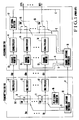
- Fig. 1 is a block diagram showing a basic arrangement of a non-interruption regular/standby channel switching system generally used in radio digital transmission.
- In Fig. 1, a transmitting
side 100 is connected to a receivingside 200 through n regular channels represented by CH₁ to CHn and a single standby channel represented by CHP. - The transmitting
side 100 comprises: switches 11 having the same arrangement and provided to the regular channels CH₁ to CHn to receive transmission signals IN₁ to INn;multiplexers 12 having the same arrangement and provided to the regular channels CH₁ to CHn and the standby channel CHP; apilot signal generator 16 for outputting a pilot signal; and a channel switching controller 18 for supplying a signal D to the switches 11 to control their switching operation. - When all the regular channels CH₁ to CHn are normal, none of the switches 11 are switched. Therefore, the pilot signal is output from the
pilot signal generator 16 to the channel CHP through aline 202. - If a fault occurs on one of the regular channels CH₁ to CHn, e.g., the channel CH₁, the switch 11 connected to the channel CH₁ is switched in accordance with the control signal D supplied from the channel switching controller 18, and a transmission signal of the channel CH₁ is supplied through the standby channel CHP.
- The
receiving side 200 comprises: channel monitors 13 for monitoring channel conditions of the standby channel CHP and the regular channels CH₁ to CHn and outputting a standby channel condition signal B and regular channel condition signals A;demultiplexers 14 for demultiplexing the output signals from thechannel monitors 13; switches 15 each for receiving the output signal from thedemultiplexer 14 of the standby channel CHP at its one input terminal, receiving the output signal from a corresponding one of thedemultiplexers 14 of the regular channels CH₁ to CHn at its other input terminal, and selecting one of the input signals in accordance with a control signal E; apilot signal detector 17 for detecting a pilot signal from the output signal from thedemultiplexer 14 of the standby channel CHP; and achannel switching controller 19 for outputting a switch control signal E for controlling theswitches 15 in accordance with the standby channel condition signal B from thechannel monitor 13 of the standby channel CHP, the regular channel condition signals A output from the channel monitors of the regular channels CH₁ to CHn, and the output signal C from thepilot signal detector 17, and transmitting a signal F representing switching demand to the channel switching controller 18 of the transmittingside 100. - A switching sequence of hitless switching in Fig. 1 is generally performed as follows. That is, if a fault occurs on, e.g., the regular channel CH₁, the channel monitor 13 of the channel CH₁ supplies the signal A representing the fault to the
channel switching controller 19. Thechannel switching controller 19 checks the presence/absence of the fault and the condition of the standby channel by using the standby channel condition signal B and the output signal C from thepilot signal detector 17 and then sends the switching demand signal to the channel switching controller 18 at the transmittingside 100. The channel switching controller 18 operates the switch 11 of the channel CH₁ by the channel switching signal D. - The
channel switching controller 19 at thereceiving side 200 compares the transmission signal from the regular channel CH₁ on which the fault occurs with the transmission signal from the standby channel. If it is determined that bits and phases of the two signals coincide with each other, the switching (hitless switching) signal E is supplied to theswitch 15. Theswitch 15 switches its input from thedemultiplexer 14 of the channel CH₁ to thedemultiplexer 14 of the standby channel CHP and outputs it as an output signal OUT1. As a result, switching from the channel CH₁ on which the fault occurs is completed. - Fig. 2 is a block diagram showing a partial detailed arrangement of the system shown in Fig. 1 for monitoring channel quality by the parity check method which is conventionally often used.
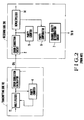
- At the transmitting
side 100 shown in Fig. 2, a transmission signal output from themultiplexer 12 is supplied to an error correction calculator 1 and to a parity counter 4. A count obtained by the parity counter 4 is supplied to themultiplexer 12 and inserted in a predetermined time slot. The output signal of themultiplexer 12 is subjected to error correction processing of the error correction calculator 1 and then output to a channel CHj (j = 1 to n). - At the
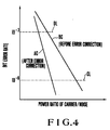
receiving side 200 shown in Fig. 2, a signal subjected to error correction by anerror correction circuit 2 is output to ademultiplexer 14 and a parity counter 5. The parity counter 5 performs parity counting similar to that of the parity counter 4 at the transmittingside 100 and outputs the count to a parity comparator 6. Thedemultiplexer 14 separates the parity inserted in the time slot by themultiplexer 12 at the transmittingside 100 and outputs the parity to the parity comparator 6. The parity comparator 6 compares the inputs from the parity counter 5 and thedemultiplexer 14 and outputs a parity error signal based on the comparison result. A channel quality determination circuit 7 performs quality determination of the channel in accordance with the parity error signal and outputs the determination information to thechannel switching controller 19. - However, since the channel quality monitoring using the parity bit in the conventional channel switching system is based on channel quality of a bit sequence after error correction, even if a large number of bit errors occur in the bit sequence before error correction, the bit errors of the bit sequence after error correction are maintained well. Therefore, according to the conventional method in which channel quality determination is performed by parity check after error correction, channel quality degradation caused by propagation path conditions cannot be detected in a short time period. In addition, as represented by a line AC in Fig. 4 showing an error rate characteristic before and after correction obtained when an error correction function is present, a degradation speed (speed of degradation in carrier wave power/noise ratio) is high, that is, for example, a time interval from an error rate 10⁻⁶ represented by a dotted line CL in Fig. 4 to system outage, e.g., an error rate 10⁻³ represented by a dotted line DL in Fig. 4 is short. Accordingly, a time usable for detecting information of channel degradation is short. As a result, system outage occurs before the transmission path is restored by channel switching.
- EP-A-225 643 discloses a channel switching system according to the preamble of claim 1 and without error correction.
- It is, therefore, an object of the present invention to eliminate the above drawback of the conventional technique and provide an apparatus capable of rapidly and reliably detecting a fault of a propagation path and restoring the propagation path by hitless switching in switching of a radio digital transmission system having an error correction function. This object is solved with the features of the claims.
- A (1+N) hitless channel switching system (N ≧ 1) of a digital transmission system having an error correction function according to the present invention comprises a detecting means, provided at a receiving side, for detecting a bit error rate before error correction, and a means for performing channel switching with non-interruption in accordance with the detected bit error rate.
- Fig. 1 is a block diagram showing a basic arrangement of a (1+N) hitless channel switching system common to a conventional technique and the present invention;
- Fig. 2 is a block diagram showing an arrangement according to the conventional technique of a part of the system shown in Fig. 1;
- Fig. 3 is a block diagram showing an arrangement according to an embodiment of the present invention; and
- Fig. 4 is a graph for explaining an operation and an effect of the present invention.
- An embodiment of the present invention will be described in detail below with reference to the accompanying drawings.
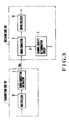
- Fig. 3 shows an arrangement of a main part of the embodiment of the present invention. In a system having an error correction function, at a transmitting
side 100, an output signal from amultiplexer 12 is supplied to an error correction calculator 1, and the error correction calculator 1 performs calculation in accordance with an error correction system. The calculation result is transmitted to a receivingside 200 using a time slot (redundant bit) through a corresponding channel CHj. At the receivingside 200, anerror correction circuit 2 corrects a bit error in a bit sequence before error correction using the error correction calculation result according to the error correction system and the contents of the redundant bit and outputs a signal subjected to error correction to ademultiplexer 14 and a signal G representing this bit error rate. At this time, the signal G representing the bit error rate is generated on the basis of channel quality of the bit sequence before error correction. Therefore, as shown by a line BC in Fig. 4, a time interval from channel quality degradation information detection (e.g., an error rate 10⁻⁶ point) to system outage (e.g., an error rate 10⁻³ point) is sufficient as compared with that in channel quality determination based on a bit sequence after error correction. - A channel
quality determination circuit 3 performs channel quality determination of the bit sequence before error correction by using the error correction control signal G and outputs a signal A representing channel quality degradation. - As has been described above, according to the present invention, even in the system having the error correction function, a switching apparatus can sufficiently follow a quality degradation speed of a propagation path because channel quality monitoring is performed before error correction.
Claims (2)
- A (1+N) (N ≧ 1) hitless channel switching system of a digital transmission system in which a transmitting side (100) is connected to a receiving side (200) through N regular channels and a single standby channel, comprising:
in said receiving side,a) means for detecting a bit error rate of each channelb) channel degradation determining means (3) for the regular channels; andc) switching means for switching the one regular channel where the degradation is detected to said standby channel
characterized byd) means (2) for performing an error correction; ande) wherein a degradation of the bit error rate is detected before the error correction takes place. - A (1+N) hitless channel switching system of a digital transmission system, in which a transmitting side (100) is connected to a receiving side (200) through N regular channels and a single standby channel, for transmitting N communication signals, comprising:
in said transmitting side (100),a) (N+1) multiplexers (12) connected to said N regular channels and said standby channel; and
in said receiving side (200),b) means for detecting bit error rates of said N regular channels and said standby channel;c) channel quality determining means (3) for determining qualities of said N regular channels and said standby channel; andd) switching means for switching a reception signal supplied through the one regular channel to a reception signal supplied through said standby channel and outputting the signal in response to the channel quality determining signal;
characterized in that
the transmitting side (100) comprises :
e) (N+1) error correction calculators (1) for performing error correction calculations of outputs from said (N+1) multiplexers (12) and outputting results of the error correction calculations to said (N+1) channels, respectively;f) channel switching means for causing, when a fault occurs on one of said N regular channels, said multiplexer (12) and said error correction calculators (1) connected to said standby channel to output the transmission signal corresponding to said regular channel on which the fault occurs, in response to a first control signal; andg) first control means for outputting the first control signal in response to a signal representing an occurrence of the fault supplied from said receiving side; and
the receiving side (200) comprises:h) error correcting means (2) for performing error corrections of reception signals supplied through said standby channel and said regular channels, respectively, to output corrected signals; andi) second control means for supplying the signal representing the switching demand to said transmitting side and outputting a second control signal in accordance with the signal output from said channel quality determining means.
Applications Claiming Priority (2)
| Application Number | Priority Date | Filing Date | Title |
|---|---|---|---|
| JP62248082A JPH084257B2 (en) | 1987-10-02 | 1987-10-02 | (1 + N) Hitless line switching device |
| JP248082/87 | 1987-10-02 |
Publications (3)
| Publication Number | Publication Date |
|---|---|
| EP0310110A2 EP0310110A2 (en) | 1989-04-05 |
| EP0310110A3 EP0310110A3 (en) | 1990-01-31 |
| EP0310110B1 true EP0310110B1 (en) | 1994-04-06 |
Family
ID=17172941
Family Applications (1)
| Application Number | Title | Priority Date | Filing Date |
|---|---|---|---|
| EP88116181A Revoked EP0310110B1 (en) | 1987-10-02 | 1988-09-30 | (1+N) hitless channel switching system |
Country Status (5)
| Country | Link |
|---|---|
| US (1) | US4961190A (en) |
| EP (1) | EP0310110B1 (en) |
| JP (1) | JPH084257B2 (en) |
| AU (1) | AU613093B2 (en) |
| DE (1) | DE3888909T2 (en) |
Cited By (1)
| Publication number | Priority date | Publication date | Assignee | Title |
|---|---|---|---|---|
| EP2066065A4 (en) * | 2006-09-22 | 2017-07-05 | NEC Corporation | Channel switch signal outputting circuit and channel switch signal outputting method |
Families Citing this family (25)
| Publication number | Priority date | Publication date | Assignee | Title |
|---|---|---|---|---|
| GB8813958D0 (en) * | 1988-06-13 | 1988-07-20 | Plessey Telecomm | Data path protection |
| JPH02149040A (en) * | 1988-11-30 | 1990-06-07 | Toshiba Corp | Data transmitting system |
| JPH0398318A (en) * | 1989-09-11 | 1991-04-23 | Fujitsu Ltd | Voice coding system |
| FR2653957A1 (en) * | 1989-10-27 | 1991-05-03 | Alcatel Transmission | Method and device for setting up switching requests in a digital transmission installation of "N+1" type, in which at least one main channel is equipped with an error correction device |
| JPH0456441A (en) * | 1990-06-25 | 1992-02-24 | Mitsubishi Electric Corp | Ring type local area network |
| JP3023705B2 (en) * | 1990-12-20 | 2000-03-21 | 富士通株式会社 | Spare channel switching apparatus and method |
| FR2670971A1 (en) * | 1990-12-21 | 1992-06-26 | Trt Telecom Radio Electr | SYSTEM FOR TRANSMITTING DATA WORDS USING AT LEAST TWO CHANNELS OF TRANSMISSION. |
| GB2267415B (en) * | 1992-05-19 | 1996-02-07 | Sony Broadcast & Communication | Signal switching |
| US5485465A (en) * | 1992-05-20 | 1996-01-16 | The Whitaker Corporation | Redundancy control for a broadcast data transmission system |
| JPH06224852A (en) * | 1993-01-25 | 1994-08-12 | Matsushita Electric Ind Co Ltd | Optical transmission system |
| DE4328523A1 (en) * | 1993-08-25 | 1995-03-02 | Telefunken Microelectron | Device for data transmission in low-voltage electrical systems |
| JP3179957B2 (en) * | 1994-02-28 | 2001-06-25 | 富士通株式会社 | Receiving apparatus and receiving signal output method in multimedia communication |
| EP0761049B1 (en) * | 1994-05-27 | 2000-08-30 | BRITISH TELECOMMUNICATIONS public limited company | Data communication system having channel switching means |
| US5742646A (en) * | 1995-05-05 | 1998-04-21 | Harris Corporation | Method of selecting and switching signal paths in a digital communication system |
| US7055081B2 (en) | 2001-03-02 | 2006-05-30 | Storage Technology Corporation | System and method for multi-channel decoding error correction |
| JP4300720B2 (en) * | 2001-06-29 | 2009-07-22 | Kddi株式会社 | Optical transmission system and line switching method |
| WO2003073423A1 (en) * | 2002-02-26 | 2003-09-04 | Storage Technology Corporation | System and method for multi-channel decoding error correction |
| JP4506452B2 (en) * | 2004-12-22 | 2010-07-21 | 日本電気株式会社 | Line switching apparatus and line switching method |
| JP4637769B2 (en) * | 2006-02-27 | 2011-02-23 | 京セラ株式会社 | Communication device |
| US8275071B2 (en) | 2007-05-17 | 2012-09-25 | Harris Stratex Networks Operating Corporation | Compact dual receiver architecture for point to point radio |
| US7782765B2 (en) * | 2007-01-22 | 2010-08-24 | Harris Stratex Networks Operating Corporation | Distributed protection switching architecture for point-to-point microwave radio systems |
| US8395256B2 (en) * | 2007-02-02 | 2013-03-12 | Harris Stratex Networks Operating Corporation | Packaging for low-cost, high-performance microwave and millimeter wave modules |
| US8095088B2 (en) | 2007-05-17 | 2012-01-10 | Harris Stratex Networks Operating Corporation | Compact wide dynamic range transmitter for point to point radio |
| JP2010183196A (en) * | 2009-02-03 | 2010-08-19 | Fujitsu Ltd | Data transfer system, data transmitting apparatus, data receiving apparatus, and data transfer method |
| JP2014027332A (en) * | 2012-07-24 | 2014-02-06 | Fujitsu Ltd | Transmission device |
Family Cites Families (15)
| Publication number | Priority date | Publication date | Assignee | Title |
|---|---|---|---|---|
| BE731482A (en) * | 1968-05-15 | 1969-09-15 | ||
| US4234956A (en) * | 1978-10-11 | 1980-11-18 | The General Electric Company Limited | Digital relay systems |
| FR2473819B1 (en) * | 1980-01-11 | 1985-12-13 | Telecommunications Sa | METHOD AND SYSTEM FOR SECURING A DIGITAL TRANSMISSION ARRES |
| JPS6077546A (en) * | 1983-10-05 | 1985-05-02 | Fujitsu Ltd | Supervising system of digital radio line |
| US4744083A (en) * | 1984-09-14 | 1988-05-10 | Geostar Corporation | Satellite-based position determining and message transfer system with monitoring of link quality |
| JPS61111036A (en) * | 1984-11-05 | 1986-05-29 | Nec Corp | Synchronizing switching system |
| JPS61111037A (en) * | 1984-11-05 | 1986-05-29 | Nec Corp | Line switch system |
| FR2574237B1 (en) * | 1984-11-30 | 1992-05-22 | Telecommunications Sa | SWITCHING SYSTEM FOR A DIGITAL TRANSMISSION NETWORK |
| JPS61283241A (en) * | 1985-06-10 | 1986-12-13 | Nec Corp | Data communication receiver |
| JPS6288450A (en) * | 1985-10-14 | 1987-04-22 | Nec Corp | Line supervisory system |
| CA1249633A (en) * | 1985-12-11 | 1989-01-31 | Hideaki Morimoto | Channel switching system |
| JPS62181533A (en) * | 1986-02-05 | 1987-08-08 | Nec Corp | Radio wave receiving equipment |
| DE3788532T2 (en) * | 1986-03-31 | 1994-04-21 | Nec Corp | Radio transmission system with simplified error correction circuit and fast channel switching. |
| JPS6333028A (en) * | 1986-07-26 | 1988-02-12 | Nec Corp | Signal detection system |
| JPS6377235A (en) * | 1986-09-20 | 1988-04-07 | Fujitsu Ltd | Switching system for digital communication system |
-
1987
- 1987-10-02 JP JP62248082A patent/JPH084257B2/en not_active Expired - Lifetime
-
1988
- 1988-09-30 EP EP88116181A patent/EP0310110B1/en not_active Revoked
- 1988-09-30 DE DE3888909T patent/DE3888909T2/en not_active Revoked
- 1988-10-03 US US07/251,643 patent/US4961190A/en not_active Expired - Lifetime
- 1988-10-04 AU AU23389/88A patent/AU613093B2/en not_active Expired
Cited By (1)
| Publication number | Priority date | Publication date | Assignee | Title |
|---|---|---|---|---|
| EP2066065A4 (en) * | 2006-09-22 | 2017-07-05 | NEC Corporation | Channel switch signal outputting circuit and channel switch signal outputting method |
Also Published As
| Publication number | Publication date |
|---|---|
| US4961190A (en) | 1990-10-02 |
| AU2338988A (en) | 1989-04-06 |
| JPH0191544A (en) | 1989-04-11 |
| AU613093B2 (en) | 1991-07-25 |
| DE3888909T2 (en) | 1994-07-21 |
| JPH084257B2 (en) | 1996-01-17 |
| DE3888909D1 (en) | 1994-05-11 |
| EP0310110A3 (en) | 1990-01-31 |
| EP0310110A2 (en) | 1989-04-05 |
Similar Documents
| Publication | Publication Date | Title |
|---|---|---|
| EP0310110B1 (en) | (1+N) hitless channel switching system | |
| US5577196A (en) | Intelligent digital signal hitless protection switch | |
| US20030037297A1 (en) | Frame synchronization device and frame synchronization method | |
| EP0225643B1 (en) | Channel switching system | |
| JPH07177116A (en) | Digital signal transmitter | |
| JP3308908B2 (en) | Transmission system | |
| US6870859B1 (en) | Multiplexing system and multiplexing method of tributary signals | |
| JPH05145531A (en) | Uninterruptible line changeover device | |
| JP2616695B2 (en) | Line switching device | |
| JPH0620193B2 (en) | Line monitoring method | |
| JPS6216589B2 (en) | ||
| JP2867495B2 (en) | Hitless switching method | |
| JPH02285830A (en) | Synchronizing changeover device | |
| JP4506452B2 (en) | Line switching apparatus and line switching method | |
| JPH05291982A (en) | Line switching system | |
| JP2010093517A (en) | Line quality detection device, line quality detecting method and line switching device using the same, and line switching method | |
| JPH0746226A (en) | Error monitor circuit | |
| JPH01149634A (en) | Line switching device | |
| JPH01273445A (en) | Multiplex transmission system | |
| US20050111373A1 (en) | Node device | |
| JPH0951362A (en) | Data reloading system | |
| JPS61111036A (en) | Synchronizing switching system | |
| JPH01180150A (en) | Control line transmission system | |
| JPS61144942A (en) | Line switching system in loop data transmission line | |
| JPH04122127A (en) | System switching information transfer system for optical submarine cable system |
Legal Events
| Date | Code | Title | Description |
|---|---|---|---|
| PUAI | Public reference made under article 153(3) epc to a published international application that has entered the european phase |
Free format text: ORIGINAL CODE: 0009012 |
|
| 17P | Request for examination filed |
Effective date: 19880930 |
|
| AK | Designated contracting states |
Kind code of ref document: A2 Designated state(s): DE GB SE |
|
| PUAL | Search report despatched |
Free format text: ORIGINAL CODE: 0009013 |
|
| AK | Designated contracting states |
Kind code of ref document: A3 Designated state(s): DE GB SE |
|
| 17Q | First examination report despatched |
Effective date: 19920221 |
|
| GRAA | (expected) grant |
Free format text: ORIGINAL CODE: 0009210 |
|
| AK | Designated contracting states |
Kind code of ref document: B1 Designated state(s): DE GB SE |
|
| REF | Corresponds to: |
Ref document number: 3888909 Country of ref document: DE Date of ref document: 19940511 |
|
| PLBI | Opposition filed |
Free format text: ORIGINAL CODE: 0009260 |
|
| EAL | Se: european patent in force in sweden |
Ref document number: 88116181.4 |
|
| 26 | Opposition filed |
Opponent name: SIEMENS AG Effective date: 19950105 |
|
| PLBQ | Unpublished change to opponent data |
Free format text: ORIGINAL CODE: EPIDOS OPPO |
|
| PLAB | Opposition data, opponent's data or that of the opponent's representative modified |
Free format text: ORIGINAL CODE: 0009299OPPO |
|
| R26 | Opposition filed (corrected) |
Opponent name: SIEMENS AG Effective date: 19950105 |
|
| RDAH | Patent revoked |
Free format text: ORIGINAL CODE: EPIDOS REVO |
|
| APAC | Appeal dossier modified |
Free format text: ORIGINAL CODE: EPIDOS NOAPO |
|
| APAE | Appeal reference modified |
Free format text: ORIGINAL CODE: EPIDOS REFNO |
|
| APAC | Appeal dossier modified |
Free format text: ORIGINAL CODE: EPIDOS NOAPO |
|
| PGFP | Annual fee paid to national office [announced via postgrant information from national office to epo] |
Ref country code: SE Payment date: 20010918 Year of fee payment: 14 |
|
| PGFP | Annual fee paid to national office [announced via postgrant information from national office to epo] |
Ref country code: GB Payment date: 20011003 Year of fee payment: 14 |
|
| APAC | Appeal dossier modified |
Free format text: ORIGINAL CODE: EPIDOS NOAPO |
|
| PGFP | Annual fee paid to national office [announced via postgrant information from national office to epo] |
Ref country code: DE Payment date: 20011015 Year of fee payment: 14 |
|
| RDAG | Patent revoked |
Free format text: ORIGINAL CODE: 0009271 |
|
| STAA | Information on the status of an ep patent application or granted ep patent |
Free format text: STATUS: PATENT REVOKED |
|
| 27W | Patent revoked |
Effective date: 20011012 |
|
| GBPR | Gb: patent revoked under art. 102 of the ep convention designating the uk as contracting state |
Free format text: 20011012 |
|
| APAH | Appeal reference modified |
Free format text: ORIGINAL CODE: EPIDOSCREFNO |