EP0312652A1 - Optical device with phase-locked diodelaser array - Google Patents
Optical device with phase-locked diodelaser array Download PDFInfo
- Publication number
- EP0312652A1 EP0312652A1 EP87201996A EP87201996A EP0312652A1 EP 0312652 A1 EP0312652 A1 EP 0312652A1 EP 87201996 A EP87201996 A EP 87201996A EP 87201996 A EP87201996 A EP 87201996A EP 0312652 A1 EP0312652 A1 EP 0312652A1
- Authority
- EP
- European Patent Office
- Prior art keywords
- prism
- radiation
- optical
- optical device
- array
- Prior art date
- Legal status (The legal status is an assumption and is not a legal conclusion. Google has not performed a legal analysis and makes no representation as to the accuracy of the status listed.)
- Granted
Links
Images


Classifications
-
- G—PHYSICS
- G11—INFORMATION STORAGE
- G11B—INFORMATION STORAGE BASED ON RELATIVE MOVEMENT BETWEEN RECORD CARRIER AND TRANSDUCER
- G11B7/00—Recording or reproducing by optical means, e.g. recording using a thermal beam of optical radiation by modifying optical properties or the physical structure, reproducing using an optical beam at lower power by sensing optical properties; Record carriers therefor
- G11B7/08—Disposition or mounting of heads or light sources relatively to record carriers
-
- G—PHYSICS
- G02—OPTICS
- G02B—OPTICAL ELEMENTS, SYSTEMS OR APPARATUS
- G02B19/00—Condensers, e.g. light collectors or similar non-imaging optics
- G02B19/0033—Condensers, e.g. light collectors or similar non-imaging optics characterised by the use
- G02B19/0047—Condensers, e.g. light collectors or similar non-imaging optics characterised by the use for use with a light source
- G02B19/0052—Condensers, e.g. light collectors or similar non-imaging optics characterised by the use for use with a light source the light source comprising a laser diode
- G02B19/0057—Condensers, e.g. light collectors or similar non-imaging optics characterised by the use for use with a light source the light source comprising a laser diode in the form of a laser diode array, e.g. laser diode bar
-
- G—PHYSICS
- G02—OPTICS
- G02B—OPTICAL ELEMENTS, SYSTEMS OR APPARATUS
- G02B19/00—Condensers, e.g. light collectors or similar non-imaging optics
- G02B19/0004—Condensers, e.g. light collectors or similar non-imaging optics characterised by the optical means employed
- G02B19/0009—Condensers, e.g. light collectors or similar non-imaging optics characterised by the optical means employed having refractive surfaces only
- G02B19/0014—Condensers, e.g. light collectors or similar non-imaging optics characterised by the optical means employed having refractive surfaces only at least one surface having optical power
-
- G—PHYSICS
- G02—OPTICS
- G02B—OPTICAL ELEMENTS, SYSTEMS OR APPARATUS
- G02B27/00—Optical systems or apparatus not provided for by any of the groups G02B1/00 - G02B26/00, G02B30/00
- G02B27/09—Beam shaping, e.g. changing the cross-sectional area, not otherwise provided for
-
- G—PHYSICS
- G02—OPTICS
- G02B—OPTICAL ELEMENTS, SYSTEMS OR APPARATUS
- G02B27/00—Optical systems or apparatus not provided for by any of the groups G02B1/00 - G02B26/00, G02B30/00
- G02B27/09—Beam shaping, e.g. changing the cross-sectional area, not otherwise provided for
- G02B27/0938—Using specific optical elements
- G02B27/095—Refractive optical elements
- G02B27/0972—Prisms
-
- G—PHYSICS
- G02—OPTICS
- G02B—OPTICAL ELEMENTS, SYSTEMS OR APPARATUS
- G02B27/00—Optical systems or apparatus not provided for by any of the groups G02B1/00 - G02B26/00, G02B30/00
- G02B27/28—Optical systems or apparatus not provided for by any of the groups G02B1/00 - G02B26/00, G02B30/00 for polarising
-
- G—PHYSICS
- G11—INFORMATION STORAGE
- G11B—INFORMATION STORAGE BASED ON RELATIVE MOVEMENT BETWEEN RECORD CARRIER AND TRANSDUCER
- G11B7/00—Recording or reproducing by optical means, e.g. recording using a thermal beam of optical radiation by modifying optical properties or the physical structure, reproducing using an optical beam at lower power by sensing optical properties; Record carriers therefor
- G11B7/12—Heads, e.g. forming of the optical beam spot or modulation of the optical beam
- G11B7/125—Optical beam sources therefor, e.g. laser control circuitry specially adapted for optical storage devices; Modulators, e.g. means for controlling the size or intensity of optical spots or optical traces
- G11B7/127—Lasers; Multiple laser arrays
-
- G—PHYSICS
- G11—INFORMATION STORAGE
- G11B—INFORMATION STORAGE BASED ON RELATIVE MOVEMENT BETWEEN RECORD CARRIER AND TRANSDUCER
- G11B7/00—Recording or reproducing by optical means, e.g. recording using a thermal beam of optical radiation by modifying optical properties or the physical structure, reproducing using an optical beam at lower power by sensing optical properties; Record carriers therefor
- G11B7/12—Heads, e.g. forming of the optical beam spot or modulation of the optical beam
- G11B7/135—Means for guiding the beam from the source to the record carrier or from the record carrier to the detector
- G11B7/1359—Single prisms
-
- G—PHYSICS
- G11—INFORMATION STORAGE
- G11B—INFORMATION STORAGE BASED ON RELATIVE MOVEMENT BETWEEN RECORD CARRIER AND TRANSDUCER
- G11B7/00—Recording or reproducing by optical means, e.g. recording using a thermal beam of optical radiation by modifying optical properties or the physical structure, reproducing using an optical beam at lower power by sensing optical properties; Record carriers therefor
- G11B7/12—Heads, e.g. forming of the optical beam spot or modulation of the optical beam
- G11B7/135—Means for guiding the beam from the source to the record carrier or from the record carrier to the detector
- G11B7/1395—Beam splitters or combiners
-
- G—PHYSICS
- G11—INFORMATION STORAGE
- G11B—INFORMATION STORAGE BASED ON RELATIVE MOVEMENT BETWEEN RECORD CARRIER AND TRANSDUCER
- G11B7/00—Recording or reproducing by optical means, e.g. recording using a thermal beam of optical radiation by modifying optical properties or the physical structure, reproducing using an optical beam at lower power by sensing optical properties; Record carriers therefor
- G11B7/12—Heads, e.g. forming of the optical beam spot or modulation of the optical beam
- G11B7/135—Means for guiding the beam from the source to the record carrier or from the record carrier to the detector
- G11B7/1398—Means for shaping the cross-section of the beam, e.g. into circular or elliptical cross-section
Definitions
- the invention relates to an optical device for delivering a single radiation beam, comprising a phase-locked diodelaser array and a collimatorlens, which laser array radiates in a stable supermode having, in a lateral plane through the axis of symmetry of the radiation and parallel to the pn-junction layer of the laser array, two far field lobes.
- the invention also relates to an apparatus for scanning an information medium, such as an optical disc recorder and/or player or a laser printer, comprising such optical device.
- phase-locked diodelaser array which is a special kind of multi-emitter semiconductor laser.
- phase-locked diodelasers Because they can deliver a considerably higher output power than a single-emitter diodelaser.
- Such focussing cannot be carried out by a high-aperture objective lens solely, because of the specific radiation pattern of the phase-locked laser array.
- Such an array with N emitters radiates in N so-called supermodes, and the laser itself selects that or those, supermode(s) for which its treshold current is minimum.
- the treshold current is the value of the electric current perpendicular to the p-n junction layer at which the laser action starts.
- the specific internal structure of a diodelaser array determines the favoured radiation mode of this array.
- the so-called highest order supermode may be the favoured one.
- the radiation of each emitter is ⁇ rad. out of phase with that of its two neighbour emitters. Because of this phase shift the highest order supermode is stable up to high power.
- the diodelaser array may also radiate in other supermodes which are also stable.
- a stable supermode is such one for which at every time the radiation of some emitters have a first phase which is ⁇ rad. different from a second phase which the radiations of the other emitters have of that time.
- the terms "near field phase- or intensity distribution” and "far field phase- or intensity distribution” are used.
- the former is the distribution at the position of the emitting facet of the diodelaser array, or in a plane conjugate to this facet.
- the far field phase- or intensity distribution is the result of the interference of the individual beams emanating from the individual slit-shaped emitters of the array.
- the far field distribution is formed at some distance from the emitting facet.
- the near-and far field in this application are reserved for those fields in the lateral plane, i.e. the plane through the aixs of the radiation pattern and parallel to the pn-junction layer.
- the plane perpendicular to the said layer and through said axis is the transversal plane.
- optical device with a phase-locked diodelaser array radiating in a stable supermode and delivering a single radiation beam.
- This optical device is characterized in, that behind the collimatorlens are arranged, in this order, a polarisation rotator in the path of one of the lateral lobes and a polarisation-sensitive beam combiner in the paths of both lateral far field lobes.
- the polarisation rotator changes the polarisation direction of the radiation of one of the lobes, such that this direction becomes perpendicular to that of the radiation of the other lobe.
- the polarisation-sensitive beam combiner in the form of a composed birefringent element, combines the radiations of the two lobes in one lobe. Because the radiations of the two lobes have mutually perpendicular polarisation directions these radiations do not interfere with each other. This principle of lobe superposition in a laser array device can be realized with different embodiments.
- the first embodiment is characterized in, that the beam combiner is a prism of Wollaston, and in that between the polarisation rotator and the prism of Wollaston a composed beam deflector is arranged for directing the axes of the radiations of the two lobes such as to intersect at the prism of Wollaston.
- the composed beam deflector preferably is a double optical wedge. Compared with a system of for example separate mirrors, such wedge has the advantage of being simple and easy to assemble in the device.
- a prism of Wollaston can be composed of two component prisms of uniaxial birefringent material and having mutually perpendicular optical axes. Such a composed prism can combine the radiations of two lobes for which the angle between the axes of the lobes does not exceed a certain value.
- the said first embodiment is preferably further characterized in, that the prism of Wollaston comprises three component prisms of birefringent material arranged after each other, the two outer component prism having the same optical axis and substantially the same shape and dimensions, while the central component prism has a different shape and different dimensions and an optical axis perpendicular to the optical axis of the outer component prisms.
- This prism of Wollaston can deflect an incident beam under larger angles than a two-component prism of Wollaston and moreover has the advantage of being symmetric.
- a second embodiment of the optical device is characterized in, that the polarisation-sensitive beam combiner comprises a first and a second birefringent plate which are parallel to each other, the optical axes of the plates having different directions each at 45 degrees with the plate surfaces and crossing each other.
- Savart Plate or Savart Polariscope
- Savart Polariscope does not only combine the two lobes into one single lobe but also bends the axes of the two lobes towards each other. Thus, up to a certain value of the angle between the axes of the lobes, no separate beam deflector is needed.
- the said second embodiment may be further characterized in, that a beam deflector is arranged between the collimatorlens and the first birefringent plate.
- the second embodiment may be further characterized in, that between the first and second birefringent plate a ⁇ /2-plate is arranged wherein ⁇ is the wavelength of the diodelaser radiation.
- This ⁇ /2-plate rotates the polarisation direction of the radiation from the first plate before it enters the second plate.
- the Savart-plate can deflect over larger angles, so that also two diodelaser lobes which, at the entrance face of the Savart-plate, have a larger mutual distance can be superposed.
- the radiation pattern of the laserdiode array also has side lobes.
- the wavefront of the diodelaser array is astigmatic and the dimension of the radiation pattern in the lateral plane is considerably smaller than that in the transversal plane.
- a device which delivers a single high intensity radiation beam with circular cross-section and free of astigmatism is preferably further characterized in, that behind the polarisation-sensitive beam combiner are arranged, in this order, a prism system of at least one prism having in the lateral plane an entrance face inclined with respect to the axis of the incident radiation and an exit face perpendicular to the axis of the emergent radiation, and a spatial filter in the lateral far field of the diodelaser array.
- the prism system broadens the central lobe in the lateral plane so that its lateral width becomes equal to the transversal width.
- the spatial filter blocks the unwanted lobes and transmits only the enlarged central lobe.
- the prism system also has a de-astigmatic effect.
- the collimatorlens is so dimensioned and arranged that some wavefront sphericity remains in the beam, especially in the lateral plane.
- This prism will impart astigmatism to the beam.
- the astigmatic effect of the prism system is used to correct for the astigmatism of the diodelaser array.
- the prism system could also be performed by an arrangement of cylindrical lenses.
- the prism system however has the advantage that it is compact and less sensitive to tilting or shifting with respect to the optical axis of the device.
- the prism system may comprise one prism, two prisms of four prisms.
- the enlargement power of the prisms is reduced, so that less stringent requirements are to be set to the alignment and the tolerance of the prisms.
- the enlargement power of the prism system is increased. This is of importance when the number of radiating stripes in the diodelaser array is increased.
- the invention may advantageously be used in an apparatus for optically recording an optical record carrier and comprising an optical head for generating a radiation spot modulated in intensity according to the information to be recorded, because of the relative high recording intensity involved.
- This apparatus is characterized in, that the optical head comprises an optical device as described hereinbefore and an objective lens for focussing the beam from said device into a diffraction-limited round spot on the record carrier.
- the invention may also be used in an apparatus for reading a record carrier and comprising an optical head wherein a radiation spot for scanning the record carrier is generated.
- This apparatus is characterized in, that the optical head comprises an optical device as described hereinbefore and an objective lens for focussing the beam from said device into a diffraction-limited round spot on the record carrier.
- the invention may also be used advantageously in an apparatus for laser printing information on a recording-medium comprising a recording medium carrier movable in a first direction and a beam deflector for scanning a radiation beam along a second direction perpendicular to the first direction.
- This apparatus is characterized in, that it comprises an optical device as described hereinbefore for generating a substantially collimated beam that is focussed by an objective lens to a diffraction-limited radiation spot on the recording medium.
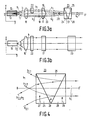
- FIG. 1 shows schematically and in perspective view a multi-emitter semiconductor diodelaser, a so-called phase-locked laser array.
- This diodelaser comprises, amongst others, a first layer 11 of p-type material, a second layer 12 of n-type material and an intermediate layer 13, or pn-junction layer, wherein the laser action takes place when an electric current above a certain treshold value is send through the laser unit in the Z-direction.
- the laser radiation emanates through the front facet, or cleaved surface, 14 of the layer 13 and propagates in the Y-direction .
- This radiation shows a first, small, divergence in the XY-plane, called the lateral plane, and a second, greater, divergence in the YZ-plane, called the transversal plane.
- the pn-junction layer comprises a number of radiation guiding stripes 131, 132, etc. which are separated from each other by intermediate stripes. For clearness sake in Figure 1 only four guiding stripes are shown but their number may amount to ten or more.
- a phase-locked laser array provides the advantage of a considerably increased power output relative to a single emitter diodelaser, so that the laser array is very well suited to record information on an optical medium like an optical disc or the recording medium of a laser printer.
- the radiation of all of the individual emitters 141, 142, etc. should then be concentrated into a single, round and diffraction-limited radiation spot.
- additional optical elements are needed, because of the specific radiation pattern of a diodelaser array.
- an N-emitter laser array can be so constructed that it radiates in the highest order supermode. In this mode the adjacent stripes radiate in anti-phase. This mode is very stable up to high power, but the far field radiation pattern comprises two central lobes insted of one.
- Figure 2 the intensity-and phase distribution of a phase-locked diodelaser array in the near-field and far field are shown. For the sake of simplicity a two-emitter array is taken.
- Figure 2a gives the intensity (I) distribution
- the phase is given for different times (t).
- the intensity, respectively phase, distribution in the far field is shown in Figures 2c and 2d respectively.
- the diodelaser array may also radiate into other stable modes which also have a dual lobe far-field pattern.
- dual lobe pattern is obtained when the radiation of some of the emitters shows a phase difference of ⁇ rad. with that of the remaining emitters.
- a single spot of the stable diodelaser array could be obtained if one of the lobes would be blocked. But then half of the radiation energy is lost. Accordingly to the present invention the radiations of the two lobes are united into one lobe.
- FIG. 3a A first embodiment of the device according to the invention is shown in Figure 3a and Figure 3b in lateral and transversal section respectively.
- the diodelaser array with radiation guiding stripes 13 This array emits a radiation pattern which in the transversal plane is a single beam b with opening angle ⁇ 2.
- the radiation pattern In the lateral plane the radiation pattern has an opening angle ⁇ 1 and at some distance from the laser facet, so in the far-field, it is composed of two radiation lobes l1 and l2.
- a collimatorlens 16 is arranged, which provisionally for facilitating the description is supposed to collimate the radiation both in the transversal and lateral plane, so that in the lateral plane the two radiation lobes are coverted into two collimated subbeams b1 and b2.
- These beams pass through an optical element 17 which in the lateral plane has the shape of a double wedge with a plane entrance face 18 and two inclined exit faces 19 and 20 for the subbeams b1 and b2 respectively. At the latter faces refraction occurs so that the subbeams are broken towards the optical axis 00 ⁇ of the device.
- the deflected subbeams overlap each other in a plane 21.
- the chief rays h1 and h2 of the subbeams b1 and b2 make an angle 2 ⁇ with each other, so that behind the plane 21 these beams would again diverge from each other.
- the chief rays h1 and h2 are made to coincide by using polarisation-sensitive optics in the form of a ⁇ /2-plate 22 and a prism of Wollaston 23.
- the ⁇ /2-plate wherein ⁇ is the wavelength of the radiation, rotates the polarisation direction of the subbeam b1 so that it becomes perpendicular to the plane of the drawing when the radiation emitted by the diodelaser array is linearly polarised with the polarisation direction parallel to the plane of the drawing.
- the prism of Wollaston may comprise two component prisms which are triangular shaped and consist of an uniaxial birefringent material like quartz. The optic axes of the component prism are perpendicular to each other.
- such a prism of Wollaston deflects an incident beam under either one of two equal but opposite angles depending upon whether the polarisation direction of this beam is parallel or perpendicular to the optic axis of one of the component prisms.
- the prism of Wollaston can bend these chief rays so that both chief rays become coincident with the optical axis 00 ⁇ of the device.
- the embodiment of Figure 3a comprises a special kind of prism of Wollaston.
- This prism and the paths of the beams b1 and b2 through it are shown in more detail in Figure 4.
- the prism consists of three component prisms 24, 25 and 26 of uniaxial briefringent material.
- the outer component prisms 24 and 26 have the same shape and dimensions and their optical axis 27 and 29 are parallel to each other and to the plane of the drawing.
- the central component prism has another shape and dimensions and its optical axis 28 is perpendicular to the plane of the drawing.
- the boundary rays b 1,1 , b 1,2 of the beams b1 passes through it as ordinary rays
- the boundary rays b 2,1 , b 2,2 of the beam b2 pas through it as extra-ordinary rays.
- Whether a ray is ordinary or extra-ordinary depends on the polarisation direction of the beam with respect to the direction of the optical axis of the said component prism.
- the orientation of the boundary faces of the component prisms and their ordinary and extra-ordinary refractive indices can be chosen such that the beams b1 and b2 coincide after passage through the composed prism.
- the prism of Wollaston of Figure 4 with three component prisms can deflect an incident beam under larger angles than a prism of Wollaston with two component prisms.
- the Figure 4 prism of Wollaston has a symmetric construction.
- a further advantage of the prism of Figure 4 is that the component prisms 24 and 26 which have the same optical axis also have the same shape while the component prism 25 with a different direction of the optical axis also has a different shape. This prevents that during assembling of the composed prism 23 the component prisms with different optical axis might be interchanged.
- a prism of Wollaston instead of a prism of Wollaston also other composed prisms having component prisms of birefringent material and different optical axis, like a prism of Rochon, may be used.
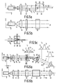
- Figures 5a and 5b show a second embodiment of the optical device in lateral and transversal section respectively.
- This embodiment differs from that of Figures 3a and 3b in that the double wedge and the prism of Wollaston are replaced by a single composed element known as a Savart-plate or -polariscope.
- This element 30 consists of a first and a second plane parallel plate, 31 and 32 respectively, of uniaxiale birefringent material for example quartz.
- the optical axis 33, respectively 34, of plates 31 and 32 are at an angle of 45 degrees with the plane surfaces, whereby axis 33 is perpendicular to axis 34.
- a Savart-plate can superpose two beams with mutually perpendicular polarisation directions.
- the beam b2 is consequently deflected in plane 31 and passes undeflected through plate 32.
- both beams have the same polarisation direction and consequently are passed through the plate 32 in the same way.
- the beam b2 becomes coincident with beam b1.
- the two-component Savart-plate of Figure 5a can superpose two mutually perpendicular polarised beams which are at not to large mutual distance.
- the modified Savart configuration 30 ⁇ shown in Figure 5c can be used.
- This configuration is different from the configuration 30 in Figure 5a in that ⁇ /2-plate 35 is arranged between the plates 31, 32.
- This plate 35 rotates the polarisation directions of the beams b1 and b2 from the plate 31 over 90 degrees before they enter the plate 32.
- the beam b1 is then an extra-ordinary beam in the lateral plane for the plate 32 and is deflected towards beam b2.
- the effective angle over which the beams are deflected towards each other is twice that over which an unmodified Savart-plate can deflect.
- the radiation pattern emerging from the Savart-configuration in Figure 5a or 5c or from the prism of Wollaston in Figure 3a and 3b is in principle suited to be focussed into one spot.
- this radiation pattern has besides a central lobe also side lobes which, upon focussing of the radiation pattern, may intefere with the central lobe thereby generating an interference pattern of dark and light areas in the spot.
- the laser array has a linear shaped emitter; an array of ten emitters for example measures 40 ⁇ m x 2 ⁇ m.
- the aperture of the composed beam emitted by the diodelaser array is relative small in the lateral plane and relative large in the transversal plane. Downstream from the emitting facet the composed radiation beam has an elliptical cross-section and for obtaining a round spot the beam should be reshaped so that its cross-section becomes circular.
- the radiation from the prism of Wollaston or from the Savart-plate can be formed into a beam which is suited to be focussed into a single, round and diffraction-limited spot by enlarging the radiation pattern in the lateral plane and by filtering the central lobe, whereby the functions of enlarging, beam shaping and astigmatism elimination can be performed by one and the same prism system.
- the Figures 6a and 6b show, in lateral and transversal section respectively, a first embodiment of such prism system 40 in combination with the optical device of Figures 5a and 5b.
- the lens power and the axial position of the collimatorlens 16 are chosen such that it nearly collimates the beam b c in the transversal plane.
- the wavefront of the beam b c after passage through the lens 16 is more curved, due to the ⁇ y shift of the point of origin 01 in this plane.
- the prism 40 arranged behind the Savart-plates 30 ⁇ only slightly affects the beam in the transversal plane, because in this plane the beam is nearly perpendicular to the entrance face 41 and the exit face 42 of the prism.
- the entrance face 43 is arranged at an angle ⁇ with the axis h c of the beam.
- refraction occurs such that the beam is widened, in dependency of the angle ⁇ .
- Behind the prism 40 a diaphragm 45 is arranged. The opening of this diaphragm and the orientation and parameters of the prism 40 are so adapted to each other that the diaphragm passes only the central lobe 10 of the radiation pattern and blocks all of the sides lobes 11, 11 etc.
- the prism Because in the lateral plane the beam passing through the skew prism is not collimated, the prism imparts astigmatism to the beam. It can be arranged such that this astigmatism compensates the astigmatism of the diodelaser array, so that the wavefront of the beam from the prism has the same curvature in the lateral and transversal planes.
- the angle ⁇ between the faces 44 and 45 of the prism 40 may have an arbitrary value. In practice it is preferred that this angle is 90 degrees becauseee of easier manufacturing and assembling.
- the first of these embodiments is shown in Figures 7a and 7b, in lateral and transversal cross-section respectively, and comprises two prisms 50 and 54.
- a second prism By using a second prism it becomes possible to bend the axis h c ⁇ back so that it is parallel to the axis of h of the incident radiation.
- the transversal dimension of the device is decreased, which is of importance especially when the device is to be used in optical disc recorder/player.
- less beam widening power for each prism is needed so that less stringent requirements are to be set to the alignment and the tolerances of the prisms.
- Figures 8a and 8b shows the embodiment of the optical device with four prisms 60, 61, 62 and 63. Besides that the beam-widening power needed for each prism if further reduced, the embodiment has the advantage that axis h c ⁇ of the emergent radiation is coincident with axis h of the incident radiation, so that the device can be housed is a small tubular holder.
- the beam widening power is preferably equally divided over the prisms.
- the prisms preferably have the same shape and dimensions, which considerably decreases the manufacturing costs of the device.
- the spatial filter may be constituted by a separate element (45) in the form of a diaphragm on a separate holder. It is also possible that such diaphragm is fixed to the exit face 44, respectively 56, of the last prism in the embodiments of Figures 6 and 7 respectively and of Figure 8. As indicated in Figure 7a it is also possible to apply an opaque coating 57, leaving a central opening, on said faces. Another possibility is that the boundaries of said last prism form a natural stop for the radiation towards further optical elements of the optical apparatus, as indicated in Figure 7a by the interrupted lines 58, 59. Finally in an apparatus wherein the spot forming lens 46 is arranged close to the last prism (63, 54, 40) of the prism system, the spatial filter may be formed by the pupil of the spot lens, as indicated by 64 in Figures 8a and 8b.
- Figure 9 shows schematically an apparatus for recording information in a surface 71 of an optical record carrier 70.
- the surface 71 may be provided with pregrooved servo tracks 72.
- the laser unit preferably is phase-locked diodelaser array designated 10, emits a beam b which should be focussed by an objective lens 46 to a high-intensity, round an diffraction-limited, radiation spot S on the information surface 71.
- the laser array 10 and the objective lens 46 and unit 80 comprising a collimator lens 16 and a system of for example a beam deflector 17 and a prism of Wollaston 23, or a Savart-plate, as shown in Figures 3, 4 and 5, which may be combined with a prism- and spatial filter system 81, as shown in Figures 6, 7 and 8 is arranged to convert the radiation form the laser array into a collimated, rotationally symmetrical, beam.
- Recording of an information track is performed by modulating the beam intensity in accordance with the information to be recorded and by rotating the record carrier around its axis 73.
- a finel control of the spot S relative to a track can be performed by a mirror 74 which is pivotable in the direction of arrow 75.
- Modulation of the recording beam can be performed for example by modulating the electric current through the laser array 10.
- the apparatus of Figure 9 can be used for reading the information recorded on the record carrier.
- a beam separator for example a beam splitting prism 76
- the unit 80 which separator directs part of the beam reflected from the record carrier, for example via a lens 77, towards a photosensitive detector 78
- the apparatus of Figure 9 can be used for reading the information recorded on the record carrier.
- the beam has a constant intensity of such level that it cannot provoke any change in the recording surface.
- Figure 10 shows schematically a laser printer with a recording medium 91, for example wrapped around a drum 90 which, for recording successive lines, is rotated around its axis 92.
- Line scanning is performed for example by a polygon 93 carrying a number of mirror facets 94 and rotating around its axis 95.
- 46 is an objective lens which should focus the radiation from a phase-locked diodelaser array 10 and reflected by a facet 94 to a round spot S of small diameter on the recording medium.
- the laser beam is modulated in intensity according to the information to be recorded, either by the electric current through the laser array or by a separate modulator in the path of the beam.
- a block 80 comprising a collimatorlens 16 and a system of for example a beam deflector 17 and a Savart-configuration 30 ⁇ , or a prism of Wollaston, as shown in Figures 3, 4 and 5, which may be combined with a prism- and spatial filter system 81, as shown in Figures 6, 7 and 8, is arranged between the laser array 10 and the objective lens 46.
- the invention can be used in all apparatuses wherein a high intensity small and round spot should be formed out of the radiation of a phase-locked diodelaser array.
- a projection TV-apparatus with light halves or Liquid Chrystal Displays for modulating the laser radiation with (colour) TV information can be mentioned.
- the present invention can be used.
Abstract
Description
- The invention relates to an optical device for delivering a single radiation beam, comprising a phase-locked diodelaser array and a collimatorlens, which laser array radiates in a stable supermode having, in a lateral plane through the axis of symmetry of the radiation and parallel to the pn-junction layer of the laser array, two far field lobes. The invention also relates to an apparatus for scanning an information medium, such as an optical disc recorder and/or player or a laser printer, comprising such optical device.
- The paper "Phased Array Diode Lasers" in "Laser-Focus/Electro Optics", June 1984, W Streifer et al, describes a phased-locked diodelaser array which is a special kind of multi-emitter semiconductor laser. There is an increasing interest in phase-locked diodelasers because they can deliver a considerably higher output power than a single-emitter diodelaser. For many applications it is necssary to focus the output power of all of the emitters into a single, circularly and diffraction-limited spot with as high efficiency as possible. Such focussing cannot be carried out by a high-aperture objective lens solely, because of the specific radiation pattern of the phase-locked laser array.
- Such an array with N emitters radiates in N so-called supermodes, and the laser itself selects that or those, supermode(s) for which its treshold current is minimum. The treshold current is the value of the electric current perpendicular to the p-n junction layer at which the laser action starts. The specific internal structure of a diodelaser array determines the favoured radiation mode of this array.
- As disclosed in the mentioned paper in "Laser-Fokus/Electro Optics", June 1984, the so-called highest order supermode is, may be the favoured one. In this mode the radiation of each emitter is π rad. out of phase with that of its two neighbour emitters. Because of this phase shift the highest order supermode is stable up to high power. The diodelaser array may also radiate in other supermodes which are also stable. In general a stable supermode is such one for which at every time the radiation of some emitters have a first phase which is π rad. different from a second phase which the radiations of the other emitters have of that time.
- In the theory of diodelaser arrays the terms "near field phase- or intensity distribution" and "far field phase- or intensity distribution" are used. The former is the distribution at the position of the emitting facet of the diodelaser array, or in a plane conjugate to this facet. The far field phase- or intensity distribution is the result of the interference of the individual beams emanating from the individual slit-shaped emitters of the array. The far field distribution is formed at some distance from the emitting facet. The near-and far field in this application are reserved for those fields in the lateral plane, i.e. the plane through the aixs of the radiation pattern and parallel to the pn-junction layer. The plane perpendicular to the said layer and through said axis is the transversal plane.
- The highest order and other stable supermode have two radiation lobes in the far field. The paper of W. Streifer et al does not disclose how a single beam, suited for forming a single radiation spot, can be obtained from a diodelaser array radiating in these modes.
- It is the purpose of the present invention to provide an optical device with a phase-locked diodelaser array radiating in a stable supermode and delivering a single radiation beam. This optical device is characterized in, that behind the collimatorlens are arranged, in this order, a polarisation rotator in the path of one of the lateral lobes and a polarisation-sensitive beam combiner in the paths of both lateral far field lobes.
- The polarisation rotator changes the polarisation direction of the radiation of one of the lobes, such that this direction becomes perpendicular to that of the radiation of the other lobe. The polarisation-sensitive beam combiner, in the form of a composed birefringent element, combines the radiations of the two lobes in one lobe. Because the radiations of the two lobes have mutually perpendicular polarisation directions these radiations do not interfere with each other. This principle of lobe superposition in a laser array device can be realized with different embodiments.
- The first embodiment is characterized in, that the beam combiner is a prism of Wollaston, and in that between the polarisation rotator and the prism of Wollaston a composed beam deflector is arranged for directing the axes of the radiations of the two lobes such as to intersect at the prism of Wollaston.
- The composed beam deflector preferably is a double optical wedge. Compared with a system of for example separate mirrors, such wedge has the advantage of being simple and easy to assemble in the device.
- A prism of Wollaston can be composed of two component prisms of uniaxial birefringent material and having mutually perpendicular optical axes. Such a composed prism can combine the radiations of two lobes for which the angle between the axes of the lobes does not exceed a certain value.
- In order to enable lobes with larger angles between their lobe axes to be combined, the said first embodiment is preferably further characterized in, that the prism of Wollaston comprises three component prisms of birefringent material arranged after each other, the two outer component prism having the same optical axis and substantially the same shape and dimensions, while the central component prism has a different shape and different dimensions and an optical axis perpendicular to the optical axis of the outer component prisms. This prism of Wollaston can deflect an incident beam under larger angles than a two-component prism of Wollaston and moreover has the advantage of being symmetric.
- A second embodiment of the optical device is characterized in, that the polarisation-sensitive beam combiner comprises a first and a second birefringent plate which are parallel to each other, the optical axes of the plates having different directions each at 45 degrees with the plate surfaces and crossing each other.
- The combination of the two plates, known as Savart Plate or Savart Polariscope, does not only combine the two lobes into one single lobe but also bends the axes of the two lobes towards each other. Thus, up to a certain value of the angle between the axes of the lobes, no separate beam deflector is needed.
- For superposing two lobes with a larger angle between their axes, the said second embodiment may be further characterized in, that a beam deflector is arranged between the collimatorlens and the first birefringent plate.
- The second embodiment may be further characterized in, that between the first and second birefringent plate a λ/2-plate is arranged wherein λ is the wavelength of the diodelaser radiation. This λ/2-plate rotates the polarisation direction of the radiation from the first plate before it enters the second plate. Thus the Savart-plate can deflect over larger angles, so that also two diodelaser lobes which, at the entrance face of the Savart-plate, have a larger mutual distance can be superposed.
- Besides the two central lobes, which according to the present invention can be superposed to one lobe, the radiation pattern of the laserdiode array also has side lobes. Moreover, the wavefront of the diodelaser array is astigmatic and the dimension of the radiation pattern in the lateral plane is considerably smaller than that in the transversal plane. A device according to the invention which delivers a single high intensity radiation beam with circular cross-section and free of astigmatism is preferably further characterized in, that behind the polarisation-sensitive beam combiner are arranged, in this order, a prism system of at least one prism having in the lateral plane an entrance face inclined with respect to the axis of the incident radiation and an exit face perpendicular to the axis of the emergent radiation, and a spatial filter in the lateral far field of the diodelaser array.
- The prism system broadens the central lobe in the lateral plane so that its lateral width becomes equal to the transversal width. The spatial filter blocks the unwanted lobes and transmits only the enlarged central lobe. Besides of its anamorphic function the prism system also has a de-astigmatic effect. The collimatorlens is so dimensioned and arranged that some wavefront sphericity remains in the beam, especially in the lateral plane. As is known, when a divergent or convergent beam passes through a skew prism this prism will impart astigmatism to the beam. The astigmatic effect of the prism system is used to correct for the astigmatism of the diodelaser array.
- These functions of the prism system could also be performed by an arrangement of cylindrical lenses. The prism system however has the advantage that it is compact and less sensitive to tilting or shifting with respect to the optical axis of the device.
- The prism system may comprise one prism, two prisms of four prisms. When using more prisms for obtaining the same lateral enlargement of the central lobe, the enlargement power of the prisms is reduced, so that less stringent requirements are to be set to the alignment and the tolerance of the prisms. On the other hand, with a given enlargement power of the prisms, when increasing the number of prisms the enlargement power of the prism system is increased. This is of importance when the number of radiating stripes in the diodelaser array is increased.
- The invention may advantageously be used in an apparatus for optically recording an optical record carrier and comprising an optical head for generating a radiation spot modulated in intensity according to the information to be recorded, because of the relative high recording intensity involved. This apparatus is characterized in, that the optical head comprises an optical device as described hereinbefore and an objective lens for focussing the beam from said device into a diffraction-limited round spot on the record carrier.
- The invention may also be used in an apparatus for reading a record carrier and comprising an optical head wherein a radiation spot for scanning the record carrier is generated. This apparatus is characterized in, that the optical head comprises an optical device as described hereinbefore and an objective lens for focussing the beam from said device into a diffraction-limited round spot on the record carrier.
- The invention may also be used advantageously in an apparatus for laser printing information on a recording-medium comprising a recording medium carrier movable in a first direction and a beam deflector for scanning a radiation beam along a second direction perpendicular to the first direction. This apparatus is characterized in, that it comprises an optical device as described hereinbefore for generating a substantially collimated beam that is focussed by an objective lens to a diffraction-limited radiation spot on the recording medium.
- The invention will now be described, by way of example, with reference to the accompanying drawings, wherein
- Figure 1 shows, in perspective view, a semiconductor diodelaser array,
- Figures 2a, 2b, 2c and 2d represent the near-field intensity and phase distribution and the far-field intensity and phase distribution of a two-emitter diodelaser respectively,
- Figures 3a and 3b shows a first embodiment of the optical device according to the invention in lateral and transversal section, respectively,
- Figure 4 illustrates the ray paths through the prism of Wollaston used in this embodiment,
- Figure 5a and 5b represent a second embodiment of the device in lateral and transversal section respectively,
- Figure 5c represents a modified Savart-plate for use in this second embodiment,
- Figures 6a and 6b shows a first modification of an embodiment of the device having a prism system and a spatial filter,
- Figures 7a and 7b represent a second modification of this embodiment,
- Figures 8a and 8b show the third modification of this embodiment,
- Figure 9 represents an apparatus for recording an optical record carrier comprising the device of the invention, and
- Figure 10 shows a laser printer comprising this device.
- Figure 1 shows schematically and in perspective view a multi-emitter semiconductor diodelaser, a so-called phase-locked laser array. This diodelaser comprises, amongst others, a
first layer 11 of p-type material, asecond layer 12 of n-type material and anintermediate layer 13, or pn-junction layer, wherein the laser action takes place when an electric current above a certain treshold value is send through the laser unit in the Z-direction. The laser radiation emanates through the front facet, or cleaved surface, 14 of thelayer 13 and propagates in the Y-direction . This radiation shows a first, small, divergence in the XY-plane, called the lateral plane, and a second, greater, divergence in the YZ-plane, called the transversal plane. - The pn-junction layer comprises a number of
radiation guiding stripes 13₁, 13₂, etc. which are separated from each other by intermediate stripes. For clearness sake in Figure 1 only four guiding stripes are shown but their number may amount to ten or more. As is known, such a phase-locked laser array provides the advantage of a considerably increased power output relative to a single emitter diodelaser, so that the laser array is very well suited to record information on an optical medium like an optical disc or the recording medium of a laser printer. The radiation of all of theindividual emitters - As is known, for example from the mentioned paper in "Laser-Focus/Electro Optics", June 1984 issue, an N-emitter laser array can be so constructed that it radiates in the highest order supermode. In this mode the adjacent stripes radiate in anti-phase. This mode is very stable up to high power, but the far field radiation pattern comprises two central lobes insted of one. In Figure 2 the intensity-and phase distribution of a phase-locked diodelaser array in the near-field and far field are shown. For the sake of simplicity a two-emitter array is taken. Figure 2a gives the intensity (I) distribution and Figure 2b the phase (φ) at different positions along the X-axis. X=0 corresponds to the centre of the laser array. The phase is given for different times (t). The intensity, respectively phase, distribution in the far field is shown in Figures 2c and 2d respectively. In these Figures ϑ is the angular position in the far field relative to the optical axis (ϑ=0) of the device.
- From Figure 2d it is clear that the radiations of the two lobes are vibrating in anti-phase in the case of a two emitter array. This holds for each N-emitter array for which N is an even number. For laser arrays with an odd number of emitters there is no phase shift of π rad. between the two lobes. In the latter case the near-field phase distribution is symmetrical relative to the centre of the array, whereas in the case of an even number of emitters the near field phase distribution is asymmetrical relative to the centre of the array. The phase distribution of each far-field lobe is so uniform that each of the two lobes can be focussed into a single spot.
- Instead of the highest order supermode the diodelaser array, may also radiate into other stable modes which also have a dual lobe far-field pattern. In general, dual lobe pattern is obtained when the radiation of some of the emitters shows a phase difference of π rad. with that of the remaining emitters.
- A single spot of the stable diodelaser array could be obtained if one of the lobes would be blocked. But then half of the radiation energy is lost. Accordingly to the present invention the radiations of the two lobes are united into one lobe.
- A first embodiment of the device according to the invention is shown in Figure 3a and Figure 3b in lateral and transversal section respectively. In these Figures 10 is the diodelaser array with
radiation guiding stripes 13. This array emits a radiation pattern which in the transversal plane is a single beam b with opening angle γ₂. In the lateral plane the radiation pattern has an opening angle γ₁ and at some distance from the laser facet, so in the far-field, it is composed of two radiation lobes l₁ and l₂. Behind the laser array acollimatorlens 16 is arranged, which provisionally for facilitating the description is supposed to collimate the radiation both in the transversal and lateral plane, so that in the lateral plane the two radiation lobes are coverted into two collimated subbeams b₁ and b₂. These beams pass through anoptical element 17 which in the lateral plane has the shape of a double wedge with aplane entrance face 18 and two inclined exit faces 19 and 20 for the subbeams b₁ and b₂ respectively. At the latter faces refraction occurs so that the subbeams are broken towards the optical axis 00ʹ of the device. The deflected subbeams overlap each other in a plane 21. The chief rays h₁ and h₂ of the subbeams b₁ and b₂ make an angle 2δ with each other, so that behind the plane 21 these beams would again diverge from each other. - The chief rays h₁ and h₂ are made to coincide by using polarisation-sensitive optics in the form of a λ/2-
plate 22 and a prism ofWollaston 23. The λ/2-plate, wherein λ is the wavelength of the radiation, rotates the polarisation direction of the subbeam b₁ so that it becomes perpendicular to the plane of the drawing when the radiation emitted by the diodelaser array is linearly polarised with the polarisation direction parallel to the plane of the drawing. The prism of Wollaston may comprise two component prisms which are triangular shaped and consist of an uniaxial birefringent material like quartz. The optic axes of the component prism are perpendicular to each other. As is known, such a prism of Wollaston deflects an incident beam under either one of two equal but opposite angles depending upon whether the polarisation direction of this beam is parallel or perpendicular to the optic axis of one of the component prisms. When the chief rays h₁ and h₂ of the subbeams b₁ and b₂ make angles of -δ and +δ respectively with the optical axis 00ʹ, the prism of Wollaston can bend these chief rays so that both chief rays become coincident with the optical axis 00ʹ of the device. - The embodiment of Figure 3a comprises a special kind of prism of Wollaston. This prism and the paths of the beams b₁ and b₂ through it are shown in more detail in Figure 4. The prism consists of three
component prisms outer component prisms optical axis optical axis 28 is perpendicular to the plane of the drawing. - For each of the component prisms holds, that when the boundary rays. b1,1, b1,2 of the beams b₁ passes through it as ordinary rays, the boundary rays b2,1, b2,2 of the beam b₂ pas through it as extra-ordinary rays. Whether a ray is ordinary or extra-ordinary depends on the polarisation direction of the beam with respect to the direction of the optical axis of the said component prism. The orientation of the boundary faces of the component prisms and their ordinary and extra-ordinary refractive indices can be chosen such that the beams b₁ and b₂ coincide after passage through the composed prism.
- The prism of Wollaston of Figure 4 with three component prisms can deflect an incident beam under larger angles than a prism of Wollaston with two component prisms. Moreover the Figure 4 prism of Wollaston has a symmetric construction. A further advantage of the prism of Figure 4 is that the
component prisms component prism 25 with a different direction of the optical axis also has a different shape. This prevents that during assembling of the composedprism 23 the component prisms with different optical axis might be interchanged. - Instead of a prism of Wollaston also other composed prisms having component prisms of birefringent material and different optical axis, like a prism of Rochon, may be used.
- Figures 5a and 5b show a second embodiment of the optical device in lateral and transversal section respectively. This embodiment differs from that of Figures 3a and 3b in that the double wedge and the prism of Wollaston are replaced by a single composed element known as a Savart-plate or -polariscope. This
element 30 consists of a first and a second plane parallel plate, 31 and 32 respectively, of uniaxiale birefringent material for example quartz. Theoptical axis 33, respectively 34, ofplates axis 33 is perpendicular toaxis 34. - A Savart-plate can superpose two beams with mutually perpendicular polarisation directions. In the transversal plane of Figure 5a one of the beams for example b₂ transverses
plate 31 as an extra-ordinary beam and becomes an ordinary beam in theplate 32, because theoptical axis 34 of this plate is perpendicular toaxis 33 ofplate 31. The beam b₂ is consequently deflected inplane 31 and passes undeflected throughplate 32. The beam b₁ transversesplate 31 as an ordinary beam and becomes an extra-ordinary beam inplate 32 in the transversal plane. However in the transversal plane both beams have the same polarisation direction and consequently are passed through theplate 32 in the same way. In the lateral plane the beam b₂ becomes coincident with beam b₁. The two-component Savart-plate of Figure 5a can superpose two mutually perpendicular polarised beams which are at not to large mutual distance. - When the distance between the two beams b₁ and b₂ is larger, the modified Savart configuration 30ʹ shown in Figure 5c can be used. This configuration is different from the
configuration 30 in Figure 5a in that λ/2-plate 35 is arranged between theplates plate 35 rotates the polarisation directions of the beams b₁ and b₂ from theplate 31 over 90 degrees before they enter theplate 32. The beam b₁ is then an extra-ordinary beam in the lateral plane for theplate 32 and is deflected towards beam b₂. With the λ/2-plate 35 between theplats - It is also possible to arrange a beam deflector between the modified- or unmodified Savart configuration and the
collimatorlens 16. - The radiation pattern emerging from the Savart-configuration in Figure 5a or 5c or from the prism of Wollaston in Figure 3a and 3b is in principle suited to be focussed into one spot. However this radiation pattern has besides a central lobe also side lobes which, upon focussing of the radiation pattern, may intefere with the central lobe thereby generating an interference pattern of dark and light areas in the spot.
- Moreover in the lateral plane the point of origin of the original two central lobes, which are united into one central lobe, is situated behind the front facet of the laser, whereas in the transversal plane this point is located at the front facet. The central lobe, and the laser array radiation as a whole, show astigmatism in an analog way as a single-emitter diodelaser of the gain-guided type. In order to obtain a single diffraction-limited, aberration free, spot this astigmatism should be eliminated.
- The laser array has a linear shaped emitter; an array of ten emitters for
example measures 40 µm x 2 µm. The aperture of the composed beam emitted by the diodelaser array is relative small in the lateral plane and relative large in the transversal plane. Downstream from the emitting facet the composed radiation beam has an elliptical cross-section and for obtaining a round spot the beam should be reshaped so that its cross-section becomes circular. - The radiation from the prism of Wollaston or from the Savart-plate can be formed into a beam which is suited to be focussed into a single, round and diffraction-limited spot by enlarging the radiation pattern in the lateral plane and by filtering the central lobe, whereby the functions of enlarging, beam shaping and astigmatism elimination can be performed by one and the same prism system.
- The Figures 6a and 6b show, in lateral and transversal section respectively, a first embodiment of
such prism system 40 in combination with the optical device of Figures 5a and 5b. The lens power and the axial position of thecollimatorlens 16 are chosen such that it nearly collimates the beam bc in the transversal plane. In the lateral plane, however, the wavefront of the beam bc after passage through thelens 16 is more curved, due to the Δy shift of the point oforigin 0₁ in this plane. Theprism 40 arranged behind the Savart-plates 30ʹ only slightly affects the beam in the transversal plane, because in this plane the beam is nearly perpendicular to theentrance face 41 and theexit face 42 of the prism. In the lateral plane, however, theentrance face 43 is arranged at an angle α with the axis hc of the beam. At saidplane 43 refraction occurs such that the beam is widened, in dependency of the angle α. This means that the far field radiation pattern of the laser array radiation is spread, as is illustrated in the upper part of Figure 6a wherein the far field pattern at different positions along the optical path are shown. Behind the prism 40 adiaphragm 45 is arranged. The opening of this diaphragm and the orientation and parameters of theprism 40 are so adapted to each other that the diaphragm passes only thecentral lobe 1₀ of the radiation pattern and blocks all of the sides lobes 1₁, 1₁ etc. - Thus a beam is obtained which has such distribution that it can be concentrated by an
objective lens 46 in a single spot S. By adapting the numerical aperture of this lens to the beam cross-section, so that the lens pupil is adequately filled, a diffraction-limited spot having minimal dimensions is obtained. - Care is taken that the enlargement of the beam in the lateral plane is such that the beam dimension in this plane is equal to that in the transversal plane, so that the beam leaving the prism has a circular cross-section and consequently the spot V is round.
- Because in the lateral plane the beam passing through the skew prism is not collimated, the prism imparts astigmatism to the beam. It can be arranged such that this astigmatism compensates the astigmatism of the diodelaser array, so that the wavefront of the beam from the prism has the same curvature in the lateral and transversal planes.
- The angle β between the
faces prism 40 may have an arbitrary value. In practice it is preferred that this angle is 90 degrees becauseee of easier manufacturing and assembling. These remarks hold also for the other embodiments of the prism system to be described yet. - The first of these embodiments is shown in Figures 7a and 7b, in lateral and transversal cross-section respectively, and comprises two
prisms - Figures 8a and 8b shows the embodiment of the optical device with four
prisms - In the embodiment with two or four prisms the beam widening power is preferably equally divided over the prisms. The prisms preferably have the same shape and dimensions, which considerably decreases the manufacturing costs of the device.
- In the embodiments of Figures 6, 7 and 8 the spatial filter may be constituted by a separate element (45) in the form of a diaphragm on a separate holder. It is also possible that such diaphragm is fixed to the
exit face 44, respectively 56, of the last prism in the embodiments of Figures 6 and 7 respectively and of Figure 8. As indicated in Figure 7a it is also possible to apply anopaque coating 57, leaving a central opening, on said faces. Another possibility is that the boundaries of said last prism form a natural stop for the radiation towards further optical elements of the optical apparatus, as indicated in Figure 7a by the interruptedlines spot forming lens 46 is arranged close to the last prism (63, 54, 40) of the prism system, the spatial filter may be formed by the pupil of the spot lens, as indicated by 64 in Figures 8a and 8b. - Figure 9 shows schematically an apparatus for recording information in a surface 71 of an
optical record carrier 70. The surface 71 may be provided with pregrooved servo tracks 72. The laser unit, preferably is phase-locked diodelaser array designated 10, emits a beam b which should be focussed by anobjective lens 46 to a high-intensity, round an diffraction-limited, radiation spot S on the information surface 71. According to the present invention between thelaser array 10 and theobjective lens 46 andunit 80, comprising acollimator lens 16 and a system of for example abeam deflector 17 and a prism ofWollaston 23, or a Savart-plate, as shown in Figures 3, 4 and 5, which may be combined with a prism- andspatial filter system 81, as shown in Figures 6, 7 and 8 is arranged to convert the radiation form the laser array into a collimated, rotationally symmetrical, beam. - Recording of an information track is performed by modulating the beam intensity in accordance with the information to be recorded and by rotating the record carrier around its
axis 73. By gradually moving the whole opticalhead comprising elements mirror 74 which is pivotable in the direction ofarrow 75. Modulation of the recording beam can be performed for example by modulating the electric current through thelaser array 10. - By arranging a beam separator, for example a
beam splitting prism 76, before or behind theunit 80, which separator directs part of the beam reflected from the record carrier, for example via alens 77, towards aphotosensitive detector 78, the apparatus of Figure 9 can be used for reading the information recorded on the record carrier. During reading the beam has a constant intensity of such level that it cannot provoke any change in the recording surface. - Figure 10 shows schematically a laser printer with a
recording medium 91, for example wrapped around adrum 90 which, for recording successive lines, is rotated around itsaxis 92. Line scanning is performed for example by apolygon 93 carrying a number ofmirror facets 94 and rotating around itsaxis 95. 46 is an objective lens which should focus the radiation from a phase-lockeddiodelaser array 10 and reflected by afacet 94 to a round spot S of small diameter on the recording medium. The laser beam is modulated in intensity according to the information to be recorded, either by the electric current through the laser array or by a separate modulator in the path of the beam. - To convert the two lobed beam from the laser array radiating in a stable mode, which beam is divergent and has an elliptical wavefront, into a collimated beam with a rotationally symmetrical wavefront, a
block 80 comprising acollimatorlens 16 and a system of for example abeam deflector 17 and a Savart-configuration 30ʹ, or a prism of Wollaston, as shown in Figures 3, 4 and 5, which may be combined with a prism- andspatial filter system 81, as shown in Figures 6, 7 and 8, is arranged between thelaser array 10 and theobjective lens 46. - That the invention has been described on the hand of information recording apparatus does not mean that it is restricted to these apparatus. The invention can be used in all apparatuses wherein a high intensity small and round spot should be formed out of the radiation of a phase-locked diodelaser array. As an example can be mentioned a projection TV-apparatus with light halves or Liquid Chrystal Displays for modulating the laser radiation with (colour) TV information. Also in long haul fiber optical communication systems or in chirurgical instruments the present invention can be used.
Claims (12)
Priority Applications (5)
| Application Number | Priority Date | Filing Date | Title |
|---|---|---|---|
| DE87201996T DE3787285T2 (en) | 1987-10-19 | 1987-10-19 | Optical construction with a phase-locked coupled laser diode line. |
| EP87201996A EP0312652B1 (en) | 1987-10-19 | 1987-10-19 | Optical device with phase-locked diodelaser array |
| US07/162,920 US4822151A (en) | 1987-10-19 | 1988-03-02 | Optical device with phase-locked diodelaser array |
| JP63257154A JPH01271928A (en) | 1987-10-19 | 1988-10-14 | Optical device having phase-locked diode laser array |
| KR1019880013493A KR890007236A (en) | 1987-10-19 | 1988-10-15 | Optics |
Applications Claiming Priority (1)
| Application Number | Priority Date | Filing Date | Title |
|---|---|---|---|
| EP87201996A EP0312652B1 (en) | 1987-10-19 | 1987-10-19 | Optical device with phase-locked diodelaser array |
Publications (2)
| Publication Number | Publication Date |
|---|---|
| EP0312652A1 true EP0312652A1 (en) | 1989-04-26 |
| EP0312652B1 EP0312652B1 (en) | 1993-09-01 |
Family
ID=8197687
Family Applications (1)
| Application Number | Title | Priority Date | Filing Date |
|---|---|---|---|
| EP87201996A Expired - Lifetime EP0312652B1 (en) | 1987-10-19 | 1987-10-19 | Optical device with phase-locked diodelaser array |
Country Status (5)
| Country | Link |
|---|---|
| US (1) | US4822151A (en) |
| EP (1) | EP0312652B1 (en) |
| JP (1) | JPH01271928A (en) |
| KR (1) | KR890007236A (en) |
| DE (1) | DE3787285T2 (en) |
Cited By (18)
| Publication number | Priority date | Publication date | Assignee | Title |
|---|---|---|---|---|
| EP0363347A2 (en) * | 1988-10-03 | 1990-04-11 | Polaroid Corporation | Method for making a smooth, uniform image of a laser diode array |
| EP0453576A1 (en) * | 1989-11-16 | 1991-10-30 | Sony Corporation | Optical pickup apparatus and optical reproducing apparatus |
| WO1992002844A1 (en) * | 1990-08-01 | 1992-02-20 | Diomed Limited | High power light source |
| EP0492844A3 (en) * | 1990-12-19 | 1993-01-13 | Hitachi, Ltd. | Method and apparatus for forming a light beam |
| EP1001297A1 (en) * | 1998-11-10 | 2000-05-17 | Datalogic S.P.A. | Optical device and method for focusing a laser beam |
| EP1215783A2 (en) * | 2000-12-15 | 2002-06-19 | The Furukawa Electric Co., Ltd. | Semiconductor laser module, manufacturing method thereof and optical amplifier |
| EP1215782A2 (en) * | 2000-12-15 | 2002-06-19 | The Furukawa Electric Co., Ltd. | An integrated laser beam synthesizing module for use in a semiconductor laser module and an optical amplifier |
| WO2002084356A1 (en) * | 2001-04-11 | 2002-10-24 | Lockheed Martin Corporation | Hybrid one-dimensional mode-matching method between round and elliptical waveguide modes and device |
| EP1258954A1 (en) * | 2000-12-15 | 2002-11-20 | The Furukawa Electric Co., Ltd. | Semiconductor laser element, semiconductor laser module and production method therefor and optical fiber amplifier |
| WO2003005507A1 (en) * | 2001-07-02 | 2003-01-16 | Furukawa Electric Co.,Ltd | Semiconductor laser module and production method therefor, and light amplifier |
| WO2003005508A1 (en) * | 2001-07-02 | 2003-01-16 | Furukawa Electric Co., Ltd | Semiconductor laser module, optical amplifier, and method for manufacturing semiconductor laser module |
| WO2003005106A1 (en) * | 2001-07-02 | 2003-01-16 | Furukawa Electric Co., Ltd | Semiconductor laser module and optical amplifier |
| EP1418653A1 (en) * | 2001-07-02 | 2004-05-12 | The Furukawa Electric Co., Ltd. | Semiconductor laser device, semiconductor laser module, and optical fiber amplifier using semiconductor laser module |
| US6782028B2 (en) | 2000-12-15 | 2004-08-24 | The Furukawa Electric Co., Ltd. | Semiconductor laser device for use in a semiconductor laser module and an optical amplifier |
| US7245643B2 (en) | 2001-07-02 | 2007-07-17 | The Furukawa Electric Co., Ltd. | Semiconductor laser module and method of manufacturing the same |
| US7259905B2 (en) | 2001-07-02 | 2007-08-21 | The Furukawa Electric Co., Ltd. | Semiconductor laser module, optical amplifier, and method of manufacturing the semiconductor laser module |
| US7408867B2 (en) | 2002-04-04 | 2008-08-05 | The Furukawa Electric Co., Ltd. | Method of aligning an optical fiber, method of manufacturing a semiconductor laser module, and semiconductor laser module |
| EP2388639A1 (en) * | 2010-05-17 | 2011-11-23 | Mitsubishi Electric Corporation | Laser light source device |
Families Citing this family (38)
| Publication number | Priority date | Publication date | Assignee | Title |
|---|---|---|---|---|
| JPH0734069B2 (en) * | 1987-07-08 | 1995-04-12 | 富士写真フイルム株式会社 | Phase-locked semiconductor laser optical system |
| US5289313A (en) * | 1988-09-28 | 1994-02-22 | Canon Kabushiki Kaisha | Optical head using semiconductor laser array as light source |
| US5173799A (en) * | 1988-10-12 | 1992-12-22 | Fuji Electric Co., Ltd. | Wavelength conversion device |
| JPH02139526A (en) * | 1988-11-21 | 1990-05-29 | Fuji Photo Film Co Ltd | Optical amplifier device |
| US5157459A (en) * | 1989-08-29 | 1992-10-20 | Asahi Kogaku Kogyo Kabushiki Kaisha | Wave front aberration measuring apparatus |
| JPH03178046A (en) * | 1989-12-07 | 1991-08-02 | Sanyo Electric Co Ltd | Optical head device |
| JPH0492236A (en) * | 1990-08-07 | 1992-03-25 | Asahi Optical Co Ltd | Optical system for optical disk device |
| CH682698A5 (en) * | 1990-11-01 | 1993-10-29 | Fisba Optik Ag Bystronic Laser | Method in which several, arranged in one or more rows of radiation sources are imaged and apparatus therefor. |
| JPH04281231A (en) * | 1990-11-30 | 1992-10-06 | Toshiba Corp | Light focusing optical system |
| US5530641A (en) * | 1991-05-17 | 1996-06-25 | Olympus Optical Co., Ltd. | Optical recording medium having grooves and lands and/or plural pit lines, and reproducing apparatus therefor |
| US5646778A (en) * | 1991-05-28 | 1997-07-08 | Discovision Associates | Optical beamsplitter |
| US5331622A (en) * | 1991-05-28 | 1994-07-19 | Applied Magnetics Corporation | Compact optical head |
| US5155633A (en) * | 1991-07-30 | 1992-10-13 | Applied Magnetics Corporation | Anamorphic achromatic prism for optical disk heads |
| US5296958A (en) * | 1992-05-29 | 1994-03-22 | Eastman Kodak Company | Multiple wavelength laser beam scanning system |
| US5194980A (en) * | 1992-05-29 | 1993-03-16 | Eastman Kodak Company | Thresholded, high power laser beam scanning system |
| DE69427860T2 (en) * | 1993-02-03 | 2002-04-11 | Nitor San Jose | METHOD AND DEVICE FOR PROJECTING IMAGES |
| KR100230227B1 (en) * | 1993-04-30 | 1999-11-15 | 윤종용 | Optical pickup |
| US6366335B1 (en) * | 1993-06-09 | 2002-04-02 | U.S. Philips Corporation | Polarization-sensitive beam splitter, method of manufacturing such a beam splitter and magneto-optical scanning device including such a beam splitter |
| JP2922113B2 (en) * | 1994-04-06 | 1999-07-19 | 松下電送システム株式会社 | Image recording device |
| US5861987A (en) * | 1994-08-30 | 1999-01-19 | Olympus Optical Co., Ltd. | Stereoscopic-vision endoscope offering a large angle of introversion and a necessary and sufficient sense of three-dimensionality |
| EP0803075B1 (en) * | 1995-01-11 | 2002-12-04 | Dilas Diodenlaser Gmbh | Optical arrangement for use in a laser diode system |
| US5533152A (en) * | 1995-05-02 | 1996-07-02 | Eastman Kodak Company | Method and apparatus for coupling light emitted from a multi-mode laser diode array to a multi-mode optical fiber |
| JP2905746B2 (en) | 1996-11-06 | 1999-06-14 | 株式会社金田機械製作所 | Printing plate exposure equipment |
| JPH11110808A (en) * | 1997-10-06 | 1999-04-23 | Fujitsu Ltd | Optical information storage |
| JP3369101B2 (en) * | 1998-03-11 | 2003-01-20 | 富士写真フイルム株式会社 | Laser recording device |
| US6529542B1 (en) * | 2000-04-04 | 2003-03-04 | Aculight Corporation | Incoherent beam combined optical system utilizing a lens array |
| US20020159112A1 (en) * | 2001-04-13 | 2002-10-31 | Coppeta David A. | Device and method for reducing polarization dependent loss in an optical monitor device |
| US6661577B1 (en) * | 2002-09-17 | 2003-12-09 | Jds Uniphase Corporation | Wavelength-selective laser beam splitter |
| US20040252376A1 (en) * | 2003-06-10 | 2004-12-16 | Jacques Gollier | Beam converter for enhancing brightness of polarized light sources |
| US20070153864A1 (en) * | 2005-11-02 | 2007-07-05 | Luminus Devices, Inc. | Lasers and methods associated with the same |
| DE102006050155B4 (en) * | 2006-10-21 | 2016-06-09 | Keming Du | Arrangements for shaping laser beams |
| US20090161196A1 (en) * | 2007-12-20 | 2009-06-25 | Barco Nv | System and method for speckle reduction from a coherent light source in a projection device |
| US20090174867A1 (en) * | 2008-01-08 | 2009-07-09 | Barco Nv | System and method for reducing image artifacts in a projection device using a scrolling refractive element |
| JP5573215B2 (en) * | 2010-02-12 | 2014-08-20 | セイコーエプソン株式会社 | Projector and anamorphic prism optical unit |
| US9379515B1 (en) * | 2011-02-10 | 2016-06-28 | Mellanox Technologies Silicon Photonics Inc. | Laser combining light signals from multiple laser cavities |
| DE102018103131B4 (en) * | 2018-02-13 | 2020-07-09 | Innovavent Gmbh | Device for generating an illumination line, optical system and method for processing at least one incoming laser beam |
| JP7252346B2 (en) * | 2019-01-17 | 2023-04-04 | ドルビー ラボラトリーズ ライセンシング コーポレイション | Projector and method for increasing projected light intensity |
| CN112297422B (en) * | 2020-10-09 | 2021-08-31 | 南开大学 | One shot forming's 3D printing device |
Citations (2)
| Publication number | Priority date | Publication date | Assignee | Title |
|---|---|---|---|---|
| EP0100242A2 (en) * | 1982-07-28 | 1984-02-08 | Xerox Corporation | Optical system for a laser |
| WO1985001590A1 (en) * | 1983-10-03 | 1985-04-11 | Storage Technology Partners Ii | A multiple-path dichroic optical beam splitter |
Family Cites Families (8)
| Publication number | Priority date | Publication date | Assignee | Title |
|---|---|---|---|---|
| US4160269A (en) * | 1971-03-04 | 1979-07-03 | U.S. Philips Corporation | Apparatus for optically reading a phase-modulated optical record carrier |
| NL176314C (en) * | 1974-02-15 | 1985-03-18 | Philips Nv | DEVICE FOR READING A REGISTRATION BEARER ON WHICH INFORMATION IS INCLUDED IN AN OPTICALLY READABLE STRUCTURE. |
| NL7414776A (en) * | 1974-11-13 | 1976-05-17 | Philips Nv | DEVICE FOR READING A REGISTRATION CARRIER WITH AN OPTICAL INFORMATION STRUCTURE. |
| US4517667A (en) * | 1982-06-10 | 1985-05-14 | Xerox Corporation | Direct read after write optical disk system |
| JPH0687316B2 (en) * | 1983-02-10 | 1994-11-02 | オリンパス光学工業株式会社 | Optical playback device |
| JPS60236274A (en) * | 1984-05-10 | 1985-11-25 | Sharp Corp | Semiconductor laser element |
| US4742526A (en) * | 1985-01-12 | 1988-05-03 | Sharp Kabushiki Kaisha | Semiconductor laser array device |
| US4722089A (en) * | 1985-12-16 | 1988-01-26 | Lytel, Incorporated | Phase locked diode laser array |
-
1987
- 1987-10-19 EP EP87201996A patent/EP0312652B1/en not_active Expired - Lifetime
- 1987-10-19 DE DE87201996T patent/DE3787285T2/en not_active Expired - Fee Related
-
1988
- 1988-03-02 US US07/162,920 patent/US4822151A/en not_active Expired - Fee Related
- 1988-10-14 JP JP63257154A patent/JPH01271928A/en active Pending
- 1988-10-15 KR KR1019880013493A patent/KR890007236A/en not_active Application Discontinuation
Patent Citations (2)
| Publication number | Priority date | Publication date | Assignee | Title |
|---|---|---|---|---|
| EP0100242A2 (en) * | 1982-07-28 | 1984-02-08 | Xerox Corporation | Optical system for a laser |
| WO1985001590A1 (en) * | 1983-10-03 | 1985-04-11 | Storage Technology Partners Ii | A multiple-path dichroic optical beam splitter |
Non-Patent Citations (3)
| Title |
|---|
| LASER FOCUS, vol. 20, no. 3, March 1984, pages 44-55, Newton, Massachusetts, US; D. KUNTZ "Specifying laser diode optics" * |
| LASER FOCUS/ELECTRO-OPTICS, June 1984, pages 100-109; W. STREIFER et al.: "Phased array diode lasers" * |
| PATENT ABSTRACTS OF JAPAN, vol. 8, no. 271 (P-320)[1708], 12th December 1984; & JP - A - 59 140 420 (CANON K.K.) * |
Cited By (40)
| Publication number | Priority date | Publication date | Assignee | Title |
|---|---|---|---|---|
| EP0363347A2 (en) * | 1988-10-03 | 1990-04-11 | Polaroid Corporation | Method for making a smooth, uniform image of a laser diode array |
| EP0363347A3 (en) * | 1988-10-03 | 1992-01-22 | Polaroid Corporation | Method for making a smooth, uniform image of a laser diode array |
| EP0453576A1 (en) * | 1989-11-16 | 1991-10-30 | Sony Corporation | Optical pickup apparatus and optical reproducing apparatus |
| EP0453576A4 (en) * | 1989-11-16 | 1992-08-12 | Sony Corporation | Optical pickup device and magnetooptical reproducing apparatus |
| US5394381A (en) * | 1989-11-16 | 1995-02-28 | Sony Corporation | Optical pickup apparatus and magneto-optical reproducing system |
| WO1992002844A1 (en) * | 1990-08-01 | 1992-02-20 | Diomed Limited | High power light source |
| EP0541658B2 (en) † | 1990-08-01 | 2004-01-21 | Diomed Limited | High power light source |
| GB2261528A (en) * | 1990-08-01 | 1993-05-19 | Biomed Ltd | High power light source |
| GB2261528B (en) * | 1990-08-01 | 1994-04-06 | Biomed Ltd | High power light source |
| US5319528A (en) * | 1990-08-01 | 1994-06-07 | Diomed Limited | High power light source |
| US5463534A (en) * | 1990-08-01 | 1995-10-31 | Diomed Limited | High power light source |
| US5973785A (en) * | 1990-12-19 | 1999-10-26 | Hitachi, Ltd. | Method of forming light beam, apparatus therefor, method of measuring sizes using the same, method of inspecting appearance, method of measuring height, method of exposure, and method of fabricating semiconductor integrated circuits |
| US5502001A (en) * | 1990-12-19 | 1996-03-26 | Hitachi, Ltd. | Method of forming light beam and method of fabricating semiconductor integrated circuits |
| EP0492844A3 (en) * | 1990-12-19 | 1993-01-13 | Hitachi, Ltd. | Method and apparatus for forming a light beam |
| EP1001297A1 (en) * | 1998-11-10 | 2000-05-17 | Datalogic S.P.A. | Optical device and method for focusing a laser beam |
| US6339504B1 (en) | 1998-11-10 | 2002-01-15 | Datalogic S.P.A. | Optical device and method for focusing a laser beam |
| US6665125B2 (en) | 1998-11-10 | 2003-12-16 | Datalogic, S.P.A. | Optical device and method for focusing a laser beam |
| EP1258954A1 (en) * | 2000-12-15 | 2002-11-20 | The Furukawa Electric Co., Ltd. | Semiconductor laser element, semiconductor laser module and production method therefor and optical fiber amplifier |
| US6765935B2 (en) | 2000-12-15 | 2004-07-20 | The Furukawa Electric Co., Ltd. | Semiconductor laser module, manufacturing method thereof and optical amplifier |
| EP1258954A4 (en) * | 2000-12-15 | 2005-12-07 | Furukawa Electric Co Ltd | Semiconductor laser element, semiconductor laser module and production method therefor and optical fiber amplifier |
| US6782028B2 (en) | 2000-12-15 | 2004-08-24 | The Furukawa Electric Co., Ltd. | Semiconductor laser device for use in a semiconductor laser module and an optical amplifier |
| EP1215782A2 (en) * | 2000-12-15 | 2002-06-19 | The Furukawa Electric Co., Ltd. | An integrated laser beam synthesizing module for use in a semiconductor laser module and an optical amplifier |
| EP1215782A3 (en) * | 2000-12-15 | 2004-01-07 | The Furukawa Electric Co., Ltd. | An integrated laser beam synthesizing module for use in a semiconductor laser module and an optical amplifier |
| EP1215783A3 (en) * | 2000-12-15 | 2004-01-14 | The Furukawa Electric Co., Ltd. | Semiconductor laser module, manufacturing method thereof and optical amplifier |
| EP1215783A2 (en) * | 2000-12-15 | 2002-06-19 | The Furukawa Electric Co., Ltd. | Semiconductor laser module, manufacturing method thereof and optical amplifier |
| WO2002084356A1 (en) * | 2001-04-11 | 2002-10-24 | Lockheed Martin Corporation | Hybrid one-dimensional mode-matching method between round and elliptical waveguide modes and device |
| WO2003005508A1 (en) * | 2001-07-02 | 2003-01-16 | Furukawa Electric Co., Ltd | Semiconductor laser module, optical amplifier, and method for manufacturing semiconductor laser module |
| US7085440B2 (en) | 2001-07-02 | 2006-08-01 | The Furukawa Electric Co., Ltd | Semiconductor laser module and optical amplifier |
| EP1411601A1 (en) * | 2001-07-02 | 2004-04-21 | The Furukawa Electric Co., Ltd. | Semiconductor laser module, optical amplifier, and method for manufacturing semiconductor laser module |
| WO2003005106A1 (en) * | 2001-07-02 | 2003-01-16 | Furukawa Electric Co., Ltd | Semiconductor laser module and optical amplifier |
| EP1411601A4 (en) * | 2001-07-02 | 2005-01-19 | Furukawa Electric Co Ltd | Semiconductor laser module, optical amplifier, and method for manufacturing semiconductor laser module |
| EP1418653A4 (en) * | 2001-07-02 | 2005-05-04 | Furukawa Electric Co Ltd | Semiconductor laser device, semiconductor laser module, and optical fiber amplifier using semiconductor laser module |
| WO2003005507A1 (en) * | 2001-07-02 | 2003-01-16 | Furukawa Electric Co.,Ltd | Semiconductor laser module and production method therefor, and light amplifier |
| EP1418653A1 (en) * | 2001-07-02 | 2004-05-12 | The Furukawa Electric Co., Ltd. | Semiconductor laser device, semiconductor laser module, and optical fiber amplifier using semiconductor laser module |
| US7194014B2 (en) | 2001-07-02 | 2007-03-20 | The Furukawa Electric Co., Ltd. | Semiconductor laser device, semiconductor laser module, and optical fiber amplifier using the semiconductor laser module |
| US7245643B2 (en) | 2001-07-02 | 2007-07-17 | The Furukawa Electric Co., Ltd. | Semiconductor laser module and method of manufacturing the same |
| US7259905B2 (en) | 2001-07-02 | 2007-08-21 | The Furukawa Electric Co., Ltd. | Semiconductor laser module, optical amplifier, and method of manufacturing the semiconductor laser module |
| US7529021B2 (en) | 2001-07-02 | 2009-05-05 | The Furukawa Electric Co., Ltd. | Semiconductor laser module, optical amplifier, and method of manufacturing the semiconductor laser module |
| US7408867B2 (en) | 2002-04-04 | 2008-08-05 | The Furukawa Electric Co., Ltd. | Method of aligning an optical fiber, method of manufacturing a semiconductor laser module, and semiconductor laser module |
| EP2388639A1 (en) * | 2010-05-17 | 2011-11-23 | Mitsubishi Electric Corporation | Laser light source device |
Also Published As
| Publication number | Publication date |
|---|---|
| JPH01271928A (en) | 1989-10-31 |
| EP0312652B1 (en) | 1993-09-01 |
| US4822151A (en) | 1989-04-18 |
| DE3787285D1 (en) | 1993-10-07 |
| KR890007236A (en) | 1989-06-19 |
| DE3787285T2 (en) | 1994-03-31 |
Similar Documents
| Publication | Publication Date | Title |
|---|---|---|
| EP0312652B1 (en) | Optical device with phase-locked diodelaser array | |
| EP0310711B1 (en) | Optical device with phase-locked diodelaser array | |
| US6337873B1 (en) | Optical arrangement for balancing the beam of one or more high power diode lasers arranged one above another | |
| US8064317B2 (en) | Optical pickup apparatus and focal-point adjusting method | |
| JPH0421935B2 (en) | ||
| US4963003A (en) | Laser optical system | |
| US6108138A (en) | Optical beam shaper, and radiation source unit and scanning device including said beam shaper | |
| EP0426248B1 (en) | Grating objective and grating-beam shaper, and optical scanning device comprising at least one of said elements | |
| EP1226580B1 (en) | Optical scanning device | |
| JPH0876054A (en) | Laser device | |
| PL177498B1 (en) | Light beam dispersing optical element | |
| KR0149036B1 (en) | Radiation source for a printer | |
| EP0277883A2 (en) | Holographic deflection device | |
| KR100790419B1 (en) | Optical scanning device | |
| JPH08307006A (en) | Semiconductor laser | |
| JPH0253853B2 (en) | ||
| JPH05128575A (en) | System and method for plurality of beam type optical recordings | |
| CN101197154A (en) | Optical pickup device | |
| US4432085A (en) | Dual input telescope for multi-beam optical record and playback apparatus | |
| JPH0921972A (en) | Optical device | |
| WO2004032126A1 (en) | Optical scanning device with two three-spot gratings | |
| JPS62116917A (en) | Scanner system having rotary deflector hologram | |
| JP2002170270A (en) | Optical path adjusting optical device, light source device and optical head device | |
| JPH0830999A (en) | Multibeam light source device | |
| JPS60147712A (en) | Optical head |
Legal Events
| Date | Code | Title | Description |
|---|---|---|---|
| PUAI | Public reference made under article 153(3) epc to a published international application that has entered the european phase |
Free format text: ORIGINAL CODE: 0009012 |
|
| AK | Designated contracting states |
Kind code of ref document: A1 Designated state(s): BE DE FR GB IT NL SE |
|
| 17P | Request for examination filed |
Effective date: 19891017 |
|
| 17Q | First examination report despatched |
Effective date: 19910729 |
|
| GRAA | (expected) grant |
Free format text: ORIGINAL CODE: 0009210 |
|
| AK | Designated contracting states |
Kind code of ref document: B1 Designated state(s): BE DE FR GB IT NL SE |
|
| PG25 | Lapsed in a contracting state [announced via postgrant information from national office to epo] |
Ref country code: SE Effective date: 19930901 Ref country code: NL Effective date: 19930901 Ref country code: BE Effective date: 19930901 |
|
| REF | Corresponds to: |
Ref document number: 3787285 Country of ref document: DE Date of ref document: 19931007 |
|
| ITF | It: translation for a ep patent filed |
Owner name: ING. C. GREGORJ S.P.A. |
|
| ET | Fr: translation filed | ||
| NLV1 | Nl: lapsed or annulled due to failure to fulfill the requirements of art. 29p and 29m of the patents act | ||
| PLBE | No opposition filed within time limit |
Free format text: ORIGINAL CODE: 0009261 |
|
| STAA | Information on the status of an ep patent application or granted ep patent |
Free format text: STATUS: NO OPPOSITION FILED WITHIN TIME LIMIT |
|
| 26N | No opposition filed | ||
| ITPR | It: changes in ownership of a european patent |
Owner name: CAMBIO RAGIONE SOCIALE;PHILIPS ELECTRONICS N.V. |
|
| REG | Reference to a national code |
Ref country code: FR Ref legal event code: CD |
|
| PGFP | Annual fee paid to national office [announced via postgrant information from national office to epo] |
Ref country code: GB Payment date: 19960930 Year of fee payment: 10 |
|
| PGFP | Annual fee paid to national office [announced via postgrant information from national office to epo] |
Ref country code: FR Payment date: 19961022 Year of fee payment: 10 |
|
| PGFP | Annual fee paid to national office [announced via postgrant information from national office to epo] |
Ref country code: DE Payment date: 19961218 Year of fee payment: 10 |
|
| PG25 | Lapsed in a contracting state [announced via postgrant information from national office to epo] |
Ref country code: GB Free format text: LAPSE BECAUSE OF NON-PAYMENT OF DUE FEES Effective date: 19971019 |
|
| PG25 | Lapsed in a contracting state [announced via postgrant information from national office to epo] |
Ref country code: FR Free format text: THE PATENT HAS BEEN ANNULLED BY A DECISION OF A NATIONAL AUTHORITY Effective date: 19971031 |
|
| GBPC | Gb: european patent ceased through non-payment of renewal fee |
Effective date: 19971019 |
|
| PG25 | Lapsed in a contracting state [announced via postgrant information from national office to epo] |
Ref country code: DE Free format text: LAPSE BECAUSE OF NON-PAYMENT OF DUE FEES Effective date: 19980701 |
|
| REG | Reference to a national code |
Ref country code: FR Ref legal event code: ST |
|
| PG25 | Lapsed in a contracting state [announced via postgrant information from national office to epo] |
Ref country code: IT Free format text: LAPSE BECAUSE OF NON-PAYMENT OF DUE FEES;WARNING: LAPSES OF ITALIAN PATENTS WITH EFFECTIVE DATE BEFORE 2007 MAY HAVE OCCURRED AT ANY TIME BEFORE 2007. THE CORRECT EFFECTIVE DATE MAY BE DIFFERENT FROM THE ONE RECORDED. Effective date: 20051019 |