EP0321212A1 - Socket for pin grid array - Google Patents
Socket for pin grid array Download PDFInfo
- Publication number
- EP0321212A1 EP0321212A1 EP88311829A EP88311829A EP0321212A1 EP 0321212 A1 EP0321212 A1 EP 0321212A1 EP 88311829 A EP88311829 A EP 88311829A EP 88311829 A EP88311829 A EP 88311829A EP 0321212 A1 EP0321212 A1 EP 0321212A1
- Authority
- EP
- European Patent Office
- Prior art keywords
- portions
- socket
- band
- pin
- apertures
- Prior art date
- Legal status (The legal status is an assumption and is not a legal conclusion. Google has not performed a legal analysis and makes no representation as to the accuracy of the status listed.)
- Granted
Links
Images


Classifications
-
- H—ELECTRICITY
- H01—ELECTRIC ELEMENTS
- H01R—ELECTRICALLY-CONDUCTIVE CONNECTIONS; STRUCTURAL ASSOCIATIONS OF A PLURALITY OF MUTUALLY-INSULATED ELECTRICAL CONNECTING ELEMENTS; COUPLING DEVICES; CURRENT COLLECTORS
- H01R13/00—Details of coupling devices of the kinds covered by groups H01R12/70 or H01R24/00 - H01R33/00
- H01R13/02—Contact members
- H01R13/10—Sockets for co-operation with pins or blades
- H01R13/11—Resilient sockets
- H01R13/111—Resilient sockets co-operating with pins having a circular transverse section
-
- H—ELECTRICITY
- H05—ELECTRIC TECHNIQUES NOT OTHERWISE PROVIDED FOR
- H05K—PRINTED CIRCUITS; CASINGS OR CONSTRUCTIONAL DETAILS OF ELECTRIC APPARATUS; MANUFACTURE OF ASSEMBLAGES OF ELECTRICAL COMPONENTS
- H05K7/00—Constructional details common to different types of electric apparatus
- H05K7/02—Arrangements of circuit components or wiring on supporting structure
- H05K7/10—Plug-in assemblages of components, e.g. IC sockets
- H05K7/1053—Plug-in assemblages of components, e.g. IC sockets having interior leads
- H05K7/1076—Plug-in assemblages of components, e.g. IC sockets having interior leads co-operating by sliding
- H05K7/1084—Plug-in assemblages of components, e.g. IC sockets having interior leads co-operating by sliding pin grid array package carriers
Definitions
- the subject invention relates to sockets for soldering to printed circuit boards which can accept a pin grid array (PGA) having a plurality of pins.
- PGA pin grid array
- U.S. Patent 4,498,725; U.S. Patent 4,648,669; and U.S. Patent 4,679,318 relate generally to sockets for pin grid arrays.
- U.S. Patent 4,679,318 relates to a socket for a pin grid array which is not zero insertion force and the terminals include opposed contact portions which extend upwardly from a strap or bight portion for receiving a pin downwardly therethrough.
- insertion force the forces to overcome the spreading of the contact arms to accept the pin, referred to as insertion force, are great due to the dynamics resultantly created by the contact configuration.
- the force imposed on the contact arms includes two components, a vertical component F V and a horizontal component F H .
- the vertical component F V will impose a clockwise moment on the contact arms, with respect to point C, and will attempt to pinch the contact arms closed.
- the horizontal component F H is larger than the vertical F V and the resultant moment will be counterclockwise about point C, and will open the contact arms and accept the pin.
- the vertical component of the force is doing negative work by attempting to close the contact arms, therefore, the overall force must be increased to achieve a horizontal force large enough to open the contact arms.
- the total insertion force required to insert the PGAs within their associated sockets which could resultantly damage the PGAs.
- the terminal shown in U.S. Patent 4,679,318 appears to use the strap portion and the side walls for retention of the terminal within the respective apertures, which disallows the expansion of the strap portion.
- terminals in U.S. Patent 4,679,318 appear to be box-shaped and are not capable for use in a high density array.
- the socket as an insulating housing having an upper carrier receiving face and a lower printed circuit board receiving face where the housing has a plurality of apertures extending between the two housing faces.
- a plurality of electrical terminals are disposed within the apertures and include a base portion which includes an integral pin receiving portion for electrical interconnection with the carrier pins and a tail portion which extends beyond the printed circuit board receiving face for electrical connection with the printed circuit board.
- the pin receiving portion includes a circular band portion and has resilient contact portions extending therefrom and downwardly into the aperture towards the printed circuit board receiving face.
- the circular band portion is profiled smaller than its surrounding through hole which allows the pin receiving portion to find its center.
- the band portion has a seam which allows the band portion to expand thereby alleviating some of the stresses in the contact arms.
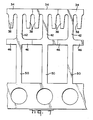
- the state of the art in pin grid arrays has recently developed a requirement for higher density arrays, which results in the two patterns of sockets shown in Figures 3A and 3B.
- the first pattern is a square pattern where the distances between the pins is 0.050 inches.
- the second pattern is known as an "interstitial" pattern where, four pins are provided on a square pattern spaced on 0.100 inch centers and a fifth pin is included centered intermediate every four pins. It is believed that no such socket is commercially available which would accommodate either of the two configurations of aforementioned pin grid arrays.
- the socket 2 of the instant invention includes an insulative housing 4 with a plurality of apertures 6 extending through the housing 4.
- the housing 4 includes an upper face, such as 8, and a lower printed circuit board receiving face 16.
- two designs of sockets are included, the first shown in Figure 3A where the distances "a" and "b” are 0.050 inches and the second embodiment shown in Figure 3B where the distances "c” and “d” are 0.100 inches with a fifth aperture 6 intermediate every four apertures, the second embodiment being called the interstitial configuration.
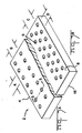
- the socket will be profiled for receiving a pin grid array, such as that shown in Figure 4 as 70, where the pin grid array 70 includes a carrier receiving body, such as 72, having a plurality of pins configured in a dense array as mentioned above.
- the pin grid array 70 further comprises a chip receiving pocket, shown as 74, which receives the leadless chip 80 in a protective manner and serves as a nest in which the chip 80 can be brazed, epoxied, or otherwise attached.
- the plurality of traces, such as 76 are included on the insulative carrier member 72 and are defined in a pattern extending downwardly into the chip receiving pocket for electrical interconnection with the leadless chip.
- the traces 76 extend outwardly from the chip receiving pocket 74 and are electrically interconnected to respective pins 78 of the chip receiving carrier.
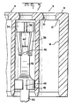
- the insulative housing 4 generally includes an upper carrier receiving face 8 and a lower printed circuit board receiving face 16 with a plurality of pin receiving apertures 6 extending between the two faces. Adjacent the carrier receiving face is a pin receiving diameter 10 which communicates with an inner diameter 14 of the aperture 6. The interface between the pin receiving diameter 10 and the inner diameter 14 defines a downwardly facing shoulder 12.
- each of the terminals generally includes a pin receiving portion 32, a retaining band 46, and a printed circuit board leg, such as 50.
- the pin receiving portion 32 includes a circular band, such as 34, and further includes contact arms, such as 38, extending from the band.
- the terminals are stamped and formed from a flat blank, as shown in Figure 7. Thus, when the blank is rolled to form the circular band 34, a seam 36 is defined.
- Each of the contact arms 38 is inwardly directed towards the center of the circular band portion 34.
- the contact arms 38 are also formed at their ends with radiused portions 40 which form contact points.
- a strap portion 42 extends from the pin receiving portion and the strap portion is inwardly deflected to define a further contact point.
- a second circular band portion 46 is also included as a retention means for the terminal within the aperture 6 and is also stamped from a flat blank and then formed into a circular shape such as that shown in Figure 5.
- the band portion includes a seam, such as 48.
- the cylindrical band portion is not fixedly mounted in the housing and used as a retention feature as in other prior art sockets. Rather, the outer diameter of the cylindrical band portion34 is smaller than the inner diameter 14 of the aperture 6, thus allowing radial expansion of the cylindrical band portion 34. The radial expansion of the cylindrical band portion 34 relieves much of the stress which is created in the contact arms 38 by the insertion of the pins. Furthermore, by having the outer diameter of the circular band portion 34 smaller than the inner diameter 14 of the aperture 6, the pin receiving portion of the terminal can move towards and away from the inner diameter 14 of the aperture 6 accounting for any misalignment of the pins into the pin receiving area.
- the contact arms 38 extend downwardly from the cylindrical band portion 34 and are projected towards the printed circuit board receiving face 16 rather than extending upwardly towards the upper face 8 as in previous socket designs. It should be understood from the discussion relative to Figures 1 and 2 above that a resultant force will occur on the contact arms due to the insertion of the pin and that the resultant force will be normal to the plane on the contact arm. However, since the arms are extending downwardly, the vertical and horizontal components of the force on the contact arms 38 will both create a moment which open the contact arm, thereby reducing insertion force.
- the point of contact between the pins and the contact arms is staggered. As shown in Figure 6, the point of contact 40 for the contact arms 38 is lower than the point of contact 44 for the strap portion 42. As the points of contact are axially offset, the force required to deflect those contact portions occurs in a stepped fashion such that the force required to open all three contact points does not occur simultaneously causing an additive force.
- each of the terminals 30 further comprises a second cylindrical band portion 46 which has an outer diameter which is larger than the inner diameter 14 of the aperture 6.
- the circular band portion 46 becomes a circular spring which will store energy and attempt to radially expand, thereby retaining the terminals 30 within their associated apertures 6.
Abstract
Description
- The subject invention relates to sockets for soldering to printed circuit boards which can accept a pin grid array (PGA) having a plurality of pins.
- U.S. Patent 4,498,725; U.S. Patent 4,648,669; and U.S. Patent 4,679,318 relate generally to sockets for pin grid arrays.
- Both U.S. Patent 4,648,668 and U.S. Patent 4,498,723 relate to a pin grid array socket which is generally known as a zero insertion force socket. Each of those patents receive a pin grid array and a mechanism is included with the socket which moves the pin grid array into registration with the socket contacts and into electrical engagement therewith.
- U.S. Patent 4,679,318 relates to a socket for a pin grid array which is not zero insertion force and the terminals include opposed contact portions which extend upwardly from a strap or bight portion for receiving a pin downwardly therethrough. A shortcoming of this terminal is that the forces to overcome the spreading of the contact arms to accept the pin, referred to as insertion force, are great due to the dynamics resultantly created by the contact configuration.
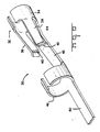
- With reference to Figure 1, the terminal of U.S. Patent 4,679,318 is depicted where, the registration of the terminal with respect to the pin is shown, and the pin is shown poised for receipt within the terminal and in initial contact with the contact arms. At the moment of contact between the pin and the contact arms, a resultant force F is imposed on each of the contact arms normal to the point of contact.
- Referring now to Figure 2 shows that the force imposed on the contact arms includes two components, a vertical component FV and a horizontal component FH. Given that the contact arms will rotate about the interconnection between the contact arms and the strap at a point such as C, the vertical component FV will impose a clockwise moment on the contact arms, with respect to point C, and will attempt to pinch the contact arms closed. Admittedly, the horizontal component FH is larger than the vertical FV and the resultant moment will be counterclockwise about point C, and will open the contact arms and accept the pin. However, the vertical component of the force is doing negative work by attempting to close the contact arms, therefore, the overall force must be increased to achieve a horizontal force large enough to open the contact arms. As the number of pins on the PGAs increases, so will the total insertion force required to insert the PGAs within their associated sockets, which could resultantly damage the PGAs.
- Furthermore, the terminal shown in U.S. Patent 4,679,318 appears to use the strap portion and the side walls for retention of the terminal within the respective apertures, which disallows the expansion of the strap portion.
- Furthermore, the terminals in U.S. Patent 4,679,318 appear to be box-shaped and are not capable for use in a high density array.
- The state of the art in pin grid arrays has a recent requirement for higher density spacing requirements for the pins on the array. It is believed that no such socket terminal is commercially available which can accommodate these increases in pin density.
- Therefore, it is an object of the instant invention to design a terminal for a pin grid array socket which is capable for use in such high density arrays.
- It is a further object of the invention to minimize the insertion force of the pin grid array.
- It is a further object of the invention to include a centering feature of the terminals such that misaligned pins of the pin grid array will align with the pin receiving area of the terminal.
- The objects of the invention were met by defining the socket as an insulating housing having an upper carrier receiving face and a lower printed circuit board receiving face where the housing has a plurality of apertures extending between the two housing faces. A plurality of electrical terminals are disposed within the apertures and include a base portion which includes an integral pin receiving portion for electrical interconnection with the carrier pins and a tail portion which extends beyond the printed circuit board receiving face for electrical connection with the printed circuit board.
- Preferably, the pin receiving portion includes a circular band portion and has resilient contact portions extending therefrom and downwardly into the aperture towards the printed circuit board receiving face.
- Preferably, the circular band portion is profiled smaller than its surrounding through hole which allows the pin receiving portion to find its center.
- Preferably, the band portion has a seam which allows the band portion to expand thereby alleviating some of the stresses in the contact arms.
- The preferred embodiment of the invention will now be described in view of the following figures.
- The preferred embodiment of the invention will now be described in view of the following drawings, where:
- Figure 1 shows the disposition of a terminal and pin of a prior art socket.
- Figure 2 is a diagrammatical view of the resultant force of the pin on the terminal of the prior art.
- Figure 3A shows a first embodiment of the socket of the instant invention.
- Figure 3B shows a second embodiment of the socket of the instant invention.
- Figure 4 shows a conventional pin grid array.
- Figure 5 is a cross-sectional view through lines 5-5 of Figure 4.
- Figure 6 is a side view of the terminal of the instant invention.
- Figure 7 is a top plan view of the stamped blank of the instant invention.
- The state of the art in pin grid arrays has recently developed a requirement for higher density arrays, which results in the two patterns of sockets shown in Figures 3A and 3B. The first pattern is a square pattern where the distances between the pins is 0.050 inches. The second pattern is known as an "interstitial" pattern where, four pins are provided on a square pattern spaced on 0.100 inch centers and a fifth pin is included centered intermediate every four pins. It is believed that no such socket is commercially available which would accommodate either of the two configurations of aforementioned pin grid arrays.
- I have invented a socket, and the terminals therefore, which are capable of accommodating the pin grid arrays which are configured as described above.
- Referring first to Figures 3A and 3B, the
socket 2 of the instant invention includes aninsulative housing 4 with a plurality ofapertures 6 extending through thehousing 4. Thehousing 4 includes an upper face, such as 8, and a lower printed circuitboard receiving face 16. As discussed above, two designs of sockets are included, the first shown in Figure 3A where the distances "a" and "b" are 0.050 inches and the second embodiment shown in Figure 3B where the distances "c" and "d" are 0.100 inches with afifth aperture 6 intermediate every four apertures, the second embodiment being called the interstitial configuration. - In either event, the socket will be profiled for receiving a pin grid array, such as that shown in Figure 4 as 70, where the
pin grid array 70 includes a carrier receiving body, such as 72, having a plurality of pins configured in a dense array as mentioned above. Thepin grid array 70 further comprises a chip receiving pocket, shown as 74, which receives theleadless chip 80 in a protective manner and serves as a nest in which thechip 80 can be brazed, epoxied, or otherwise attached. The plurality of traces, such as 76, are included on theinsulative carrier member 72 and are defined in a pattern extending downwardly into the chip receiving pocket for electrical interconnection with the leadless chip. Thetraces 76 extend outwardly from thechip receiving pocket 74 and are electrically interconnected torespective pins 78 of the chip receiving carrier. - With reference now to Figure 5 which is a cross-sectional view through lines 5-5 of Figure 3A, the
insulative housing 4 generally includes an uppercarrier receiving face 8 and a lower printed circuitboard receiving face 16 with a plurality ofpin receiving apertures 6 extending between the two faces. Adjacent the carrier receiving face is apin receiving diameter 10 which communicates with aninner diameter 14 of theaperture 6. The interface between thepin receiving diameter 10 and theinner diameter 14 defines a downwardly facingshoulder 12. - With reference to Figures 5 and 6, a plurality of terminals are inserted within the
insulative housing 4 within theapertures 6 and each of the terminals generally includes apin receiving portion 32, aretaining band 46, and a printed circuit board leg, such as 50. - The
pin receiving portion 32 includes a circular band, such as 34, and further includes contact arms, such as 38, extending from the band. The terminals are stamped and formed from a flat blank, as shown in Figure 7. Thus, when the blank is rolled to form thecircular band 34, aseam 36 is defined. Each of thecontact arms 38 is inwardly directed towards the center of thecircular band portion 34. Thecontact arms 38 are also formed at their ends withradiused portions 40 which form contact points. As shown in Figure 6, astrap portion 42 extends from the pin receiving portion and the strap portion is inwardly deflected to define a further contact point. A secondcircular band portion 46 is also included as a retention means for the terminal within theaperture 6 and is also stamped from a flat blank and then formed into a circular shape such as that shown in Figure 5. The band portion includes a seam, such as 48. - In an effort to place the terminals in the configuration shown in Figure 1 where the spacing between the terminals is 0.050 inches on a side, the terminals must per se be less than 0.050 inches on the diameter. For this reason, two opposed contact arms cannot be utilized as the width of the arms enlarges the terminal to a profile which cannot fit on the 0.050 inch by 0.050 inch grid. Rather, three contact arms are utilized where each of the contact arms is approximately 120 apart. However, this makes each of the
contact arms 38 so small that the stress at the juncture of the contact arms and thecircular band portion 34 is high enough to plastically deform the contact arms, if the arms are not post heat treated. For this reason, the cylindrical band portion is not fixedly mounted in the housing and used as a retention feature as in other prior art sockets. Rather, the outer diameter of the cylindrical band portion34 is smaller than theinner diameter 14 of theaperture 6, thus allowing radial expansion of thecylindrical band portion 34. The radial expansion of thecylindrical band portion 34 relieves much of the stress which is created in thecontact arms 38 by the insertion of the pins. Furthermore, by having the outer diameter of thecircular band portion 34 smaller than theinner diameter 14 of theaperture 6, the pin receiving portion of the terminal can move towards and away from theinner diameter 14 of theaperture 6 accounting for any misalignment of the pins into the pin receiving area. - Due to the increase in density of the array of pins, the total insertion force must be kept to a minimum. For this reason, the
contact arms 38 extend downwardly from thecylindrical band portion 34 and are projected towards the printed circuitboard receiving face 16 rather than extending upwardly towards theupper face 8 as in previous socket designs. It should be understood from the discussion relative to Figures 1 and 2 above that a resultant force will occur on the contact arms due to the insertion of the pin and that the resultant force will be normal to the plane on the contact arm. However, since the arms are extending downwardly, the vertical and horizontal components of the force on thecontact arms 38 will both create a moment which open the contact arm, thereby reducing insertion force. - To further reduce the insertion force, the point of contact between the pins and the contact arms is staggered. As shown in Figure 6, the point of
contact 40 for thecontact arms 38 is lower than the point ofcontact 44 for thestrap portion 42. As the points of contact are axially offset, the force required to deflect those contact portions occurs in a stepped fashion such that the force required to open all three contact points does not occur simultaneously causing an additive force. - As the outer diameter of the
cylindrical band portion 34 is smaller than theinner diameter 14 of theaperture 6, retention means independent of the pin receiving portion must be provided on the terminals. As shown in Figures 5 and 6, each of theterminals 30 further comprises a secondcylindrical band portion 46 which has an outer diameter which is larger than theinner diameter 14 of theaperture 6. Thus, thecircular band portion 46 becomes a circular spring which will store energy and attempt to radially expand, thereby retaining theterminals 30 within their associatedapertures 6.
Claims (14)
the pin receiving portion (32) including a band portion (34) disposed proximate to the upper carrier receiving face (8) and having resilient contact arms (38) extending therefrom with a free end extending downwardly into the aperture (6), the contact arms (38) converging generally inwardly towards the printed circuit board receiving face.
Applications Claiming Priority (2)
| Application Number | Priority Date | Filing Date | Title |
|---|---|---|---|
| US13230787A | 1987-12-15 | 1987-12-15 | |
| US132307 | 1987-12-15 |
Publications (2)
| Publication Number | Publication Date |
|---|---|
| EP0321212A1 true EP0321212A1 (en) | 1989-06-21 |
| EP0321212B1 EP0321212B1 (en) | 1993-06-02 |
Family
ID=22453418
Family Applications (1)
| Application Number | Title | Priority Date | Filing Date |
|---|---|---|---|
| EP88311829A Expired - Lifetime EP0321212B1 (en) | 1987-12-15 | 1988-12-14 | Socket for pin grid array |
Country Status (4)
| Country | Link |
|---|---|
| EP (1) | EP0321212B1 (en) |
| JP (1) | JPH0766846B2 (en) |
| KR (1) | KR890011145A (en) |
| DE (1) | DE3881493T2 (en) |
Cited By (8)
| Publication number | Priority date | Publication date | Assignee | Title |
|---|---|---|---|---|
| EP0427563A2 (en) * | 1989-11-09 | 1991-05-15 | Advanced Interconnections Corporation | Apparatus and method for installation of multi-pin components on circuit boards |
| WO1995024747A1 (en) * | 1994-03-11 | 1995-09-14 | The Panda Project | Semiconductor chip affording a high-density external interface |
| US5575688A (en) * | 1992-12-01 | 1996-11-19 | Crane, Jr.; Stanford W. | High-density electrical interconnect system |
| US5634821A (en) * | 1992-12-01 | 1997-06-03 | Crane, Jr.; Stanford W. | High-density electrical interconnect system |
| EP0782220A3 (en) * | 1995-12-28 | 1998-08-05 | Berg Electronics Manufacturing B.V. | Electrical connector receptacle with retention means for a plurality of conductive terminals |
| US5812797A (en) * | 1994-03-11 | 1998-09-22 | The Panda Project | Computer having a high density connector system |
| CN103697439A (en) * | 2012-09-27 | 2014-04-02 | 佳駩科技股份有限公司 | Connector of LED lamp tube |
| WO2020018649A1 (en) | 2018-07-17 | 2020-01-23 | Carlisle Interconnect Technologies, Inc. | High speed electrical connector assembly |
Citations (4)
| Publication number | Priority date | Publication date | Assignee | Title |
|---|---|---|---|---|
| GB1087299A (en) * | 1963-10-31 | 1967-10-18 | Plessey Uk Ltd | Improvements in or relating to socket contacts for electrical connectors |
| NL6912744A (en) * | 1969-08-21 | 1971-02-23 | ||
| FR2529023A1 (en) * | 1982-06-17 | 1983-12-23 | Ctm | Female contact for telecommunications jack-plug socket - has staggered spring contacts which provide electrical contact which is not dependent on contact separation distance |
| FR2579834A1 (en) * | 1985-03-27 | 1986-10-03 | Allied Corp | TULIP TYPE CONTACT FOR INTEGRATED CIRCUIT SUPPORT |
Family Cites Families (5)
| Publication number | Priority date | Publication date | Assignee | Title |
|---|---|---|---|---|
| JPS57164210A (en) * | 1981-04-02 | 1982-10-08 | Kurimoto Iron Works Ltd | Apparatus of fluidized layer |
| JPS60136080U (en) * | 1984-02-22 | 1985-09-10 | 日本航空電子工業株式会社 | Rotatable connector |
| JPH0521045Y2 (en) * | 1985-07-01 | 1993-05-31 | ||
| JPH0331022Y2 (en) * | 1985-10-08 | 1991-07-01 | ||
| JPH0332062Y2 (en) * | 1986-03-28 | 1991-07-08 |
-
1988
- 1988-12-12 KR KR1019880016457A patent/KR890011145A/en not_active Application Discontinuation
- 1988-12-14 DE DE88311829T patent/DE3881493T2/en not_active Expired - Fee Related
- 1988-12-14 EP EP88311829A patent/EP0321212B1/en not_active Expired - Lifetime
- 1988-12-15 JP JP63317556A patent/JPH0766846B2/en not_active Expired - Lifetime
Patent Citations (4)
| Publication number | Priority date | Publication date | Assignee | Title |
|---|---|---|---|---|
| GB1087299A (en) * | 1963-10-31 | 1967-10-18 | Plessey Uk Ltd | Improvements in or relating to socket contacts for electrical connectors |
| NL6912744A (en) * | 1969-08-21 | 1971-02-23 | ||
| FR2529023A1 (en) * | 1982-06-17 | 1983-12-23 | Ctm | Female contact for telecommunications jack-plug socket - has staggered spring contacts which provide electrical contact which is not dependent on contact separation distance |
| FR2579834A1 (en) * | 1985-03-27 | 1986-10-03 | Allied Corp | TULIP TYPE CONTACT FOR INTEGRATED CIRCUIT SUPPORT |
Cited By (27)
| Publication number | Priority date | Publication date | Assignee | Title |
|---|---|---|---|---|
| EP0427563A2 (en) * | 1989-11-09 | 1991-05-15 | Advanced Interconnections Corporation | Apparatus and method for installation of multi-pin components on circuit boards |
| EP0427563A3 (en) * | 1989-11-09 | 1991-07-31 | Advanced Interconnections Corporation | Apparatus and method for installation of multi-pin components on circuit boards |
| US5967850A (en) * | 1992-12-01 | 1999-10-19 | Crane, Jr.; Stanford W. | High-density electrical interconnect system |
| US5641309A (en) * | 1992-12-01 | 1997-06-24 | Crane, Jr.; Stanford W. | High-density electrical interconnect system |
| US5575688A (en) * | 1992-12-01 | 1996-11-19 | Crane, Jr.; Stanford W. | High-density electrical interconnect system |
| US5634821A (en) * | 1992-12-01 | 1997-06-03 | Crane, Jr.; Stanford W. | High-density electrical interconnect system |
| US6203347B1 (en) | 1992-12-01 | 2001-03-20 | Silicon Bandwidth Inc. | High-density electrical interconnect system |
| US5951320A (en) * | 1992-12-01 | 1999-09-14 | Crane, Jr.; Stanford W. | Electrical interconnect system with wire receiving portion |
| US6554651B2 (en) | 1992-12-01 | 2003-04-29 | Stanford W. Crane, Jr. | High-density electrical interconnect system |
| US5812797A (en) * | 1994-03-11 | 1998-09-22 | The Panda Project | Computer having a high density connector system |
| US5696027A (en) * | 1994-03-11 | 1997-12-09 | The Panda Project | Method of manufacturing a semiconductor chip carrier affording a high-density external interface |
| WO1995024747A1 (en) * | 1994-03-11 | 1995-09-14 | The Panda Project | Semiconductor chip affording a high-density external interface |
| US6073229A (en) * | 1994-03-11 | 2000-06-06 | The Panda Project | Computer system having a modular architecture |
| US6097086A (en) * | 1994-03-11 | 2000-08-01 | Silicon Bandwidth, Inc. | Semiconductor chip carrier including an interconnect component interface |
| US5541449A (en) * | 1994-03-11 | 1996-07-30 | The Panda Project | Semiconductor chip carrier affording a high-density external interface |
| US5892280A (en) * | 1994-03-11 | 1999-04-06 | Crane, Jr.; Stanford W. | Semiconductor chip carrier affording a high-density external interface |
| US6574726B2 (en) | 1994-03-11 | 2003-06-03 | Silicon Bandwidth, Inc. | Modular architecture for high bandwidth computers |
| US7103753B2 (en) | 1994-03-11 | 2006-09-05 | Silicon Bandwith Inc. | Backplane system having high-density electrical connectors |
| US6577003B1 (en) | 1994-03-11 | 2003-06-10 | Silicon Bandwidth, Inc. | Semiconductor chip carrier affording a high-density external interface |
| US7183646B2 (en) | 1994-03-11 | 2007-02-27 | Silicon Bandwidth, Inc. | Semiconductor chip carrier affording a high-density external interface |
| EP0782220A3 (en) * | 1995-12-28 | 1998-08-05 | Berg Electronics Manufacturing B.V. | Electrical connector receptacle with retention means for a plurality of conductive terminals |
| CN103697439A (en) * | 2012-09-27 | 2014-04-02 | 佳駩科技股份有限公司 | Connector of LED lamp tube |
| EP2713446A1 (en) * | 2012-09-27 | 2014-04-02 | Justing Technology (Taiwan) Pte Ltd. | Connector of a light-emitting-diode lamp tube |
| WO2020018649A1 (en) | 2018-07-17 | 2020-01-23 | Carlisle Interconnect Technologies, Inc. | High speed electrical connector assembly |
| CN112673528A (en) * | 2018-07-17 | 2021-04-16 | 卡莱尔互联科技有限公司 | High speed electrical connector assembly |
| EP3824515A4 (en) * | 2018-07-17 | 2022-04-06 | Carlisle Interconnect Technologies, Inc. | High speed electrical connector assembly |
| CN112673528B (en) * | 2018-07-17 | 2023-10-13 | 卡莱尔互联科技有限公司 | High-speed electric connector assembly |
Also Published As
| Publication number | Publication date |
|---|---|
| JPH0265080A (en) | 1990-03-05 |
| DE3881493T2 (en) | 1994-01-05 |
| KR890011145A (en) | 1989-08-12 |
| DE3881493D1 (en) | 1993-07-08 |
| JPH0766846B2 (en) | 1995-07-19 |
| EP0321212B1 (en) | 1993-06-02 |
Similar Documents
| Publication | Publication Date | Title |
|---|---|---|
| US4934967A (en) | Socket for pin grid array | |
| EP0664581B1 (en) | Low profile board to board connector | |
| EP0349595B1 (en) | Edge connector for circuit boards | |
| EP0392549B1 (en) | Surface mount electrical connector | |
| EP0384580B1 (en) | Surface mount HDI contact | |
| US4842528A (en) | Solder post retention means | |
| EP0411888B1 (en) | Electrical connector | |
| US4708660A (en) | Connector for orthogonally mounting circuit boards | |
| US5085590A (en) | Shielded stackable connector assembly | |
| US5490787A (en) | Electrical connector with integral supporting structure | |
| US3955869A (en) | Electrical socket and socket contact adapted for use therewith | |
| US5411404A (en) | Electrical connector having bus bars providing circuit board retention | |
| US4619495A (en) | High-density press-fit cardedge connectors | |
| EP0340730B1 (en) | Multiple contact assembly for receiving a contact edge of a thin printed circuit card and flexible contact member for this purpose | |
| US3404367A (en) | Disengageable electrical connections | |
| US4722700A (en) | Low insertion force terminal for use with circuit panel | |
| US5558540A (en) | Multi-connector assembly | |
| EP0321212A1 (en) | Socket for pin grid array | |
| US4725250A (en) | High density circuit panel socket | |
| GB2276283A (en) | Electrical connector with short-circuiting facility | |
| US5009606A (en) | Separable electrical connector | |
| US4907978A (en) | Self-retaining connector | |
| US5320549A (en) | Connector with press-fit terminal pins | |
| EP0299989B1 (en) | High density circuit panel socket | |
| US6431878B1 (en) | Socket for PGA package |
Legal Events
| Date | Code | Title | Description |
|---|---|---|---|
| PUAI | Public reference made under article 153(3) epc to a published international application that has entered the european phase |
Free format text: ORIGINAL CODE: 0009012 |
|
| AK | Designated contracting states |
Kind code of ref document: A1 Designated state(s): DE FR GB IT NL |
|
| RAP3 | Party data changed (applicant data changed or rights of an application transferred) |
Owner name: AMP INCORPORATED (A NEW JERSEY CORPORATION) |
|
| RAP1 | Party data changed (applicant data changed or rights of an application transferred) |
Owner name: AMP INCORPORATED |
|
| 17P | Request for examination filed |
Effective date: 19891201 |
|
| 17Q | First examination report despatched |
Effective date: 19920214 |
|
| RAP1 | Party data changed (applicant data changed or rights of an application transferred) |
Owner name: THE WHITAKER CORPORATION |
|
| GRAA | (expected) grant |
Free format text: ORIGINAL CODE: 0009210 |
|
| ITF | It: translation for a ep patent filed |
Owner name: BARZANO' E ZANARDO MILANO S.P.A. |
|
| AK | Designated contracting states |
Kind code of ref document: B1 Designated state(s): DE FR GB IT NL |
|
| REF | Corresponds to: |
Ref document number: 3881493 Country of ref document: DE Date of ref document: 19930708 |
|
| ET | Fr: translation filed | ||
| PLBE | No opposition filed within time limit |
Free format text: ORIGINAL CODE: 0009261 |
|
| STAA | Information on the status of an ep patent application or granted ep patent |
Free format text: STATUS: NO OPPOSITION FILED WITHIN TIME LIMIT |
|
| 26N | No opposition filed | ||
| PGFP | Annual fee paid to national office [announced via postgrant information from national office to epo] |
Ref country code: GB Payment date: 19961108 Year of fee payment: 9 |
|
| PGFP | Annual fee paid to national office [announced via postgrant information from national office to epo] |
Ref country code: FR Payment date: 19961211 Year of fee payment: 9 |
|
| PGFP | Annual fee paid to national office [announced via postgrant information from national office to epo] |
Ref country code: DE Payment date: 19961227 Year of fee payment: 9 |
|
| PG25 | Lapsed in a contracting state [announced via postgrant information from national office to epo] |
Ref country code: GB Free format text: LAPSE BECAUSE OF NON-PAYMENT OF DUE FEES Effective date: 19971214 |
|
| PG25 | Lapsed in a contracting state [announced via postgrant information from national office to epo] |
Ref country code: FR Free format text: THE PATENT HAS BEEN ANNULLED BY A DECISION OF A NATIONAL AUTHORITY Effective date: 19971231 |
|
| GBPC | Gb: european patent ceased through non-payment of renewal fee |
Effective date: 19971214 |
|
| PG25 | Lapsed in a contracting state [announced via postgrant information from national office to epo] |
Ref country code: DE Free format text: LAPSE BECAUSE OF NON-PAYMENT OF DUE FEES Effective date: 19980901 |
|
| PGFP | Annual fee paid to national office [announced via postgrant information from national office to epo] |
Ref country code: NL Payment date: 19980914 Year of fee payment: 11 |
|
| REG | Reference to a national code |
Ref country code: FR Ref legal event code: ST |
|
| PG25 | Lapsed in a contracting state [announced via postgrant information from national office to epo] |
Ref country code: NL Free format text: LAPSE BECAUSE OF NON-PAYMENT OF DUE FEES Effective date: 20000701 |
|
| NLV4 | Nl: lapsed or anulled due to non-payment of the annual fee |
Effective date: 20000701 |
|
| PG25 | Lapsed in a contracting state [announced via postgrant information from national office to epo] |
Ref country code: IT Free format text: LAPSE BECAUSE OF NON-PAYMENT OF DUE FEES;WARNING: LAPSES OF ITALIAN PATENTS WITH EFFECTIVE DATE BEFORE 2007 MAY HAVE OCCURRED AT ANY TIME BEFORE 2007. THE CORRECT EFFECTIVE DATE MAY BE DIFFERENT FROM THE ONE RECORDED. Effective date: 20051214 |