EP0323226A2 - An image forming apparatus - Google Patents
An image forming apparatus Download PDFInfo
- Publication number
- EP0323226A2 EP0323226A2 EP88312361A EP88312361A EP0323226A2 EP 0323226 A2 EP0323226 A2 EP 0323226A2 EP 88312361 A EP88312361 A EP 88312361A EP 88312361 A EP88312361 A EP 88312361A EP 0323226 A2 EP0323226 A2 EP 0323226A2
- Authority
- EP
- European Patent Office
- Prior art keywords
- image
- transfer
- bearing member
- voltage
- image bearing
- Prior art date
- Legal status (The legal status is an assumption and is not a legal conclusion. Google has not performed a legal analysis and makes no representation as to the accuracy of the status listed.)
- Granted
Links
Images


Classifications
-
- H—ELECTRICITY
- H03—ELECTRONIC CIRCUITRY
- H03H—IMPEDANCE NETWORKS, e.g. RESONANT CIRCUITS; RESONATORS
- H03H15/00—Transversal filters
-
- G—PHYSICS
- G03—PHOTOGRAPHY; CINEMATOGRAPHY; ANALOGOUS TECHNIQUES USING WAVES OTHER THAN OPTICAL WAVES; ELECTROGRAPHY; HOLOGRAPHY
- G03G—ELECTROGRAPHY; ELECTROPHOTOGRAPHY; MAGNETOGRAPHY
- G03G15/00—Apparatus for electrographic processes using a charge pattern
- G03G15/14—Apparatus for electrographic processes using a charge pattern for transferring a pattern to a second base
- G03G15/16—Apparatus for electrographic processes using a charge pattern for transferring a pattern to a second base of a toner pattern, e.g. a powder pattern, e.g. magnetic transfer
- G03G15/1665—Apparatus for electrographic processes using a charge pattern for transferring a pattern to a second base of a toner pattern, e.g. a powder pattern, e.g. magnetic transfer by introducing the second base in the nip formed by the recording member and at least one transfer member, e.g. in combination with bias or heat
- G03G15/167—Apparatus for electrographic processes using a charge pattern for transferring a pattern to a second base of a toner pattern, e.g. a powder pattern, e.g. magnetic transfer by introducing the second base in the nip formed by the recording member and at least one transfer member, e.g. in combination with bias or heat at least one of the recording member or the transfer member being rotatable during the transfer
- G03G15/1675—Apparatus for electrographic processes using a charge pattern for transferring a pattern to a second base of a toner pattern, e.g. a powder pattern, e.g. magnetic transfer by introducing the second base in the nip formed by the recording member and at least one transfer member, e.g. in combination with bias or heat at least one of the recording member or the transfer member being rotatable during the transfer with means for controlling the bias applied in the transfer nip
-
- G—PHYSICS
- G03—PHOTOGRAPHY; CINEMATOGRAPHY; ANALOGOUS TECHNIQUES USING WAVES OTHER THAN OPTICAL WAVES; ELECTROGRAPHY; HOLOGRAPHY
- G03G—ELECTROGRAPHY; ELECTROPHOTOGRAPHY; MAGNETOGRAPHY
- G03G15/00—Apparatus for electrographic processes using a charge pattern
-
- G—PHYSICS
- G03—PHOTOGRAPHY; CINEMATOGRAPHY; ANALOGOUS TECHNIQUES USING WAVES OTHER THAN OPTICAL WAVES; ELECTROGRAPHY; HOLOGRAPHY
- G03G—ELECTROGRAPHY; ELECTROPHOTOGRAPHY; MAGNETOGRAPHY
- G03G15/00—Apparatus for electrographic processes using a charge pattern
- G03G15/02—Apparatus for electrographic processes using a charge pattern for laying down a uniform charge, e.g. for sensitising; Corona discharge devices
- G03G15/0208—Apparatus for electrographic processes using a charge pattern for laying down a uniform charge, e.g. for sensitising; Corona discharge devices by contact, friction or induction, e.g. liquid charging apparatus
- G03G15/0216—Apparatus for electrographic processes using a charge pattern for laying down a uniform charge, e.g. for sensitising; Corona discharge devices by contact, friction or induction, e.g. liquid charging apparatus by bringing a charging member into contact with the member to be charged, e.g. roller, brush chargers
- G03G15/0225—Apparatus for electrographic processes using a charge pattern for laying down a uniform charge, e.g. for sensitising; Corona discharge devices by contact, friction or induction, e.g. liquid charging apparatus by bringing a charging member into contact with the member to be charged, e.g. roller, brush chargers provided with means for cleaning the charging member
-
- G—PHYSICS
- G03—PHOTOGRAPHY; CINEMATOGRAPHY; ANALOGOUS TECHNIQUES USING WAVES OTHER THAN OPTICAL WAVES; ELECTROGRAPHY; HOLOGRAPHY
- G03G—ELECTROGRAPHY; ELECTROPHOTOGRAPHY; MAGNETOGRAPHY
- G03G2215/00—Apparatus for electrophotographic processes
- G03G2215/02—Arrangements for laying down a uniform charge
- G03G2215/021—Arrangements for laying down a uniform charge by contact, friction or induction
Definitions
- the present invention relates to an image forming apparatus using an electrostatic image transfer process such as an electrostatic copying machine or printer, more particularly to such an image forming apparatus provided with a charging electrode for charging an image bearing member.
- An image forming apparatus wherein a surface of a photosensitive layer of an image bearing member in the form of a rotatable cylinder is electrically charged by a corona charging device; an electrostatic latent image is formed thereon; the electrostatic latent image is developed; and the developed image is transferred by passing a transfer material (a sheet of paper) through a nip formed between the image bearing member and a transfer drum or roller (charging electrode) press-contacted to the image bearing member, wherein a transfer bias is applied to the transfer roller to transfer the transferable developed (toner) image from the image bearing member surface to the transfer material or sheet.
- a transfer material a sheet of paper
- a transfer drum or roller charging electrode
- Such an apparatus involves a problem that the transfer roller is significantly contaminated when the image of the original is larger than the size of the transfer material so that the toner is directly transferred from the image bearing member to the transfer roller or when jam occurs during image forming operation. If the contamination of the roller takes place, the subsequent transfer material is contaminated, or the transfer bias is substantially decreased with the result that the image transfer becomes insufficient.
- the electric field for transferring the toner from the transfer roller to the image bearing member can be insufficient, only by applying the bias voltage having the opposite polarity (the same polarity as the toner) during the non-transfer operation, described above. Therefore, the transfer roller is not sufficiently cleaned.
- a printer of an electrophotographic type using a laser beam or LED elements becomes widely used because computers are widely used. In the printer like this, in order to minimize the light emitting period of the light source to increase the service life, it is frequent that the light is projected to such an area as is going to become an image portion (not background portion) after development, and therefore, the latent image is reverse-developed.
- the polarity of the electrically charged image bearing member and the polarity of the bias voltage applied to the transfer roller for the cleaning are the same, unlike the case of regular development, during non-transfer operation (no sheet between the roller and the image bearing member), and therefore, sufficient electrostatic contrast for the cleaning is not provided.
- the image forming apparatus comprises a photosensitive member 1 extending in a direction perpendicular to the sheet of the drawing and rotatable in a direction indicated by an arrow A.
- the surface of the photosensitive member 1 is uniformly charged by a corona charger 2, and thereafter, light is projected thereonto in accordance with an image signal, so that an electrostatic latent image is formed.
- a developing device 4 the latent image is visualized with the toner.
- a transfer material 10 reaches the nip N because it is supplied thereto through a conveyance passage 5 with timed relation with the latent image. Then, a transfer bias is applied to the transfer roller 6 from a power source 7, so that the toner image is transferred onto the transfer material. Referring back to the charger 2, it is supplied with a voltage for charging the photosensitive member (image bearing member) 1 from the power source 11, whereas a developing sleeve 4A of the developing device 4 is supplied with a developing bias voltage from a power source 12.
- the transfer material discharged from the nip N is further advanced in the leftward direction to an unshown image fixing station, where the unfixed toner image on the transfer material 10 is fixed thereon.
- the toner on the photosensitive member 1 which is not transferred to the transfer material during the transfer operation reaches with rotation of the photosensitive member to a cleaning device 8 where remaining toner is removed from the photosensitive member.
- the electric charge remaining on the surface of the photosensitive member is erased by illumination by a discharging lamp 9, so that the photosensitive member 1 is prepared for the next image forming operation.
- the image forming apparatus shown in the Figure is a laser beam printer of an electrophotographic type.
- the latent image formation and image transfer therein will be described.
- the photosensitive member 1 is provided with an organic photoconductor (OPC) layer and is charged to -700 V by the corona charger 2 and is exposed by a laser scanning device 3 to a laser beam modulated in accordance with an image signal by a controller 13.
- OPC organic photoconductor
- Such an area of the photosensitive member 1 as will become an image portion (characters or the like) after development is exposed to the laser beam.
- the image portion potential attenuates to -100 V, so that a latent image is formed.
- the toner having been charged to the same polarity as the charge applied to the photosensitive member 1 by the corona charger 2, that is, negatively charged toner is supplied thereto, whereby the toner is deposited to such an area where the potential is attenuated by the application of the laser beam, so that a toner image is formed. That is, the latent image is reverse-developed.
- the toner image now formed on the photosensitive member 1 reaches, with rotation of the photosensitive member 1, to the nip N, where a transfer material 10 supplied through the conveyance passage 5 is contacted to the photosensitive member 1, so that the transfer material 10, the photosensitive member 1 and the transfer roller are advanced at the same speed.
- the transfer roller 6 is supplied with a transfer bias of +500 V (the polarity opposite to the charge of the toner) from the power source 7, by which an image transfer electric field is formed, so that the toner image is transferred from the photosensitive member 1 to the transfer material 10.
- the material of the photosensitive member 1 described above is not limiting, but may be amorphous silicon, selenium, ZnO or the like.
- the power source 11 for the corona charger 2, the laser exposure device 3, the power source 12 for the developing sleeve 4A and the power source 7 for the transfer roller 6 are on-off controlled by the controller 13.
- a non-image formation area an area which is to correspond to non-passage of the transfer material when it reaches to the transfer station, or an area which is to correspond to non-exposure period of the photosensitive member to the light information
- the charger 2 is not energized, whereby the surface potential of the photosensitive member 1 in such an area is 0 V.
- the developing bias applied to the developing sleeve is not supplied, or otherwise, the developing bias is switched to a positive polarity, to prevent deposition of the toner to the photosensitive member 1.
- the quantity of laser output varies in dependence on the temperature and humidity.
- the laser beam is continuously produced, and the amount of light is detected, during non-image formation period (between adjacent printing periods in the case of continuous printing, or pre-rotation period in the case of one print) to maintain a constant quantity of light. If the photosensitive member 1 is charged when supplied with the laser beam application for the constant quantity maintenance of the laser beam light, the potential of the portion exposed to the laser beam attenuates, and therefore, two surface potential portions, i.e., -700 V and -100 V are produced.
- the surface potential of the photosensitive member is zero, and therefore, the bias voltage prenventing the toner deposition can be selected form a wide range.
- the developing bias for the non-image formation area can be selected from a range of several hundreds volts when the surface potential of the photosensitive member is near 0 V, from the standpoint of prevention of deposition of the developer to the photosensitive member.
- the developing bias for preventing toner deposition to the photosensitive member can be selected from wide variations including the weakening only of the peak-to-peak voltage of the AC voltage component for the non-image formation area, the shutting-off thereof for the non-image formation area, the changing of the DC component for the non-image formation area, or shutting-off both of them.
- the photosensitive member 1 When the non-image formation area of the photosensitive member 1 is in the image transfer region where the photosensitive member 1 and the transfer roller 6 are press-contacted, that is, during the non-transfer operation, further in other words, when the transfer material is not passed through the transfer region, the photosensitive member 1 is directly contacted to the transfer roller 6, which supplied with a bias voltage of the same polarity as the toner, for example, -500 V to drive the negative toner from the transfer roller 6 to the photosensitive member 1.
- the absolute value of the surface potential of the photosensitive member 1 during the non-passage of the transfer material is smaller than the absolute value of the bias voltage applied to the transfer roller 6.
- the surface potential of the photosensitive member 1 is 0 V, for example, an electric field sufficient for transferring the toner from the transfer roller 6 to the photosensitive member 1 is formed with a relatively low voltage, so that the transfer roller 6 is satisfactorily cleaned.
- FIG. 2 there is shown a timing chart illustrating an operation of the apparatus according to this embodiment, wherein reference A indicates a surface potential of the photosensitive member 1, and the pulse-like portion in the image area indicates a potential pattern provided by the information light application.
- Reference character B indicates switching of the developing bias.
- the non-charged portion is to receive the toner, and therefore, in this embodiment, the switching of the bias voltage is to overlap with the non-passage of the transfer material through the nip between the photosensitive member 1 and the transfer roller 6, that is, the non-image non-charge area.
- Reference character C designates timing of the switching of the bias voltage to the transfer roller.
- the bias voltage is positive when the transfer roller 6 is opposed to the image area of the photosensitive member 1 (during passage of the transfer material), and is negative when the transfer roller 6 is opposed to the non-image area (during the transfer material is not passed).
- the developing bias is switched so as to be overlapped with the non-charge portion from the standpoint of deposition of the toner to the photosensitive member 1. Adjacent starting and terminating points of time, the developing bias voltage becomes 0 V under the condition that the surface potential of the photosensitive member is -700 V, and therefore, the normally charged (negative in this case) toner is prevented from deposition.
- a reversely charged toner (positive charged in this case) in the one component developer or the carrier particles positively charged in the two component developer can be deposited to the photosensitive member in the developing device, because a strong reverse electric field is formed for a short period of time.
- the reversely charged toner and/or the carrier can be transferred back to the transfer roller 6 and can contaminate it. Therefore, it is preferable that the polarity of the bias to the transfer roller is switched to the same as the normal toner, when the no-charge portion is opposed to the transfer roller, since their the reversely charged toner or the like is not deposited to the photosensitive member.
- the charger is stopped at the non-image formation area of the photosensitive member 1 (the area of the photosensitive member opposed to the transfer roller when the transfer material is not passed through the nip), but, the charging voltage of the charger may be made smaller than for the image area, or alternatively, a bias voltage for a grid, if it is provided for the corona charger, or may be controlled to decrease the potential of the non-image formation area of the photosensitive member 1.
- the non-image formation area of the photosensitive member 1 is once charged by the charger to the same extent as the image formation area, and thereafter, the charge in the non-image formation area of the photosensitive member may be removed or decreased.
- the potential may be decreased by applying light to the non-image region of the photosensitive member which has once been charged.
- the potential of the non-image formation area of the photosensitive member is not limited to be 0 V. However, it will suffice if the absolute value of the surface potential of the photosensitive member corresponding to the non-passage of the transfer material is smaller than the absolute value of the bias voltage applied to the transfer roller, when the transfer roller is cleaned.
- a high bias voltage is required to be applied to the transfer roller in order to provide a sufficient potential contrast for satisfactorily cleaning the transfer roller.
- the bias voltage to the transfer roller is required to be -1200 V, in order to form an electric field to transfer the toner from the transfer roller 6 to the photosensitive member 1 by application of a negative (the same as the polarity of the toner) bias voltage to the transfer roller 6.
- the power source device becomes bulky, or another problem of leakage of high voltage results.
- the embodiment of the present invention decreases the potential of the region of the photosensitive member to be opposed or contacted to the transfer roller during non-passage of the transfer material at the transfer station. Further preferably, the potential thereof is 0 V, since then the voltage applied to the transfer roller 6 is small, and the possibility of dielectric break-down of the photosensitive member is reduced, and leakage of current can be prevented. This is particularly effective when the photosensitive member (image bearing member) is of amorphous silicon, OPC or the like having a relatively low durability to the dielectric breakdown.
- FIG. 3 there is shown an image forming apparatus according to another embodiment of the present invention, wherein in place of the corona charger 2 of Figure 1, a charging roller 14 is employed which is made of a conductive rubber and is connected with a source 15 and which is contacted to the photosensitive member 1.
- the charging roller 14 constitutes a contact type charging device to uniformly charge the surface of the photosensitive member 1.
- the charging roller 14 is electrically conductive at least a surface thereof, and the resistance is preferably 102 - 108 ohm.cm, more particularly, it is a roller of electrically conductive urethane rubber having a resistance of 105 ohm.cm in this embodiment.
- the charging roller 14 is supplied from a power source 15 with a vibratory voltage provided by superimposing a DC voltage of -700 V and an AC voltage having a peak-to-peak voltage of 1500 V and a frequency of 1000 Hz, by which the photosensitive layer of the surface of the photosensitive member 1 can be uniformly charged to -700 V.
- the vibratory voltage means a voltage in which the level of the voltage periodically changes with time, and the waveform thereof may be triangular, rectangular or pulse-like.
- a light image is applied to the surface thus charged so that a latent image is formed, and the latent image is reverse-developed so that negatively charged toner particles are deposited to such an area of the latent image as is exposed to the light and is decreased in the potential, whereby a toner image is formed.
- a transfer material 10 is supplied to the photosensitive member in alignment with the toner image.
- the transfer roller 6 is supplied with a DC bias voltage of +500 V, by which a good transferred image can be provided on the transfer material 10.
- the transfer roller 6 is supplied with -500 V.
- the DC component of the voltage applied to the charging roller 16 is shut-off, so that only an AC component is applied, by which the surface of the photosensitive member is uniformly electrically discharged to 0 V.
- the voltage applied to the charging roller may be constituted only with a DC voltage.
- a DC voltage of -1200 - -1300 V is required, and in addition, the uniformness of the surface potential is slightly poorer than when a superposed AC and DC voltage is used with the result that production of a ghost image can not be avoided without provision of the pre-exposure lamp. Therefore, better results can be provided when the superposed voltage is applied to the charging roller 14 than when only a DC voltage is applied.
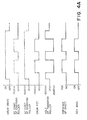
- Figure 4A shows a sequential operation of application of the voltage during charging, developing and image transferring operations.
- the time lag resulting from movement of the photosensitive member is omitted.
- the application of the voltage of -700 V for the DC component to the charging roller 14 is simultaneously with initiation of application of the voltage of 500 V to the transfer roller.
- the DC component to the charging roller 14 is made 0 V, by which the surface potential of the photosensitive member 1 is made 0 V, and also, the bias voltage to the transfer roller 6 is made -500 V, by which the negatively charged toner can be assuredly transferred to the photosensitive member.
- the developing bias is made zero, since then the toner is not transferred without charging.
- the potentials of the charging roller 14 and the transfer roller 6 may be controlled only during the pre-rotation period or post-rotation period, as shown in Figure 4B. Without changing the potentials of the rollers during the non-passage of the transfer material between adjacent transfer material passages in the continuous image forming operation, thus performing no cleaning of the transfer roller, a good image can be provided. It is possible that the cleaning of the transfer roller in the manner described above is performed during a part of the non-passage period.
- the voltage source for applying bias voltage to the transfer roller 6 may be common with the power source for applying a voltage to the charging device, and the intended performance can be provided by a relatively low voltage source, whereby the size of the apparatus can be reduced.
- FIG. 5A there is shown an example of a structure of the power source 15.
- a switch SW1 of a driver circuit K2 When actuated, a voltage of -700 V is produced through a transformer T2 and a rectifier SE2, and a voltage of +1000 V is produced through a rectifier SE3.
- a driver circuit K1 always produces an alternating voltage whenever the photosensitive member is driven, and a voltage of 1500 V (peak-to-peak voltage) is produced through a transformer T1, and a voltage of -500 V is produced by a rectifier SE1.
- the switch SW1 is rendered off, by which only an AC voltage of peak-to-peak voltage of 1500 V is applied to the charging roller 14, and -500 V is applied to the transfer roller 6, whereby the negatively charged toner is returned to the photosensitive member 1.
- FIG. 5B shows another example of the power source, wherein references D1, D2 and D3 designate diodes; C1, C2 and C3 capacitors; and R1 and R7 registers.
- the driving circuit K3 always produces an alternating voltage whenever the photosensitive member 1 is driven.
- the charging roller 14 is supplied through a transformer T3 with a superposed voltage of an AC voltage having a peak-to-peak voltage of 1500 V and a DC voltage of -700 V produced by a rectifier SE4. By closing the switch SW2, it is supplied only with a DC voltage of 1500 V.
- the transfer roller 6 is supplied with +500 V, while by closing the switch SW3, it is supplied with -500 V.
- the DC component of the charging roller 14 is rendered 0 V during the cleaning operation of the transfer roller 6, it may be, as described hereinbefore, made higher than the voltage (-500 V in the examples) applied to the transfer roller 6, for example, it may be made -100 V.
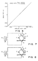
- Figure 6 is a graph showing change of the surface potential of the photosensitive member 1 relative to change of the DC component of the voltage applied to the charging roller 14 with the AC component being fixed to be 1500 V of the peak-to-peak voltage and 1000 Hz of the frequency.
- the surface potential can be freely changed so that the DC component and the surface potential of the photosensitive member can be made equivalent so as to sufficiently clean the transfer roller 6, and therefore, the charging roller 14 is very advantageous over the corona charger 2.
- Figures 7 and 8 show further embodiments.
- the means for uniformly charging the photosensitive member is a blade 16 made of conductive rubber.
- it is a conductive brush 17. Both of them are in sliding contact with the photosensitive member 1.
- the image forming operation and the image transfer operation are repeated. Also as mentioned hereinbefore, when the image forming operation is resumed after temporary stop of the apparatus due to jam occurrence or the like, the toner deposited on the portion of the photosensitive member where the toner image has been formed by the developing device 4 prior to the stoppage and where the toner image has not yet been transferred is directly contacted to the transfer roller 6 at the initial stage of the resumption, and therefore, the toner is directly transferred onto the transfer roller 6.
- warming up time period is provided when the power supply is resumed after interruption of the power supply due to jam occurrence or the like, and that an electric field for transferring the toner from the transfer roller 6 to the photosensitive member, by which the transfer roller 6 is cleaned.
- the transfer roller 6 is supplied with -500 V having a polarity which is the same as that of the negatively charged toner, and the operations of the charger 2 and the developing device 4 are stopped, whereas only the discharging lamp 9 is operated, so that the surface potential of the photosensitive member 1 is attenuated down to 0 V.
- Such an warming up period is continued at least during a period from a point of time when a certain point on the photosensitive member 1 is at the developing device 4 to the point of time when it reaches the nip N between the transfer roller 6 and the photosensitive member 1.
- the warming up period is selected as to be not less than 3 seconds, and after the warming up period, the apparatus is placed in a stand-by period in which the image forming operation is possible.
- the toner image formed between the developing station and the transfer station is not transferred to the transfer roller 6, and is passed through the transfer station as it is to reach the cleaning device, and is removed thereby, and therefore, it can be avoided that such toner is deposited to the transfer roller 6 and contaminates the subsequent transfer material.
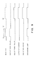
- Figure 9 is a timing chart showing an example of such an image forming apparatus.
- the diameter of the transfer roller 6 is 30 mm, and the peripheral speed is the same as that of the photosensitive member, the warming-up period is not less than 5 seconds.
- the photosensitive member 1 is negatively charged, and the latent image is reverse-developed with negatively charged toner, but the same concept is applicable to the case where the latent image is regularly developed.
- the photosensitive member is charged to -700 V, and the laser scanning device 3 applies light modulated in accordance with an image signal to project light to the white area, by which a latent image is formed on the photosensitive member, and the latent image is regularly charged by positively charged toner with a DC developing bias of -300 V.
- the transfer roller is supplied with a transfer bias voltage of -1500 V, so as to transfer the toner image from the photosensitive member 1 to the transfer material 10.
- a bias voltage having the same polarity as the positively charged toner is applied to the transfer roller 6 during the non-transfer operation, and the region of the photosensitive member 1 which is opposed to the transfer roller 6 during the non-transfer operation is made to have a voltage of approximately 0 V by controlling the charger 2. Because it is about 0 V, it is not developed by the positively charged toner.
- the transfer roller 6, in effect applies to the photosensitive member 1 the electric charge having the polarity opposite to the charge polarity (negative) for charging the photosensitive member 1 by the charger 2.
- the bias voltage to the transfer roller 6 during the non-transfer operation is preferably 0 V ( Figure 12) or has a polarity opposite to that of the toner.
- the region of the photosensitive member 1 which is to be opposed to the transfer roller 6 during the non-transfer operation is charged by the charger 2 to such a level as is higher than the charging level during the image formation, for example, -900 V and on the other hand, the developing bias of the developing device 4 is made near -900 V.
- Figure 10A shows a transfer roller 6 which comprises a metal core 6c, and inside layer 6b made of conductive urethane sponge and an outside layer of solid urethane rubber having electrical conductivity.
- Figure 11 shows change of the cleaning efficiency relative to the contact pressure between such a transfer roller 6 and the photosensitive member 1.
- the transfer efficiency is defined by a percentage of the amount of the toner transferred to the photosensitive member 1 when the transfer roller 6 having toner particles deposited thereon is rotated through three full turns.
- the cleaning efficiency is significantly improved when the contact pressure is not more than 300 g/cm2.
- the nip width of 2 mm could be provided, and the image transfer properties and the sheet conveying properties were without problem, and the cleaning of the transfer roller 6 was so good that the backside of the transfer material was not contaminated. If the contact pressure was decreased, the nip width was decreased, and therefore, the image transfer became insufficient, and the image can be blurred. In view of this, it is preferable that the hardness (JIS (Japanese Industrial Standard) A) of the transfer roller 6 is not more than 30 degrees.
- the roller is of a two layer structure wherein the outside layer surface is made smooth, and the hardness thereof is slightly larger so as to prevent the toner from wedging into the roller surface and so as to increase the durability of the roller, whereas the hardness of the inside layer is made lower to provide the entire hardness in the preferable range.
- the measurement of the roller hardness was performed in accordance with JIS K-6301 using a JIS-A hardness measuring device (TECLOCK GS-706 available from TECLOCK).
- Figures 10B and 10C show another examples of transfer rollers 6.
- it is made of a sponge-like conductive urethane rubber 10d having fine pores with pore diameter of approximately 10 microns.
- Figure 10C it is made of a conductive rubber having plural cavities therein. With those rollers, the same effects can be provided as the transfer roller 6 shown in Figure 10A.
- a surface roughness of the transfer roller 6 is not more than the average particle size of the used toner particles, usually not more than 10 microns, the surface roughness being determined on the basis of ten point average method, since then the image transfer efficiency is improved.
- An example of such a transfer roller 6 can be made by adding a foaming agent into urethane which is made electrically conductive by dispersing and mixing thereinto carbon, and it is foamed in a hollow cylindrical metal mold. By doing so, the surface of the produced roller follows the inside surface of the metal mold to become a skin layer having a surface roughness not more than 10 microns (ten point average measurement), and the roller is electrically conductive.
- the measurement of the surface roughness of the transfer roller 6 is performed in accordance with JIS-B-0601 using a surface configuration measuring device SE-3C available from Kosaka Laboratories, Japan.
- the transfer roller was produced, having a core metal having a diameter of 6 mm, wrapped with foamed urethane having a conductivity of 102 ohm.cm (volume resistivity) and having a thickness of 5 mm.
- the transfer roller thus had a diameter of 16 mm.
- the transfer roller 6 was produced in the manner described above, the surface thereof was abraded to provide the surface roughness Rz of 2s (A) and 10s (B).
- the roller was press-contacted to an OPC photosensitive drum having a diameter of 30 mm with a total pressure of 600 g, wherein the press-contacted area therebetween was 21 cm x 0.1 cm.
- a latent image having a dark potential of -700 V and light potential of -100 V was formed and was developed reversely with negative toner particles having an average particle size of 12 microns.
- the transfer roller was supplied with +500 V.
- the transfer roller was cleaned in the manner described above, the transfer efficiency did not decrease even after several hundreds sheets were processed.
- the surface of the roller after the test was almost the same as prior to the test.
- the transfer roller described above was the one press-contacted to the photosensitive member. However, it is possible to provide a small clearance depending on the thickness of the transfer material, between the transfer roller surface and the photosensitive member surface so that during the transfer operation (passage of the transfer material) the transfer roller press-contact the transfer material to the photosensitive member, whereas during the non-transfer operation, the toner deposited on the transfer roller is transferred to the photosensitive member through the small clearance.
- the image bearing member it is not limited to the photosensitive member, but it is possible to use an insulating drum.
- the transfer means is not limited to the transfer roller, but it may be in the form of an endless belt.
- the application of the present invention is not limited to the cleaning of the transfer means, but is applicable to charging means for charging the image bearing member, for example, the charging roller 14 described above.
- an electric field effective to transfer the toner from the charging electrode to the image bearing member, and the transfer means can be effectively cleaned, by which a good quality of the image can be provided.
Abstract
Description
- The present invention relates to an image forming apparatus using an electrostatic image transfer process such as an electrostatic copying machine or printer, more particularly to such an image forming apparatus provided with a charging electrode for charging an image bearing member.
- An image forming apparatus is known wherein a surface of a photosensitive layer of an image bearing member in the form of a rotatable cylinder is electrically charged by a corona charging device; an electrostatic latent image is formed thereon; the electrostatic latent image is developed; and the developed image is transferred by passing a transfer material (a sheet of paper) through a nip formed between the image bearing member and a transfer drum or roller (charging electrode) press-contacted to the image bearing member, wherein a transfer bias is applied to the transfer roller to transfer the transferable developed (toner) image from the image bearing member surface to the transfer material or sheet.
- Such an apparatus involves a problem that the transfer roller is significantly contaminated when the image of the original is larger than the size of the transfer material so that the toner is directly transferred from the image bearing member to the transfer roller or when jam occurs during image forming operation. If the contamination of the roller takes place, the subsequent transfer material is contaminated, or the transfer bias is substantially decreased with the result that the image transfer becomes insufficient.
- In order to avoid the problem, a proposal has already been made that the transfer roller is supplied, during non-transfer operation, with a bias voltage having a polarity opposite to that during the image transfer operation, by which the toner is intentionally transferred to the image bearing member, thus cleaning the transfer roller, as disclosed in Japanese Laid-Open Patent Application Publication 63837/1979 and Japanese Laid-Open Patent Application No 123577/1981, for example.
- However, the electric field for transferring the toner from the transfer roller to the image bearing member can be insufficient, only by applying the bias voltage having the opposite polarity (the same polarity as the toner) during the non-transfer operation, described above. Therefore, the transfer roller is not sufficiently cleaned. Recently, a printer of an electrophotographic type using a laser beam or LED elements becomes widely used because computers are widely used. In the printer like this, in order to minimize the light emitting period of the light source to increase the service life, it is frequent that the light is projected to such an area as is going to become an image portion (not background portion) after development, and therefore, the latent image is reverse-developed. When the reverse-development type is used, the polarity of the electrically charged image bearing member and the polarity of the bias voltage applied to the transfer roller for the cleaning are the same, unlike the case of regular development, during non-transfer operation (no sheet between the roller and the image bearing member), and therefore, sufficient electrostatic contrast for the cleaning is not provided.
- Accordingly, it is a principal object of the present invention to provide an image forming apparatus wherein toner particles deposited on a charging electrode is transferred to an image bearing member, thus cleaning the charging electrode.
- It is another object of the present invention to provide an image forming apparatus wherein contamination toner particles are removed from a charging electrode, whereby good quality image is stably provided.
- These and other objects, features and advantages of the present invention will become more apparent upon a consideration of the following description of the preferred embodiments of the present invention taken in conjunction with the accompanying drawings.
-
- Figure 1 is a sectional view of an image forming apparatus according to an embodiment of the present invention.
- Figure 2 is a timing chart illustrating an operation of the apparatus according to the embodiment of the present invention.
- Figure 3 is a sectional view of an image forming apparatus according to another embodiment of the present invention.
- Figures 4A and 4B are timing charts illustrating operations of the another embodiment of the present invention.
- Figures 5A and 5B are circuit diagrams illustrating power source for the image forming apparatus.
- Figure 6 is a graph showing a relation between a surface potential of a photosensitive member and a DC voltage applied to the charging member.
- Figures 7 and 8 are sectional views of the image forming apparatuses according to the embodiments of the present invention.
- Figure 9 is a timing chart for the embodiments of Figures 7 and 8.
- Figures 10A, 10B and 10C are sectional views illustrating a transfer roller.
- Figure 11 is a graph showing a relation between an image transfer efficiency and pressure-contact force of the transfer roller to a photosensitive member.
- Figure 12 is a somewhat schematic view of a power source for applying a voltage to the transfer roller.
- Referring to Figure 1, there is shown an image forming apparatus usable with the present invention. The image forming apparatus comprises a
photosensitive member 1 extending in a direction perpendicular to the sheet of the drawing and rotatable in a direction indicated by an arrow A. The surface of thephotosensitive member 1 is uniformly charged by acorona charger 2, and thereafter, light is projected thereonto in accordance with an image signal, so that an electrostatic latent image is formed. When the latent image reaches a developingdevice 4, the latent image is visualized with the toner. - When the toner image reaches a nip N formed between the
photosensitive member 1 and a transfer roller 6 (charging electrode) made of conductive rubber, atransfer material 10 reaches the nip N because it is supplied thereto through aconveyance passage 5 with timed relation with the latent image. Then, a transfer bias is applied to thetransfer roller 6 from apower source 7, so that the toner image is transferred onto the transfer material. Referring back to thecharger 2, it is supplied with a voltage for charging the photosensitive member (image bearing member) 1 from the power source 11, whereas a developingsleeve 4A of the developingdevice 4 is supplied with a developing bias voltage from apower source 12. - The transfer material discharged from the nip N is further advanced in the leftward direction to an unshown image fixing station, where the unfixed toner image on the
transfer material 10 is fixed thereon. - The toner on the
photosensitive member 1 which is not transferred to the transfer material during the transfer operation reaches with rotation of the photosensitive member to a cleaning device 8 where remaining toner is removed from the photosensitive member. The electric charge remaining on the surface of the photosensitive member is erased by illumination by a discharging lamp 9, so that thephotosensitive member 1 is prepared for the next image forming operation. - The image forming apparatus shown in the Figure is a laser beam printer of an electrophotographic type. The latent image formation and image transfer therein will be described. The
photosensitive member 1 is provided with an organic photoconductor (OPC) layer and is charged to -700 V by thecorona charger 2 and is exposed by alaser scanning device 3 to a laser beam modulated in accordance with an image signal by acontroller 13. Such an area of thephotosensitive member 1 as will become an image portion (characters or the like) after development is exposed to the laser beam. By the image exposure, the image portion potential attenuates to -100 V, so that a latent image is formed. In the developingdevice 4, the toner having been charged to the same polarity as the charge applied to thephotosensitive member 1 by thecorona charger 2, that is, negatively charged toner is supplied thereto, whereby the toner is deposited to such an area where the potential is attenuated by the application of the laser beam, so that a toner image is formed. That is, the latent image is reverse-developed. The toner image now formed on thephotosensitive member 1 reaches, with rotation of thephotosensitive member 1, to the nip N, where atransfer material 10 supplied through theconveyance passage 5 is contacted to thephotosensitive member 1, so that thetransfer material 10, thephotosensitive member 1 and the transfer roller are advanced at the same speed. Thetransfer roller 6 is supplied with a transfer bias of +500 V (the polarity opposite to the charge of the toner) from thepower source 7, by which an image transfer electric field is formed, so that the toner image is transferred from thephotosensitive member 1 to thetransfer material 10. - The material of the
photosensitive member 1 described above is not limiting, but may be amorphous silicon, selenium, ZnO or the like. - As will be understood from Figure 1, the power source 11 for the
corona charger 2, thelaser exposure device 3, thepower source 12 for the developingsleeve 4A and thepower source 7 for thetransfer roller 6 are on-off controlled by thecontroller 13. In this embodiment, a non-image formation area (an area which is to correspond to non-passage of the transfer material when it reaches to the transfer station, or an area which is to correspond to non-exposure period of the photosensitive member to the light information), is not subjected to the charging operation, since thecharger 2 is not energized, whereby the surface potential of thephotosensitive member 1 in such an area is 0 V. - During the period in which the non-charged region having the surface potential of 0 V is in the developing zone where it is opposed to the developing device, the developing bias applied to the developing sleeve is not supplied, or otherwise, the developing bias is switched to a positive polarity, to prevent deposition of the toner to the
photosensitive member 1. - In a printer using a laser beam, the quantity of laser output varies in dependence on the temperature and humidity. To compensate this, it is usual that the laser beam is continuously produced, and the amount of light is detected, during non-image formation period (between adjacent printing periods in the case of continuous printing, or pre-rotation period in the case of one print) to maintain a constant quantity of light. If the
photosensitive member 1 is charged when supplied with the laser beam application for the constant quantity maintenance of the laser beam light, the potential of the portion exposed to the laser beam attenuates, and therefore, two surface potential portions, i.e., -700 V and -100 V are produced. It is difficult to provide a developing bias which prevents deposition of the toner to both of the areas due to a problem of production of a foggy background attributable to reversely charged toner which is charged to a polarity opposite to the polarity of almost all of the toner particles and which is possibly contained in the developer and due to the problem of deposition of carrier particles (when the developer is constituted by toner particles and carrier particles charged to a polarity opposite to that of the toner particles). In this embodiment, however, the surface potential of the photosensitive member is zero, and therefore, the bias voltage prenventing the toner deposition can be selected form a wide range. - For example, when a magnetic brush development using a DC bias voltage and using a two component developer (containing toner and carrier particles) is employed the developing bias for the non-image formation area can be selected from a range of several hundreds volts when the surface potential of the photosensitive member is near 0 V, from the standpoint of prevention of deposition of the developer to the photosensitive member.
- In the case where a so-called jumping development wherein a one component insulative magnetic developer is used, and a thin developer layer on the developing sleeve is opposed to the photosensitive member with a clearance in the developing zone, where an alternating electric field formed by superposing and an AC voltage and a DC voltage is applied across the developing zone, the developing bias for preventing toner deposition to the photosensitive member can be selected from wide variations including the weakening only of the peak-to-peak voltage of the AC voltage component for the non-image formation area, the shutting-off thereof for the non-image formation area, the changing of the DC component for the non-image formation area, or shutting-off both of them. By this, the contamination of the transfer roller contacted to the non-image formation area of the
photosensitive member 1 can be prevented. - When the non-image formation area of the
photosensitive member 1 is in the image transfer region where thephotosensitive member 1 and thetransfer roller 6 are press-contacted, that is, during the non-transfer operation, further in other words, when the transfer material is not passed through the transfer region, thephotosensitive member 1 is directly contacted to thetransfer roller 6, which supplied with a bias voltage of the same polarity as the toner, for example, -500 V to drive the negative toner from thetransfer roller 6 to thephotosensitive member 1. In other words, the absolute value of the surface potential of thephotosensitive member 1 during the non-passage of the transfer material is smaller than the absolute value of the bias voltage applied to thetransfer roller 6. - Since the surface potential of the
photosensitive member 1 is 0 V, for example, an electric field sufficient for transferring the toner from thetransfer roller 6 to thephotosensitive member 1 is formed with a relatively low voltage, so that thetransfer roller 6 is satisfactorily cleaned. - Referring to Figure 2, there is shown a timing chart illustrating an operation of the apparatus according to this embodiment, wherein reference A indicates a surface potential of the
photosensitive member 1, and the pulse-like portion in the image area indicates a potential pattern provided by the information light application. - Reference character B indicates switching of the developing bias. In the timing of the developing bias application for normal image formation, the non-charged portion is to receive the toner, and therefore, in this embodiment, the switching of the bias voltage is to overlap with the non-passage of the transfer material through the nip between the
photosensitive member 1 and thetransfer roller 6, that is, the non-image non-charge area. - Reference character C designates timing of the switching of the bias voltage to the transfer roller. The bias voltage is positive when the
transfer roller 6 is opposed to the image area of the photosensitive member 1 (during passage of the transfer material), and is negative when thetransfer roller 6 is opposed to the non-image area (during the transfer material is not passed). - As described, the developing bias is switched so as to be overlapped with the non-charge portion from the standpoint of deposition of the toner to the
photosensitive member 1. Adjacent starting and terminating points of time, the developing bias voltage becomes 0 V under the condition that the surface potential of the photosensitive member is -700 V, and therefore, the normally charged (negative in this case) toner is prevented from deposition. However, a reversely charged toner (positive charged in this case) in the one component developer or the carrier particles positively charged in the two component developer can be deposited to the photosensitive member in the developing device, because a strong reverse electric field is formed for a short period of time. If a bias voltage having the same polarity as the normal toner as described in the foregoing is applied to thetransfer roller 6 in the neighborhood where the reversely charged toner or the like is deposited on the photosensitive member, the reversely charged toner and/or the carrier can be transferred back to thetransfer roller 6 and can contaminate it. Therefore, it is preferable that the polarity of the bias to the transfer roller is switched to the same as the normal toner, when the no-charge portion is opposed to the transfer roller, since their the reversely charged toner or the like is not deposited to the photosensitive member. - In the foregoing embodiment, the charger is stopped at the non-image formation area of the photosensitive member 1 (the area of the photosensitive member opposed to the transfer roller when the transfer material is not passed through the nip), but, the charging voltage of the charger may be made smaller than for the image area, or alternatively, a bias voltage for a grid, if it is provided for the corona charger, or may be controlled to decrease the potential of the non-image formation area of the
photosensitive member 1. - As a further alternative, it is possible that the non-image formation area of the
photosensitive member 1 is once charged by the charger to the same extent as the image formation area, and thereafter, the charge in the non-image formation area of the photosensitive member may be removed or decreased. For example, the potential may be decreased by applying light to the non-image region of the photosensitive member which has once been charged. The potential of the non-image formation area of the photosensitive member is not limited to be 0 V. However, it will suffice if the absolute value of the surface potential of the photosensitive member corresponding to the non-passage of the transfer material is smaller than the absolute value of the bias voltage applied to the transfer roller, when the transfer roller is cleaned. - In the case of increasing the bias voltage applied to the
transfer roller 6 rather than decreasing the surface potential of the non-image formation area of the photosensitive member as compared with the image formation area, a high bias voltage is required to be applied to the transfer roller in order to provide a sufficient potential contrast for satisfactorily cleaning the transfer roller. For example, when the surface potential of thephotosensitive member 1 is maintained at -700 V in the foregoing embodiment, the bias voltage to the transfer roller is required to be -1200 V, in order to form an electric field to transfer the toner from thetransfer roller 6 to thephotosensitive member 1 by application of a negative (the same as the polarity of the toner) bias voltage to thetransfer roller 6. In order to apply such a high voltage to thetransfer roller 6, the power source device becomes bulky, or another problem of leakage of high voltage results. - In order to avoid this, the embodiment of the present invention decreases the potential of the region of the photosensitive member to be opposed or contacted to the transfer roller during non-passage of the transfer material at the transfer station. Further preferably, the potential thereof is 0 V, since then the voltage applied to the
transfer roller 6 is small, and the possibility of dielectric break-down of the photosensitive member is reduced, and leakage of current can be prevented. This is particularly effective when the photosensitive member (image bearing member) is of amorphous silicon, OPC or the like having a relatively low durability to the dielectric breakdown. - Referring to Figure 3, there is shown an image forming apparatus according to another embodiment of the present invention, wherein in place of the
corona charger 2 of Figure 1, a chargingroller 14 is employed which is made of a conductive rubber and is connected with asource 15 and which is contacted to thephotosensitive member 1. The chargingroller 14 constitutes a contact type charging device to uniformly charge the surface of thephotosensitive member 1. The chargingroller 14 is electrically conductive at least a surface thereof, and the resistance is preferably 10² - 10⁸ ohm.cm, more particularly, it is a roller of electrically conductive urethane rubber having a resistance of 10⁵ ohm.cm in this embodiment. - In operation, the charging
roller 14 is supplied from apower source 15 with a vibratory voltage provided by superimposing a DC voltage of -700 V and an AC voltage having a peak-to-peak voltage of 1500 V and a frequency of 1000 Hz, by which the photosensitive layer of the surface of thephotosensitive member 1 can be uniformly charged to -700 V. Here, the vibratory voltage means a voltage in which the level of the voltage periodically changes with time, and the waveform thereof may be triangular, rectangular or pulse-like. - A light image is applied to the surface thus charged so that a latent image is formed, and the latent image is reverse-developed so that negatively charged toner particles are deposited to such an area of the latent image as is exposed to the light and is decreased in the potential, whereby a toner image is formed.
- A
transfer material 10 is supplied to the photosensitive member in alignment with the toner image. During the transfer operation, thetransfer roller 6 is supplied with a DC bias voltage of +500 V, by which a good transferred image can be provided on thetransfer material 10. - During non-transfer operation, that is, while the transfer material is not present between the
photosensitive member 1 and thetransfer roller 6, thetransfer roller 6 is supplied with -500 V. In addition, for the area of thephotosensitive member 1 which is to be opposed to thetransfer roller 6 during the non-transfer operation, the DC component of the voltage applied to the chargingroller 16 is shut-off, so that only an AC component is applied, by which the surface of the photosensitive member is uniformly electrically discharged to 0 V. - When image forming operation is repeated with the above-described structure, potential contrast of the latent image due to the remaining charge is present, in the area of the
photosensitive member 1 upstream the chargingroller 14 with respect to rotation of thephotosensitive member 1, but in the area downstream thereof, the entire surface is uniformly charged to -700 V, so that a pre-exposure lamp which having been required in the conventional apparatus is not necessarily required. This is confirmed through experiments. - The voltage applied to the charging roller may be constituted only with a DC voltage. However, in order to charge the surface of the photosensitive member to -700 V, a DC voltage of -1200 - -1300 V is required, and in addition, the uniformness of the surface potential is slightly poorer than when a superposed AC and DC voltage is used with the result that production of a ghost image can not be avoided without provision of the pre-exposure lamp. Therefore, better results can be provided when the superposed voltage is applied to the charging
roller 14 than when only a DC voltage is applied. - Figure 4A shows a sequential operation of application of the voltage during charging, developing and image transferring operations. In this Figure, the time lag resulting from movement of the photosensitive member is omitted. For example, since the time required for a portion of the photosensitive member to move from the charging position to the image transfer position is omitted, it should not be understood in Figure 4A that the application of the voltage of -700 V for the DC component to the charging
roller 14 is simultaneously with initiation of application of the voltage of 500 V to the transfer roller. - In Figure 4A, during the non-transfer operation in which the transfer material is not present in the nip, the DC component to the charging
roller 14 is made 0 V, by which the surface potential of thephotosensitive member 1 is made 0 V, and also, the bias voltage to thetransfer roller 6 is made -500 V, by which the negatively charged toner can be assuredly transferred to the photosensitive member. In this portion, it is preferable that the developing bias is made zero, since then the toner is not transferred without charging. - Since the transfer roller is mainly contaminated by jam or malfunction, the potentials of the charging
roller 14 and thetransfer roller 6 may be controlled only during the pre-rotation period or post-rotation period, as shown in Figure 4B. Without changing the potentials of the rollers during the non-passage of the transfer material between adjacent transfer material passages in the continuous image forming operation, thus performing no cleaning of the transfer roller, a good image can be provided. It is possible that the cleaning of the transfer roller in the manner described above is performed during a part of the non-passage period. - The voltage source for applying bias voltage to the
transfer roller 6 may be common with the power source for applying a voltage to the charging device, and the intended performance can be provided by a relatively low voltage source, whereby the size of the apparatus can be reduced. - Referring to Figure 5A, there is shown an example of a structure of the
power source 15. When a switch SW1 of a driver circuit K2 is actuated, a voltage of -700 V is produced through a transformer T2 and a rectifier SE2, and a voltage of +1000 V is produced through a rectifier SE3. A driver circuit K1 always produces an alternating voltage whenever the photosensitive member is driven, and a voltage of 1500 V (peak-to-peak voltage) is produced through a transformer T1, and a voltage of -500 V is produced by a rectifier SE1. - Therefore, by actuating the switch SW1, a superimposed voltage of -700 V (DC) and 1500 V (AC, peak-to-peak voltage), is applied to the charging
roller 14, +500 V is applied to thetransfer roller 6. - In order to clean the
transfer roller 6, the switch SW1 is rendered off, by which only an AC voltage of peak-to-peak voltage of 1500 V is applied to the chargingroller 14, and -500 V is applied to thetransfer roller 6, whereby the negatively charged toner is returned to thephotosensitive member 1. - Since it requires a certain time for a portion of a surface of the
photosensitive member 1 moves from the position of the chargingroller 14 to the position of thetransfer roller 6, it is preferable to provide a delaying circuit LA in thetransfer roller 6 side to compensate the time lag. - Figure 5B shows another example of the power source, wherein references D1, D2 and D3 designate diodes; C1, C2 and C3 capacitors; and R1 and R7 registers.
- The driving circuit K3 always produces an alternating voltage whenever the
photosensitive member 1 is driven. - By opening the switch SW2, the charging
roller 14 is supplied through a transformer T3 with a superposed voltage of an AC voltage having a peak-to-peak voltage of 1500 V and a DC voltage of -700 V produced by a rectifier SE4. By closing the switch SW2, it is supplied only with a DC voltage of 1500 V. - By opening the switch SW3, the
transfer roller 6 is supplied with +500 V, while by closing the switch SW3, it is supplied with -500 V. - In this device, only one transformer is necessitated, and a half-wave rectifier which is less expensive is used, and therefore, the cost can be decreased.
- In the foregoing embodiments, the DC component of the charging
roller 14 is rendered 0 V during the cleaning operation of thetransfer roller 6, it may be, as described hereinbefore, made higher than the voltage (-500 V in the examples) applied to thetransfer roller 6, for example, it may be made -100 V. - Figure 6 is a graph showing change of the surface potential of the
photosensitive member 1 relative to change of the DC component of the voltage applied to the chargingroller 14 with the AC component being fixed to be 1500 V of the peak-to-peak voltage and 1000 Hz of the frequency. - From this, it is understood that the surface potential can be freely changed so that the DC component and the surface potential of the photosensitive member can be made equivalent so as to sufficiently clean the
transfer roller 6, and therefore, the chargingroller 14 is very advantageous over thecorona charger 2. - Figures 7 and 8 show further embodiments. In Figure 7, the means for uniformly charging the photosensitive member is a
blade 16 made of conductive rubber. In Figure 8, it is aconductive brush 17. Both of them are in sliding contact with thephotosensitive member 1. With these structures, the same effects can be provided as described above. - In the manner described above, the image forming operation and the image transfer operation are repeated. Also as mentioned hereinbefore, when the image forming operation is resumed after temporary stop of the apparatus due to jam occurrence or the like, the toner deposited on the portion of the photosensitive member where the toner image has been formed by the developing
device 4 prior to the stoppage and where the toner image has not yet been transferred is directly contacted to thetransfer roller 6 at the initial stage of the resumption, and therefore, the toner is directly transferred onto thetransfer roller 6. - In order to obviate this problem, it is possible that warming up time period is provided when the power supply is resumed after interruption of the power supply due to jam occurrence or the like, and that an electric field for transferring the toner from the
transfer roller 6 to the photosensitive member, by which thetransfer roller 6 is cleaned. - In connection with the embodiment of Figure 1, the
transfer roller 6 is supplied with -500 V having a polarity which is the same as that of the negatively charged toner, and the operations of thecharger 2 and the developingdevice 4 are stopped, whereas only the discharging lamp 9 is operated, so that the surface potential of thephotosensitive member 1 is attenuated down to 0 V. Such an warming up period is continued at least during a period from a point of time when a certain point on thephotosensitive member 1 is at the developingdevice 4 to the point of time when it reaches the nip N between thetransfer roller 6 and thephotosensitive member 1. - In the embodiment of Figure 1, assuming that the diameter of the
photosensitive member 1 is 60 mm, and the peripheral speed thereof is 20 mm/sec, the warming up period is selected as to be not less than 3 seconds, and after the warming up period, the apparatus is placed in a stand-by period in which the image forming operation is possible. - With this structure, even in the case where the image forming operation is once stopped, and is resumed, the toner image formed between the developing station and the transfer station is not transferred to the
transfer roller 6, and is passed through the transfer station as it is to reach the cleaning device, and is removed thereby, and therefore, it can be avoided that such toner is deposited to thetransfer roller 6 and contaminates the subsequent transfer material. - Figure 9 is a timing chart showing an example of such an image forming apparatus. By selecting the warming-up time period so as to be longer than the time required for the
transfer roller 6 to rotate through one full turn, thetransfer material 10 can be prevented from contamination with the toner which is already deposited on thetransfer roller 6 at the time of the re-supply of the power, due to toner particles suspending in the apparatus. - In this case, the diameter of the
transfer roller 6 is 30 mm, and the peripheral speed is the same as that of the photosensitive member, the warming-up period is not less than 5 seconds. In the description of the foregoing embodiments, thephotosensitive member 1 is negatively charged, and the latent image is reverse-developed with negatively charged toner, but the same concept is applicable to the case where the latent image is regularly developed. - For example, the photosensitive member is charged to -700 V, and the
laser scanning device 3 applies light modulated in accordance with an image signal to project light to the white area, by which a latent image is formed on the photosensitive member, and the latent image is regularly charged by positively charged toner with a DC developing bias of -300 V. The transfer roller is supplied with a transfer bias voltage of -1500 V, so as to transfer the toner image from thephotosensitive member 1 to thetransfer material 10. - In this case, in order to clean the
transfer roller 6, a bias voltage having the same polarity as the positively charged toner is applied to thetransfer roller 6 during the non-transfer operation, and the region of thephotosensitive member 1 which is opposed to thetransfer roller 6 during the non-transfer operation is made to have a voltage of approximately 0 V by controlling thecharger 2. Because it is about 0 V, it is not developed by the positively charged toner. By making the bias voltage to thetransfer roller 6 during the non-transfer operation the same as the positively charged toner, thetransfer roller 6, in effect, applies to thephotosensitive member 1 the electric charge having the polarity opposite to the charge polarity (negative) for charging thephotosensitive member 1 by thecharger 2. When the electric charge having the polarity opposite to the charging polarity of thephotosensitive member 1 is deposited on thephotosensitive member 1, the charge can not be erased even by the discharging lamp 9, and therefore, it remains as a memory in the next image. Therefore, it is preferable that the bias voltage to thetransfer roller 6 during the non-transfer operation is preferably 0 V (Figure 12) or has a polarity opposite to that of the toner. At this time, the region of thephotosensitive member 1 which is to be opposed to thetransfer roller 6 during the non-transfer operation is charged by thecharger 2 to such a level as is higher than the charging level during the image formation, for example, -900 V and on the other hand, the developing bias of the developingdevice 4 is made near -900 V. By doing so, an electric field for transferring the positively charged toner from thetransfer roller 6 to thephotosensitive member 1 is formed, and therefore, similarly to the case described above, the contamination of thetransfer material 10 can be prevented. - It has been found that when the image transfer operation is executed in the apparatus described above, the amount of the toner which is once deposited on the
transfer roller 6 and is transferred to thephotosensitive member 1 is significantly varied depending on the press-contact pressure between thetransfer roller 6 and thephotosensitive member 1. - Figure 10A shows a
transfer roller 6 which comprises ametal core 6c, and insidelayer 6b made of conductive urethane sponge and an outside layer of solid urethane rubber having electrical conductivity. - Figure 11 shows change of the cleaning efficiency relative to the contact pressure between such a
transfer roller 6 and thephotosensitive member 1. The transfer efficiency is defined by a percentage of the amount of the toner transferred to thephotosensitive member 1 when thetransfer roller 6 having toner particles deposited thereon is rotated through three full turns. - As will be understood from Figure 11, the cleaning efficiency is significantly improved when the contact pressure is not more than 300 g/cm².
- Using the above-described
transfer roller 6, when the contact pressure between thetransfer roller 6 and thephotosensitive member 1 was set 200 g/cm², the nip width of 2 mm could be provided, and the image transfer properties and the sheet conveying properties were without problem, and the cleaning of thetransfer roller 6 was so good that the backside of the transfer material was not contaminated. If the contact pressure was decreased, the nip width was decreased, and therefore, the image transfer became insufficient, and the image can be blurred. In view of this, it is preferable that the hardness (JIS (Japanese Industrial Standard) A) of thetransfer roller 6 is not more than 30 degrees. Further in view of this, the roller is of a two layer structure wherein the outside layer surface is made smooth, and the hardness thereof is slightly larger so as to prevent the toner from wedging into the roller surface and so as to increase the durability of the roller, whereas the hardness of the inside layer is made lower to provide the entire hardness in the preferable range. The measurement of the roller hardness was performed in accordance with JIS K-6301 using a JIS-A hardness measuring device (TECLOCK GS-706 available from TECLOCK). - Figures 10B and 10C show another examples of
transfer rollers 6. In Figure 10B, it is made of a sponge-like conductive urethane rubber 10d having fine pores with pore diameter of approximately 10 microns. In Figure 10C, it is made of a conductive rubber having plural cavities therein. With those rollers, the same effects can be provided as thetransfer roller 6 shown in Figure 10A. - Further, it is preferable that a surface roughness of the
transfer roller 6 is not more than the average particle size of the used toner particles, usually not more than 10 microns, the surface roughness being determined on the basis of ten point average method, since then the image transfer efficiency is improved. - An example of such a
transfer roller 6 can be made by adding a foaming agent into urethane which is made electrically conductive by dispersing and mixing thereinto carbon, and it is foamed in a hollow cylindrical metal mold. By doing so, the surface of the produced roller follows the inside surface of the metal mold to become a skin layer having a surface roughness not more than 10 microns (ten point average measurement), and the roller is electrically conductive. - The measurement of the surface roughness of the
transfer roller 6 is performed in accordance with JIS-B-0601 using a surface configuration measuring device SE-3C available from Kosaka Laboratories, Japan. - The transfer roller was produced, having a core metal having a diameter of 6 mm, wrapped with foamed urethane having a conductivity of 10² ohm.cm (volume resistivity) and having a thickness of 5 mm. The transfer roller thus had a diameter of 16 mm. The
transfer roller 6 was produced in the manner described above, the surface thereof was abraded to provide the surface roughness Rz of 2s (A) and 10s (B). The roller was press-contacted to an OPC photosensitive drum having a diameter of 30 mm with a total pressure of 600 g, wherein the press-contacted area therebetween was 21 cm x 0.1 cm. A latent image having a dark potential of -700 V and light potential of -100 V was formed and was developed reversely with negative toner particles having an average particle size of 12 microns. During the image transfer operation, the transfer roller was supplied with +500 V. During the non-transfer operation, the transfer roller was cleaned in the manner described above, the transfer efficiency did not decrease even after several hundreds sheets were processed. The surface of the roller after the test was almost the same as prior to the test. - The transfer roller described above was the one press-contacted to the photosensitive member. However, it is possible to provide a small clearance depending on the thickness of the transfer material, between the transfer roller surface and the photosensitive member surface so that during the transfer operation (passage of the transfer material) the transfer roller press-contact the transfer material to the photosensitive member, whereas during the non-transfer operation, the toner deposited on the transfer roller is transferred to the photosensitive member through the small clearance.
- As for the image bearing member, it is not limited to the photosensitive member, but it is possible to use an insulating drum. The transfer means is not limited to the transfer roller, but it may be in the form of an endless belt.
- It is understood that the application of the present invention is not limited to the cleaning of the transfer means, but is applicable to charging means for charging the image bearing member, for example, the charging
roller 14 described above. - As described in the foregoing, according to the present invention, by changing the potential of the image bearing member opposed to the charging electrode, an electric field effective to transfer the toner from the charging electrode to the image bearing member, and the transfer means can be effectively cleaned, by which a good quality of the image can be provided.
- While the invention has been described with reference to the structures disclosed herein, it is not confined to the details set forth and this application is intended to cover such modifications or changes as may come within the purposes of the improvements or the scope of the following claims.
Claims (47)
a movable image bearing member;
means for electrically charging said image bearing member;
latent image forming means for forming a latent image with use of said charging means;
developing means for developing the latent image formed by said latent image forming means with toner electrically charged to a polarity the same as a polarity to which said image bearing member is charged by said charging means;
image transfer means contactable to a back side of a transfer material to transfer a toner image provided by said developing means from said image bearing member to the transfer material;
voltage application means for applying a voltage to said transfer means, said voltage application means applying a voltage having a polarity the same as that of the toner to said transfer means during non-transfer action by said transfer means; and
means for providing different potentials for a portion of said image bearing member to be opposed to said image transfer means during the non-transfer action by said image transfer means and for a portion of said image bearing member to be opposed to said image transfer means during transfer action by said image transfer means.
a movable image bearing member;
charging means for electrically charging said image bearing member;
latent image forming means for forming a latent image on said image bearing member with use of said charging means;
developing means for developing the latent image formed by said latent image forming means with toner;
image transfer means contactable to a back side of a transfer material to transfer a toner image provided by said developing means from said image bearing member to the transfer material;
voltage application means for applying a voltage to said image transfer means, the voltage application means changing the voltage applied to said image transfer means during non-transfer action of said image transfer means from a voltage applied thereto during transfer action thereby to said image transfer means;
means for providing different potential for a portion of said image bearing member to be opposed to said image transfer means during the non-transfer action by said image transfer means and for a portion of said image bearing member to be opposed to said image transfer means during transfer action by said image transfer means, said different potential providing means being effective to form an electric field during the non-transfer action which is effective to transfer the toner from said image transfer means to said image bearing member.
a movable image bearing member;
a charging electrode opposed to said image bearing member; and
means for providing a potential to a non-image formation area of said image bearing member opposed to said charging electrode, the potential being different from a potential of said image bearing member before latent image formation for a image forming area of said image bearing member, wherein by the first mentioned potential, an electric field effective to transfer toner from said charging electrode to said image bearing member is formed.
Applications Claiming Priority (10)
| Application Number | Priority Date | Filing Date | Title |
|---|---|---|---|
| JP33648587A JP2652180B2 (en) | 1987-12-28 | 1987-12-28 | Image forming device |
| JP336485/87 | 1987-12-28 | ||
| JP6845/88 | 1988-01-18 | ||
| JP684588 | 1988-01-18 | ||
| JP121952/88 | 1988-05-20 | ||
| JP63121952A JPH01292385A (en) | 1988-05-20 | 1988-05-20 | Image forming device |
| JP148078/88 | 1988-06-17 | ||
| JP63148078A JPH01316775A (en) | 1988-06-17 | 1988-06-17 | Image forming device |
| JP149272/88 | 1988-06-18 | ||
| JP14927288A JP2717544B2 (en) | 1988-06-18 | 1988-06-18 | Image forming device |
Publications (3)
| Publication Number | Publication Date |
|---|---|
| EP0323226A2 true EP0323226A2 (en) | 1989-07-05 |
| EP0323226A3 EP0323226A3 (en) | 1989-10-11 |
| EP0323226B1 EP0323226B1 (en) | 1995-09-13 |
Family
ID=27518756
Family Applications (1)
| Application Number | Title | Priority Date | Filing Date |
|---|---|---|---|
| EP88312361A Expired - Lifetime EP0323226B1 (en) | 1987-12-28 | 1988-12-28 | An image forming apparatus |
Country Status (5)
| Country | Link |
|---|---|
| US (1) | US5132738A (en) |
| EP (1) | EP0323226B1 (en) |
| KR (1) | KR920009350B1 (en) |
| CN (1) | CN1038277C (en) |
| DE (1) | DE3854467T2 (en) |
Cited By (14)
| Publication number | Priority date | Publication date | Assignee | Title |
|---|---|---|---|---|
| EP0367157A2 (en) * | 1988-10-29 | 1990-05-09 | Canon Kabushiki Kaisha | Transfer apparatus and image forming apparatus using same |
| EP0406834A2 (en) * | 1989-07-05 | 1991-01-09 | Canon Kabushiki Kaisha | Charging member and electrophotographic apparatus using the same |
| EP0428172A3 (en) * | 1989-11-16 | 1992-03-11 | Canon Kabushiki Kaisha | An image forming apparatus |
| EP0519710A2 (en) * | 1991-06-18 | 1992-12-23 | Canon Kabushiki Kaisha | Image forming apparatus having image forming condition controller responsive to test pattern image |
| EP0522812A2 (en) * | 1991-07-06 | 1993-01-13 | Fujitsu Limited | Image transferring device |
| US5182604A (en) * | 1990-03-17 | 1993-01-26 | Canon Kabushiki Kaisha | Transfer roller with voltage polarity control |
| US5187526A (en) * | 1991-09-23 | 1993-02-16 | Eastman Kodak Company | Method and apparatus of forming a toner image on a receiving sheet using an intermediate image member |
| EP0541261A2 (en) * | 1991-11-08 | 1993-05-12 | Xerox Corporation | Method and apparatus for extending material life in a bias transfer roll |
| EP0574922A1 (en) * | 1992-06-17 | 1993-12-22 | SHARP Corporation | Electronic image forming apparatus |
| EP0579499A2 (en) * | 1992-07-16 | 1994-01-19 | Canon Kabushiki Kaisha | An image forming apparatus comprising a charging member |
| EP0666519A2 (en) * | 1994-02-08 | 1995-08-09 | Mita Industrial Co. Ltd. | Image forming apparatus employing a reversal developing system |
| EP0782051A2 (en) * | 1995-12-30 | 1997-07-02 | Samsung Electronics Co., Ltd. | Method and apparatus for cleaning the contact charging member of an electrophotographic apparatus |
| EP0775945A3 (en) * | 1992-04-21 | 1997-07-09 | Sharp Kk | |
| EP0766146A3 (en) * | 1995-09-28 | 2001-10-04 | Canon Kabushiki Kaisha | Image forming apparatus |
Families Citing this family (44)
| Publication number | Priority date | Publication date | Assignee | Title |
|---|---|---|---|---|
| US5253022A (en) * | 1989-05-18 | 1993-10-12 | Canon Kabushiki Kaisha | Image forming apparatus |
| EP0435643B1 (en) * | 1989-12-27 | 1997-03-26 | Canon Kabushiki Kaisha | Image recording apparatus using optical beam |
| DE69130511T2 (en) * | 1990-02-16 | 1999-05-27 | Canon Kk | Imaging device |
| JP2899123B2 (en) * | 1991-03-20 | 1999-06-02 | キヤノン株式会社 | Charging member, charging device, image forming apparatus provided with this charging device, and process unit detachable from this image forming device |
| JPH04319967A (en) * | 1991-04-19 | 1992-11-10 | Minolta Camera Co Ltd | Control method for image formation device |
| US5371578A (en) * | 1991-06-21 | 1994-12-06 | Minolta Camera Kabushiki Kaisha | Image forming apparatus including means for removing counter charged toner from the charging means |
| JP2753406B2 (en) * | 1991-08-28 | 1998-05-20 | シャープ株式会社 | Photoconductor life determination device |
| JP2574107B2 (en) * | 1991-12-02 | 1997-01-22 | 株式会社リコー | Charging roller, method of manufacturing the same, image forming apparatus using the charging roller, and charging device thereof |
| JP3110539B2 (en) * | 1992-02-17 | 2000-11-20 | キヤノン株式会社 | Image forming device |
| JP3221045B2 (en) * | 1992-04-03 | 2001-10-22 | キヤノン株式会社 | Image forming device |
| JPH0683217A (en) * | 1992-08-31 | 1994-03-25 | Toshiba Corp | Electrophotographic recorder |
| JPH0689065A (en) * | 1992-09-07 | 1994-03-29 | Canon Inc | Image forming device |
| US5247328A (en) * | 1992-09-15 | 1993-09-21 | Xerox Corporation | Method and apparatus for charging a photoconductive surface to a uniform potential |
| US5642145A (en) * | 1992-11-24 | 1997-06-24 | Minolta Co., Ltd. | Image forming apparatus |
| US5528350A (en) * | 1992-11-24 | 1996-06-18 | Minolta Co., Ltd. | Image forming apparatus with removal of excess toner |
| JPH06314035A (en) * | 1993-04-30 | 1994-11-08 | Hitachi Ltd | Image forming device |
| US5532795A (en) * | 1993-12-28 | 1996-07-02 | Ricoh Company, Ltd. | Method of and system for cleaning roller members |
| US5485256A (en) * | 1994-01-12 | 1996-01-16 | Eastman Kodak Company | Method and apparatus for forming combined toner images |
| US5473413A (en) * | 1994-02-16 | 1995-12-05 | Fang; Chin-Shiung | Simplified process and apparatus for making plates used in printing |
| JP3150265B2 (en) * | 1994-03-11 | 2001-03-26 | キヤノン株式会社 | Image forming device |
| US5506745A (en) * | 1994-08-05 | 1996-04-09 | Xerox Corporation | Hollow conformable charge roll |
| US5489972A (en) * | 1994-08-10 | 1996-02-06 | Eastman Kodak Company | Cleaning mechanism for transfer member |
| JPH08160781A (en) * | 1994-12-12 | 1996-06-21 | Ricoh Co Ltd | Image forming device |
| US5689771A (en) * | 1995-03-02 | 1997-11-18 | Konica Corporation | Color image forming apparatus having bias controller for cleaning transfer roller |
| US5732310A (en) * | 1995-04-21 | 1998-03-24 | Canon Kabushiki Kaisha | Image forming apparatus having cleaning device for cleaning intermediate transfer member |
| US5923939A (en) * | 1996-01-10 | 1999-07-13 | Canon Kabushiki Kaisha | Image forming apparatus employing intermediary transfer member |
| JP3410275B2 (en) * | 1996-02-01 | 2003-05-26 | 株式会社リコー | Image forming device |
| KR100199474B1 (en) * | 1996-06-12 | 1999-06-15 | 김광호 | Method for preventing the back paper from being polluted for a laser printer's manual feeding |
| JPH10133496A (en) * | 1996-10-31 | 1998-05-22 | Minolta Co Ltd | Image forming device |
| US6185387B1 (en) * | 1997-05-09 | 2001-02-06 | Canon Kabushiki Kaisha | Image forming apparatus |
| US5899596A (en) * | 1998-05-29 | 1999-05-04 | Hewlett-Packard Company | Optimization of electrophotographic edge development |
| JP3279523B2 (en) * | 1998-07-13 | 2002-04-30 | キヤノン株式会社 | Image forming device |
| US6606461B2 (en) | 2001-09-13 | 2003-08-12 | Kabushiki Kaisha Toshiba | Control mechanism and method for controlling rotation of a photosensitive drum in an image forming apparatus when a cover member of the image forming apparatus is opened |
| JP3953763B2 (en) * | 2001-09-14 | 2007-08-08 | シャープ株式会社 | Image forming apparatus |
| US6879801B2 (en) * | 2002-02-28 | 2005-04-12 | Canon Kabushiki Kaisha | Image forming apparatus |
| EP1429208A3 (en) * | 2002-10-04 | 2010-12-15 | Eastman Kodak Company | Transfer roller with a sleeve of selected resistivity |
| US6807389B2 (en) * | 2002-12-13 | 2004-10-19 | Xerox Corporation | Bias charge roller with optimally induced AC corona |
| JP4599949B2 (en) * | 2004-09-14 | 2010-12-15 | セイコーエプソン株式会社 | Developing device and image forming apparatus |
| US7639961B2 (en) * | 2004-11-11 | 2009-12-29 | Konica Minolta Business Technologies, Inc. | Image forming apparatus with means of preventing backside soil of transfer material |
| JP2006235110A (en) * | 2005-02-23 | 2006-09-07 | Kyocera Mita Corp | Noise-eliminating structure for solenoid apparatus |
| JP4920905B2 (en) * | 2005-05-27 | 2012-04-18 | キヤノン株式会社 | Power supply device and image forming apparatus |
| JP6192890B2 (en) * | 2011-11-25 | 2017-09-06 | 東芝三菱電機産業システム株式会社 | Surface potential distribution measuring apparatus and surface potential distribution measuring method |
| JP2019035866A (en) * | 2017-08-17 | 2019-03-07 | 富士ゼロックス株式会社 | Image formation apparatus |
| US11281122B2 (en) | 2017-12-14 | 2022-03-22 | Hewlett-Packard Development Company, L.P. | Voltage control in a liquid electrophotographic printer |
Citations (5)
| Publication number | Priority date | Publication date | Assignee | Title |
|---|---|---|---|---|
| JPS5463837A (en) * | 1977-10-31 | 1979-05-23 | Ricoh Co Ltd | Transfer device for copying machine for zerography |
| US4171157A (en) * | 1977-03-30 | 1979-10-16 | Olympus Optical Co., Ltd. | Improved electrophotographic apparatus for multiple copies |
| JPS56123577A (en) * | 1980-03-03 | 1981-09-28 | Canon Inc | Copying device |
| JPS6153668A (en) * | 1984-08-24 | 1986-03-17 | Canon Inc | Electrophotographic device |
| DE3512875A1 (en) * | 1985-04-11 | 1986-10-16 | Develop Dr. Eisbein Gmbh & Co, 7016 Gerlingen | Copier having at least one charger and one transfer device |
Family Cites Families (14)
| Publication number | Priority date | Publication date | Assignee | Title |
|---|---|---|---|---|
| US3520604A (en) * | 1967-10-16 | 1970-07-14 | Addressograph Multigraph | Photoelectrostatic copier |
| US4183655A (en) * | 1975-10-07 | 1980-01-15 | Ricoh Company, Ltd. | Cleaning means for image transfer unit in electrophotographic copying machines |
| JPS5377533A (en) * | 1976-12-20 | 1978-07-10 | Ricoh Co Ltd | Transfer roller for electrophotographic device |
| JPS5545059A (en) * | 1978-09-28 | 1980-03-29 | Ricoh Co Ltd | Reversal bias developing method |
| US4391512A (en) * | 1979-01-06 | 1983-07-05 | Canon Kabushiki Kaisha | Developing device using magnetic developer |
| US4363861A (en) * | 1979-03-06 | 1982-12-14 | Canon Kabushiki Kaisha | Toner transfer development using alternating electric field |
| JPS5639472A (en) * | 1979-09-08 | 1981-04-15 | Mitsui Eng & Shipbuild Co Ltd | Wide scope geodetic survey system |
| DE3048141C2 (en) * | 1979-12-25 | 1982-12-23 | Tokyo Shibaura Denki K.K., Kawasaki, Kanagawa | Device for uniformly charging a photoconductive recording material |
| US4563978A (en) * | 1983-04-08 | 1986-01-14 | Canon Kabushiki Kaisha | Developing apparatus |
| JPS6134578A (en) * | 1984-07-26 | 1986-02-18 | Canon Inc | Cleaning device |
| JPS6266273A (en) * | 1985-09-19 | 1987-03-25 | Canon Inc | Picture forming device |
| JPS6388582A (en) * | 1986-10-01 | 1988-04-19 | Toshiba Corp | Transfer device |
| US4851960A (en) * | 1986-12-15 | 1989-07-25 | Canon Kabushiki Kaisha | Charging device |
| JPH07113802B2 (en) * | 1987-06-30 | 1995-12-06 | キヤノン株式会社 | Image forming device |
-
1988
- 1988-12-27 CN CN88105828A patent/CN1038277C/en not_active Expired - Lifetime
- 1988-12-28 EP EP88312361A patent/EP0323226B1/en not_active Expired - Lifetime
- 1988-12-28 KR KR1019880017689A patent/KR920009350B1/en not_active IP Right Cessation
- 1988-12-28 DE DE3854467T patent/DE3854467T2/en not_active Expired - Lifetime
-
1991
- 1991-11-08 US US07/789,547 patent/US5132738A/en not_active Expired - Lifetime
Patent Citations (5)
| Publication number | Priority date | Publication date | Assignee | Title |
|---|---|---|---|---|
| US4171157A (en) * | 1977-03-30 | 1979-10-16 | Olympus Optical Co., Ltd. | Improved electrophotographic apparatus for multiple copies |
| JPS5463837A (en) * | 1977-10-31 | 1979-05-23 | Ricoh Co Ltd | Transfer device for copying machine for zerography |
| JPS56123577A (en) * | 1980-03-03 | 1981-09-28 | Canon Inc | Copying device |
| JPS6153668A (en) * | 1984-08-24 | 1986-03-17 | Canon Inc | Electrophotographic device |
| DE3512875A1 (en) * | 1985-04-11 | 1986-10-16 | Develop Dr. Eisbein Gmbh & Co, 7016 Gerlingen | Copier having at least one charger and one transfer device |
Non-Patent Citations (6)
| Title |
|---|
| IBM TECHNICAL DISCLOSURE BULLETIN * |
| IBM TECHNICAL DISCLOSURE BULLETIN, vol. 1 B, June 1981, pp. 843-846, New York, US ; R.J. GLIEBE et al. : "Switch regulation of high voltage corona supplies" * |
| PATENT ABSTRACTS OF JAPAN * |
| PATENT ABSTRACTS OF JAPAN, vol. 10, no. 215 (P-481)(2271), 26 July 1986 ; & JP-A-61 53 668 * |
| PATENT ABSTRACTS OF JAPAN, vol. 3, no. 86 (E-125)(1), 24 July 1979 ; & JP-A-54 63 837 * |
| PATENT ABSTRACTS OF JAPAN, vol. 5, no. 202 (P-95)(874), 22 December 1981 ; & JP-A-56 123 577 * |
Cited By (29)
| Publication number | Priority date | Publication date | Assignee | Title |
|---|---|---|---|---|
| EP0367157A2 (en) * | 1988-10-29 | 1990-05-09 | Canon Kabushiki Kaisha | Transfer apparatus and image forming apparatus using same |
| EP0367157A3 (en) * | 1988-10-29 | 1991-08-14 | Canon Kabushiki Kaisha | Transfer apparatus and image forming apparatus using same |
| EP0406834A2 (en) * | 1989-07-05 | 1991-01-09 | Canon Kabushiki Kaisha | Charging member and electrophotographic apparatus using the same |
| EP0406834A3 (en) * | 1989-07-05 | 1991-03-27 | Canon Kabushiki Kaisha | Charging member and elecrophotographic apparatus using the same |
| EP0428172A3 (en) * | 1989-11-16 | 1992-03-11 | Canon Kabushiki Kaisha | An image forming apparatus |
| US5438399A (en) * | 1989-11-16 | 1995-08-01 | Canon Kabushiki Kaisha | Image forming apparatus having transfer voltage control |
| US5182604A (en) * | 1990-03-17 | 1993-01-26 | Canon Kabushiki Kaisha | Transfer roller with voltage polarity control |
| EP0519710A2 (en) * | 1991-06-18 | 1992-12-23 | Canon Kabushiki Kaisha | Image forming apparatus having image forming condition controller responsive to test pattern image |
| EP0519710A3 (en) * | 1991-06-18 | 1993-02-24 | Canon Kabushiki Kaisha | Image forming apparatus having image forming condition controller responsive to test pattern image |
| EP0522812A2 (en) * | 1991-07-06 | 1993-01-13 | Fujitsu Limited | Image transferring device |
| US5331383A (en) * | 1991-07-06 | 1994-07-19 | Fujitsu Limited | Conductive roller transfer device with improved transfer efficiency and pollution control |
| EP0522812A3 (en) * | 1991-07-06 | 1993-07-28 | Fujitsu Limited | Image transferring device |
| US5187526A (en) * | 1991-09-23 | 1993-02-16 | Eastman Kodak Company | Method and apparatus of forming a toner image on a receiving sheet using an intermediate image member |
| EP0541261A3 (en) * | 1991-11-08 | 1993-09-08 | Xerox Corporation | Method and apparatus for extending material life in a bias transfer roll |
| EP0541261A2 (en) * | 1991-11-08 | 1993-05-12 | Xerox Corporation | Method and apparatus for extending material life in a bias transfer roll |
| EP0775945A3 (en) * | 1992-04-21 | 1997-07-09 | Sharp Kk | |
| EP0574922A1 (en) * | 1992-06-17 | 1993-12-22 | SHARP Corporation | Electronic image forming apparatus |
| US5459555A (en) * | 1992-06-17 | 1995-10-17 | Sharp Kabushiki Kaisha | Electronic image forming apparatus |
| US5598252A (en) * | 1992-06-17 | 1997-01-28 | Sharp Kabushiki Kaisha | Electronic image forming apparatus with reduced residual carrier and toner attraction |
| EP0579499A2 (en) * | 1992-07-16 | 1994-01-19 | Canon Kabushiki Kaisha | An image forming apparatus comprising a charging member |
| EP0579499A3 (en) * | 1992-07-16 | 1994-06-08 | Canon Kk | An image forming apparatus comprising a charging member |
| US5701551A (en) * | 1992-07-16 | 1997-12-23 | Canon Kabushiki Kaisha | Image forming apparatus including control means for controlling an output from en electrical power source to a charging member for charging an image bearing member |
| EP0666519A2 (en) * | 1994-02-08 | 1995-08-09 | Mita Industrial Co. Ltd. | Image forming apparatus employing a reversal developing system |
| EP0666519A3 (en) * | 1994-02-08 | 1997-09-10 | Mita Industrial Co Ltd | Image forming apparatus employing a reversal developing system. |
| EP0766146A3 (en) * | 1995-09-28 | 2001-10-04 | Canon Kabushiki Kaisha | Image forming apparatus |
| EP0782051A2 (en) * | 1995-12-30 | 1997-07-02 | Samsung Electronics Co., Ltd. | Method and apparatus for cleaning the contact charging member of an electrophotographic apparatus |
| EP0782051A3 (en) * | 1995-12-30 | 2000-04-12 | Samsung Electronics Co., Ltd. | Method and apparatus for cleaning the contact charging member of an electrophotographic apparatus |
| EP1351099A2 (en) * | 1995-12-30 | 2003-10-08 | Samsung Electronics Co., Ltd. | Method and apparatus for cleaning the contact charging member of an electrophotographic apparatus |
| EP1351099A3 (en) * | 1995-12-30 | 2009-08-05 | Samsung Electronics Co., Ltd. | Method and apparatus for cleaning the contact charging member of an electrophotographic apparatus |
Also Published As
| Publication number | Publication date |
|---|---|
| US5132738A (en) | 1992-07-21 |
| DE3854467D1 (en) | 1995-10-19 |
| KR890011205A (en) | 1989-08-14 |
| CN1038277C (en) | 1998-05-06 |
| DE3854467T2 (en) | 1996-03-21 |
| EP0323226B1 (en) | 1995-09-13 |
| CN1036463A (en) | 1989-10-18 |
| EP0323226A3 (en) | 1989-10-11 |
| KR920009350B1 (en) | 1992-10-15 |
Similar Documents
| Publication | Publication Date | Title |
|---|---|---|
| US5132738A (en) | Image forming apparatus with cleaning mechanism for charging electrode | |
| US5253022A (en) | Image forming apparatus | |
| US7469109B2 (en) | Image forming apparatus with residual toner transfer prevention feature | |
| US6950620B2 (en) | Image forming apparatus with settable peak to peak voltages applied to image bearing member | |
| US6006055A (en) | Image forming apparatus | |
| US6963707B2 (en) | Image forming apparatus including first and second auxiliary residual developer charging features | |
| EP1130482A2 (en) | Image forming apparatus and process cartridge detachably mountable thereto | |
| JPH0830073A (en) | Control method for image forming device | |
| JP3890141B2 (en) | Image forming apparatus | |
| US20100092197A1 (en) | Image forming apparatus | |
| JPH09101657A (en) | Controlling method for image forming device | |
| JPH02198468A (en) | Electrifying device | |
| JP2004037894A (en) | Image forming apparatus | |
| JP2004029464A (en) | Method for cleaning transfer member and image forming device | |
| JPH09114273A (en) | Transfer device for image forming device | |
| JPH09101656A (en) | Controlling method for image forming device | |
| JPH1195530A (en) | Electrophotographic recorder | |
| JPH11119626A (en) | Cleaning method for image forming device | |
| JP2717544B2 (en) | Image forming device | |
| JP3803055B2 (en) | Image forming apparatus | |
| JPH10111591A (en) | Image forming device | |
| JP4936539B2 (en) | Image forming apparatus | |
| JP3395421B2 (en) | Image transfer device | |
| JP4366181B2 (en) | Image forming apparatus | |
| JP3513343B2 (en) | Image forming device |
Legal Events
| Date | Code | Title | Description |
|---|---|---|---|
| PUAI | Public reference made under article 153(3) epc to a published international application that has entered the european phase |
Free format text: ORIGINAL CODE: 0009012 |
|
| AK | Designated contracting states |
Kind code of ref document: A2 Designated state(s): DE FR GB IT |
|
| PUAL | Search report despatched |
Free format text: ORIGINAL CODE: 0009013 |
|
| AK | Designated contracting states |
Kind code of ref document: A3 Designated state(s): DE FR GB IT |
|
| 17P | Request for examination filed |
Effective date: 19900228 |
|
| 17Q | First examination report despatched |
Effective date: 19920610 |
|
| GRAA | (expected) grant |
Free format text: ORIGINAL CODE: 0009210 |
|
| AK | Designated contracting states |
Kind code of ref document: B1 Designated state(s): DE FR GB IT |
|
| REF | Corresponds to: |
Ref document number: 3854467 Country of ref document: DE Date of ref document: 19951019 |
|
| ET | Fr: translation filed | ||
| ITF | It: translation for a ep patent filed |
Owner name: SOCIETA' ITALIANA BREVETTI S.P.A. |
|
| PLBE | No opposition filed within time limit |
Free format text: ORIGINAL CODE: 0009261 |
|
| STAA | Information on the status of an ep patent application or granted ep patent |
Free format text: STATUS: NO OPPOSITION FILED WITHIN TIME LIMIT |
|
| 26N | No opposition filed | ||
| REG | Reference to a national code |
Ref country code: GB Ref legal event code: IF02 |
|
| PGFP | Annual fee paid to national office [announced via postgrant information from national office to epo] |
Ref country code: IT Payment date: 20071218 Year of fee payment: 20 |
|
| PGFP | Annual fee paid to national office [announced via postgrant information from national office to epo] |
Ref country code: GB Payment date: 20071228 Year of fee payment: 20 |
|
| PGFP | Annual fee paid to national office [announced via postgrant information from national office to epo] |
Ref country code: DE Payment date: 20071231 Year of fee payment: 20 |
|
| PGFP | Annual fee paid to national office [announced via postgrant information from national office to epo] |
Ref country code: FR Payment date: 20071220 Year of fee payment: 20 |
|
| REG | Reference to a national code |
Ref country code: GB Ref legal event code: PE20 Expiry date: 20081227 |
|
| PG25 | Lapsed in a contracting state [announced via postgrant information from national office to epo] |
Ref country code: GB Free format text: LAPSE BECAUSE OF EXPIRATION OF PROTECTION Effective date: 20081227 |