EP0324967A2 - Linearly compensated slope multiplier - Google Patents
Linearly compensated slope multiplier Download PDFInfo
- Publication number
- EP0324967A2 EP0324967A2 EP88121488A EP88121488A EP0324967A2 EP 0324967 A2 EP0324967 A2 EP 0324967A2 EP 88121488 A EP88121488 A EP 88121488A EP 88121488 A EP88121488 A EP 88121488A EP 0324967 A2 EP0324967 A2 EP 0324967A2
- Authority
- EP
- European Patent Office
- Prior art keywords
- input
- differential amplifier
- amplifier
- differential
- output
- Prior art date
- Legal status (The legal status is an assumption and is not a legal conclusion. Google has not performed a legal analysis and makes no representation as to the accuracy of the status listed.)
- Withdrawn
Links
Images
Classifications
-
- G—PHYSICS
- G06—COMPUTING; CALCULATING OR COUNTING
- G06G—ANALOGUE COMPUTERS
- G06G7/00—Devices in which the computing operation is performed by varying electric or magnetic quantities
- G06G7/12—Arrangements for performing computing operations, e.g. operational amplifiers
- G06G7/16—Arrangements for performing computing operations, e.g. operational amplifiers for multiplication or division
- G06G7/163—Arrangements for performing computing operations, e.g. operational amplifiers for multiplication or division using a variable impedance controlled by one of the input signals, variable amplification or transfer function
Abstract
Description
Ein großer Teil der heute verwendeten elektronischen Multipliziererschaltungen basieren im Prinzip auf der Funktion eines Differenzverstärkers mit zwei Transistoren, dessen Größe der Verstärkung theoretisch proportional der Summe der Kollektorströme ist (siehe TIETZE und SCHENK: HALBLEITERSCHALTUNGSTECHNIK, Springer Verlag 6, Auflage Abb 4.41 "1"). Der offensichtlichste Nachteil dieser Schaltung ist die Nichtlinearität der Übertragungskennlinie (Abb. 4.44 in "1"). Diese Fehlerquelle kann behoben werden, wenn ein in die Gegenkopplung eines Verstärkers eingebrachter Differenzverstärker dazu verwendet wird, die Übertragungskennlinie eines zweiten, gleichartigen Differenzverstärkers zu kompensieren, indem der Eingang jenes zweiten Differenzverstärkers mit dem Eingang des ersten Differenzverstärkers parallelgeschalten ist und das an den Kollektoren des zweiten Differenzverstärkers anliegende Signal mittels eines Ausgangsverstärkers aufbereitet wird. Diese Lösung wurde z.B. im LINEAR DATABOOK 1982 von NATIONAL SEMICONDUCTOR auf Seite 3 170, unten ("2") veröffentlicht. Bei einer nach "2" ausgeführten Schaltung kann der Einfluß der Nichtlinearität tatsächlich sehr klein gehalten werden, allerdings nur, wenn entweder die Steuerströme für die beiden Differenzverstärker sehr klein gehalten werden oder die Steuerströme gleich groß sind (Als Steuerströme sind hier die jeweils durch die gemeinsam men Emitteranschlüsse abfließenden und damit die Verstärkung bestimmen den Ströme bezeichnet). Bei größer werdender Abweichung steigt bei höheren Werten für die Steuerströme die Nichlinearität auf ein Vielfaches an.A large part of the electronic multiplier circuits used today are based in principle on the function of a differential amplifier with two transistors, the size of the amplification is theoretically proportional to the sum of the collector currents (see TIETZE and SCHENK: HALBLEITERSCHALTUNGSTECHNIK, Springer Verlag 6, edition Fig. 4.41 "1") . The most obvious disadvantage of this circuit is the non-linearity of the transmission characteristic (Fig. 4.44 in "1"). This source of error can be remedied if a differential amplifier inserted into the negative feedback of an amplifier is used to compensate for the transmission characteristic of a second differential amplifier of the same type, in that the input of that second differential amplifier is connected in parallel with the input of the first differential amplifier and that at the collectors of the second Differential amplifier applied signal is processed by means of an output amplifier. This solution was e.g. published in the LINEAR DATABOOK 1982 by NATIONAL SEMICONDUCTOR on page 3 170, below ("2"). In the case of a circuit designed according to "2", the influence of the non-linearity can actually be kept very small, but only if either the control currents for the two differential amplifiers are kept very small or the control currents are of the same size (the control currents here are those which are common through the emitter connections and thus determine the gain determine the currents). As the deviation increases, the non-linearity increases many times with higher values for the control currents.
Die Ursache für diesen störenden Effekt ist der bei realen Transistoren auftretende innere Widerstand im Emitter, der sogenannte Emitterbahnwiderstand (in der englischsprachigen Literatur als Emitter Bulk Resistance bezeichnet). Dieser Widerstand (R-Eb) wirkt im Prinzip wie ein Emitterwiderstand und bewirkt eine vom Produkt aus Steuerstrom mal R-Eb abhängige Gegenkopplung innerhalb der beiden Differenzverstärker aus "2" und damit davon abhängige Übertragungskennlinien. Dies bedeutet, daß sich die Übertragungskennlinien nur dann kompensieren, wenn das Produkt aus Steuerstrom mal R-Eb für beide Differenzverstärker aus "2" gleich groß ist. Andernfalls entsteht eine, von der Größe der Abweichung abhängige Nichlinearität, die bei Wechselspannungen als Eingangssignal die Entstehung kubischer Verzerrungen bewirkt.The cause of this disruptive effect is the internal resistance in the emitter that occurs in real transistors, the so-called emitter path resistance (referred to in the English-language literature as emitter bulk resistance). This resistor (R-Eb) acts in principle like an emitter resistor and causes a negative feedback dependent on the product of control current times R-Eb within the two differential amplifiers from "2" and thus dependent transmission characteristics. This means that the transmission characteristics only compensate if the product of control current times R-Eb is the same for both differential amplifiers from "2". Otherwise, a non-linearity depends on the magnitude of the deviation, which causes cubic distortions to occur when AC voltages are used as the input signal.
Nun geschieht die Kompensation einer unerwünschten Gegenkopplung logischerweise durch eine Mitkopplung mit gleicher Größe, womit das Wesentliche der vorliegenden Erfindung bereits angesprochen wäre.Now the compensation of an unwanted negative feedback is logically done by a positive feedback of the same size, which would already address the essence of the present invention.
Kurzbeschreibung der Zeichnungen:
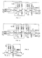
- Fig 1: Kompensation des Emitterbahnwiderstands für eine Multipliziererschaltung nach "2" für niedrige Steuerströme, nichtinvertierende Beschaltung.
- Fig 2: Gleich wie Fig 1, jedoch für größere Steuerströme bzw für fix eingestellten Steuerstrom des ersten Differenzverstärkers.
- Fig 3: Kompensation des Emitterbahnwiderstandes für einfache Multipliziererschaltungen nach Abb 12.37 aus "1".
- Fig. 1: Compensation of the emitter path resistance for a multiplier circuit according to "2" for low control currents, non-inverting wiring.
- Fig. 2: Same as Fig. 1, but for larger control currents or for a fixed control current of the first differential amplifier.
- Fig. 3: Compensation of the emitter path resistance for simple multiplier circuits according to Fig. 12.37 from "1".
Eine der möglichen Ausführungen für die Beseitigung der durch die Emitterbahnwiderstände verursachten Nichtlinearität bei Multipliziererschaltungen, bei denen Eingangssignal auf einen Eingangsverstärker gegeben wird, in dessen Gegenkopplung ein erster Differenzverstärker angeordnet ist und ein Eingang des ersten ersten Differenzverstärkers mit einem Eingang des zweiten Differenzverstärkers verbunden ist, weiters die Kollektoren des zweiten Differenzverstärkers mit den Eingängen eines Ausgangsverstärkers verbunden sind und die Multiplikation des Eingangssignals mit einem Faktor durch Steuerung des Stromes in den Emmiterzweigen erfolgt, wird nun anhand der Fig 1 näher erläutert. Es wird dort also mittels zweier Spannungsteiler, Rb1, Rb2 und Rd1, Rd2, ein proportionaler Anteil des Eingangssignals (uE) auf den zweiten Eingang (B) des ersten Differenzverstärkers (D1) und ein proportionaler Anteil des Ausgangssignals (uA) auf den zweiten Eingang (D) des zweiten Differenzverstärkers (D2) gegeben. Beim zweiten Differenzverstärker erfolgt die Mitkopplung abhängig von der Größe des Ausgangssignals und damit vom Steuerstrom ID2 über A2, den zweiten Spannungsteiler Rd1, Rd2 und den Eingang D des Transistors T4. Etwas anders sind die Verhältnisse beim ersten Differenzverstärker (D1): Dort steigt mit größer werdendem Steuerstrom ID1 die Gegenkopplung über den Eingangsverstärker (A1) an, sodaß die Ausgangsspannung von A1 bei gleichbleibendem Eingangssignal (uE) sinkt, das am Eingang B des Transistors T2 anliegende Signal jedoch gleich bleibt und somit steigt auch beim D1 das Signal am zweiten Eingang (B) relativ zum am Eingang A anliegenden Signal an, wenn ID1 vergrößert wird. Es ist also für beide Differenzverstärker gewährleistet, daß die Größe der Kompensationsspannungen vom jeweiligen Steuerstrom ID1 bzw ID2 abhängt. Da man auch annehmen kann, daß die Emitterbahnwiderstände weitgehend unabhängig von den Steuerströmen sind, kann bei richtiger Einstellung der beiden Spannungsteiler Rb1, Rb2 und Rd1, Rd2, die durch den R-Eb verursachte schädliche Gegenkopplung praktisch kompensiert werden.One of the possible designs for eliminating the non-linearity caused by the emitter path resistances in multiplier circuits in which an input signal is applied to an input amplifier, in the negative feedback of which a first differential amplifier is arranged and an input of the first first differential amplifier is connected to an input of the second differential amplifier the collectors of the second differential amplifier are connected to the inputs of an output amplifier and the multiplication of the input signal by a factor by controlling the current in the emitter branches is now explained in more detail with reference to FIG. 1. It is there by means of two voltage dividers, Rb1, Rb2 and Rd1, Rd2, a proportional part of the input signal (uE) to the second input (B) of the first differential amplifier (D1) and a proportional part of the output signal (uA) to the second input (D) of the second differential amplifier (D2). In the second differential amplifier, the positive feedback takes place depending on the size of the output signal and thus on the control current ID2 via A2, the second voltage divider Rd1, Rd2 and the input D of the transistor T4. The situation is somewhat different for the first differential amplifier (D1): there, with increasing control current ID1, the negative feedback via the input amplifier (A1) increases, so that the output voltage of A1 drops with the input signal (uE) remaining constant at the input B of transistor T2 However, the signal remains the same and thus also with D1 the signal at the second input (B) increases relative to the signal at input A if ID1 is increased. It is thus guaranteed for both differential amplifiers that the magnitude of the compensation voltages from the respective control current ID1 or ID2 depends. Since it can also be assumed that the emitter path resistances are largely independent of the control currents, if the two voltage dividers Rb1, Rb2 and Rd1, Rd2 are set correctly, the harmful negative feedback caused by the R-Eb can be practically compensated for.
Folgende Ursache ist dafür verantwortlich, daß die Kompensation des R-Eb nach Fig 1 nicht 100%ig ist: Die störende Gegenkopplung wirkt nicht nur für die an den jeweils ersten Eingängen (A, C) der beiden Differenzverstärker anliegenden Signale, sondern auch gleichermaßen für die an den jeweils zweiten Eingängen (B, D) anliegenden Kompensationssignale und daher bleibt ein Rest-Verstärkungsfehler ΔV-R übrig. Die Auswirkung des ΔV-R hängt von den jeweiligen Steuerströmen ab, bei denen die beiden Spannungsteiler (Rb1, Rb2 und Rd1, Rd2) auf die niedrigste Nichtlinearität eingestellt werden und steigt bei größeren maximalen Werten für die beiden Steuerströme. Aus dem genannten Grund ist dann die in Fig 2 gezeigte Kompensation des R-Eb im Vorteil gegenüber der in Fig 1 gezeigten, wenn ID1 einen nicht veränderbaren, festen Wert hat. Dann ist nämlich der ΔV-R für den ersten Differenzverstärker konstant und wenn wie in Fig 2 der Ausgangsverstärker gegenüber Fig 1 invertierend beschalten ist, kann der proportionale Anteil von uA am Eingang B mit dem proportionalen Anteil von uE summiert werden. Somit wirkt bei konstantem ID1 für beide Kompensationsspannungen ein gleich großer und konstanter ΔV-R und dieser kann bei der Einstellung von Rb1 und Rb3 mitberücksichtigt werden, womit die Kompensation des R-Eb nun zu 100% erfolgen kann.The following cause is responsible for the fact that the compensation of the R-Eb according to FIG. 1 is not 100%: The disturbing negative feedback acts not only for the signals present at the first inputs (A, C) of the two differential amplifiers, but also equally the compensation signals present at the respective second inputs (B, D) and therefore a residual gain error ΔV-R remains. The effect of the ΔV-R depends on the respective control currents at which the two voltage dividers (Rb1, Rb2 and Rd1, Rd2) are set to the lowest non-linearity and increases with larger maximum values for the two control currents. For the above-mentioned reason, the compensation of the R-Eb shown in FIG. 2 has an advantage over that shown in FIG. 1 if ID1 has a fixed value that cannot be changed. Then the ΔV-R for the first differential amplifier is constant and if, as in FIG. 2, the output amplifier is wired inverting with respect to FIG. 1, the proportional component of uA at input B can be summed with the proportional component of uE. Thus, with constant ID1, an equal and constant ΔV-R acts for both compensation voltages and this can be taken into account when setting Rb1 and Rb3, so that the compensation of R-Eb can now be carried out 100%.
Als willkommener zusätzlicher Effekt vermindern bzw beseitigen die in Fig. 1 und Fig 2 abgebildeten Emitterbahnwiderstands-Kompensationen auch noch die Nichtlinearität der Steuerstrom-Gesamtverstärkungskennlinie, die ihre Ursache ebenfalls in der, bei steigenden Steuerströmen steigen den Gegenkopplung in den beiden Differenzverstärkern hat.As a welcome additional effect, the emitter path resistance compensations shown in FIGS. 1 and 2 also reduce or eliminate the non-linearity of the overall control current gain characteristic, which is also due to the fact that with increasing control currents the negative feedback increases in the two differential amplifiers.
Es gibt Anwendungen, bei denen nicht eine Reduktion, sondern eine gezielte Anhebung der kubischen Verzerrungen erwünscht ist. Bei Musikerverstärkern wird dies zur Erzielung eines besseren Klanges sehr oft angewandt. Wenn nun ein proportionaler Anteil von uE auf den Eingang D gegeben wird, so kann bei dementsprechendem Anteil von uE der kubische Verzerrungsgrad so eingestellt werden, daß das "weiche" Übersteuerungsverhalten von Röhrenverstärkern nachgebildet werden kann. Zusätzlich zur Anwendung der Schaltung zur Beeinflussung des Dynamikverhaltens der verschiedensten Signalquellen kann mit demselben Baustein auch das kubische Klirrverhalten beliebig beeinflußt werden.There are applications in which a reduction in the cubic distortion is desired, rather a targeted increase. This is very often used for music amplifiers to achieve better sound. If a proportional portion of uE is now applied to input D, the cubic degree of distortion can be adjusted so that the "soft" clipping behavior of tube amplifiers can be simulated with the corresponding portion of uE. In addition to using the circuit to influence the dynamic behavior of the A wide variety of signal sources can be used to influence the cubic distortion behavior as desired.
Schließlich ist aus Fig 3 ersichtlich, wie auch die Eigenschaften von einfachen Multipliziererschaltungen nach Abb 12.37 aus "1" durch die Kompensation des R-Eb verbessert werden können: Gleich wie beim zweiten Differenzverstärker (D2) in Fig 1 wird in Fig 3 die schädliche Gegenkopplung durch eine Mitkopplung über den Spannungsteiler Rd1, Rd2 kompensiert und damit die Steuerstrom-Gesamtverstärkungsskennlinie linearisiert.Finally, it can be seen from FIG. 3 how the properties of simple multiplier circuits according to FIG. 12.37 from “1” can be improved by compensating the R-Eb: As in the second differential amplifier (D2) in FIG. 1, the harmful negative feedback is shown in FIG compensated by a positive feedback via the voltage divider Rd1, Rd2 and thus linearized the overall control current gain characteristic.
Bauteilewerte (Beispiel) zu Fig 1:
RE1 = RE2 = RA1 = RA2 = 1 kOhm
Rb2 = Rd2 = 10 Ohm
Rb1 = Rd1 = ca 40 kOhm (R-Eb von T1-4 = ca 0.5 Ohm)Component values (example) for Fig 1:
RE1 = RE2 = RA1 = RA2 = 1 kOhm
Rb2 = Rd2 = 10 ohms
Rb1 = Rd1 = approx. 40 kOhm (R-Eb from T1-4 = approx. 0.5 Ohm)
Claims (2)
Applications Claiming Priority (2)
| Application Number | Priority Date | Filing Date | Title |
|---|---|---|---|
| AT342287A AT392709B (en) | 1987-12-23 | 1987-12-23 | ELECTRONIC MULTIPLIER CIRCUIT |
| AT3422/87 | 1987-12-23 |
Publications (2)
| Publication Number | Publication Date |
|---|---|
| EP0324967A2 true EP0324967A2 (en) | 1989-07-26 |
| EP0324967A3 EP0324967A3 (en) | 1990-09-26 |
Family
ID=3550283
Family Applications (1)
| Application Number | Title | Priority Date | Filing Date |
|---|---|---|---|
| EP19880121488 Withdrawn EP0324967A3 (en) | 1987-12-23 | 1988-12-22 | Linearly compensated slope multiplier |
Country Status (2)
| Country | Link |
|---|---|
| EP (1) | EP0324967A3 (en) |
| AT (1) | AT392709B (en) |
Cited By (1)
| Publication number | Priority date | Publication date | Assignee | Title |
|---|---|---|---|---|
| US6043768A (en) * | 1996-02-16 | 2000-03-28 | Johannes Heidenhain Gmbh | Device and method for switching between different operating modes of a transducer |
Citations (2)
| Publication number | Priority date | Publication date | Assignee | Title |
|---|---|---|---|---|
| US3562553A (en) * | 1968-10-21 | 1971-02-09 | Allen R Roth | Multiplier circuit |
| EP0157520A2 (en) * | 1984-04-02 | 1985-10-09 | Precision Monolithics Inc. | Analog multiplier with improved linearity |
-
1987
- 1987-12-23 AT AT342287A patent/AT392709B/en not_active IP Right Cessation
-
1988
- 1988-12-22 EP EP19880121488 patent/EP0324967A3/en not_active Withdrawn
Patent Citations (2)
| Publication number | Priority date | Publication date | Assignee | Title |
|---|---|---|---|---|
| US3562553A (en) * | 1968-10-21 | 1971-02-09 | Allen R Roth | Multiplier circuit |
| EP0157520A2 (en) * | 1984-04-02 | 1985-10-09 | Precision Monolithics Inc. | Analog multiplier with improved linearity |
Non-Patent Citations (2)
| Title |
|---|
| ELECTRONICS & WIRELESS WORLD, Band 91, Nr. 1596, Oktober 1985, Seiten 27-31, Sutton, Surrey, GB; J. LIDGEY: "The tale of the long-tail pair - part 2" * |
| J.G. GRAEME et al.: "Operational Amplifiers, Design and Applications", 1971, Seiten 275-279, McGraw-Hill, New York, US * |
Cited By (1)
| Publication number | Priority date | Publication date | Assignee | Title |
|---|---|---|---|---|
| US6043768A (en) * | 1996-02-16 | 2000-03-28 | Johannes Heidenhain Gmbh | Device and method for switching between different operating modes of a transducer |
Also Published As
| Publication number | Publication date |
|---|---|
| EP0324967A3 (en) | 1990-09-26 |
| AT392709B (en) | 1991-05-27 |
| ATA342287A (en) | 1990-10-15 |
Similar Documents
| Publication | Publication Date | Title |
|---|---|---|
| KR910001630B1 (en) | Tunable active filter | |
| DE60132860T2 (en) | transconductance amplifier | |
| DE2429953B2 (en) | Circuit arrangement for processing physiological measurement signals | |
| DE102007011715B4 (en) | Amplifier arrangement for amplifying a signal | |
| EP0365085B1 (en) | Signal amplitude controlling circuit | |
| DE3108617A1 (en) | "GAIN CONTROL CIRCUIT" | |
| DE3024142A1 (en) | CIRCUIT ARRANGEMENT WITH TWO CROSS-DIFFERENTIAL AMPLIFIERS | |
| DE19518734C1 (en) | Transimpedance amplifier circuit with controlled impedance | |
| US6023194A (en) | Amplifier with reduced input capacitance | |
| US4234804A (en) | Signal correction for electrical gain control systems | |
| DE2852567A1 (en) | AMPLIFIERS WITH A FIRST AND A SECOND AMPLIFIER ELEMENT | |
| EP0324967A2 (en) | Linearly compensated slope multiplier | |
| DE4104980C2 (en) | Amplifier stage for low-impedance AC sources | |
| DE69838349T2 (en) | Signal converter for tube amplifiers | |
| DE2755827A1 (en) | CIRCUIT ARRANGEMENT WITH A FREQUENCY RESPONSE THAT CAN BE CHANGED BY A CONTROL VOLTAGE | |
| DE102019132693A1 (en) | Amplifier circuit with a current-voltage converter for reading out a photodiode of an electron microscope | |
| DE3439116A1 (en) | AMPLIFIER CIRCUIT | |
| DE3124328C2 (en) | Variable active equalizer | |
| DE2646386A1 (en) | Isolation amplifier for video signal switching network - has complementary push-pull output transistors driven by complementary input transistors | |
| DE19637292B4 (en) | Amplifier circuit, in particular for amplifying audio signals and audio amplifiers | |
| EP1599936B1 (en) | Transimpedance amplifier with a high gain bandwidth for converting a dac-output current | |
| DE3814604A1 (en) | SOUND FREQUENCY AMPLIFIER IN BRIDGE ARRANGEMENT | |
| DE69826806T2 (en) | LINE DRIVER WITH ADAPTIVE OUTPUT SIMPEDANCE | |
| DE1772169C (en) | Amplifier with interference frequency suppression | |
| EP0324525A2 (en) | Amplifier circuit |
Legal Events
| Date | Code | Title | Description |
|---|---|---|---|
| PUAI | Public reference made under article 153(3) epc to a published international application that has entered the european phase |
Free format text: ORIGINAL CODE: 0009012 |
|
| AK | Designated contracting states |
Kind code of ref document: A2 Designated state(s): BE CH DE ES FR GB GR IT LI LU NL SE |
|
| RBV | Designated contracting states (corrected) |
Designated state(s): CH DE ES FR GB IT LI LU NL SE |
|
| 17P | Request for examination filed |
Effective date: 19900310 |
|
| PUAL | Search report despatched |
Free format text: ORIGINAL CODE: 0009013 |
|
| AK | Designated contracting states |
Kind code of ref document: A3 Designated state(s): BE CH DE ES FR GB GR IT LI LU NL SE |
|
| STAA | Information on the status of an ep patent application or granted ep patent |
Free format text: STATUS: THE APPLICATION IS DEEMED TO BE WITHDRAWN |
|
| 18D | Application deemed to be withdrawn |
Effective date: 19930701 |