EP0330148B1 - Circuit breaker - Google Patents
Circuit breaker Download PDFInfo
- Publication number
- EP0330148B1 EP0330148B1 EP89103002A EP89103002A EP0330148B1 EP 0330148 B1 EP0330148 B1 EP 0330148B1 EP 89103002 A EP89103002 A EP 89103002A EP 89103002 A EP89103002 A EP 89103002A EP 0330148 B1 EP0330148 B1 EP 0330148B1
- Authority
- EP
- European Patent Office
- Prior art keywords
- circuit
- voltage
- current
- output
- electric power
- Prior art date
- Legal status (The legal status is an assumption and is not a legal conclusion. Google has not performed a legal analysis and makes no representation as to the accuracy of the status listed.)
- Expired - Lifetime
Links
Images


Classifications
-
- H—ELECTRICITY
- H01—ELECTRIC ELEMENTS
- H01H—ELECTRIC SWITCHES; RELAYS; SELECTORS; EMERGENCY PROTECTIVE DEVICES
- H01H9/00—Details of switching devices, not covered by groups H01H1/00 - H01H7/00
- H01H9/54—Circuit arrangements not adapted to a particular application of the switching device and for which no provision exists elsewhere
-
- H—ELECTRICITY
- H02—GENERATION; CONVERSION OR DISTRIBUTION OF ELECTRIC POWER
- H02H—EMERGENCY PROTECTIVE CIRCUIT ARRANGEMENTS
- H02H3/00—Emergency protective circuit arrangements for automatic disconnection directly responsive to an undesired change from normal electric working condition with or without subsequent reconnection ; integrated protection
- H02H3/08—Emergency protective circuit arrangements for automatic disconnection directly responsive to an undesired change from normal electric working condition with or without subsequent reconnection ; integrated protection responsive to excess current
- H02H3/093—Emergency protective circuit arrangements for automatic disconnection directly responsive to an undesired change from normal electric working condition with or without subsequent reconnection ; integrated protection responsive to excess current with timing means
-
- H—ELECTRICITY
- H01—ELECTRIC ELEMENTS
- H01H—ELECTRIC SWITCHES; RELAYS; SELECTORS; EMERGENCY PROTECTIVE DEVICES
- H01H71/00—Details of the protective switches or relays covered by groups H01H73/00 - H01H83/00
-
- H—ELECTRICITY
- H02—GENERATION; CONVERSION OR DISTRIBUTION OF ELECTRIC POWER
- H02H—EMERGENCY PROTECTIVE CIRCUIT ARRANGEMENTS
- H02H3/00—Emergency protective circuit arrangements for automatic disconnection directly responsive to an undesired change from normal electric working condition with or without subsequent reconnection ; integrated protection
- H02H3/02—Details
- H02H3/04—Details with warning or supervision in addition to disconnection, e.g. for indicating that protective apparatus has functioned
- H02H3/044—Checking correct functioning of protective arrangements, e.g. by simulating a fault
Definitions
- the present invention relates to a circuit breaker having an overcurrent tripping characteristic, and especially relates to the testing of the tripping characteristic of the circuit breaker.
- value of the current flowing the shunt circuit does not correspond to the current flowing on the A.C. power lines.
- errors are contained among level detection of the accident overcurrent.
- the value of the current flowing in the shunt circuit is not kept constant, and therefore it is difficult to compensate the error of the level detection of the accident overcurrent.
- the conventional circuit breaker does not have means for checking the tripping characteristic. Therefore, it is very difficult and dangerous to check the tripping characteristic of the circuit breaker when actually used.
- Document US-A-4 060 844 relates to a circuit breaker apparatus comprising at least one current transformer, at least one rectifying circuit, a series connection of an electric power circuit and at least one resistor connected between the output terminals of the rectifying circuit. Furthermore, a pair of test points is provided in order to enable an externally controlled test of the apparatus. It is suggested to couple a current source between the test points, to vary the test current and to compare the time interval between application of the test current and actuation of a contact separation mechanism to the desired current-versus-time response curve. However, a complete test circuit within the apparatus is not provided.
- the circuit breaker in accordance with the present invention comprises: at least one current transformer for detecting the current flowing in at least one AC power line; at least one rectifying circuit for converting the AC output current from the secondary winding of said current transformer to an unidirectional current; a series connection of an electric power circuit and at least one resistor connected between the output terminals of the rectifying circuit, said resistor converting the current flowing thereon to a voltage representative of the current in the AC power line; test means for applying a test signal to the circuit breaker, said test means comprising at least one connector having plural contacts for supplying a DC voltage from an external power source to said electric power circuit and a reverse current preventing device connected between the electric power circuit and a contact of the connector; the circuit breaker comprises at least one differential amplifier for amplifying said voltage across both ends of said resistor; and the test means further comprises at least one DC power source for outputting a test voltage, at least one switch connected between said test voltage DC power source and an input of said differential amplifier, and at least one test signal generating circuit for generating an
- the circuit breaker in accordance with the present invention is constituted as mentioned above. Therefore, the A.C. output of the secondary winding of the current transformer, which is in proportion to the current value flowing on the A.C. power line, is converted to a unidirectional current by the rectifying circuit. The whole unidirectional current is led to the electric power circuit and the resistor for detecting the current value. Namely, the whole secondary output current of the current transformer flows on the resistor, so that no error is produced in detected result on the overcurrent. As a result, accuracy of level detection of an accident overcurrent is improved.
- the circuit breaker has a test signal generating circuit, thereby application of the test voltage from the D.C. power source to the differential amplifier is made by switching on and off. As a result, checking of tripping characteristics of the circuit breaker is easily made on the circuit breaker which is actually connected in the power line and in use now.
- the circuit breaker in accordance with the present invention has a reverse current preventing device connected between the electric power circuit and the contacts. Therefore, even when all the contacts are short-circuited under condition that the A.C. power line is active, the secondary current from the current transformer may not be supplied to the contacts. As a result, desired overcurrent tripping is achieved.
- FIG.1 is a circuit diagram showing a preferred embodiment of a circuit breaker in accordance with the present invention.
- FIG.2 is a circuit diagram showing details of an electric power circuit and an insufficient voltage locking circuit in the circuit breaker in accordance with the present invention.
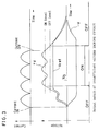
- FIG.3 is a time chart showing operations of the electric power circuit and the insufficient voltage locking circuit of the circuit breaker in accordance with the present invention.
- FIG.4 is a drawing showing the relation between output voltage of a differential amplifier 63 shown in FIG.1 and the voltage applied thereto.
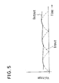
- FIG.5 is a drawing showing an input voltage and an output voltage of peak value converting circuits 210, 210 as shown in FIG.1.
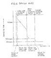
- FIG.6 is a drawing showing tripping characteristics of a known circuit breaker.
- FIG.1, FIG.2, FIG.3, FIG.4, FIG.5 and FIG.6 A preferred embodiment of a circuit breaker in accordance with the present invention is described referring to FIG.1, FIG.2, FIG.3, FIG.4, FIG.5 and FIG.6.
- FIG.1 is a circuit diagram showing a circuit breaker in accordance with the present invention.
- a circuit breaker of a single phase are shown for making the description simple, but the actual system has three power lines and three circuit breakers of the same constitution.
- a terminal on electric power side 101 is to be connected to an A.C. electric power source (not shown) and a load break contact 201 is connected to the terminal on the electric power side 101.
- the A.C. power line 1 is connected between the load break contact 201 and a terminal on load side 301.
- a current transformer 21 is provided on the A.C. power line 1 between the terminal on electric power side 101 and the terminal on the load side 301.
- a rectifying circuit 30 is connected to secondary output terminals of the current transformer 21 for changing an alternating current flowing on secondary winding of the current transformer 21 to a unidirectional current.
- the rectifying circuit 30 consists of two sets of series circuits of diodes.
- An electric power circuit 500 for outputting a D.C. constant voltage is connected to a positive output terminal of the rectifying circuit 30.
- the electric power circuit 500 has a positive terminal 5a, a reference output terminal 5b, a middle output terminal 5c and a negative output terminal 5d.
- FIG.2 shows a preferred embodiment of the electric power circuit 500 shown in FIG.1.
- an impedance circuit 501 which makes tripping operation of an electromagnetic tripping apparatus easy, comprises: a series connection of resistors R4 and R5 connected between an output terminal 30a of the rectifying circuit 30 and the collector of a transistor Tr1; a resistor R6 connected between the connection point 501a of the resistors R4 and R5 and the base of the transistor Tr1; and a zener diode ZD1 connected between the connection point 501a of the resistors R4 and R5 and the emitter of the transistor Tr1.
- a voltage restriction device 502 such as a zener diode is connected to the impedance circuit 501 as series connection.
- the anode of a diode 503 is connected to the connection point 501b of the impedance circuit and the voltage restriction device 502.
- a smoothing capacitor 504 is connected between the cathode of the diode 503 and the negative terminal 5d of the electric power circuit 500.
- the cathode of the diode 503 is further connected to the positive terminal 5a of the electric power circuit 500.
- a reference voltage generating circuit 505 is connected to the positive terminal 5a of the electric power circuit 500.
- Another voltage restriction device 506 such as a zener diode is connected in series to the reference voltage generating circuit 505.
- the connection point 505a of the reference voltage generating circuit 505 and the voltage restriction device 506 is connected to the middle terminal 5c of the electric power circuit 500.
- an output terminal 505b of the reference voltage generating circuit 500 is connected to a reference terminal 5b of the electric power circuit 500.
- the negative terminal 5d of the electric power circuit 500 is connected to a terminal of a resistor 40 for current detection.
- the other terminal of the resistor 40 is connected to a terminal of another resistor 41 for current detection.
- the other teminal of the resistor 41 is connected to the negative terminal of the rectifying circuit 30.
- Differential amplifiers 60, 61 respectively consist of an operational amplifier 63 or 631 and four resistors 64, 65, 66 and 67 or 641, 651, 661 and 671. Electric power is supplied to the differential amplifiers 60 and 61 from the electric power circuit 500. Input terminals of the differential amplifiers 60 and 61 are respectively connected to both terminals of the resistors 40 and 41. The differential amplifiers 60 and 61, convert voltage drop of the resistors 40 and 41 for current detection respectively to a voltage signal based on a middle voltage Vo of the electric power source 500.
- the relation of gains of the differential amplifiers 60 and 61 are selected such that the gain of the one nearer to the electric power circuit 500 is smaller than that of the other. In this embodiment, the relation is concluded that the gain of the differential amplifier 60 is smaller than that of the differential amplifier 61.
- a time delay circuit 70 comprises an instant time tripping circuit 230, a short time tripping circuit 220 and a long time tripping circuit 170. Respective output terminals of the instant time tripping circuit 230, the short time tripping circuit 220 and the long time tripping circuit 170 are connected commonly to an output terminal 70a of the time delay circuit 70.
- the instant time tripping circuit 230 is connected to the output terminal of the differential amplifier 60.
- a a series connection of a peak value conversion circuit 210 and the short time tripping circuit 220 and another series connection of an effective value conversion circuit 211 and the long time tripping circuit 170 are connected to the instant time tripping circuit 230 as parallel connection.
- the instant time tripping circuit 230 outputs a trip signal at the time when the input signal thereto becoms above a first predetermined value.
- the short time tripping circuit 220 outputs a trip signal shortly after the input of peak value from the peak value conversion circuit 210 becomes above a second predetermined value.
- the long time tripping circuit 170 outputs a trip signal after a predetermined long time period from when the input of effective value from the effective value conversion circuit 211 becomes above a third predetermined value.
- An electromagnetic tripping coil 80 is connected to a positive teminal of the rectifying circuit 30.
- a switching circuit 120 is connected between the electromagnetic tripping coil 80 and the negative terminal 5d of the electric power circuit 500.
- the electromagnetic tripping coil 80 is mechanically linked to the tripping mechanism 100 for opening the load break contact 201 provided on the A.C. power line 1 and is excited for driving the tripping mechanism 100 when the switching circuit 120 turns on.
- An insufficient voltage operation locking circuit 50 for locking the tripping operation when the voltage of the electric power circuit 500 is insufficient (is below a predetermined voltage), has an output switch 54 which is connected between the switching circuit 120 and the time delay circuit 70.
- the insufficient voltage operation locking circuit 50 comprises a comparator 53 and a potential divider 51 as shown in FIG.2.
- the potential divider 51 consists of the series connection of resistors R7 and R8 connected between the positive terminal 5a and the middle terminal 5c of the electric power circuit 500.
- the connection point 51a of the resistors R7 and R8 is connected to one input terminal of the comparator 53 and the other input terminal of the comparator 53 is connected to the reference terminal 5b of the electric power circuit 500.
- a connector 11 for testing operation has contacts 11a, 11b, 11c and 11d.
- the contact 11a is connected to the negative terminal 5d of the electric power circuit 500.
- the contact 11b is connected to the anode of a diode 12 which is used for preventing revers current to the contacts and the cathode of the diode 12 is connected to the positive terminal 30a of the rectifying circuit 30.
- the contact 11c is connected to a first test signal generating circuit 13 and the contact 11d is connected to a second test signal generating circuit 14.
- Terminals 15a, 15b, 15c and 15d are disconnectably connected to the contacts 11a, 11b, 11c, and 11d respectively.
- the terminal 15a is connected to the negative electrode of a D.C. power source 16.
- Other terminals 15b, 15c and 15d are respectively connected to switches 17a, 17b and 17c.
- the switches 17a, 17b and 17c are connected to the positive electrode of the D.C. power source 16.
- a secondary alternating electric current having a value defined by the ratio of current transformation flows on a secondary winding of the current transformer 21.
- the secondary alternating electric current is converted to a unidirectional electric current by the rectifying circuit 30.
- the output current of the rectifying circuit 30 flows through the electric power circuit 500 and the resistors 40 and 41. And the output current circulates to the rectifying circuit 30.
- a current having waveforms of full wave rectification corresponding to the current flowing on the A.C. power line 1 flows on the electric power circuit 500 and the resistors 40 and 41.
- the output voltage of the electric power circuit 500 is also applied to the insufficient voltage operation locking circuit 50.
- the comparator 53 which shows hysteresis turns the switch 54 on. And when the voltage +V becomes smaller than OFF level, the comparator 53 turns the switch 54 off.
- the difference between the ON level and the OFF level is selected to be larger than the above-mentioned ripple component contained in the voltage +V, and thereby the switch 54 may not repeat the switching on and off by the ripple component.
- the insufficient voltage operation locking circuit 50 turns the switch 54 on only when all of the following conditions are satisfied simultaneously: the voltage +V is over a predetermined value; the voltage Vref is fully stable; and the voltage -V reaches a predetermined value.
- the instant time tripping circuit 230 issues an output signal as an output of the time delay circuit 70.
- the output of the differential amplifier 60 is applied to the peak value conversion circuits 210 and 210. Waveforms of the peak value conversion circuit 210 and 210 are, for example, shown in FIG.5. Outputs of the peak value conversion circuits 210 and 210 are respectively applied to the short time tripping circuit 220, and the long time tripping circuit 170.
- the short time tripping circuit 220 and the long time tripping circuit 170 respectively issue output signal as an output of the time delay circuit 70.
- the output signal of the time delay circuit 70 passes the output switch 54 of the insufficient voltage operation locking circuit 50 and triggers the switching circuit 120 to produce an input. Thereby, the switching circuit 120 is turned on and the electromagnetic tripping coil 80 is excited. When the electromagnetic tripping coil 80 is excited, the load break contact 201 which is linked to the electromagnetic tripping coil 80 by the tripping mechanism 100 shown in FIG.1 is opened for breaking the accidental overcurrent. Such a tripping operation is, for example, shown is FIG.6.
- the electric power circuit 500 may output insufficient voltage for driving the time delay circuit 70.
- the output switch 54 of the insufficient voltage operation locking circuit 50 turns off to prevent the switching on of the switching circuit 120, even when the time delay circuit 70 outputs an erroneous output.
- terminals 15a, 15b, 15c and 15d are respectively connected to the contacts 11a, 11b, 11c and 11d of the connector 11.
- the switch 18 is turned to be connected to the first D.C. power source 19 by the output of the first test signal generating circuit 13.
- the voltage from the first D.C. power source 19 is applied to the positive input terminal of the differential amplifier 60 as an input signal and the output signal of the differential amplifier 60 is applied to the time delay circuit 70.
- the instant time tripping circuit 230 issues an output in the instant time tripping region shown in FIGs.4 and 6 as an output of the time delay circuit 70.
- the switch 22 is turned to be connected to the second D.C. power source 20 by the output of the second test signal generating circuit 14.
- the voltage from the second D.C. power source 20 is applied to the positive input terminal of the differential amplifier 61 as an input signal.
- the output signal of the differential amplifier 61 is applied to the time delay circuit 70.
- the long time tripping circuit 170 issues an output in the long time tripping region shown in FIGs. 4 and 6 as an output of the time delay circuit 70.
- checking of the instant time tripping characteristic and the long time tripping characteristic in the state that the circuit breaker is actually connected in the power line for use can easily be executed by following steps of: connecting the terminals 15a, 15b, 15c and 15d to the contacts 11a, 11b, 11c and 11d of the connector 11 respectively for testing operation and turning on the switch 17a; supplying the voltage of the D.C. power source 16 to the electric power circuit 500; closing the switch 17b or 17c; turning the switch 18 or 22 to be connected to the D.C. power source 19 or 20 by the output of the first or second test signal generating circuit 13 or 14; and applying the output voltage of the first or second D.C. power source 19 or 20 as a quasi input signal or test signal to the differential amplifier 60 or 61.
- a circuit breaker for breaking two or three phase A.C. power lines can be realized by comprising: plural current transformers for converting currents flowing on the two or three phases to output currents of secondary winding in proportion to predetermined ratio of current transformation; plural rectifying circuits for converting the alternating secondary output current of the current transformers to unidirectional currents; series connection of plural (four to six) resistors which are also connected to an electric power circuit whereon the output current of the rectifying circuits flow; and plural sets of differential amplifier, test signal generating circuit, switch and so on corresponding to respective resistors.
- the circuit breaker for plural phases of A.C. power lines has checking function of the tripping characteristics similar to the afore-mentioned embodiment.
Description
- The present invention relates to a circuit breaker having an overcurrent tripping characteristic, and especially relates to the testing of the tripping characteristic of the circuit breaker.
- In a conventional circuit breaker, for example, shown in Published Unexamined Japanese Patent Application Sho 60-32211, output currents of secondary windings of current transformers, as current detection means, flow in rectifying circuits. A part of D.C. voltage from the rectifying circuit is applied to an electric power circuit of a signal processing circuit such as a microcomputer and the remainder of the D.C. voltage than the rectifying circuit is applied to a shunt circuit, whose output is for being used as control signals of the signal processing circuit.
- When a part of the secondary output currents of the current transformers for detecting current values of A.C. power lines flow to the electric power circuit, value of the current flowing the shunt circuit does not correspond to the current flowing on the A.C. power lines. As a result, errors are contained among level detection of the accident overcurrent. Furthermore, the value of the current flowing in the shunt circuit is not kept constant, and therefore it is difficult to compensate the error of the level detection of the accident overcurrent.
- Still more, the conventional circuit breaker does not have means for checking the tripping characteristic. Therefore, it is very difficult and dangerous to check the tripping characteristic of the circuit breaker when actually used.
- Document US-A-4 060 844 relates to a circuit breaker apparatus comprising at least one current transformer, at least one rectifying circuit, a series connection of an electric power circuit and at least one resistor connected between the output terminals of the rectifying circuit. Furthermore, a pair of test points is provided in order to enable an externally controlled test of the apparatus. It is suggested to couple a current source between the test points, to vary the test current and to compare the time interval between application of the test current and actuation of a contact separation mechanism to the desired current-versus-time response curve. However, a complete test circuit within the apparatus is not provided.
- It is an object of the present invention to provide an improved circuit breaker wherein accuracy of the level detection of the accident overcurrent is improved and the tripping characteristic is safely and easily checkable for the circuit breaker actually under use.
- The technical problem is solved by an apparatus in accordance with the new claim.
- The circuit breaker in accordance with the present invention comprises:
at least one current transformer for detecting the current flowing in at least one AC power line;
at least one rectifying circuit for converting the AC output current from the secondary winding of said current transformer to an unidirectional current;
a series connection of an electric power circuit and at least one resistor connected between the output terminals of the rectifying circuit, said resistor converting the current flowing thereon to a voltage representative of the current in the AC power line;
test means for applying a test signal to the circuit breaker, said test means comprising at least one connector having plural contacts for supplying a DC voltage from an external power source to said electric power circuit and a reverse current preventing device connected between the electric power circuit and a contact of the connector;
the circuit breaker comprises at least one differential amplifier for amplifying said voltage across both ends of said resistor; and
the test means further comprises at least one DC power source for outputting a test voltage, at least one switch connected between said test voltage DC power source and an input of said differential amplifier, and at least one test signal generating circuit for generating an output for controlling said switch on or off to apply said test voltage to the input of the differential amplifier when the switch is turned on, the test signal generating circuit receiving a DC voltage from said external power source through contacts of said connector. - The circuit breaker in accordance with the present invention is constituted as mentioned above. Therefore, the A.C. output of the secondary winding of the current transformer, which is in proportion to the current value flowing on the A.C. power line, is converted to a unidirectional current by the rectifying circuit. The whole unidirectional current is led to the electric power circuit and the resistor for detecting the current value. Namely, the whole secondary output current of the current transformer flows on the resistor, so that no error is produced in detected result on the overcurrent. As a result, accuracy of level detection of an accident overcurrent is improved.
- Furthermore, the circuit breaker has a test signal generating circuit, thereby application of the test voltage from the D.C. power source to the differential amplifier is made by switching on and off. As a result, checking of tripping characteristics of the circuit breaker is easily made on the circuit breaker which is actually connected in the power line and in use now.
- Still more, the circuit breaker in accordance with the present invention has a reverse current preventing device connected between the electric power circuit and the contacts. Therefore, even when all the contacts are short-circuited under condition that the A.C. power line is active, the secondary current from the current transformer may not be supplied to the contacts. As a result, desired overcurrent tripping is achieved.
- FIG.1 is a circuit diagram showing a preferred embodiment of a circuit breaker in accordance with the present invention.
- FIG.2 is a circuit diagram showing details of an electric power circuit and an insufficient voltage locking circuit in the circuit breaker in accordance with the present invention.
- FIG.3 is a time chart showing operations of the electric power circuit and the insufficient voltage locking circuit of the circuit breaker in accordance with the present invention.
- FIG.4 is a drawing showing the relation between output voltage of a differential amplifier 63 shown in FIG.1 and the voltage applied thereto.
- FIG.5 is a drawing showing an input voltage and an output voltage of peak
value converting circuits - FIG.6 is a drawing showing tripping characteristics of a known circuit breaker.
- A preferred embodiment of a circuit breaker in accordance with the present invention is described referring to FIG.1, FIG.2, FIG.3, FIG.4, FIG.5 and FIG.6.
- FIG.1 is a circuit diagram showing a circuit breaker in accordance with the present invention. In this embodiment, only a single phase of the power line and a circuit breaker of a single phase are shown for making the description simple, but the actual system has three power lines and three circuit breakers of the same constitution.
- In FIG.1, a terminal on
electric power side 101 is to be connected to an A.C. electric power source (not shown) and aload break contact 201 is connected to the terminal on theelectric power side 101. The A.C.power line 1 is connected between theload break contact 201 and a terminal onload side 301. Acurrent transformer 21 is provided on theA.C. power line 1 between the terminal onelectric power side 101 and the terminal on theload side 301. A rectifyingcircuit 30 is connected to secondary output terminals of thecurrent transformer 21 for changing an alternating current flowing on secondary winding of thecurrent transformer 21 to a unidirectional current. The rectifyingcircuit 30 consists of two sets of series circuits of diodes. Anelectric power circuit 500 for outputting a D.C. constant voltage is connected to a positive output terminal of the rectifyingcircuit 30. Theelectric power circuit 500 has apositive terminal 5a, areference output terminal 5b, amiddle output terminal 5c and anegative output terminal 5d. - FIG.2 shows a preferred embodiment of the
electric power circuit 500 shown in FIG.1. In FIG.2, animpedance circuit 501, which makes tripping operation of an electromagnetic tripping apparatus easy, comprises: a series connection of resistors R₄ and R₅ connected between anoutput terminal 30a of the rectifyingcircuit 30 and the collector of a transistor Tr₁; a resistor R₆ connected between theconnection point 501a of the resistors R₄ and R₅ and the base of the transistor Tr₁; and a zener diode ZD₁ connected between theconnection point 501a of the resistors R₄ and R₅ and the emitter of the transistor Tr₁. - A
voltage restriction device 502 such as a zener diode is connected to theimpedance circuit 501 as series connection. The anode of adiode 503 is connected to theconnection point 501b of the impedance circuit and thevoltage restriction device 502. Asmoothing capacitor 504 is connected between the cathode of thediode 503 and thenegative terminal 5d of theelectric power circuit 500. The cathode of thediode 503 is further connected to thepositive terminal 5a of theelectric power circuit 500. - A reference
voltage generating circuit 505 is connected to thepositive terminal 5a of theelectric power circuit 500. Anothervoltage restriction device 506 such as a zener diode is connected in series to the referencevoltage generating circuit 505. Theconnection point 505a of the referencevoltage generating circuit 505 and thevoltage restriction device 506 is connected to themiddle terminal 5c of theelectric power circuit 500. Furthermore, anoutput terminal 505b of the referencevoltage generating circuit 500 is connected to areference terminal 5b of theelectric power circuit 500. - In FIG.1, the
negative terminal 5d of theelectric power circuit 500 is connected to a terminal of aresistor 40 for current detection. The other terminal of theresistor 40 is connected to a terminal of another resistor 41 for current detection. The other teminal of the resistor 41 is connected to the negative terminal of the rectifyingcircuit 30. -
Differential amplifiers operational amplifier 63 or 631 and fourresistors differential amplifiers electric power circuit 500. Input terminals of thedifferential amplifiers resistors 40 and 41. Thedifferential amplifiers resistors 40 and 41 for current detection respectively to a voltage signal based on a middle voltage Vo of theelectric power source 500. The relation of gains of thedifferential amplifiers electric power circuit 500 is smaller than that of the other. In this embodiment, the relation is concluded that the gain of thedifferential amplifier 60 is smaller than that of thedifferential amplifier 61. - A
time delay circuit 70 comprises an instanttime tripping circuit 230, a shorttime tripping circuit 220 and a longtime tripping circuit 170. Respective output terminals of the instanttime tripping circuit 230, the shorttime tripping circuit 220 and the longtime tripping circuit 170 are connected commonly to anoutput terminal 70a of thetime delay circuit 70. - Namely, the instant
time tripping circuit 230 is connected to the output terminal of thedifferential amplifier 60. A a series connection of a peakvalue conversion circuit 210 and the shorttime tripping circuit 220 and another series connection of an effective value conversion circuit 211 and the longtime tripping circuit 170 are connected to the instanttime tripping circuit 230 as parallel connection. The instanttime tripping circuit 230 outputs a trip signal at the time when the input signal thereto becoms above a first predetermined value. The shorttime tripping circuit 220 outputs a trip signal shortly after the input of peak value from the peakvalue conversion circuit 210 becomes above a second predetermined value. The longtime tripping circuit 170 outputs a trip signal after a predetermined long time period from when the input of effective value from the effective value conversion circuit 211 becomes above a third predetermined value. - An electromagnetic tripping
coil 80 is connected to a positive teminal of the rectifyingcircuit 30. A switchingcircuit 120 is connected between the electromagnetic trippingcoil 80 and the negative terminal 5d of theelectric power circuit 500. The electromagnetic trippingcoil 80 is mechanically linked to the trippingmechanism 100 for opening theload break contact 201 provided on theA.C. power line 1 and is excited for driving the trippingmechanism 100 when theswitching circuit 120 turns on. - An insufficient voltage
operation locking circuit 50 for locking the tripping operation when the voltage of theelectric power circuit 500 is insufficient (is below a predetermined voltage), has anoutput switch 54 which is connected between the switchingcircuit 120 and thetime delay circuit 70. The insufficient voltageoperation locking circuit 50 comprises acomparator 53 and apotential divider 51 as shown in FIG.2. Thepotential divider 51 consists of the series connection of resistors R₇ and R₈ connected between thepositive terminal 5a and themiddle terminal 5c of theelectric power circuit 500. Theconnection point 51a of the resistors R₇ and R₈ is connected to one input terminal of thecomparator 53 and the other input terminal of thecomparator 53 is connected to thereference terminal 5b of theelectric power circuit 500. - In FIG.1, a connector 11 for testing operation has
contacts contact 11a is connected to the negative terminal 5d of theelectric power circuit 500. The contact 11b is connected to the anode of adiode 12 which is used for preventing revers current to the contacts and the cathode of thediode 12 is connected to thepositive terminal 30a of the rectifyingcircuit 30. The contact 11c is connected to a first testsignal generating circuit 13 and thecontact 11d is connected to a second testsignal generating circuit 14. - Terminals 15a, 15b, 15c and 15d are disconnectably connected to the
contacts D.C. power source 16. Other terminals 15b, 15c and 15d are respectively connected toswitches switches D.C. power source 16. - Operation of the above-mentioned circuit is described in the following.
- When a current flows on the
A.C. power line 1 of FIG.1, a secondary alternating electric current having a value defined by the ratio of current transformation flows on a secondary winding of thecurrent transformer 21. The secondary alternating electric current is converted to a unidirectional electric current by the rectifyingcircuit 30. The output current of the rectifyingcircuit 30 flows through theelectric power circuit 500 and theresistors 40 and 41. And the output current circulates to the rectifyingcircuit 30. At this time, a current having waveforms of full wave rectification corresponding to the current flowing on theA.C. power line 1 flows on theelectric power circuit 500 and theresistors 40 and 41. - When the current having waveforms of full wave rectification flows in the
electric power circuit 500, voltages +V, Vref, Vo and -V are generated on theterminals middle terminal 5c. In this case, the output voltage +V on theterminal 5a can contain ripple component. The relation between the output voltages +V and Vref is as follows:
- The output voltage of the
electric power circuit 500 is also applied to the insufficient voltageoperation locking circuit 50. When the voltage +V becomes larger than ON level shown in FIG.3, thecomparator 53 which shows hysteresis turns theswitch 54 on. And when the voltage +V becomes smaller than OFF level, thecomparator 53 turns theswitch 54 off. - The difference between the ON level and the OFF level is selected to be larger than the above-mentioned ripple component contained in the voltage +V, and thereby the
switch 54 may not repeat the switching on and off by the ripple component. - Namely, the insufficient voltage
operation locking circuit 50 turns theswitch 54 on only when all of the following conditions are satisfied simultaneously: the voltage +V is over a predetermined value; the voltage Vref is fully stable; and the voltage -V reaches a predetermined value. - On the other hand, electric power for the
differential amplifiers electric power circuit 500, and input voltages of thedifferential amplifiers resistors 40 and 41. Gains of thedifferential amplifiers differential amplifier 60 is smaller than that of thedifferential amplifier 61. Therefore, inclination of the output voltage characteristic of thedifferential amplifier 60 shown by A in FIG.4 can be made larger than that of the conventional one shown by C in the long time tripping region. As a result, a weak change of current value in the long time tripping region can be detected precisely. Hereupon, as the output voltage of the otherdifferential amplifier 61 has charge of the short time tripping region wherein change of current value is large, the incline of the output voltage characteristic shown by B is sufficient to be equal to the conventional one shown by C. - When an instant value of the output of the
differential amplifier 60 is above the instant time tripping region shown in FIG.4, the instanttime tripping circuit 230 issues an output signal as an output of thetime delay circuit 70. The output of thedifferential amplifier 60 is applied to the peakvalue conversion circuits value conversion circuit value conversion circuits time tripping circuit 220, and the longtime tripping circuit 170. When the values of the output current of the peakvalue conversion circuits time tripping circuit 220 and the longtime tripping circuit 170 respectively issue output signal as an output of thetime delay circuit 70. - The output signal of the
time delay circuit 70 passes theoutput switch 54 of the insufficient voltageoperation locking circuit 50 and triggers theswitching circuit 120 to produce an input. Thereby, theswitching circuit 120 is turned on and the electromagnetic trippingcoil 80 is excited. When the electromagnetic trippingcoil 80 is excited, theload break contact 201 which is linked to the electromagnetic trippingcoil 80 by the trippingmechanism 100 shown in FIG.1 is opened for breaking the accidental overcurrent. Such a tripping operation is, for example, shown is FIG.6. - When the value of the current flowing on the
load break contact 201 is smaller than 10--20% of the value of the rated current thereof, theelectric power circuit 500 may output insufficient voltage for driving thetime delay circuit 70. Under such a condition that the insufficient voltage state is outputted, theoutput switch 54 of the insufficient voltageoperation locking circuit 50 turns off to prevent the switching on of theswitching circuit 120, even when thetime delay circuit 70 outputs an erroneous output. - Next, testing operation of the above-mentioned circuit breaker in accordance with the present invention is described.
- At first, the terminals 15a, 15b, 15c and 15d are respectively connected to the
contacts - Under the condition that the
load break contact 201 is opened and any current does not flow on theA.C. power line 1, when the switch 17a is closed, a predetermined voltage, for example, 24V is applied to the electric power circuit from the outerD.C. power source 16, and direct current (D.C.) flows one theelectric power circuit 500. - Under the above-mentioned condition, when the
switch 17b is closed, theswitch 18 is turned to be connected to the firstD.C. power source 19 by the output of the first testsignal generating circuit 13. The voltage from the firstD.C. power source 19 is applied to the positive input terminal of thedifferential amplifier 60 as an input signal and the output signal of thedifferential amplifier 60 is applied to thetime delay circuit 70. Hereupon, since the level of the output signal of thedifferential amplifier 60 is high, the instanttime tripping circuit 230 issues an output in the instant time tripping region shown in FIGs.4 and 6 as an output of thetime delay circuit 70. - On the contrary, when the
switch 17c is closed instead of theswitch 17b, theswitch 22 is turned to be connected to the secondD.C. power source 20 by the output of the second testsignal generating circuit 14. The voltage from the secondD.C. power source 20 is applied to the positive input terminal of thedifferential amplifier 61 as an input signal. The output signal of thedifferential amplifier 61 is applied to thetime delay circuit 70. Hereupon, since the level of the output signal of thedifferential amplifier 61 is relatively lower than that of thedifferential amplifier 60, the longtime tripping circuit 170 issues an output in the long time tripping region shown in FIGs. 4 and 6 as an output of thetime delay circuit 70. - As it is obvious from the above-mentioned description, checking of the instant time tripping characteristic and the long time tripping characteristic in the state that the circuit breaker is actually connected in the power line for use can easily be executed by following steps of: connecting the terminals 15a, 15b, 15c and 15d to the
contacts D.C. power source 16 to theelectric power circuit 500; closing theswitch switch D.C. power source signal generating circuit D.C. power source differential amplifier - Furthermore, in the above-mentioned embodiment, under condition that the
load break contact 201 is closed and theA.C. power line 1 is active as current flows thereon, even when each of thecontact diode 12 for preventing the reverse current is connected between the contact 11b and the positive terminal of the rectifyingcircuit 30. - In the above-mentioned embodiment, only checking of the instant time tripping characteristic and the long time tripping characteristic is described. However, checking of the short time tripping characteristic is executed in a similar way.
- Furthermore, the above-mentioned embodiment is described as a circuit breaker for breaking a single phase of A.C. power line. However, a circuit breaker for breaking two or three phase A.C. power lines can be realized by comprising: plural current transformers for converting currents flowing on the two or three phases to output currents of secondary winding in proportion to predetermined ratio of current transformation; plural rectifying circuits for converting the alternating secondary output current of the current transformers to unidirectional currents; series connection of plural (four to six) resistors which are also connected to an electric power circuit whereon the output current of the rectifying circuits flow; and plural sets of differential amplifier, test signal generating circuit, switch and so on corresponding to respective resistors. Thereby, the circuit breaker for plural phases of A.C. power lines has checking function of the tripping characteristics similar to the afore-mentioned embodiment.
- Although the invention has been described in its preferred form with a certain degree of particularity, it is understood that the present disclosure of the preferred form may be changed in the details of construction and the combination and arrangement of parts without departing from the scope of the invention as hereinafter claimed.
Claims (1)
- A circuit breaker comprising:
at least one current transformer (21) for detecting the current flowing in at least one AC power line (1);
at least one rectifying circuit (30) for converting the AC output current from the secondary winding of said current transformer to an unidirectional current;
a series connection of an electric power circuit (500) and at least one resistor (40, 41) connected between the output terminals of the rectifying circuit (30), said resistor (40, 41) converting the current flowing thereon to a voltage representative of the current in the AC power line (1); and test means (11-22) for applying a test signal to the circuit breaker;
said test means comprising at least one connector (11) having plural contacts (11a-11d) for supplying a DC voltage from an external power source (16) to said electric power circuit (500) and a reverse current preventing device (12) connected between the electric power circuit (500) and a contact (11b) of the connector;
characterised in that
the circuit breaker comprises at least one differential amplifier (60, 61) for amplifying said voltage across both ends of said resistor (40, 41); and
the test means further comprises at least one DC power source (19, 20) for outputting a test voltage, at least one switch (18, 22) connected between said test voltage DC power source (19, 20) and an input of said differential amplifier (60, 61), and at least one test signal generating circuit (13, 14) for generating an output for controlling said switch (18, 22) on or off to apply said test voltage to the input of the differential amplifier (60, 61) when the switch (18, 22) is turned on, the test signal generating circuit (13, 14) receiving a DC voltage from said external power source (16) through contacts (11c, 11d) of said connector (11).
Applications Claiming Priority (2)
| Application Number | Priority Date | Filing Date | Title |
|---|---|---|---|
| JP63041054A JPH0714252B2 (en) | 1988-02-24 | 1988-02-24 | Circuit breaker |
| JP41054/88 | 1988-02-24 |
Publications (3)
| Publication Number | Publication Date |
|---|---|
| EP0330148A2 EP0330148A2 (en) | 1989-08-30 |
| EP0330148A3 EP0330148A3 (en) | 1991-04-10 |
| EP0330148B1 true EP0330148B1 (en) | 1994-09-21 |
Family
ID=12597693
Family Applications (1)
| Application Number | Title | Priority Date | Filing Date |
|---|---|---|---|
| EP89103002A Expired - Lifetime EP0330148B1 (en) | 1988-02-24 | 1989-02-21 | Circuit breaker |
Country Status (6)
| Country | Link |
|---|---|
| US (1) | US4873603A (en) |
| EP (1) | EP0330148B1 (en) |
| JP (1) | JPH0714252B2 (en) |
| KR (1) | KR910007670B1 (en) |
| DE (1) | DE68918305T2 (en) |
| ZA (1) | ZA891361B (en) |
Cited By (1)
| Publication number | Priority date | Publication date | Assignee | Title |
|---|---|---|---|---|
| US11605945B2 (en) | 2020-03-18 | 2023-03-14 | Samsung Sdi Co., Ltd. | Pyro igniter circuit and testing method |
Families Citing this family (10)
| Publication number | Priority date | Publication date | Assignee | Title |
|---|---|---|---|---|
| JPH03239159A (en) * | 1990-02-15 | 1991-10-24 | Mitsubishi Electric Corp | Dc power supply |
| JPH0766724B2 (en) * | 1990-02-28 | 1995-07-19 | 三菱電機株式会社 | Circuit breaker |
| KR930010685B1 (en) * | 1990-03-15 | 1993-11-05 | 미쯔비시 덴끼 가부시기가이샤 | Circuit breaker |
| JPH03270632A (en) * | 1990-03-16 | 1991-12-02 | Mitsubishi Electric Corp | Circuit breaker with prior alarm |
| US5736861A (en) * | 1995-08-07 | 1998-04-07 | Paul A. Keleher | Circuit breaker tester |
| US6483289B2 (en) | 1998-03-18 | 2002-11-19 | Square D Company | Modular sensor array, metering device and mounting and connection base |
| US6329810B1 (en) * | 1998-03-18 | 2001-12-11 | Square D Company | Modular sensor array, metering device and mounting and connection base |
| US7486088B2 (en) * | 2005-03-30 | 2009-02-03 | Fujitsu Ten Limited | Method for preventing corrosion of contact and apparatus for preventing corrosion of contact |
| EP3729568B1 (en) | 2017-12-14 | 2024-04-03 | Veris Industries, LLC | Electrical fault detection for a modular busway |
| US11360130B2 (en) | 2019-06-20 | 2022-06-14 | Schneider Electric USA, Inc. | Distributed electrical energy meter |
Family Cites Families (7)
| Publication number | Priority date | Publication date | Assignee | Title |
|---|---|---|---|---|
| US3852660A (en) * | 1973-09-28 | 1974-12-03 | Westinghouse Electric Corp | Circuit breaker fault simulator |
| US3924160A (en) * | 1973-09-28 | 1975-12-02 | Westinghouse Electric Corp | Circuit breaker with detachably connected fault simulator |
| US4060844A (en) * | 1976-02-17 | 1977-11-29 | I-T-E Imperial Corporation | Solid state tripping circuit |
| US4414601A (en) * | 1981-04-27 | 1983-11-08 | Westinghouse Electric Corp. | Solid-state load protection system having a test feature |
| FR2578092B1 (en) * | 1985-02-25 | 1987-03-06 | Merlin Gerin | CIRCUIT BREAKER WITH STATIC TRIGGER WITH SAMPLING AND LOCK AT THE LAST SIGNAL CRETE |
| US4694374A (en) * | 1985-04-26 | 1987-09-15 | Westinghouse Electric Corp. | Programmed overexcitation protective relay and method of operating the same |
| DE3688838T2 (en) * | 1986-01-10 | 1994-03-03 | Merlin Gerin | Static release with test circuit for electrical circuit breakers. |
-
1988
- 1988-02-24 JP JP63041054A patent/JPH0714252B2/en not_active Expired - Fee Related
- 1988-11-17 KR KR1019880015112A patent/KR910007670B1/en not_active IP Right Cessation
-
1989
- 1989-02-21 EP EP89103002A patent/EP0330148B1/en not_active Expired - Lifetime
- 1989-02-21 DE DE68918305T patent/DE68918305T2/en not_active Expired - Fee Related
- 1989-02-22 ZA ZA891361A patent/ZA891361B/en unknown
- 1989-02-23 US US07/314,160 patent/US4873603A/en not_active Expired - Fee Related
Cited By (1)
| Publication number | Priority date | Publication date | Assignee | Title |
|---|---|---|---|---|
| US11605945B2 (en) | 2020-03-18 | 2023-03-14 | Samsung Sdi Co., Ltd. | Pyro igniter circuit and testing method |
Also Published As
| Publication number | Publication date |
|---|---|
| US4873603A (en) | 1989-10-10 |
| EP0330148A2 (en) | 1989-08-30 |
| JPH0714252B2 (en) | 1995-02-15 |
| DE68918305T2 (en) | 1995-01-19 |
| KR890013684A (en) | 1989-09-25 |
| JPH01218319A (en) | 1989-08-31 |
| DE68918305D1 (en) | 1994-10-27 |
| EP0330148A3 (en) | 1991-04-10 |
| KR910007670B1 (en) | 1991-09-30 |
| ZA891361B (en) | 1989-10-25 |
Similar Documents
| Publication | Publication Date | Title |
|---|---|---|
| KR910008532B1 (en) | Circuit breaker | |
| US4425596A (en) | Electric circuit breaker | |
| EP0330148B1 (en) | Circuit breaker | |
| EP0421204A2 (en) | An overcurrent protection apparatus | |
| US4862312A (en) | Circuit breaker with overcurrent protection | |
| US6559648B2 (en) | Method for operating an electronic overcurrent trip of a power circuit breaker | |
| EP0302470B1 (en) | Circuit breaker including selectively operable long-time-delay tripping circuit | |
| US4819125A (en) | Overcurrent detector | |
| EP0289011B1 (en) | Current sensing device | |
| US4383293A (en) | Isolated DC current sense circuit | |
| EP0375797B1 (en) | Circuit breaker | |
| US5173833A (en) | Circuit breaker with detachable tripping tester | |
| KR910008533B1 (en) | Circuit breaker | |
| JPS648525B2 (en) | ||
| US20240072641A1 (en) | Active clamp dc/dc converter including current sense peak control mode control | |
| SU1001297A1 (en) | Device for protecting three-phase loads from short-circuiting currents and overload | |
| KR0177988B1 (en) | DC current sensing circuit using current transformer | |
| JP2666497B2 (en) | Variable voltage generator | |
| JP2923387B2 (en) | Maximum value detection circuit | |
| JP2662566B2 (en) | Circuit breakers and breakers | |
| SU1390735A1 (en) | Stabilized voltage converter | |
| RU1772859C (en) | Ac circuit overload and open-circuit fault protection pickup | |
| SU1088121A1 (en) | Electronic switch | |
| SU1022256A1 (en) | Device for protecting four-wire network from phase alternation change and phase brake | |
| JPH0379960B2 (en) |
Legal Events
| Date | Code | Title | Description |
|---|---|---|---|
| PUAI | Public reference made under article 153(3) epc to a published international application that has entered the european phase |
Free format text: ORIGINAL CODE: 0009012 |
|
| 17P | Request for examination filed |
Effective date: 19890221 |
|
| AK | Designated contracting states |
Kind code of ref document: A2 Designated state(s): CH DE FR GB IT LI |
|
| PUAL | Search report despatched |
Free format text: ORIGINAL CODE: 0009013 |
|
| AK | Designated contracting states |
Kind code of ref document: A3 Designated state(s): CH DE FR GB IT LI |
|
| 17Q | First examination report despatched |
Effective date: 19930211 |
|
| GRAA | (expected) grant |
Free format text: ORIGINAL CODE: 0009210 |
|
| AK | Designated contracting states |
Kind code of ref document: B1 Designated state(s): CH DE FR GB IT LI |
|
| REF | Corresponds to: |
Ref document number: 68918305 Country of ref document: DE Date of ref document: 19941027 |
|
| ITF | It: translation for a ep patent filed |
Owner name: MODIANO & ASSOCIATI S.R.L. |
|
| ET | Fr: translation filed | ||
| PLBE | No opposition filed within time limit |
Free format text: ORIGINAL CODE: 0009261 |
|
| STAA | Information on the status of an ep patent application or granted ep patent |
Free format text: STATUS: NO OPPOSITION FILED WITHIN TIME LIMIT |
|
| 26N | No opposition filed | ||
| PGFP | Annual fee paid to national office [announced via postgrant information from national office to epo] |
Ref country code: CH Payment date: 19960315 Year of fee payment: 8 |
|
| REG | Reference to a national code |
Ref country code: GB Ref legal event code: 746 Effective date: 19960611 |
|
| REG | Reference to a national code |
Ref country code: FR Ref legal event code: D6 |
|
| PG25 | Lapsed in a contracting state [announced via postgrant information from national office to epo] |
Ref country code: LI Effective date: 19970228 Ref country code: CH Effective date: 19970228 |
|
| REG | Reference to a national code |
Ref country code: CH Ref legal event code: PL |
|
| REG | Reference to a national code |
Ref country code: GB Ref legal event code: IF02 |
|
| PGFP | Annual fee paid to national office [announced via postgrant information from national office to epo] |
Ref country code: FR Payment date: 20020212 Year of fee payment: 14 |
|
| PGFP | Annual fee paid to national office [announced via postgrant information from national office to epo] |
Ref country code: GB Payment date: 20020220 Year of fee payment: 14 |
|
| PGFP | Annual fee paid to national office [announced via postgrant information from national office to epo] |
Ref country code: DE Payment date: 20020306 Year of fee payment: 14 |
|
| PG25 | Lapsed in a contracting state [announced via postgrant information from national office to epo] |
Ref country code: GB Free format text: LAPSE BECAUSE OF NON-PAYMENT OF DUE FEES Effective date: 20030221 |
|
| PG25 | Lapsed in a contracting state [announced via postgrant information from national office to epo] |
Ref country code: DE Free format text: LAPSE BECAUSE OF NON-PAYMENT OF DUE FEES Effective date: 20030902 |
|
| GBPC | Gb: european patent ceased through non-payment of renewal fee | ||
| PG25 | Lapsed in a contracting state [announced via postgrant information from national office to epo] |
Ref country code: FR Free format text: LAPSE BECAUSE OF NON-PAYMENT OF DUE FEES Effective date: 20031031 |
|
| REG | Reference to a national code |
Ref country code: FR Ref legal event code: ST |
|
| PG25 | Lapsed in a contracting state [announced via postgrant information from national office to epo] |
Ref country code: IT Free format text: LAPSE BECAUSE OF NON-PAYMENT OF DUE FEES;WARNING: LAPSES OF ITALIAN PATENTS WITH EFFECTIVE DATE BEFORE 2007 MAY HAVE OCCURRED AT ANY TIME BEFORE 2007. THE CORRECT EFFECTIVE DATE MAY BE DIFFERENT FROM THE ONE RECORDED. Effective date: 20050221 |