EP0336359A2 - Semiconductor package - Google Patents
Semiconductor package Download PDFInfo
- Publication number
- EP0336359A2 EP0336359A2 EP19890105868 EP89105868A EP0336359A2 EP 0336359 A2 EP0336359 A2 EP 0336359A2 EP 19890105868 EP19890105868 EP 19890105868 EP 89105868 A EP89105868 A EP 89105868A EP 0336359 A2 EP0336359 A2 EP 0336359A2
- Authority
- EP
- European Patent Office
- Prior art keywords
- substrate
- wiring layers
- package
- insulating
- semiconductor device
- Prior art date
- Legal status (The legal status is an assumption and is not a legal conclusion. Google has not performed a legal analysis and makes no representation as to the accuracy of the status listed.)
- Granted
Links
Images

Classifications
-
- H—ELECTRICITY
- H01—ELECTRIC ELEMENTS
- H01L—SEMICONDUCTOR DEVICES NOT COVERED BY CLASS H10
- H01L23/00—Details of semiconductor or other solid state devices
- H01L23/02—Containers; Seals
- H01L23/04—Containers; Seals characterised by the shape of the container or parts, e.g. caps, walls
- H01L23/053—Containers; Seals characterised by the shape of the container or parts, e.g. caps, walls the container being a hollow construction and having an insulating or insulated base as a mounting for the semiconductor body
- H01L23/057—Containers; Seals characterised by the shape of the container or parts, e.g. caps, walls the container being a hollow construction and having an insulating or insulated base as a mounting for the semiconductor body the leads being parallel to the base
-
- H—ELECTRICITY
- H01—ELECTRIC ELEMENTS
- H01L—SEMICONDUCTOR DEVICES NOT COVERED BY CLASS H10
- H01L23/00—Details of semiconductor or other solid state devices
- H01L23/12—Mountings, e.g. non-detachable insulating substrates
-
- H—ELECTRICITY
- H01—ELECTRIC ELEMENTS
- H01L—SEMICONDUCTOR DEVICES NOT COVERED BY CLASS H10
- H01L23/00—Details of semiconductor or other solid state devices
- H01L23/34—Arrangements for cooling, heating, ventilating or temperature compensation ; Temperature sensing arrangements
- H01L23/46—Arrangements for cooling, heating, ventilating or temperature compensation ; Temperature sensing arrangements involving the transfer of heat by flowing fluids
- H01L23/467—Arrangements for cooling, heating, ventilating or temperature compensation ; Temperature sensing arrangements involving the transfer of heat by flowing fluids by flowing gases, e.g. air
-
- H—ELECTRICITY
- H01—ELECTRIC ELEMENTS
- H01L—SEMICONDUCTOR DEVICES NOT COVERED BY CLASS H10
- H01L23/00—Details of semiconductor or other solid state devices
- H01L23/48—Arrangements for conducting electric current to or from the solid state body in operation, e.g. leads, terminal arrangements ; Selection of materials therefor
- H01L23/488—Arrangements for conducting electric current to or from the solid state body in operation, e.g. leads, terminal arrangements ; Selection of materials therefor consisting of soldered or bonded constructions
- H01L23/498—Leads, i.e. metallisations or lead-frames on insulating substrates, e.g. chip carriers
- H01L23/49822—Multilayer substrates
-
- H—ELECTRICITY
- H01—ELECTRIC ELEMENTS
- H01L—SEMICONDUCTOR DEVICES NOT COVERED BY CLASS H10
- H01L23/00—Details of semiconductor or other solid state devices
- H01L23/48—Arrangements for conducting electric current to or from the solid state body in operation, e.g. leads, terminal arrangements ; Selection of materials therefor
- H01L23/488—Arrangements for conducting electric current to or from the solid state body in operation, e.g. leads, terminal arrangements ; Selection of materials therefor consisting of soldered or bonded constructions
- H01L23/498—Leads, i.e. metallisations or lead-frames on insulating substrates, e.g. chip carriers
- H01L23/49838—Geometry or layout
-
- H—ELECTRICITY
- H01—ELECTRIC ELEMENTS
- H01L—SEMICONDUCTOR DEVICES NOT COVERED BY CLASS H10
- H01L2224/00—Indexing scheme for arrangements for connecting or disconnecting semiconductor or solid-state bodies and methods related thereto as covered by H01L24/00
- H01L2224/01—Means for bonding being attached to, or being formed on, the surface to be connected, e.g. chip-to-package, die-attach, "first-level" interconnects; Manufacturing methods related thereto
- H01L2224/26—Layer connectors, e.g. plate connectors, solder or adhesive layers; Manufacturing methods related thereto
- H01L2224/31—Structure, shape, material or disposition of the layer connectors after the connecting process
- H01L2224/32—Structure, shape, material or disposition of the layer connectors after the connecting process of an individual layer connector
- H01L2224/321—Disposition
- H01L2224/32151—Disposition the layer connector connecting between a semiconductor or solid-state body and an item not being a semiconductor or solid-state body, e.g. chip-to-substrate, chip-to-passive
- H01L2224/32221—Disposition the layer connector connecting between a semiconductor or solid-state body and an item not being a semiconductor or solid-state body, e.g. chip-to-substrate, chip-to-passive the body and the item being stacked
- H01L2224/32225—Disposition the layer connector connecting between a semiconductor or solid-state body and an item not being a semiconductor or solid-state body, e.g. chip-to-substrate, chip-to-passive the body and the item being stacked the item being non-metallic, e.g. insulating substrate with or without metallisation
-
- H—ELECTRICITY
- H01—ELECTRIC ELEMENTS
- H01L—SEMICONDUCTOR DEVICES NOT COVERED BY CLASS H10
- H01L2224/00—Indexing scheme for arrangements for connecting or disconnecting semiconductor or solid-state bodies and methods related thereto as covered by H01L24/00
- H01L2224/01—Means for bonding being attached to, or being formed on, the surface to be connected, e.g. chip-to-package, die-attach, "first-level" interconnects; Manufacturing methods related thereto
- H01L2224/42—Wire connectors; Manufacturing methods related thereto
- H01L2224/44—Structure, shape, material or disposition of the wire connectors prior to the connecting process
- H01L2224/45—Structure, shape, material or disposition of the wire connectors prior to the connecting process of an individual wire connector
- H01L2224/45001—Core members of the connector
- H01L2224/4501—Shape
- H01L2224/45012—Cross-sectional shape
- H01L2224/45015—Cross-sectional shape being circular
-
- H—ELECTRICITY
- H01—ELECTRIC ELEMENTS
- H01L—SEMICONDUCTOR DEVICES NOT COVERED BY CLASS H10
- H01L2224/00—Indexing scheme for arrangements for connecting or disconnecting semiconductor or solid-state bodies and methods related thereto as covered by H01L24/00
- H01L2224/01—Means for bonding being attached to, or being formed on, the surface to be connected, e.g. chip-to-package, die-attach, "first-level" interconnects; Manufacturing methods related thereto
- H01L2224/42—Wire connectors; Manufacturing methods related thereto
- H01L2224/44—Structure, shape, material or disposition of the wire connectors prior to the connecting process
- H01L2224/45—Structure, shape, material or disposition of the wire connectors prior to the connecting process of an individual wire connector
- H01L2224/45001—Core members of the connector
- H01L2224/45099—Material
- H01L2224/451—Material with a principal constituent of the material being a metal or a metalloid, e.g. boron (B), silicon (Si), germanium (Ge), arsenic (As), antimony (Sb), tellurium (Te) and polonium (Po), and alloys thereof
- H01L2224/45117—Material with a principal constituent of the material being a metal or a metalloid, e.g. boron (B), silicon (Si), germanium (Ge), arsenic (As), antimony (Sb), tellurium (Te) and polonium (Po), and alloys thereof the principal constituent melting at a temperature of greater than or equal to 400°C and less than 950°C
- H01L2224/45124—Aluminium (Al) as principal constituent
-
- H—ELECTRICITY
- H01—ELECTRIC ELEMENTS
- H01L—SEMICONDUCTOR DEVICES NOT COVERED BY CLASS H10
- H01L2224/00—Indexing scheme for arrangements for connecting or disconnecting semiconductor or solid-state bodies and methods related thereto as covered by H01L24/00
- H01L2224/01—Means for bonding being attached to, or being formed on, the surface to be connected, e.g. chip-to-package, die-attach, "first-level" interconnects; Manufacturing methods related thereto
- H01L2224/42—Wire connectors; Manufacturing methods related thereto
- H01L2224/44—Structure, shape, material or disposition of the wire connectors prior to the connecting process
- H01L2224/45—Structure, shape, material or disposition of the wire connectors prior to the connecting process of an individual wire connector
- H01L2224/45001—Core members of the connector
- H01L2224/45099—Material
- H01L2224/451—Material with a principal constituent of the material being a metal or a metalloid, e.g. boron (B), silicon (Si), germanium (Ge), arsenic (As), antimony (Sb), tellurium (Te) and polonium (Po), and alloys thereof
- H01L2224/45138—Material with a principal constituent of the material being a metal or a metalloid, e.g. boron (B), silicon (Si), germanium (Ge), arsenic (As), antimony (Sb), tellurium (Te) and polonium (Po), and alloys thereof the principal constituent melting at a temperature of greater than or equal to 950°C and less than 1550°C
- H01L2224/45139—Silver (Ag) as principal constituent
-
- H—ELECTRICITY
- H01—ELECTRIC ELEMENTS
- H01L—SEMICONDUCTOR DEVICES NOT COVERED BY CLASS H10
- H01L2224/00—Indexing scheme for arrangements for connecting or disconnecting semiconductor or solid-state bodies and methods related thereto as covered by H01L24/00
- H01L2224/01—Means for bonding being attached to, or being formed on, the surface to be connected, e.g. chip-to-package, die-attach, "first-level" interconnects; Manufacturing methods related thereto
- H01L2224/42—Wire connectors; Manufacturing methods related thereto
- H01L2224/44—Structure, shape, material or disposition of the wire connectors prior to the connecting process
- H01L2224/45—Structure, shape, material or disposition of the wire connectors prior to the connecting process of an individual wire connector
- H01L2224/45001—Core members of the connector
- H01L2224/45099—Material
- H01L2224/451—Material with a principal constituent of the material being a metal or a metalloid, e.g. boron (B), silicon (Si), germanium (Ge), arsenic (As), antimony (Sb), tellurium (Te) and polonium (Po), and alloys thereof
- H01L2224/45138—Material with a principal constituent of the material being a metal or a metalloid, e.g. boron (B), silicon (Si), germanium (Ge), arsenic (As), antimony (Sb), tellurium (Te) and polonium (Po), and alloys thereof the principal constituent melting at a temperature of greater than or equal to 950°C and less than 1550°C
- H01L2224/45144—Gold (Au) as principal constituent
-
- H—ELECTRICITY
- H01—ELECTRIC ELEMENTS
- H01L—SEMICONDUCTOR DEVICES NOT COVERED BY CLASS H10
- H01L2224/00—Indexing scheme for arrangements for connecting or disconnecting semiconductor or solid-state bodies and methods related thereto as covered by H01L24/00
- H01L2224/01—Means for bonding being attached to, or being formed on, the surface to be connected, e.g. chip-to-package, die-attach, "first-level" interconnects; Manufacturing methods related thereto
- H01L2224/42—Wire connectors; Manufacturing methods related thereto
- H01L2224/44—Structure, shape, material or disposition of the wire connectors prior to the connecting process
- H01L2224/45—Structure, shape, material or disposition of the wire connectors prior to the connecting process of an individual wire connector
- H01L2224/45001—Core members of the connector
- H01L2224/45099—Material
- H01L2224/451—Material with a principal constituent of the material being a metal or a metalloid, e.g. boron (B), silicon (Si), germanium (Ge), arsenic (As), antimony (Sb), tellurium (Te) and polonium (Po), and alloys thereof
- H01L2224/45138—Material with a principal constituent of the material being a metal or a metalloid, e.g. boron (B), silicon (Si), germanium (Ge), arsenic (As), antimony (Sb), tellurium (Te) and polonium (Po), and alloys thereof the principal constituent melting at a temperature of greater than or equal to 950°C and less than 1550°C
- H01L2224/45147—Copper (Cu) as principal constituent
-
- H—ELECTRICITY
- H01—ELECTRIC ELEMENTS
- H01L—SEMICONDUCTOR DEVICES NOT COVERED BY CLASS H10
- H01L2224/00—Indexing scheme for arrangements for connecting or disconnecting semiconductor or solid-state bodies and methods related thereto as covered by H01L24/00
- H01L2224/01—Means for bonding being attached to, or being formed on, the surface to be connected, e.g. chip-to-package, die-attach, "first-level" interconnects; Manufacturing methods related thereto
- H01L2224/42—Wire connectors; Manufacturing methods related thereto
- H01L2224/47—Structure, shape, material or disposition of the wire connectors after the connecting process
- H01L2224/48—Structure, shape, material or disposition of the wire connectors after the connecting process of an individual wire connector
- H01L2224/4805—Shape
- H01L2224/4809—Loop shape
- H01L2224/48091—Arched
-
- H—ELECTRICITY
- H01—ELECTRIC ELEMENTS
- H01L—SEMICONDUCTOR DEVICES NOT COVERED BY CLASS H10
- H01L2224/00—Indexing scheme for arrangements for connecting or disconnecting semiconductor or solid-state bodies and methods related thereto as covered by H01L24/00
- H01L2224/01—Means for bonding being attached to, or being formed on, the surface to be connected, e.g. chip-to-package, die-attach, "first-level" interconnects; Manufacturing methods related thereto
- H01L2224/42—Wire connectors; Manufacturing methods related thereto
- H01L2224/47—Structure, shape, material or disposition of the wire connectors after the connecting process
- H01L2224/48—Structure, shape, material or disposition of the wire connectors after the connecting process of an individual wire connector
- H01L2224/481—Disposition
- H01L2224/48151—Connecting between a semiconductor or solid-state body and an item not being a semiconductor or solid-state body, e.g. chip-to-substrate, chip-to-passive
- H01L2224/48221—Connecting between a semiconductor or solid-state body and an item not being a semiconductor or solid-state body, e.g. chip-to-substrate, chip-to-passive the body and the item being stacked
- H01L2224/48225—Connecting between a semiconductor or solid-state body and an item not being a semiconductor or solid-state body, e.g. chip-to-substrate, chip-to-passive the body and the item being stacked the item being non-metallic, e.g. insulating substrate with or without metallisation
- H01L2224/48227—Connecting between a semiconductor or solid-state body and an item not being a semiconductor or solid-state body, e.g. chip-to-substrate, chip-to-passive the body and the item being stacked the item being non-metallic, e.g. insulating substrate with or without metallisation connecting the wire to a bond pad of the item
-
- H—ELECTRICITY
- H01—ELECTRIC ELEMENTS
- H01L—SEMICONDUCTOR DEVICES NOT COVERED BY CLASS H10
- H01L2224/00—Indexing scheme for arrangements for connecting or disconnecting semiconductor or solid-state bodies and methods related thereto as covered by H01L24/00
- H01L2224/73—Means for bonding being of different types provided for in two or more of groups H01L2224/10, H01L2224/18, H01L2224/26, H01L2224/34, H01L2224/42, H01L2224/50, H01L2224/63, H01L2224/71
- H01L2224/732—Location after the connecting process
- H01L2224/73251—Location after the connecting process on different surfaces
- H01L2224/73265—Layer and wire connectors
-
- H—ELECTRICITY
- H01—ELECTRIC ELEMENTS
- H01L—SEMICONDUCTOR DEVICES NOT COVERED BY CLASS H10
- H01L24/00—Arrangements for connecting or disconnecting semiconductor or solid-state bodies; Methods or apparatus related thereto
- H01L24/01—Means for bonding being attached to, or being formed on, the surface to be connected, e.g. chip-to-package, die-attach, "first-level" interconnects; Manufacturing methods related thereto
- H01L24/42—Wire connectors; Manufacturing methods related thereto
- H01L24/44—Structure, shape, material or disposition of the wire connectors prior to the connecting process
- H01L24/45—Structure, shape, material or disposition of the wire connectors prior to the connecting process of an individual wire connector
-
- H—ELECTRICITY
- H01—ELECTRIC ELEMENTS
- H01L—SEMICONDUCTOR DEVICES NOT COVERED BY CLASS H10
- H01L24/00—Arrangements for connecting or disconnecting semiconductor or solid-state bodies; Methods or apparatus related thereto
- H01L24/01—Means for bonding being attached to, or being formed on, the surface to be connected, e.g. chip-to-package, die-attach, "first-level" interconnects; Manufacturing methods related thereto
- H01L24/42—Wire connectors; Manufacturing methods related thereto
- H01L24/47—Structure, shape, material or disposition of the wire connectors after the connecting process
- H01L24/48—Structure, shape, material or disposition of the wire connectors after the connecting process of an individual wire connector
-
- H—ELECTRICITY
- H01—ELECTRIC ELEMENTS
- H01L—SEMICONDUCTOR DEVICES NOT COVERED BY CLASS H10
- H01L2924/00—Indexing scheme for arrangements or methods for connecting or disconnecting semiconductor or solid-state bodies as covered by H01L24/00
- H01L2924/01—Chemical elements
- H01L2924/01019—Potassium [K]
-
- H—ELECTRICITY
- H01—ELECTRIC ELEMENTS
- H01L—SEMICONDUCTOR DEVICES NOT COVERED BY CLASS H10
- H01L2924/00—Indexing scheme for arrangements or methods for connecting or disconnecting semiconductor or solid-state bodies as covered by H01L24/00
- H01L2924/01—Chemical elements
- H01L2924/01078—Platinum [Pt]
-
- H—ELECTRICITY
- H01—ELECTRIC ELEMENTS
- H01L—SEMICONDUCTOR DEVICES NOT COVERED BY CLASS H10
- H01L2924/00—Indexing scheme for arrangements or methods for connecting or disconnecting semiconductor or solid-state bodies as covered by H01L24/00
- H01L2924/01—Chemical elements
- H01L2924/01079—Gold [Au]
-
- H—ELECTRICITY
- H01—ELECTRIC ELEMENTS
- H01L—SEMICONDUCTOR DEVICES NOT COVERED BY CLASS H10
- H01L2924/00—Indexing scheme for arrangements or methods for connecting or disconnecting semiconductor or solid-state bodies as covered by H01L24/00
- H01L2924/095—Indexing scheme for arrangements or methods for connecting or disconnecting semiconductor or solid-state bodies as covered by H01L24/00 with a principal constituent of the material being a combination of two or more materials provided in the groups H01L2924/013 - H01L2924/0715
- H01L2924/097—Glass-ceramics, e.g. devitrified glass
- H01L2924/09701—Low temperature co-fired ceramic [LTCC]
-
- H—ELECTRICITY
- H01—ELECTRIC ELEMENTS
- H01L—SEMICONDUCTOR DEVICES NOT COVERED BY CLASS H10
- H01L2924/00—Indexing scheme for arrangements or methods for connecting or disconnecting semiconductor or solid-state bodies as covered by H01L24/00
- H01L2924/10—Details of semiconductor or other solid state devices to be connected
- H01L2924/11—Device type
- H01L2924/14—Integrated circuits
-
- H—ELECTRICITY
- H01—ELECTRIC ELEMENTS
- H01L—SEMICONDUCTOR DEVICES NOT COVERED BY CLASS H10
- H01L2924/00—Indexing scheme for arrangements or methods for connecting or disconnecting semiconductor or solid-state bodies as covered by H01L24/00
- H01L2924/15—Details of package parts other than the semiconductor or other solid state devices to be connected
- H01L2924/151—Die mounting substrate
- H01L2924/153—Connection portion
- H01L2924/1531—Connection portion the connection portion being formed only on the surface of the substrate opposite to the die mounting surface
- H01L2924/15312—Connection portion the connection portion being formed only on the surface of the substrate opposite to the die mounting surface being a pin array, e.g. PGA
-
- H—ELECTRICITY
- H01—ELECTRIC ELEMENTS
- H01L—SEMICONDUCTOR DEVICES NOT COVERED BY CLASS H10
- H01L2924/00—Indexing scheme for arrangements or methods for connecting or disconnecting semiconductor or solid-state bodies as covered by H01L24/00
- H01L2924/15—Details of package parts other than the semiconductor or other solid state devices to be connected
- H01L2924/151—Die mounting substrate
- H01L2924/153—Connection portion
- H01L2924/1532—Connection portion the connection portion being formed on the die mounting surface of the substrate
-
- H—ELECTRICITY
- H01—ELECTRIC ELEMENTS
- H01L—SEMICONDUCTOR DEVICES NOT COVERED BY CLASS H10
- H01L2924/00—Indexing scheme for arrangements or methods for connecting or disconnecting semiconductor or solid-state bodies as covered by H01L24/00
- H01L2924/15—Details of package parts other than the semiconductor or other solid state devices to be connected
- H01L2924/161—Cap
- H01L2924/1615—Shape
- H01L2924/16152—Cap comprising a cavity for hosting the device, e.g. U-shaped cap
-
- H—ELECTRICITY
- H01—ELECTRIC ELEMENTS
- H01L—SEMICONDUCTOR DEVICES NOT COVERED BY CLASS H10
- H01L2924/00—Indexing scheme for arrangements or methods for connecting or disconnecting semiconductor or solid-state bodies as covered by H01L24/00
- H01L2924/15—Details of package parts other than the semiconductor or other solid state devices to be connected
- H01L2924/161—Cap
- H01L2924/1615—Shape
- H01L2924/16195—Flat cap [not enclosing an internal cavity]
-
- H—ELECTRICITY
- H01—ELECTRIC ELEMENTS
- H01L—SEMICONDUCTOR DEVICES NOT COVERED BY CLASS H10
- H01L2924/00—Indexing scheme for arrangements or methods for connecting or disconnecting semiconductor or solid-state bodies as covered by H01L24/00
- H01L2924/15—Details of package parts other than the semiconductor or other solid state devices to be connected
- H01L2924/181—Encapsulation
-
- H—ELECTRICITY
- H01—ELECTRIC ELEMENTS
- H01L—SEMICONDUCTOR DEVICES NOT COVERED BY CLASS H10
- H01L2924/00—Indexing scheme for arrangements or methods for connecting or disconnecting semiconductor or solid-state bodies as covered by H01L24/00
- H01L2924/19—Details of hybrid assemblies other than the semiconductor or other solid state devices to be connected
- H01L2924/1901—Structure
- H01L2924/1904—Component type
- H01L2924/19041—Component type being a capacitor
-
- H—ELECTRICITY
- H01—ELECTRIC ELEMENTS
- H01L—SEMICONDUCTOR DEVICES NOT COVERED BY CLASS H10
- H01L2924/00—Indexing scheme for arrangements or methods for connecting or disconnecting semiconductor or solid-state bodies as covered by H01L24/00
- H01L2924/30—Technical effects
- H01L2924/301—Electrical effects
- H01L2924/30107—Inductance
Abstract
Description
- The present invention relates to a package structure incorporating a semiconductor device.
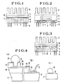
- In recent years, high-density high integration semiconductor integrated circuits have been developed. Correspondingly, an LSI chip to be used has been remarkably large-scaled. Also, its heat density has been increasingly enhanced. To deal with such a situation, there has been widely used pin-grit-array package in which a great number of terminals for outer connection are arranged in a matrix shape on one surface of a package substrate.
- A general structure of the pin-grit array is roughly classified in two types, i.e. "cavity-up" type and "cavity-down" type in view of manner of incorporating a chip. The cavity-up type is a structure as shown in Fig. 2 in which a chip carrier incorporating the chip looks up. The cavity-down type is a structure as shown in Fig. 3 in which a chip carrier incorporating the chip looks down.
- Referring to Fig. 2, the structure of the cavity-up type package will be explained below. A
chip 1 is fixedly attached to aninsulating base substrate 6 through afixing layer 3. Electric connection is made from thechip 1 to electrode part (not shown) on theinsulating base substrate 6 throughe.g. wire bondings 2, and further to pin-like terminals 5 for outer connection throughconductive layers 4 in theinsulating base substrate 6. Although in Fig. 2, wirings are extended in the substrate using a multi-layer plate as the insulating base substrate, they may also be extended by means of thin films and the like provided on theinsulating base substrate 6 so as to be connected with theouter connection terminals 5 through conductive parts vertically provided within theinsulating base substrate 6. Airtightness of the package is important from the viewpoint of reliability in the correct operation of the LSI chip, etc. In order to assure the airtightness of the package, theinsulating base substrate 6 on which the chip is mounted is sealed by aninsulating cap substrate 8 using e.g. soldering so as to be shut out from outer environment. In the package having such a structure as mentioned above, heat generated in thechip 1 propagates to theinsulating base substrate 6 through thechip fixing layer 3. The package is inserted and fixed onto a printed board through the outerconnection terminal pins 5. In this case, the distance between thebase substrate 6 and the printed board is as short as several millimeters. Thus, compulsory cooling from below the base substrate provides only slight effect. Accordingly, heat spreads in theinsulating base substrate 6 and propagates to the insulatingcap substrate 8 via apackage sealing layer 7. And the heat propagates to afin 9 fixed to theinsulating base substrate 6 and is radiated therefrom. - Explanation will be given for the structure of the cavity-down type package of Fig. 3. The
chip 1 is fixedly attached to theinsulating base substrate 6. Electric connection is made from thechip 1 to electric part (not shown) on the insulatingcap substrate 8 throughe.g. wire bondings 2, and further to the pin-like terminals 5 for outer connection through theconductive layers 4 in theinsulating cap substrate 6. In order to assure the airtightness of the package, theinsulating cap substrate 8 incorporating theconductive layers 4 is sealed by a sealingcap 12 using e.g. soldering. In the package having such a structure, heat generated in thechip 1 propagates to theinsulating base substrate 6 throughchip fixing layer 3. And the heat spreads in theinsulating base substrate 6 and propagates to thefin 9 fixed thereto thereby to be radiated therefrom. - In recent years, there has been proposed a structure in which a multi-layer is not used in the insulating cap substrate to extend the wirings, as disclosed in JP-A-62-106635. In this structure, the wirings are extended on the insulating base substrate on which the chip is mounted and outer connection terminal pins are provided on the ends of the wirings. An insulating cap substrate having a large number of through-holes is also prepared. The outer connection terminal pins on the insulating base substrate are fit into the through-holes of the insulating cap substrate. And the insulating base substrate is sealed in its periphery and also the through-holes through which the outer connection terminal pins are passed are sealed with soldering, resin, etc.
- Further, there is proposed in JP-A-62-9649 a structure in which a wiring layer is formed in the substrate on which a semiconductor chip is mounted and a cap for sealing the semiconductor chip traverses the wiring layer. In this structure, the wiring layer is partially sealed by the cap but not entirely covered with the cap so that it must be covered with other means.
- The semiconductor device package structures as mentioned above have the following problems to be solved.
- The cavity-up type structure has a defect of a long heat propagation path. Heat generated in the chip must pass the long heat propagation path consisting of the
chip fixing layer 3, theinsulating base substrate 6, thepackage sealing layer 7, theinsulating cap substrate 8 and thefin 9. Thus, the cavity-up type package structure is poor in its cooling efficiency and large in its heat resistance. This make it difficult to incorporate, in the package structure, a chip which has been very highly densified or integrated in recent years to have a high heat generation density. - On the other hand, in the cavity-down type package structure as shown in Fig. 3, heat generated in the chip is radiated via the
chip fixing layer 3, theinsulating base substrate 6 and thefin 9. Thus, the heat propagation path consisting of the sealing layer and the cap is omitted so that the heat propagation path in the cavity-down structure is shorter than that in the cavity-up structure. Therefore, the cavity-down structure is more advantageous than the cavity-up structure with respect to their cooling efficiency. - However, the cavity-down package structure also has the following disadvantages.
- First, the cavity-down structure becomes complicate in its structure. Since the chip looks down, the electric connection from the chip to the outer
connection terminal pins 5 is more complicate than the cavity-up structure. Also, since the chip and the outer connection terminals are located on the same side, it is difficult to make the wire bonding, which requires some particular contrivance in assembling the package. Further, since in view of the structure, the wire bonding is made directly from the chip onto the cap substrate, in order to extend the wiring, the cap substrate must be constructed in a multi-layer structure. Moreover, since the outerconnection terminal pins 5 can not be provided on thecap 12 for holding the airtightness of the package, the area where the outer connection terminal pins can be arranged is smaller than the cavity-down package structure. - Secondly, the cavity-down structure provides reduced transmission speed due to its complicate structure. The transmission speed is reduced as the permittivity is increased. Thus, the conventional cavity-down structure, which travels a relatively long path of ceramic that has a larger permittivity than plastic, is inferior to the cavity-up structure in their transmission characteristic. Therefore, the conventional cavity-down structure can not sufficiently satisfy the demand of high speed increasing in recent years.
- The cavity-down structure proposed in the above JP-A-62-106635, which is seemed to provide the transmission speed substantially equal to the cavity-up structure, has disadvantages of complicated steps of passing the outer connection terminal pins through the through-holes and thereafter sealing the through-holes. Further, the structure proposed in the above JP-A-62-9649 has a problem that the wiring layer is not entirely covered with the cap.
- One object of the present invention is to provide a package for a semiconductor device which is free from the above problems, permits a chip producing a large amount of heat to be mounted and has a high transmission speed characteristic.
- Another object of the present invention is to provide a ceramic cap for a semiconductor package which can hermetically seal a semiconductor device and permits outer connection terminals to be provided.
- Still another object of the present invention is to provide a substrate for a semiconductor package which can reduce a propagation delay-time.
- A further object of the present invention is to provide a computer which can perform a high speed processing.
- In order to attain the above one object, in accordance with the present invention, there is provided a package for a semiconductor device (referred to as a semiconductor package) comprising a insulating base substrate on which a semiconductor device is mounted and an insulating cap substrate with plural outer connection terminals on its one surface and with electrodes provided on conductive layers for electric connection on its inner surface wherein electrodes on the insulating base substrate and electrodes on the insulating cap substrate are connected with each other by means of conductive material such as bumps.
- Further, there is provided a semiconductor package comprising an insulating substrate on which a semiconductor device is mounted and wiring layers are provided, and an insulating cap for hermetically sealing the semiconductor device and the wiring layers from the open air, wherein said wiring layers have electrodes to be connected with outer connection terminals and a plurality columns of the electrodes are arranged regularly in the entire outer periphery of the semiconductor device.
- Moreover, there is provided a semiconductor package comprising a wiring layer having plural conductive layers with different lengths regularly arranged wherein a plurality of columns of these plural conductive layers are arranged regularly or an insulating cap has outer connection terminals on its outer surface which are connected with outer connection pins.
- In order to attain the above another object of the present invention, there is provided a ceramic cap for a semiconductor package, made of sinter, for sealing a semiconductor device, wherein the cap has conductive layers formed in through-holes by conductive paste. In addition to the conductive layers, the cap has outer connection pins connected with outer connection terminals of the conductive layers.
- In order to attain the above still another object of the present invention, there is provided a substrate for a semiconductor package, made of sintered ceramic, on which a semiconductor device is mounted, wherein the substrate has plural wiring layers with different wiring lengths regularly arranged at regular intervals and a plurality of columns of these plural wiring layers are arranged regularly. Further, there is provided a substrate for a semiconductor package, wherein the substrate has wiring layers, the wiring layers have electrodes to be connected with outer connection terminals and a plurality of columns of the electrodes are arranged regularly on the entire outer periphery of the semiconductor device. Moreover, there is provided a substrate for a semiconductor package, wherein wiring layers are provided on a resin layer the wiring layers have electrodes to be connected with outer connection terminals and a plurality of columns of the electrodes are arranged regularly on the entire outer periphery of the semiconductor device.
- In order to attain the above further object of the present invention, there is provided a computer comprising a platter, a multi-layer printed circuit board and a semiconductor package for logic and another semiconductor package for main storage which are mounted on the circuit board, wherein at least one of the semiconductor packages has an insulating substrate on which a semiconductor device is mounted and wiring layers are provided and an insulating cap for hermetically sealing the semiconductor device and the wiring layers from the open air; the cap has, on its outer surface, outer connection terminals and, on its internal surface, electrodes provided on conductive layers electrically connected with the outer connection terminals; and electrodes of said wiring layers are connected with the electrodes on the internal surface of the cap by means of conductive material.
- In accordance with the present invention, in a semiconductor package comprising an insulating base substrate on which a semiconductor device is mounted and an insulating cap substrate with plural outer connection terminals on its one surface and with electrodes provided on conductive layers for electric connection on its inner surface, electrodes on the insulating base substrate and electrodes on the insulating cap substrate are connected with each other by means of conductive material such as bumps. Thus, although it is a cavity-down structure, it is possible to adopt the insulating cap substrate in such a simple structure as conductive layers are provided vertically to the cap substrate. Further, the insulating cap substrate need not be in a multi-layer. Thus, if the cap substrate is made of material having a large permittivity such as ceramic, the propagation path therethrough is limited to the minimum, thereby permitting delay of the propagation time to be minimized. Moreover, in a manufacturing process, the insulating cap substrate previously provided with outer connection terminal pins is aligned in the ordinary manner to be connected with the insulating base layer. Therefore, the present invention can be realized with the same operability as in the cavity-up type structure.
- As a connection method using a solder bump, the CCB (controlled collapse bonding) is proposed in U.S. Patent No. 3429040. This method permits the connection to be made in a ball shape held in a certain size so that fused solder does not flows out.
- Again, in accordance with the present invention, in a semiconductor package comprising an insulating base substrate on which a semiconductor device is mounted and an insulating cap substrate with plural outer connection terminals on its one surface and with electrodes provided on conductive layers for electric connection on its inner surface, electrodes on the insulating base substrate and electrodes on the insulating cap substrate ae connected with each other by means of conductive material. Therefore, the semiconductor package of the present invention provides as excellent heat radiating property, and also provides improved transmission characteristic since the structure of the insulating cap substrate is simplified to decrease the distance travelling a path having a comparatively large permittivity thereby to reduce the propagation delay time. Further, if the cap substrate and the base substrate are made of the seam material, a semiconductor package with high reliability is obtained.
- Further, the ceramic cap for a semiconductor package in accordance with the present invention permits a semiconductor device to be sealed and outer connection terminals to be provided.
- Moreover, the substrate for a semiconductor package in accordance with the present invention, because of the absence of a ceramic multi-layer plate, permits wirings to be formed on its ceramic surface so as to shorten the length of the wiring layers, thereby reducing the delay time.
- Furthermore, if passive elements are incorporated in the cap substrate, abrupt voltage variation in the neighborhood of a semiconductor device chip can be reduced and also the wiring length of the circuit can be made smaller than the conventional structure in which capacitors are connected externally of the package. Thus, in accordance with the present invention, the quality of the transmission waveform can be improved and the transmission time can be reduced.
- Finally, the computer in accordance with the present invention permits a higher speed processing to be performed because of reduced propagation delay time and a high efficiency processing to be performed in bank terminals in which intermediate computers are used.
-
- Fig. 1 is a sectional view of one embodiment of a semiconductor package in accordance with the present invention;
- Figs. 2 and 3 are a sectional view of the prior art semiconductor package, respectively;
- Figs. 4a, 4b and 4c are a sectional view showing the details of electrode part of the semiconductor package of the present invention, of wire-bonding part thereof and sealing part thereof, respectively;
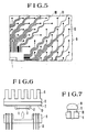
- Fig. 5 is a plan view of the pattern of wiring layers formed on a base substrate;
- Fig. 6 is a sectional view of the other package structure in accordance with the present invention;
- Fig. 7 is a sectional view of the pin connection part in Fig. 6;
- Fig. 8 is a sectional view of a semiconductor package incorporating semiconductor devices in accordance with the present invention;
- Fig. 9 is a plan view of the electrode part in Fig. 8;
- Fig. 10 is a sectional view of a semiconductor package in accordance with the present invention in which plural semiconductor devices are mounted on one substrate;
- Fig. 11 is a perspective view of a computer in which the semiconductor package of the present invention is incorporated; and
- Figs 12 and 13 are a sectional view of a semiconductor package in accordance with the present invention in which passive elements are formed in a sealing cap, respectively.
- The present invention will be explained in connection with several embodiments shown in the drawings.
- Fig. 1 is a sectional view of a first embodiment of the semiconductor package in accordance with the present invention. As seen from Fig. 1, the semiconductor package of the first embodiment is constructed in a cavity-down structure. In Fig. 1, a
chip 1 is fixedly attached to an insulatingbase substrate 6. The insulatingbase substrate 6 and aninsulating cap substrate 8 are made of sinter of aluminum nitride (AlN). The thermal expansion coefficient of AlN, which is 3.4 x 10⁻⁶/°C, is nearly equal to that of silicon which is a material of thechip 1. Therefore, thesubstrate chip 1 with high reliability. The thermal conduction coefficient of AlN is as comparatively large as 150 w/m·k. Thus, the heat generated in thechip 1 can be sufficiently conducted to afin 9 which is made of metal such as Al, high thermal conductivity ceramic, etc. - Incidentally, the insulating
base substrate 6 may be made of sinter of silicon carbide (SiC) having high thermal conductivity in place of AlN. The thermal expansion coefficient of the high thermal conductivity SiC sinter, which is 3.7 x 10⁻⁶/°C, is nearly equal to that of silicon which is a material of thechip 1 so that the SiC sinter can be connected with thechip 1 with high reliability. And the thermal conduction coefficient thereof is as high as 20 w/m·k, which reduces the heat resistance of the package. The other materials may also be employed as long as they are an insulating material having a thermal expansion coefficient nearly equal to silicon and a sufficiently high thermal conduction coefficient. - The insulating
cap substrate 8 has through-holeconductive layers 4 and outer connection terminal pins 5 fixed thereonto; the through-holeconductive layers 4 are formed by making through-holes in a green sheet of AlN powder compound, injecting paste tungsten into the through-holes and also baking them; and the outer connection terminal pins 5 are made of Koval. An alumina (Al₂O₃) sinter, in which conductive part can be formed, can be employed in place of the above AlN powder compound. - In view of reliability in the airtightness of the package, it is desired that the insulating
base substrate 6 and the insulatingcap substrate 8 have nearly equal thermal expansion coefficients. A combination thereof which provides the highest reliability in the airtightness of the package among the materials mentioned above is that of the insulatingbase substrate 6 and the insulatingcap substrate 8 both of which are made of AlN. - The electric connection of the package is made in the following manner. The
chip 1 is connected with wiring electrode part (not shown) on the insulatingbase substrate 6 by means ofwire bondings 2, etc. The electric connection is made through wiring extension layers 10 and further from the electrodes at the terminals of the wiring layers 10 on the insulating base substrate to electrodepart 11 of the insulatingcap substrate 8 through solder bumps. Further, the electric connection continues to pin-likeouter connection terminals 5 through through-hole connection layers 4 within the insulatingcap substrate 8 which are formed vertically to thebase substrate 6. In order to assure the airtightness of the package, the insulatingcap substrate 8 incorporating theconductive layers 4 is fixed to the insulatingbase substrate 6 by apackage sealing layer 7 at their peripheral position. - The
conductive layers 4 in the insulatingcap substrate 8 communicate its front surface with its back surface at the shortest distance so that the propagation delay time can be minimized even if thesubstrate 8 is made of ceramic having a comparatively large permittivity. - The wiring layers 10 are in the following structure. A resin film such as polyimide is formed on an aluminum nitride (AlN) substrate. Aluminum thin films formed on the resin film connect the connection electrodes for the
wire bondings 2 at their terminals with theelectrodes 11 of the insulatingcap substrate 8 for theconductive layers 4. Aluminum used as the wiring material makes low the electric resistance of the package. The wiring material may be, instead of aluminum, any metal having high conductivity such as gold (Au), silver (Ag), copper (Cu), etc. - Figs. 4a, 4b and 4c are sectional views of the details of the electrode, wire bonding part and sealing part of the package of Fig. 1. A
resin layer 14 is formed at the areas other than the electrodes, and a depositedfilm 13 of titanium (Ti) - platinum (Pt) - gold (Au) is formed on the electrode. As mentioned above, thewiring layer 10 in this embodiment is formed on theresin film 14 having a small permittivity so that the propagation delay time is short. Theresin layer 14 is made of polyimide system resin. The permittivity of this layer is 3.5 or less, preferably 3 or less. As long as the surface of the insulatingbase substrate 6 has sufficient smoothness, the depositedfilm 13 may be formed for wiring without providing theresin film 14. - A
solder 12 in a ball shape is formed on the depositedfilm 13. Thissolder 12 can be provided by melting solder embedded in gap portion of a heat-resistant substrate having poor wettability for solder so as to be transferred thereto. Thus, by using the gap portion corresponding to the portion where the solder is provided on the base substrate, thesolder 12 can be formed at a predetermined position. The size of thesolder 12 can be changed by controlling the thickness of the heat-resistant substrate. - The
solder 12 is previously provided on thebase substrate 6 or the cap substrate. Thebase substrate 6 and thecap substrate 8 are aligned to each other and bonded by the sealingsolder 7. - Fig. 5 is a plan view partially showing the pattern of the
wiring layer 10 on the insulatingbase substrate 6. In this embodiment, 400 wiring layers are arranged to provide the same pattern at each of four sides of the region where thechip 1 is mounted. A plurality of columns or groups of the wiring layers are arranged; each group consists of regularly arranged plural wiring layers having different wiring lengths. Also, 400electrodes 11 are arranged in seven columns - In the package in the structure mentioned above, heat generated in the
chip 1 conducts to the insulatingbase substrate 6 of AlN through thechip fixing layer 3. The heat disperses in thesubstrate 6 and conducts to thefin 9 bonded to thesubstrate 6 thereby to be radiated therefrom. The path of heat conduction is so short that the package of this embodiment is suitable to mount a bipolar ECL chip consuming a large electric power, etc. - The outer connection terminal pins 5 are made of Koval (an alloy of Fe-29 Ni-17 Co). The thermal expansion coefficient of Koval, which is 4.5 x 10⁻⁶/°C, is nearly equal to that of AlN. Thus, all the components of the package in this embodiment have a thermal expansion coefficient nearly equal to that of silicon so that thermal fatigue due to differences among the thermal expansion coefficients of the members of the package does not occur anywhere in the package.
- As mentioned above, the insulating
cap substrate 8 is prepared by making through-holes in a green sheet of a sinter mainly of AlN, injecting paste of powder of tungsten, molybdenum, etc. in the through-holes and baking the green sheet. The through-holes are formed at the areas corresponding to theelectrodes 11 provided int he capsubstrate 8. Formed at these area are deposited films having high solder-wettability and also formed at the sealing parts are deposited films. Further,solder 12 is bonded onto these deposited films. Prior to sealing thecap substrate 8, thepin 5 mentioned above are connected to thecap substrate 8 by breezing, etc. at the temperature where the breasing metal is not melted at the subsequent sealing temperature. - The
cap substrate 8 is fixed to thebase substrate 6 so that thechip 1 and the wiring layers 10 are protected from the open air in such a manner that the electrodes and the upper portion of thechip 1 are made integral. - The
chip 1 and theelectrodes 11 of thebase substrate 6 are wire-bonded. Thewirings 2 may be metallic wires having a high conductivity such as Au, Al, Cu, etc. Thewirings 2 may have a diameter of 100 µm or less, preferably 30 - 50 µm. Ball bonding (the tip is ball-shaped) is made for thechip 1 while wedge bonding is made for the electrodes. These bondings are performed through pressure-welding by ultrasonic vibration. - Although in this embodiment, the
base substrate 6 and thecap substrate 8 are sealed by asingle sealing part 7, they may be sealed by double or triple sealing parts whereby the airtightness of the package can be further improved. - The package in this embodiment may be fabricated in the following process. The
chip 1 is mounted on the insulatingbase substrate 6. The wiring layers 10, the sealingsolder 7 andsolder 12 for connection of theelectrodes 11 are formed. Thereafter, thechip 1 and the wiring layers are connected with each other by thewirings 2. The insulatingcap substrate 8 on which the pins for connection of outer terminals are previously provided is connected with the wiring layers 10. The sealingsolder 7 and the solder at the electrode parts may be provided in the insulatingcap substrate 8. Since these solders have different sizes, it is desired that the sealingsolder 7 is provided in one of both substrate while theelectrode part solder 12 is provided in the other thereof. The coolingfin 9 may be bonded to thebase substrate 6 using resin bonding agent, solder, etc. after the package has been assembled. - Fig. 6 is a sectional view of a package of a second embodiment of the present invention. This embodiment also is a cavity-down type package structure like the first embodiment. The insulating
base substrate 6 and the insulatingcap substrate 8 are made of a sinter of silicon carbide (SiC) having high thermal conductivity containing BeO of 2% or less by weight. Thechip 1 is fixed to the insulatingbase substrate 6. The structure on the insulatingbase substrate 6 side is the same as the first embodiment. The insulatingcap substrate 8 must be provided with conductive layers within it. Then, if SiC having high thermal conductivity is to be used as a material of the insulatingcap substrate 8, the sintering temperature is too high so that conductive layers can not be provided within the sinter. In order to solve this problem, in accordance with this embodiment, the insulatingcap substrate 8 having the following structure is proposed. Through-holes are provided at the portions corresponding to the electrodes at the wiring terminals on the insulatingcap substrate 8. Thepins 5 each with a T-shape head to both (front and back) surfaces of which a brazing material such as solder is applied is passed through the through-holes and fixed as seen from Fig. 7 which shows an enlarged view of a part of the pin fixing portion. As in the first embodiment, the insulatingcap substrate 8 having such a structure is fixed to the insulatingbase substrate 6 in such a manner that the brazing material applied to the heads of thepins 5 is fixed to the electrodes on the insulatingbase substrate 6 together with their periphery. In this way, by inserting the conductive material such as a breasing material, bump, etc. between the insulatingbase substrate 6 and the insulatingcap substrate 8, the structure of the insulating cap substrate can be simplified and the sinter of SiC having a high thermal conductivity, which can not be multi-layered, can be adopted as a material of thecap substrate 8. The thermal conduction coefficient of SiC having a high thermal conductivity is twice as large as aluminum nitride (AlN), thereby providing good heat resistance to the package. Further, since bothsubstrates - Also in this embodiment, the wiring layers 10, the sealing part, the electrodes and the wire bonding parts for the insulating
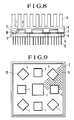
base substrate 6 can be formed in the same manner as in the first embodiment. Thefin 9 made of metal can also be provided in the same manner. - Fig. 8 shows a sectional view of a third embodiment of the present invention. Fig. 9 is a plan view of the insulating
base substrate 6 viewed from the chip side before theinsulating cap substrate 8 is provided. The package of this embodiment is also in a cavity-down type structure. - Nine (9) chips 1 (including some small-sized chips and some large-sized chips) are fixed to the insulating
base substrate 6. In accordance with the use of the package, the number of the chips may be increased or some chips may exchanged. Fig. 9 shows the insulatingbase substrate 6 on which a CPU is centrally mounted and memories are mounted in the periphery. - The insulating
base substrate 6 and the insulatingcap substrate 8 are made of sinter of aluminum nitride (AlN). By baking a green sheet of a plate made of AlN powder and another green sheet having openings where the chips are to be mounted in such a state that they are stacked, the insulatingbase substrate 6 having recesses where the chips are to be mounted is prepared. Thechips 1 are mounted in the recesses, and the electrodes on the side of each chip and those of the wiring layers 10 of the base substrate around the chip are connected with each other by means offilm carriers 2. The reason why thefilm carriers 2 are employed is that since the insulatingcap substrate 8 is constructed as a sheet considering kinetic property relative to the large-scaling of the package, the gap between bothsubstrates - The wiring structure for electric connection starting from the electrodes at the terminals of the wiring layers 10 on the base substrate around the
chips 1 is the same as that in the first embodiment. The electric connection is made through the wiring layers 10 (the wiring pattern is not shown) and further made from the electrodes at the terminals of the wiring layers on the insulatingbase substrate 6 to the electrodes in the insulating cap substrate through the solder bumps 11 at the areas of connecting both substrate. The electric connection continues to outer connection terminal pins 5 via theconductive layers 4 formed in the insulatingcap substrate 8 which are vertical to thebase substrate 6. The solder bumps 11 are provided on the entire surface of thebase substrate 6 other than the areas of the chips 1 (although not shown). - The insulating
cap substrate 8 is prepared in the same manner as in thefirst embodiment 1. Namely, the insulatingcap substrate 8 is prepared by baking a green sheet of AlN together with paste of tungsten injected into the through-holes provided in the green sheet and fixing outer connection terminal pins 5 to the through-hole conductive layers. - The air tightness of the package can be improved since the insulating
base substrate 6 and the insulatingcap substrate 8 are made of the same material. Theconductive layers 4 in the insulatingcap substrate 8 communicate its front surface with its back surface at the shortest distance so that the propagation delay time can be minimized even if thesubstrate 8 is made of ceramic having a comparative large permittivity. - The wiring layers 10 are provided in the same construction as those in the first embodiment. In the case where a plurality of chips are incorporated in one package as in this embodiment, signal communication is performed also among the chips through wirings. Thus, the wiring pattern to be used is made complicate. However, in accordance this embodiment, if the wiring pattern design is to be changed, it can be performed only by changing the wiring pattern without changing the insulating
base substrate 6 and the insulatingcap substrate 8, so that the wiring pattern can be easily designed. - The solder bumps 11 are commonly used for each
wiring layer 10 from eachchip 1. Thus, the wiring structure is such that the solder bumps 11 necessary for each chip are not provided individually but commonly used for each chip. - In the package having the structure mentioned above, heat generated in the chips 21 propagate to the insulating
base substrate 6 of AlN through the corresponding fixing layers 3. The heat spreads in the insulatingbase substrate 6 and propagates to thefin 9 so as to be radiated therefrom. In this way, the heat conduction path is so short that the cooling efficiency of the package is improved. Thus, it is possible to incorporate some chips having low heat resistance and some chips producing a large amount of heat in the same package. Therefore, the package of this embodiment has an improved operation processing capability as compared with the combination of the packages in each of which a single chip is incorporated. - Fig. 10 is a sectional view of a package in which a plurality of chips are incorporated. This embodiment is different from the third embodiment in that the insulating
base substrate 6 is in the shape of a plate and wire bondings are made between thechips 1 and the wiring layers 10 as in the first embodiment. The plan structure is as shown in Fig. 9 in which 9 (nine) chips are arranged in such a way that one CPU chip is centrally arranged and the remaining eight memory chips are arranged in the periphery. Also in this embodiment, the wiring pattern can be made so that the solder bumps necessary for each chip can be commonly used. A cooling fin (not 8 shown) may be also provided. - Also in this embodiment, the
conductive layers 4 are provided in thecap substrate 8 at the shortest distance so that the signal propagation delay time is reduced and the high speed operation can be realized. - Fig. 11 is a perspective view of a super computer in which the semiconductor packages of the present invention are packaged. The semiconductor packages in accordance with the first to the fourth embodiment are three-dimensionally mounted in a multi-layer printed
boards 15 and connected with platters by means of connectors. The platter structure is constituted by two stages of an upper platter and lower platter from the bottom of which cooling air is supplied. A cross-free-grid 16 is provided between both platters so as to eliminate temperature dispersion due to the cooling. - The semiconductor packages including a package for logic, a package for VR (vector register), a package for main storage, and a package for extension storage are packaged in highly integrated logic platters. The package for logic incorporates a logic LSI chip or RAM module; the package for VR incorporates a logic LSI chip or VRLSI chip; the package for main stage incorporates a MS (main storage) module; and the package for extension storage incorporates a DRAM (dynamic random access memory). These packages are packaged in a printed board by means of the techniques of surface packaging, axial packaging, both-surface-packaging, etc. This embodiment permits a super computer of the highest speed to be realized.
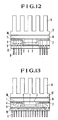
- Fig. 12 is a sectional view of the cavity-down type package structure in accordance with the present invention. In Fig. 12, a
chip 1 is fixedly attached to an insulatingbase substrate 6. The insulatingbase substrate 6 is made of a sinter of aluminum nitride (AlN). The insulatingcap substrate 8 is made of glass ceramic. The thermal expansion coefficient of AlN, which is 3.4 x 10⁻⁶/°C, is nearly equal to that silicon which is a material of thechip 1. Therefore, thebase substrate 6 can be connected with the chip with high reliability. Also the thermal conduction coefficient of AlN is as comparatively large as 150 w/m·k. Thus, the heat generated in thechip 1 can be sufficiently conducted to afin 9 through afin bonding layer 17. - Incidentally, the insulating
base substrate 6 may be of sinter of silicon carbide (SiC) containing Be or BN, which has a high thermal conductivity, in place of AlN. The thermal expansion coefficient of the high thermal conductivity SiC, which is 3.7 x 10⁻⁶/°C, is nearly equal to that of silicon which is a material so that the SiC sinter can be connected with thechip 1 with high reliability. And the thermal conduction coefficient thereof is as high as 270 w/m·k, which reduces the heat resistance of the package. The other materials may also be employed as long as they are an insulating material having a thermal expansion coefficient nearly equal to silicon and a sufficiently high thermal conduction coefficient. - The insulating
cap substrate 8 of glass ceramic is a multi-layer substrate incorporating passive elements such as capacitors, resistors, inductances, etc. The insulatingcap substrate 8 is prepared by forming through-holes in a green sheet of glass ceramic, baking the green sheet together with conductive material (e.g. Au, Ag, Cu) injected into the through-holes so as to provide conductive layers and fixing outer connection terminal pins of Koval to the conductive layers. Any other material, which permits passive elements and conductive layers to be provided in the cap substrate, can be employed in place of the above glass ceramic. - In view of reliability in the airtightness of the package, it is desired that the insulating
base substrate 6 and the insulatingcap substrate 8 have nearly equal thermal expansion coefficients. A combination thereof which provides the highest reliability in the airtightness of the package among the materials mentioned above is that of the insulatingbase substrate 6 of AlN as in the first embodiment and the insulatingcap substrate 8 of glass ceramic containing borosilicate glass, which has a thermal expansion coefficient near to that of AlN. - The electric connection of the package is made in the following manner. The
chip 1 is connected with the electrodes (not shown) on the insulatingbase substrate 6 by means ofwire bondings 2, TAB (Tape Automated bonding), or the like. The electric connection is made through wiring extension layers 10 and further from the electrodes at the wiring terminals on the insulatingbase substrate 6 to electrodes of the insulatingcap substrate 8 through the solder bumps 11. Further, the electric connection continues to pin-likeouter connection terminals 5 through theconductive layers 4 within the insulatingcap substrate 8 which are formed vertically to thebase substrate 6. Thecapacitors 14 are connected with theconductive layers 4 in parallel to chip power supply terminal layers and ground layers. Thecapacitors 14, which are incorporated in thecap substrate 8, can reduced abrupt voltage variation in the neighborhood of thechip 1 and also shorten the wiring length of the circuit as compared with capacitors provided externally of the package. Thus, the quality of the transmission waveform can be improved and the transmission time can be reduced. - In order to assure the airtightness of the package, the insulating
cap substrate 8 incorporating theconductive layers 4 is fixed to the insulatingbase substrate 6 by apackage sealing layer 7 at the peripheral position. - The
conductive layers 4 in the insulatingcap substrate 8 communicate its front surface with its back surface so that the propagation delay time can be minimized even if thecap substrate 8 is made of ceramic having a comparatively large permittivity. - The
wiring extension layer 10 is in the same structure as the first embodiment. - In the package in the structure mentioned above, heat generated in the
chip 1 conducts to the insulatingbase substrate 6 of AlN through thechip fixing layer 3. The heat disperses in thesubstrate 6 and conducts to thefin 9, which is bonded to thesubstrate 6 through afin bonding layer 13 made of high thermal conductivity resin, etc., thereby to be radiated therefrom. The path of heat conduction is so short that the package of this embodiment is suitable to mount a bipolar ECL chip consuming a large electric power, etc. - The outer connection terminal pins 5 are made of Koval (an alloy of Fe-29 Ni-17 Co). The thermal expansion coefficient of Koval, which is 4.5, is nearly equal to that of glass ceramic. Thus, all the components of the package in this embodiment have a thermal expansion coefficient nearly equal to that of silicon so that thermal fatigue due to differences among the thermal expansion coefficients of the members of the package does not occur anywhere in the package.
- Fig. 13 is a sectional view of a cavity-down type package of the present invention. The insulating
base substrate 6 has the same structure and is made of the same material as in the first embodiment. The size of the chip is increased as the number of terminals from thechip 1 is increased. Then, in accordance with this embodiment, in order for the outer connection terminals to be also provided at the area of the insulatingcap substrate 8 which is located immediately below thechip 1, the insulatingcap substrate 8 incorporates passive elements and theconductive layers 4 are multi-layer-wired. Thus, even if the number of terminals from thechip 1 is increased, the outer connection terminals can be provided onto the entire outer surface of the insulatingcap substrate 8 so that the size of the package can be minimized.
Claims (10)
an insulating base substrate (6) on which a semiconductor device (1) is mounted and wiring layers (10) are provided;
an insulating cap substrate (8) for sealing said semiconductor device (1) and the wiring layers (10) so as to be protected from the open air;
terminals (5) for outer connection provided on the outer surface of said insulating cap substrate (8);
electrodes (11) provided on the inner surface of said insulating cap substrate (8), which are electrically connected with said terminals (5) for outer connection; and
conductive members for connecting electrodes of said wiring layers (10) with said electrodes (11) provided on the inner surface of said cap substrate (8).
an insulating base substrate (6) on which a semiconductor device (1) is mounted and wiring layers (10) are provided;
an insulating cap substrate (8) for sealing said semiconductor device (1) and the wiring layers (10) so as to be protected from the open air; and
electrodes (11) provided to said wiring layers (10) so as to be connected with terminals (5) for outer connection, a plurality of columns of said electrodes (11) being regularly arranged in the entire outer periphery of said semiconductor device (1).
an insulating base substrate (6) on which a semiconductor device (1) is mounted and wiring layers (10) are provided;
an insulating cap substrate (8) for sealing said semiconductor device (1) and said wiring layers (10) so as to be protected from the open air; and
said wiring layers (10) being arranged with different lengths and at regular intervals, a plurality of columns thereof being regularly arranged.
an insulating base substrate (6) on which a semiconductor device (1) is mounted and wiring layers (10) are provided ;
an insulating cap substrate (8) for sealing said semiconductor device (1) and the wiring layers (10) so as to be protected from the open air; and
outer connection pins (5) bonded to outer connection terminals which are formed on the outer surface of said insulating cap (8).
conductive layers (4) formed using conductive paste in through-holes provided within said ceramic cap (8).
conductive layers (4) formed using conductive paste in through-holes provided within said ceramic cap (8); and
outer connection pins (5) connected with outer connection terminals of said conductive layers (4).
a plurality of wiring layers (10) arranged with different lengths and at regular intervals, a plurality of columns thereof being regularly arranged.
wiring layers (10); and
electrodes (11) provided on the wiring layers (10) so as to be connected with outer connection terminals (5), a plurality of columns thereof being arranged regularly in the entire outer periphery of the area where said semiconductor chip (1) is mounted.
a platter;
a multi-layer printed board (15) mounted on said platter through a connector;
a semiconductor package for logic and a semiconductor package for main storage which are mounted on said printed board (15); and
at least one of said semiconductor package comprising:
an insulating base substrate (6) on which a semiconductor device (1) is mounted and wiring layers (10) are provided;
an insulating cap substrate (8) for sealing said semiconductor device (1) and the wiring layers (10) as as to be protected from the open air,
terminals (5) for outer connection provided on the outer surface of said insulating cap substrate (8),
electrodes (11) provided on the inner surface of said insulating cap substrate (8), which are electrically connected with said terminals (5) for outer connection, and
conductive members for connecting electrodes of said wiring layers (10) with said electrodes (11) provided on the inner surface of said cap substrate (8).
Applications Claiming Priority (2)
| Application Number | Priority Date | Filing Date | Title |
|---|---|---|---|
| JP81258/88 | 1988-04-04 | ||
| JP8125888A JPH0756887B2 (en) | 1988-04-04 | 1988-04-04 | Semiconductor package and computer using the same |
Publications (3)
| Publication Number | Publication Date |
|---|---|
| EP0336359A2 true EP0336359A2 (en) | 1989-10-11 |
| EP0336359A3 EP0336359A3 (en) | 1991-03-20 |
| EP0336359B1 EP0336359B1 (en) | 1995-01-25 |
Family
ID=13741349
Family Applications (1)
| Application Number | Title | Priority Date | Filing Date |
|---|---|---|---|
| EP19890105868 Expired - Lifetime EP0336359B1 (en) | 1988-04-04 | 1989-04-04 | Semiconductor package |
Country Status (4)
| Country | Link |
|---|---|
| US (1) | US5097318A (en) |
| EP (1) | EP0336359B1 (en) |
| JP (1) | JPH0756887B2 (en) |
| DE (1) | DE68920767T2 (en) |
Cited By (6)
| Publication number | Priority date | Publication date | Assignee | Title |
|---|---|---|---|---|
| EP0620594A2 (en) * | 1993-04-13 | 1994-10-19 | Shinko Electric Industries Co. Ltd. | Semiconductor device having mounting terminals |
| US5420460A (en) * | 1993-08-05 | 1995-05-30 | Vlsi Technology, Inc. | Thin cavity down ball grid array package based on wirebond technology |
| EP0662245A1 (en) * | 1992-09-16 | 1995-07-12 | CLAYTON, James E. | A thin multichip module |
| FR2721437A1 (en) * | 1994-06-17 | 1995-12-22 | Xeram N | Hermetic casing with improved heat dissipation for encapsulating electronic components |
| GB2326454A (en) * | 1997-06-21 | 1998-12-23 | Conveyor Units Ltd | A clutch for a live roller conveyor section |
| US6349870B1 (en) * | 1999-04-12 | 2002-02-26 | Murata Manufacturing Co., Ltd | Method of manufacturing electronic component |
Families Citing this family (43)
| Publication number | Priority date | Publication date | Assignee | Title |
|---|---|---|---|---|
| US20010030370A1 (en) * | 1990-09-24 | 2001-10-18 | Khandros Igor Y. | Microelectronic assembly having encapsulated wire bonding leads |
| JP2730304B2 (en) * | 1991-03-13 | 1998-03-25 | 日本電気株式会社 | Semiconductor device |
| US5199164A (en) * | 1991-03-30 | 1993-04-06 | Samsung Electronics Co., Ltd. | Method of manufacturing semiconductor package |
| EP0544329A3 (en) * | 1991-11-28 | 1993-09-01 | Kabushiki Kaisha Toshiba | Semiconductor package |
| US5481436A (en) * | 1992-12-30 | 1996-01-02 | Interconnect Systems, Inc. | Multi-level assemblies and methods for interconnecting integrated circuits |
| US5479319A (en) * | 1992-12-30 | 1995-12-26 | Interconnect Systems, Inc. | Multi-level assemblies for interconnecting integrated circuits |
| US5291062A (en) * | 1993-03-01 | 1994-03-01 | Motorola, Inc. | Area array semiconductor device having a lid with functional contacts |
| JPH07193164A (en) * | 1993-12-27 | 1995-07-28 | Nec Corp | Semiconductor integrated circuit device |
| US5917229A (en) | 1994-02-08 | 1999-06-29 | Prolinx Labs Corporation | Programmable/reprogrammable printed circuit board using fuse and/or antifuse as interconnect |
| US5808351A (en) | 1994-02-08 | 1998-09-15 | Prolinx Labs Corporation | Programmable/reprogramable structure using fuses and antifuses |
| US5726482A (en) | 1994-02-08 | 1998-03-10 | Prolinx Labs Corporation | Device-under-test card for a burn-in board |
| US5834824A (en) | 1994-02-08 | 1998-11-10 | Prolinx Labs Corporation | Use of conductive particles in a nonconductive body as an integrated circuit antifuse |
| MY112145A (en) * | 1994-07-11 | 2001-04-30 | Ibm | Direct attachment of heat sink attached directly to flip chip using flexible epoxy |
| JP2616565B2 (en) * | 1994-09-12 | 1997-06-04 | 日本電気株式会社 | Electronic component assembly |
| KR100398714B1 (en) * | 1994-09-20 | 2003-11-14 | 가부시끼가이샤 히다치 세이사꾸쇼 | Semiconductor Device and Its Mounting Structure |
| US6423571B2 (en) | 1994-09-20 | 2002-07-23 | Hitachi, Ltd. | Method of making a semiconductor device having a stress relieving mechanism |
| US5962815A (en) | 1995-01-18 | 1999-10-05 | Prolinx Labs Corporation | Antifuse interconnect between two conducting layers of a printed circuit board |
| US5906042A (en) | 1995-10-04 | 1999-05-25 | Prolinx Labs Corporation | Method and structure to interconnect traces of two conductive layers in a printed circuit board |
| US5767575A (en) | 1995-10-17 | 1998-06-16 | Prolinx Labs Corporation | Ball grid array structure and method for packaging an integrated circuit chip |
| US5872338A (en) | 1996-04-10 | 1999-02-16 | Prolinx Labs Corporation | Multilayer board having insulating isolation rings |
| US5847929A (en) * | 1996-06-28 | 1998-12-08 | International Business Machines Corporation | Attaching heat sinks directly to flip chips and ceramic chip carriers |
| US5815427A (en) * | 1997-04-02 | 1998-09-29 | Micron Technology, Inc. | Modular memory circuit and method for forming same |
| JP3070579B2 (en) * | 1998-06-10 | 2000-07-31 | 日本電気株式会社 | Semiconductor device mounting structure and mounting method |
| TW399309B (en) * | 1998-09-30 | 2000-07-21 | World Wiser Electronics Inc | Cavity-down package structure with thermal via |
| AU2001289011A1 (en) * | 2000-09-21 | 2002-04-02 | Datatronic Distribution Incorporated | Hermetically sealed component assembly package |
| US6828663B2 (en) * | 2001-03-07 | 2004-12-07 | Teledyne Technologies Incorporated | Method of packaging a device with a lead frame, and an apparatus formed therefrom |
| JP3858834B2 (en) * | 2003-02-24 | 2006-12-20 | オンキヨー株式会社 | Semiconductor element heatsink |
| KR100705868B1 (en) * | 2003-05-06 | 2007-04-10 | 후지 덴키 디바이스 테크놀로지 가부시키가이샤 | Semiconductor device and the method of manufacturing the same |
| JP4012496B2 (en) * | 2003-09-19 | 2007-11-21 | カシオ計算機株式会社 | Semiconductor device |
| US7405474B1 (en) * | 2004-10-12 | 2008-07-29 | Cypress Semiconductor Corporation | Low cost thermally enhanced semiconductor package |
| KR100914552B1 (en) | 2005-07-25 | 2009-09-02 | 삼성전자주식회사 | semiconductor memory device and memory module including it |
| US20090008733A1 (en) * | 2007-03-01 | 2009-01-08 | Guilherme Cardoso | Electric field steering cap, steering electrode, and modular configurations for a radiation detector |
| JP2008277525A (en) * | 2007-04-27 | 2008-11-13 | Shinko Electric Ind Co Ltd | Substrate with pin as well as wiring substrate and semiconductor device |
| US7656236B2 (en) * | 2007-05-15 | 2010-02-02 | Teledyne Wireless, Llc | Noise canceling technique for frequency synthesizer |
| US8179045B2 (en) * | 2008-04-22 | 2012-05-15 | Teledyne Wireless, Llc | Slow wave structure having offset projections comprised of a metal-dielectric composite stack |
| US9786587B2 (en) | 2011-12-14 | 2017-10-10 | Fuji Electric Co., Ltd. | Semiconductor device and method for manufacturing the semiconductor device |
| JP5887901B2 (en) * | 2011-12-14 | 2016-03-16 | 富士電機株式会社 | Semiconductor device and manufacturing method of semiconductor device |
| US9202660B2 (en) | 2013-03-13 | 2015-12-01 | Teledyne Wireless, Llc | Asymmetrical slow wave structures to eliminate backward wave oscillations in wideband traveling wave tubes |
| US10262918B1 (en) * | 2014-12-23 | 2019-04-16 | Patco & Associates, Inc | Heat transfer cooling module |
| JP2016206458A (en) | 2015-04-23 | 2016-12-08 | 株式会社フジクラ | Optical device and manufacturing method of optical device |
| JP6485235B2 (en) * | 2015-06-10 | 2019-03-20 | 富士電機株式会社 | Semiconductor device |
| WO2017017885A1 (en) * | 2015-07-24 | 2017-02-02 | 日本電気株式会社 | Mount structure, method of manufacturing mount structure, and wireless device |
| JP2019091731A (en) * | 2016-03-10 | 2019-06-13 | 株式会社日立製作所 | POWER SEMICONDUCTOR MODULE, SiC SEMICONDUCTOR ELEMENT MOUNTED ON THE SAME, AND METHOD OF MANUFACTURING THE SiC SEMICONDUCTOR ELEMENT |
Citations (3)
| Publication number | Priority date | Publication date | Assignee | Title |
|---|---|---|---|---|
| US4338621A (en) * | 1980-02-04 | 1982-07-06 | Burroughs Corporation | Hermetic integrated circuit package for high density high power applications |
| GB2182045A (en) * | 1985-10-25 | 1987-05-07 | Oxley Dev Co Ltd | Metallising paste |
| EP0223234A2 (en) * | 1985-11-20 | 1987-05-27 | AMP-AKZO CORPORATION (a Delaware corp.) | Interconnection package suitable for electronic devices and methods for producing same |
Family Cites Families (25)
| Publication number | Priority date | Publication date | Assignee | Title |
|---|---|---|---|---|
| JPS5732661A (en) * | 1980-08-05 | 1982-02-22 | Fujitsu Ltd | Module of semiconductor element having high density |
| JPS5785244A (en) * | 1980-11-18 | 1982-05-27 | Fujitsu Ltd | Semiconductor device |
| US4608592A (en) * | 1982-07-09 | 1986-08-26 | Nec Corporation | Semiconductor device provided with a package for a semiconductor element having a plurality of electrodes to be applied with substantially same voltage |
| JPS5923548A (en) * | 1982-07-30 | 1984-02-07 | Fujitsu Ltd | Semiconductor device |
| JPS59125641A (en) * | 1983-01-05 | 1984-07-20 | Nec Corp | Leadless chip carrier |
| JPS59151443A (en) * | 1983-02-17 | 1984-08-29 | Fujitsu Ltd | Semiconductor device |
| JPS59198737A (en) * | 1983-04-26 | 1984-11-10 | Nec Corp | Leadless multiple chipcarrier |
| US4513355A (en) * | 1983-06-15 | 1985-04-23 | Motorola, Inc. | Metallization and bonding means and method for VLSI packages |
| US4649417A (en) * | 1983-09-22 | 1987-03-10 | International Business Machines Corporation | Multiple voltage integrated circuit packaging substrate |
| JPS6092644A (en) * | 1983-10-26 | 1985-05-24 | Nec Corp | Semiconductor device |
| JPS60239044A (en) * | 1984-05-11 | 1985-11-27 | Sumitomo Electric Ind Ltd | Substrate material for semiconductor device |
| JPS60246656A (en) * | 1984-05-22 | 1985-12-06 | Nec Corp | Package for semiconductor device |
| US4630096A (en) * | 1984-05-30 | 1986-12-16 | Motorola, Inc. | High density IC module assembly |
| JPS60263450A (en) * | 1984-06-12 | 1985-12-26 | Nec Corp | Integrated circuit package |
| JPS60263451A (en) * | 1984-06-12 | 1985-12-26 | Nec Corp | Integrated circuit package |
| JPS616846A (en) * | 1984-06-21 | 1986-01-13 | Nec Corp | Plug-in package with capacitor |
| JPS61239649A (en) * | 1985-04-13 | 1986-10-24 | Fujitsu Ltd | High-speed integrated circuit package |
| JPS61285740A (en) * | 1985-06-12 | 1986-12-16 | Sumitomo Electric Ind Ltd | High-density mounting type ceramic ic package |
| JPS6221251A (en) * | 1985-07-22 | 1987-01-29 | Nec Corp | Multilayer ceramic package |
| US4695870A (en) * | 1986-03-27 | 1987-09-22 | Hughes Aircraft Company | Inverted chip carrier |
| JPS62261129A (en) * | 1986-05-08 | 1987-11-13 | Nec Corp | Mounting body of electronic parts |
| US4866507A (en) * | 1986-05-19 | 1989-09-12 | International Business Machines Corporation | Module for packaging semiconductor integrated circuit chips on a base substrate |
| EP0268181B1 (en) * | 1986-11-15 | 1992-07-29 | Matsushita Electric Works, Ltd. | Plastic molded pin grid chip carrier package |
| US4807019A (en) * | 1987-04-24 | 1989-02-21 | Unisys Corporation | Cavity-up-cavity-down multichip integrated circuit package |
| JPS6489350A (en) * | 1987-09-29 | 1989-04-03 | Kyocera Corp | Package for containing semiconductor element |
-
1988
- 1988-04-04 JP JP8125888A patent/JPH0756887B2/en not_active Expired - Lifetime
-
1989
- 1989-04-03 US US07/331,802 patent/US5097318A/en not_active Expired - Fee Related
- 1989-04-04 DE DE1989620767 patent/DE68920767T2/en not_active Expired - Fee Related
- 1989-04-04 EP EP19890105868 patent/EP0336359B1/en not_active Expired - Lifetime
Patent Citations (3)
| Publication number | Priority date | Publication date | Assignee | Title |
|---|---|---|---|---|
| US4338621A (en) * | 1980-02-04 | 1982-07-06 | Burroughs Corporation | Hermetic integrated circuit package for high density high power applications |
| GB2182045A (en) * | 1985-10-25 | 1987-05-07 | Oxley Dev Co Ltd | Metallising paste |
| EP0223234A2 (en) * | 1985-11-20 | 1987-05-27 | AMP-AKZO CORPORATION (a Delaware corp.) | Interconnection package suitable for electronic devices and methods for producing same |
Cited By (8)
| Publication number | Priority date | Publication date | Assignee | Title |
|---|---|---|---|---|
| EP0662245A1 (en) * | 1992-09-16 | 1995-07-12 | CLAYTON, James E. | A thin multichip module |
| EP0662245A4 (en) * | 1992-09-16 | 1995-10-04 | James E Clayton | A thin multichip module. |
| EP0620594A2 (en) * | 1993-04-13 | 1994-10-19 | Shinko Electric Industries Co. Ltd. | Semiconductor device having mounting terminals |
| EP0620594A3 (en) * | 1993-04-13 | 1995-01-18 | Shinko Electric Ind Co | Semiconductor device having mounting terminals. |
| US5420460A (en) * | 1993-08-05 | 1995-05-30 | Vlsi Technology, Inc. | Thin cavity down ball grid array package based on wirebond technology |
| FR2721437A1 (en) * | 1994-06-17 | 1995-12-22 | Xeram N | Hermetic casing with improved heat dissipation for encapsulating electronic components |
| GB2326454A (en) * | 1997-06-21 | 1998-12-23 | Conveyor Units Ltd | A clutch for a live roller conveyor section |
| US6349870B1 (en) * | 1999-04-12 | 2002-02-26 | Murata Manufacturing Co., Ltd | Method of manufacturing electronic component |
Also Published As
| Publication number | Publication date |
|---|---|
| EP0336359B1 (en) | 1995-01-25 |
| DE68920767D1 (en) | 1995-03-09 |
| EP0336359A3 (en) | 1991-03-20 |
| JPH01253942A (en) | 1989-10-11 |
| DE68920767T2 (en) | 1995-06-01 |
| US5097318A (en) | 1992-03-17 |
| JPH0756887B2 (en) | 1995-06-14 |
Similar Documents
| Publication | Publication Date | Title |
|---|---|---|
| EP0336359B1 (en) | Semiconductor package | |
| KR100480515B1 (en) | Semiconductor device | |
| US6838768B2 (en) | Module assembly for stacked BGA packages | |
| US5381039A (en) | Hermetic semiconductor device having jumper leads | |
| JP2592308B2 (en) | Semiconductor package and computer using the same | |
| KR100248678B1 (en) | Stackable three-dimensional multiple chip semiconductor device and method for making the same | |
| US6414381B1 (en) | Interposer for separating stacked semiconductor chips mounted on a multi-layer printed circuit board | |
| KR970000218B1 (en) | Semiconductor package | |
| US4949224A (en) | Structure for mounting a semiconductor device | |
| US5602420A (en) | Stacked high mounting density semiconductor devices | |
| JPH07263625A (en) | Perpendicular integrated circuit chip laminated body with discrete chip carrier formed of dielectric tape | |
| US5113314A (en) | High-speed, high-density chip mounting | |
| KR20040080912A (en) | Semiconductor device | |
| JPS62131553A (en) | Multi-chip chip carrier and manufacture of the same | |
| US20040124545A1 (en) | High density integrated circuits and the method of packaging the same | |
| US5742477A (en) | Multi-chip module | |
| EP0960438A1 (en) | High density integrated circuits and the method of packaging the same | |
| JP3312611B2 (en) | Film carrier type semiconductor device | |
| JPH06112355A (en) | Ceramic package | |
| JPH05343563A (en) | Ceramic package | |
| JPH07249733A (en) | Semiconductor device | |
| JPH0362557A (en) | Semiconductor package | |
| JPH05243416A (en) | Semiconductor package | |
| JPH01225145A (en) | Semiconductor chip carrier and method of mounting semiconductor chip using same | |
| JPH04284662A (en) | Mounting structure of semiconductor module |
Legal Events
| Date | Code | Title | Description |
|---|---|---|---|
| PUAI | Public reference made under article 153(3) epc to a published international application that has entered the european phase |
Free format text: ORIGINAL CODE: 0009012 |
|
| AK | Designated contracting states |
Kind code of ref document: A2 Designated state(s): DE FR GB NL |
|
| 17P | Request for examination filed |
Effective date: 19901120 |
|
| PUAL | Search report despatched |
Free format text: ORIGINAL CODE: 0009013 |
|
| AK | Designated contracting states |
Kind code of ref document: A3 Designated state(s): DE FR GB NL |
|
| 17Q | First examination report despatched |
Effective date: 19920918 |
|
| GRAA | (expected) grant |
Free format text: ORIGINAL CODE: 0009210 |
|
| AK | Designated contracting states |
Kind code of ref document: B1 Designated state(s): DE FR GB NL |
|
| REF | Corresponds to: |
Ref document number: 68920767 Country of ref document: DE Date of ref document: 19950309 |
|
| ET | Fr: translation filed | ||
| PLBE | No opposition filed within time limit |
Free format text: ORIGINAL CODE: 0009261 |
|
| STAA | Information on the status of an ep patent application or granted ep patent |
Free format text: STATUS: NO OPPOSITION FILED WITHIN TIME LIMIT |
|
| 26N | No opposition filed | ||
| PGFP | Annual fee paid to national office [announced via postgrant information from national office to epo] |
Ref country code: FR Payment date: 20010215 Year of fee payment: 13 |
|
| PGFP | Annual fee paid to national office [announced via postgrant information from national office to epo] |
Ref country code: GB Payment date: 20010323 Year of fee payment: 13 |
|
| PGFP | Annual fee paid to national office [announced via postgrant information from national office to epo] |
Ref country code: NL Payment date: 20010430 Year of fee payment: 13 |
|
| PGFP | Annual fee paid to national office [announced via postgrant information from national office to epo] |
Ref country code: DE Payment date: 20010629 Year of fee payment: 13 |
|
| REG | Reference to a national code |
Ref country code: GB Ref legal event code: IF02 |
|
| PG25 | Lapsed in a contracting state [announced via postgrant information from national office to epo] |
Ref country code: GB Free format text: LAPSE BECAUSE OF NON-PAYMENT OF DUE FEES Effective date: 20020404 |
|
| PG25 | Lapsed in a contracting state [announced via postgrant information from national office to epo] |
Ref country code: NL Free format text: LAPSE BECAUSE OF NON-PAYMENT OF DUE FEES Effective date: 20021101 Ref country code: DE Free format text: LAPSE BECAUSE OF NON-PAYMENT OF DUE FEES Effective date: 20021101 |
|
| GBPC | Gb: european patent ceased through non-payment of renewal fee |
Effective date: 20020404 |
|
| PG25 | Lapsed in a contracting state [announced via postgrant information from national office to epo] |
Ref country code: FR Free format text: LAPSE BECAUSE OF NON-PAYMENT OF DUE FEES Effective date: 20021231 |
|
| NLV4 | Nl: lapsed or anulled due to non-payment of the annual fee |
Effective date: 20021101 |
|
| REG | Reference to a national code |
Ref country code: FR Ref legal event code: ST |