EP0338213A2 - Semiconductor device with a metal package - Google Patents
Semiconductor device with a metal package Download PDFInfo
- Publication number
- EP0338213A2 EP0338213A2 EP89103083A EP89103083A EP0338213A2 EP 0338213 A2 EP0338213 A2 EP 0338213A2 EP 89103083 A EP89103083 A EP 89103083A EP 89103083 A EP89103083 A EP 89103083A EP 0338213 A2 EP0338213 A2 EP 0338213A2
- Authority
- EP
- European Patent Office
- Prior art keywords
- package base
- cover plate
- metal
- semiconductor chip
- metal cover
- Prior art date
- Legal status (The legal status is an assumption and is not a legal conclusion. Google has not performed a legal analysis and makes no representation as to the accuracy of the status listed.)
- Withdrawn
Links
Images

Classifications
-
- H—ELECTRICITY
- H01—ELECTRIC ELEMENTS
- H01L—SEMICONDUCTOR DEVICES NOT COVERED BY CLASS H10
- H01L23/00—Details of semiconductor or other solid state devices
- H01L23/02—Containers; Seals
-
- H—ELECTRICITY
- H01—ELECTRIC ELEMENTS
- H01L—SEMICONDUCTOR DEVICES NOT COVERED BY CLASS H10
- H01L23/00—Details of semiconductor or other solid state devices
- H01L23/02—Containers; Seals
- H01L23/04—Containers; Seals characterised by the shape of the container or parts, e.g. caps, walls
-
- H—ELECTRICITY
- H01—ELECTRIC ELEMENTS
- H01L—SEMICONDUCTOR DEVICES NOT COVERED BY CLASS H10
- H01L23/00—Details of semiconductor or other solid state devices
- H01L23/02—Containers; Seals
- H01L23/10—Containers; Seals characterised by the material or arrangement of seals between parts, e.g. between cap and base of the container or between leads and walls of the container
-
- H—ELECTRICITY
- H01—ELECTRIC ELEMENTS
- H01L—SEMICONDUCTOR DEVICES NOT COVERED BY CLASS H10
- H01L23/00—Details of semiconductor or other solid state devices
- H01L23/12—Mountings, e.g. non-detachable insulating substrates
- H01L23/14—Mountings, e.g. non-detachable insulating substrates characterised by the material or its electrical properties
- H01L23/142—Metallic substrates having insulating layers
-
- H—ELECTRICITY
- H01—ELECTRIC ELEMENTS
- H01L—SEMICONDUCTOR DEVICES NOT COVERED BY CLASS H10
- H01L2224/00—Indexing scheme for arrangements for connecting or disconnecting semiconductor or solid-state bodies and methods related thereto as covered by H01L24/00
- H01L2224/01—Means for bonding being attached to, or being formed on, the surface to be connected, e.g. chip-to-package, die-attach, "first-level" interconnects; Manufacturing methods related thereto
- H01L2224/26—Layer connectors, e.g. plate connectors, solder or adhesive layers; Manufacturing methods related thereto
- H01L2224/31—Structure, shape, material or disposition of the layer connectors after the connecting process
- H01L2224/32—Structure, shape, material or disposition of the layer connectors after the connecting process of an individual layer connector
- H01L2224/321—Disposition
- H01L2224/32151—Disposition the layer connector connecting between a semiconductor or solid-state body and an item not being a semiconductor or solid-state body, e.g. chip-to-substrate, chip-to-passive
- H01L2224/32221—Disposition the layer connector connecting between a semiconductor or solid-state body and an item not being a semiconductor or solid-state body, e.g. chip-to-substrate, chip-to-passive the body and the item being stacked
- H01L2224/32225—Disposition the layer connector connecting between a semiconductor or solid-state body and an item not being a semiconductor or solid-state body, e.g. chip-to-substrate, chip-to-passive the body and the item being stacked the item being non-metallic, e.g. insulating substrate with or without metallisation
-
- H—ELECTRICITY
- H01—ELECTRIC ELEMENTS
- H01L—SEMICONDUCTOR DEVICES NOT COVERED BY CLASS H10
- H01L2224/00—Indexing scheme for arrangements for connecting or disconnecting semiconductor or solid-state bodies and methods related thereto as covered by H01L24/00
- H01L2224/01—Means for bonding being attached to, or being formed on, the surface to be connected, e.g. chip-to-package, die-attach, "first-level" interconnects; Manufacturing methods related thereto
- H01L2224/42—Wire connectors; Manufacturing methods related thereto
- H01L2224/47—Structure, shape, material or disposition of the wire connectors after the connecting process
- H01L2224/48—Structure, shape, material or disposition of the wire connectors after the connecting process of an individual wire connector
- H01L2224/4805—Shape
- H01L2224/4809—Loop shape
- H01L2224/48091—Arched
-
- H—ELECTRICITY
- H01—ELECTRIC ELEMENTS
- H01L—SEMICONDUCTOR DEVICES NOT COVERED BY CLASS H10
- H01L2224/00—Indexing scheme for arrangements for connecting or disconnecting semiconductor or solid-state bodies and methods related thereto as covered by H01L24/00
- H01L2224/01—Means for bonding being attached to, or being formed on, the surface to be connected, e.g. chip-to-package, die-attach, "first-level" interconnects; Manufacturing methods related thereto
- H01L2224/42—Wire connectors; Manufacturing methods related thereto
- H01L2224/47—Structure, shape, material or disposition of the wire connectors after the connecting process
- H01L2224/48—Structure, shape, material or disposition of the wire connectors after the connecting process of an individual wire connector
- H01L2224/481—Disposition
- H01L2224/48151—Connecting between a semiconductor or solid-state body and an item not being a semiconductor or solid-state body, e.g. chip-to-substrate, chip-to-passive
- H01L2224/48221—Connecting between a semiconductor or solid-state body and an item not being a semiconductor or solid-state body, e.g. chip-to-substrate, chip-to-passive the body and the item being stacked
- H01L2224/48225—Connecting between a semiconductor or solid-state body and an item not being a semiconductor or solid-state body, e.g. chip-to-substrate, chip-to-passive the body and the item being stacked the item being non-metallic, e.g. insulating substrate with or without metallisation
- H01L2224/48227—Connecting between a semiconductor or solid-state body and an item not being a semiconductor or solid-state body, e.g. chip-to-substrate, chip-to-passive the body and the item being stacked the item being non-metallic, e.g. insulating substrate with or without metallisation connecting the wire to a bond pad of the item
-
- H—ELECTRICITY
- H01—ELECTRIC ELEMENTS
- H01L—SEMICONDUCTOR DEVICES NOT COVERED BY CLASS H10
- H01L2224/00—Indexing scheme for arrangements for connecting or disconnecting semiconductor or solid-state bodies and methods related thereto as covered by H01L24/00
- H01L2224/73—Means for bonding being of different types provided for in two or more of groups H01L2224/10, H01L2224/18, H01L2224/26, H01L2224/34, H01L2224/42, H01L2224/50, H01L2224/63, H01L2224/71
- H01L2224/732—Location after the connecting process
- H01L2224/73251—Location after the connecting process on different surfaces
- H01L2224/73265—Layer and wire connectors
-
- H—ELECTRICITY
- H01—ELECTRIC ELEMENTS
- H01L—SEMICONDUCTOR DEVICES NOT COVERED BY CLASS H10
- H01L24/00—Arrangements for connecting or disconnecting semiconductor or solid-state bodies; Methods or apparatus related thereto
- H01L24/01—Means for bonding being attached to, or being formed on, the surface to be connected, e.g. chip-to-package, die-attach, "first-level" interconnects; Manufacturing methods related thereto
- H01L24/42—Wire connectors; Manufacturing methods related thereto
- H01L24/47—Structure, shape, material or disposition of the wire connectors after the connecting process
- H01L24/48—Structure, shape, material or disposition of the wire connectors after the connecting process of an individual wire connector
-
- H—ELECTRICITY
- H01—ELECTRIC ELEMENTS
- H01L—SEMICONDUCTOR DEVICES NOT COVERED BY CLASS H10
- H01L2924/00—Indexing scheme for arrangements or methods for connecting or disconnecting semiconductor or solid-state bodies as covered by H01L24/00
- H01L2924/0001—Technical content checked by a classifier
- H01L2924/00014—Technical content checked by a classifier the subject-matter covered by the group, the symbol of which is combined with the symbol of this group, being disclosed without further technical details
-
- H—ELECTRICITY
- H01—ELECTRIC ELEMENTS
- H01L—SEMICONDUCTOR DEVICES NOT COVERED BY CLASS H10
- H01L2924/00—Indexing scheme for arrangements or methods for connecting or disconnecting semiconductor or solid-state bodies as covered by H01L24/00
- H01L2924/06—Polymers
- H01L2924/078—Adhesive characteristics other than chemical
- H01L2924/07802—Adhesive characteristics other than chemical not being an ohmic electrical conductor
-
- H—ELECTRICITY
- H01—ELECTRIC ELEMENTS
- H01L—SEMICONDUCTOR DEVICES NOT COVERED BY CLASS H10
- H01L2924/00—Indexing scheme for arrangements or methods for connecting or disconnecting semiconductor or solid-state bodies as covered by H01L24/00
- H01L2924/15—Details of package parts other than the semiconductor or other solid state devices to be connected
- H01L2924/151—Die mounting substrate
- H01L2924/1515—Shape
- H01L2924/15153—Shape the die mounting substrate comprising a recess for hosting the device
-
- H—ELECTRICITY
- H01—ELECTRIC ELEMENTS
- H01L—SEMICONDUCTOR DEVICES NOT COVERED BY CLASS H10
- H01L2924/00—Indexing scheme for arrangements or methods for connecting or disconnecting semiconductor or solid-state bodies as covered by H01L24/00
- H01L2924/15—Details of package parts other than the semiconductor or other solid state devices to be connected
- H01L2924/151—Die mounting substrate
- H01L2924/1517—Multilayer substrate
-
- H—ELECTRICITY
- H01—ELECTRIC ELEMENTS
- H01L—SEMICONDUCTOR DEVICES NOT COVERED BY CLASS H10
- H01L2924/00—Indexing scheme for arrangements or methods for connecting or disconnecting semiconductor or solid-state bodies as covered by H01L24/00
- H01L2924/15—Details of package parts other than the semiconductor or other solid state devices to be connected
- H01L2924/151—Die mounting substrate
- H01L2924/153—Connection portion
- H01L2924/1531—Connection portion the connection portion being formed only on the surface of the substrate opposite to the die mounting surface
- H01L2924/15312—Connection portion the connection portion being formed only on the surface of the substrate opposite to the die mounting surface being a pin array, e.g. PGA
-
- H—ELECTRICITY
- H01—ELECTRIC ELEMENTS
- H01L—SEMICONDUCTOR DEVICES NOT COVERED BY CLASS H10
- H01L2924/00—Indexing scheme for arrangements or methods for connecting or disconnecting semiconductor or solid-state bodies as covered by H01L24/00
- H01L2924/15—Details of package parts other than the semiconductor or other solid state devices to be connected
- H01L2924/161—Cap
- H01L2924/1615—Shape
- H01L2924/16152—Cap comprising a cavity for hosting the device, e.g. U-shaped cap
Landscapes
- Physics & Mathematics (AREA)
- Condensed Matter Physics & Semiconductors (AREA)
- General Physics & Mathematics (AREA)
- Engineering & Computer Science (AREA)
- Computer Hardware Design (AREA)
- Microelectronics & Electronic Packaging (AREA)
- Power Engineering (AREA)
- Structures Or Materials For Encapsulating Or Coating Semiconductor Devices Or Solid State Devices (AREA)
Abstract
Description
- The present invention relates to a semiconductor device and more particularly to a semiconductor device in which a metal package base is covered with a metal cover plate.
- Until recently, semiconductor devices have been packed in packages made of ceramics and plastics, but recently they are also covered with metal cover plates as illustrated in FIG. 8. In the conventional semiconductor device shown in FIG. 8, a
semiconductor chip 3 is mounted over an interveningsilver paste 2 substantially at the center portion of a package base 1, and the electrodes of thesemiconductor chip 3 are electrically connected through bonding wires towires 5 printed over the upper surface of a printed-circuit board 4 disposed so as to surround thesemiconductor chip 3. The upper portions above thesemiconductor chip 3 and theboard 4 are covered with ametal cover plate 7, and the upper ends oflead pins 8 which are extended through the package base 1 and downwardly are connected to thewires 5, respectively, withsolder 9. The space between eachlead pin 8 and the inner wall surface of each lead pin hole is sealed with a sealingmaterial 10 such as glass. - However, in the case of the semiconductor device described above, since the package base 1 and the
cover plate 7 are made of an electrically conductive metal, the potential of the package base 1 and thecover plate 7 as well as the bottom surface of thesemiconductor chip 3 becomes equal to the potential around the semiconductor device generally indicated by A. That is, when the semiconductor device A is mounted on a printed-circuit board 11 as shown in FIG. 9, thesemiconductor chip 3 essentially operates only in response to the potentials applied through thelead pins 8. However, when the package base 1 and the printed-circuit board 11 are electrically interconnected with each other, a path (1) is established from the printed circuit board 11 through thesilver paste 2 to thesemiconductor chip 3. Furthermore, when themetal cover plate 7 is electrically connected to a peripheral wire around the semiconductor device A, another path (2) is established from the peripheral wire through themetal cover plate 7, the package base 1 and thesilver paste 2 to thesemiconductor chip 3. As a result, undesired voltages are applied to thesemiconductor chip 3 from the paths (1) and (2). As a consequence, adverse phenomena such as latch-up, electrostatic destruction (ESD) and so on occur, leading a breakdown of thesemiconductor chip 3. - Accordingly, an object of the present invention is to provide a semiconductor device which is of unitary construction and can positively prevent adverse effect on a semiconductor chip due to the peripheral conditions around a metal semiconductor package.
- To the above and other ends, according to the present invention, a semiconductor chip is mounted on the upper surface of a metal package base; the space region above the semiconductor chip is covered and air-tightly sealed by a metal cover plate; and an insulator is attached to the bottom surface of the package base.
- Furthermore, according to another embodiment, a semiconductor chip is mounted on the upper surface of a metal package base; the upper portion of the semiconductor chip is covered and air-tightly sealed by a metal cover plate; and the bottom surface of the package base and the entire surface of the metal cover are coated with an electrically insulating compound.
- According to a further embodiment of the present invention, a semiconductor chip is mounted over an electrically insulating adhesive on the upper surface of a metal package base; and the upper portion of the semiconductor chip is covered and air-tightly sealed by a metal cover plate.
- In the case of the semiconductor device in which the insulator is attached to the bottom surface of the package base as described above, the package base and a printed-circuit board or the like upon which is mounted the semiconductor device can be electrically isolated from each other by the electric insulator so as to close the above mentioned path (1) extending from the printed-circuit board or the like to the bottom surface of the semiconductor chip.
- When the entire surface of the metal cover plate is coated with an electrically insulating compound, even when the metal cover plate contacts a peripheral wire or the like, they can be electrically isolated from each other so as to close the above mentioned path (2) extending from the peripheral wire or the like through the metal cover plate to the bottom surface of the semiconductor chip.
- Furthermore, in the case of the semiconductor device of the type in which the semiconductor chip is mounted over an interposed electrically insulative adhesive on the upper surface of the package base, the package base and the semiconductor chip can be electrically isolated from each other.
- It follows therefore that the present invention can prevent adverse phenomena such as latch-up, electrostatic destruction and so on caused by the adverse effect of the application of voltages through the unexpected pathes and consequently can positively prevent breakdown of the semiconductor chip.
- Furthermore, according to the present invention, when the semiconductor devices are mounted, the use of spacers can be eliminated so that the mounting of the semiconductor devices can be carried out in a simple manner. In addition, the semiconductor devices and the printed-circuit boards or the like upon which the semiconductor device are mounted can be spaced apart from each other by a suitable distance.
- Moreover, the present invention affords an anti-corrosion effect by coating the bottom surface of the package base and the entire outer surface of the metal cover.
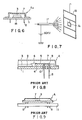
- In the drawings:
- FIG. 1 is a partial sectional side view of a first preferred embodiment of the present invention illustrating the essential details of construction;
- FIG. 2 is a sectional side view illustrating the construction of the entire device of the first preferred embodiment;
- FIG. 3 is a plan view showing a glass-epoxy
- FIGS. 4, 5 and 6 are sectional side views illustrating second, third and fourth preferred embodiments, respectively, of the present invention;
- FIG. 7 is a schematic perspective view indicating an electrostatic particle spraying process;
- FIG. 8 is a partial sectional side view illustrating the essential details of a conventional semiconductor device; and
- FIG. 9 is a sectional side view of the same device mounted on a printed circuit board.
- Referring now to FIGS. 1 to 3, a first embodiment of the present invention will be described. A
semiconductor chip 3 is mounted over an interposedsilver paste 2 at substantially the center portion of a rectangular metal package base 1. The electrodes of thesemiconductor chip 3 are connected throughbonding wires 6 to theircorresponding wires 5 printed over the surface of a printed-wire board 4 disposed so as to surround thesemiconductor chip 3. The space above thesemiconductor chip 3 and theboard 4 is covered and hermetically sealed by ametal cover plate 7.Lead pins 8 are extended through the package base 1 and downwardly beyond the bottom surface thereof and their upper ends are connected to theircorresponding wires 5 withsolder 9. The annular space between eachlead pin 8 and the inner wall surface of each lead-pin hole is sealed with a sealingmaterial 10 such as glass. Attached to the bottom surface of the package base 1 with an epoxy resin adhesive is abase plate 13 comprising a glass screen which is an electrically insulator member and is impregnated with an epoxy resin. - The epoxy-impregnated
glass screen board 13 is formed with a plurality of throughholes 13a at respective positions corresponding to thelead pins 8 as shown in FIG. - 3.
- Instead of the epoxy-impregnated
glass base plate 13 which is an insulator, a crepe paper mica, a silicone rubber or the like may be used. Furthermore, as an adhesive 14, in addition to the above-described epoxy resin adhesive, a novolak adhesive, a siliconeadhesive, a varnish adhesive and so on may be used. - Furthermore, an
insulating coating 15 comprising electrically insulating particles or liquid is applied over the entire surface of themetal cover plate 7. Thus, the semiconductor device A₁ is obtained. - The above mentioned coating particles are, for instance, those of an epoxy resin, and the liquid coating material is, for instance, one of varnish-epoxy series.
- In the case of spraying the
insulating coating 15, for instance, as shown in FIG. 7, a so-called electrostatic coating is used. That is, the semiconductor device A₁ is suspended from ametal frame 16 which is a cathode and is grounded and a coating material such as an epoxy resin is used as an anode. A voltage of the order of 60 KV is applied to aspray gun 17 so as to spray the coating material over the entire surface of themetal cover plate 7, thereby coating the latter with the insulating material. - The electrically insulating epoxy-impregnated
glass base plate 13 is attached to the bottom surface of the package base 1 so that the package base 1 and the printed circuit board 11 upon which the semiconductor device A₁ is mounted can be electrically isolated from each other (FIG. 10) so that the path (1) extending from the printed-circuit board 11 to the bottom surface of thesemiconductor chip 3 can be completely cut off. Since the entire surface of themetal cover plate 7 is coated with an electrically insulating coating material, even if themetal cover plate 7 should contact a peripheral wire, they are completely electrically isolated from each other. As a result, the path (2) extending from the peripheral wire in contact with themetal cover plate 7 to the bottom surface of thesemiconductor chip 3 can be also completely closed. - In a second embodiment of the present invention shown in FIG. 4, the coating of the entire surface of the
metal cover plate 7 with the electrically insulatingcoating material 15 is eliminated in the case of the fabrication of a semiconductor device A₂ so that the package base 1 and the printed-circuit board 11 (FIG> 10) can be completely electrically isolated from each other. - In a third embodiment of the present invention shown in FIG. 5, the electrically insulating
coating material 15 is sprayed by the electrostatic coating process over the bottom surface of the package base 1 and the entire surface of themetal cover plate 7 in the case of the fabrication of a semiconductor device A₃. - In a fourth embodiment of the present invention shown in FIG. 6, the bottom surface of the package base 1 and the entire surface of the
metal cover plate 7 are not coated with an electrically insulating coating material, but thesemiconductor chip 3 is mounted over all intervening electrically insulatingadhesive 18 on the upper surface of the package base 1 in the case of the fabrication of a semiconductor device A₄. Therefore the package base 1 and thesemiconductor chip 3 are completely electrically isolated from each other so that the bottom surface of thesemiconductor chip 3 and the package base 1 are prevented from being at the same potential. - The
insulating adhesive 18 is, for instance, an epoxy resin. In the case of this epoxy-series resin, it is preferable to admix therewith a filler (SiO₂ or the like) in excess of about 30 microns in order to maintain stable electrical isolation. In this case, the insulation resistance between the semiconductor device A₄ and the package base 1 can be maintained at less than 10 MΩ until the applied voltage reaches 100 V.
Claims (3)
a metal package base;
a semiconductor chip mounted on the upper surface of said package base;
a metal cover plate covering and air-tightly sealing and
an insulator attached to the bottom surface of said package base.
a metal package base;
semiconductor chip mounted on the upper surface of said package base;
a metal cover plate covering and air-tightly sealing; and
an electrically insulating compound coating the bottom surface of said package base and the entire outer surface of said metal cover plate.
a metal package base;
a semiconductor chip mounted over an interposed electrically insulating adhesive on the upper surface of said package base; and
a metal cover plate covering and air-tightly sealing.
Applications Claiming Priority (2)
| Application Number | Priority Date | Filing Date | Title |
|---|---|---|---|
| JP39034/88 | 1988-02-22 | ||
| JP63039034A JPH0783070B2 (en) | 1988-02-22 | 1988-02-22 | Semiconductor device |
Publications (2)
| Publication Number | Publication Date |
|---|---|
| EP0338213A2 true EP0338213A2 (en) | 1989-10-25 |
| EP0338213A3 EP0338213A3 (en) | 1990-11-07 |
Family
ID=12541829
Family Applications (1)
| Application Number | Title | Priority Date | Filing Date |
|---|---|---|---|
| EP19890103083 Withdrawn EP0338213A3 (en) | 1988-02-22 | 1989-02-22 | Semiconductor device with a metal package |
Country Status (3)
| Country | Link |
|---|---|
| EP (1) | EP0338213A3 (en) |
| JP (1) | JPH0783070B2 (en) |
| KR (1) | KR920003436B1 (en) |
Cited By (5)
| Publication number | Priority date | Publication date | Assignee | Title |
|---|---|---|---|---|
| US5098864A (en) * | 1989-11-29 | 1992-03-24 | Olin Corporation | Process for manufacturing a metal pin grid array package |
| US5103292A (en) * | 1989-11-29 | 1992-04-07 | Olin Corporation | Metal pin grid array package |
| EP0544538A2 (en) * | 1991-11-27 | 1993-06-02 | Shinko Electric Industries Co. Ltd. | Coaxial line assembly |
| WO1996035233A1 (en) * | 1995-05-05 | 1996-11-07 | Blaupunkt-Werke Gmbh | Cover for an electronic component |
| WO2014133838A1 (en) * | 2013-02-28 | 2014-09-04 | Cooper Technologies Company | External moisture barrier package for circuit board electrical component |
Families Citing this family (3)
| Publication number | Priority date | Publication date | Assignee | Title |
|---|---|---|---|---|
| JPH079953B2 (en) * | 1988-04-13 | 1995-02-01 | 株式会社東芝 | Method for manufacturing semiconductor device |
| US6262477B1 (en) * | 1993-03-19 | 2001-07-17 | Advanced Interconnect Technologies | Ball grid array electronic package |
| JP2797995B2 (en) * | 1995-03-16 | 1998-09-17 | 日本電気株式会社 | Semiconductor device |
Citations (2)
| Publication number | Priority date | Publication date | Assignee | Title |
|---|---|---|---|---|
| EP0084866A2 (en) * | 1982-01-21 | 1983-08-03 | Olin Corporation | Semiconductor casing |
| EP0122687A2 (en) * | 1983-03-18 | 1984-10-24 | Mitsubishi Denki Kabushiki Kaisha | A semiconductor device comprising packing means for protecting parts of the device |
Family Cites Families (3)
| Publication number | Priority date | Publication date | Assignee | Title |
|---|---|---|---|---|
| JPS5227374A (en) * | 1975-08-27 | 1977-03-01 | Hitachi Ltd | Semiconductor device |
| JPS6175548A (en) * | 1984-09-21 | 1986-04-17 | Hitachi Ltd | Semiconductor device |
| JPS6323341A (en) * | 1987-07-14 | 1988-01-30 | Toshiba Corp | Solid state device and manufacture thereof |
-
1988
- 1988-02-22 JP JP63039034A patent/JPH0783070B2/en not_active Expired - Fee Related
-
1989
- 1989-02-22 EP EP19890103083 patent/EP0338213A3/en not_active Withdrawn
- 1989-02-22 KR KR1019890002090A patent/KR920003436B1/en not_active IP Right Cessation
Patent Citations (2)
| Publication number | Priority date | Publication date | Assignee | Title |
|---|---|---|---|---|
| EP0084866A2 (en) * | 1982-01-21 | 1983-08-03 | Olin Corporation | Semiconductor casing |
| EP0122687A2 (en) * | 1983-03-18 | 1984-10-24 | Mitsubishi Denki Kabushiki Kaisha | A semiconductor device comprising packing means for protecting parts of the device |
Non-Patent Citations (5)
| Title |
|---|
| IBM TECHNICAL DISCLOSURE BULLETIN. vol. 18, no. 3, August 1975, NEW YORK US pages 751 - 752; J.M.AMARO ET AL.: "Back sealing electronic modules" * |
| IBM TECHNICAL DISCLOSURE BULLETIN. vol. 30, no. 2, July 1987, NEW YORK US page 546 "Plastic/metal hybrid package" * |
| PATENT ABSTRACTS OF JAPAN vol. 10, no. 386 (E-467)(2443) 24 December 1986, & JP-A-61 177760 (HITACHI MICRO COMPUT ENG LTD) 09 August 1986, * |
| PATENT ABSTRACTS OF JAPAN vol. 11, no. 325 (E-551)(2772) 22 October 1987, & JP-A-62 114244 (MATSUSHITA ELECTRIC WORKS LTD) 26 May 1987, * |
| PATENT ABSTRACTS OF JAPAN vol. 12, no. 146 (E-605)(2993) 06 May 1988, & JP-A-62 263660 (NISSIN ELECTRIC CO) 16 November 1987, * |
Cited By (7)
| Publication number | Priority date | Publication date | Assignee | Title |
|---|---|---|---|---|
| US5098864A (en) * | 1989-11-29 | 1992-03-24 | Olin Corporation | Process for manufacturing a metal pin grid array package |
| US5103292A (en) * | 1989-11-29 | 1992-04-07 | Olin Corporation | Metal pin grid array package |
| EP0544538A2 (en) * | 1991-11-27 | 1993-06-02 | Shinko Electric Industries Co. Ltd. | Coaxial line assembly |
| EP0544538A3 (en) * | 1991-11-27 | 1993-08-11 | Shinko Electric Industries Co. Ltd. | Coaxial line assembly |
| US5557074A (en) * | 1991-11-27 | 1996-09-17 | Fujitsu Limited | Coaxial line assembly of a package for a high frequency element |
| WO1996035233A1 (en) * | 1995-05-05 | 1996-11-07 | Blaupunkt-Werke Gmbh | Cover for an electronic component |
| WO2014133838A1 (en) * | 2013-02-28 | 2014-09-04 | Cooper Technologies Company | External moisture barrier package for circuit board electrical component |
Also Published As
| Publication number | Publication date |
|---|---|
| KR920003436B1 (en) | 1992-05-01 |
| JPH01214052A (en) | 1989-08-28 |
| KR890013753A (en) | 1989-09-25 |
| JPH0783070B2 (en) | 1995-09-06 |
| EP0338213A3 (en) | 1990-11-07 |
Similar Documents
| Publication | Publication Date | Title |
|---|---|---|
| US5309021A (en) | Semiconductor device having particular power distribution interconnection arrangement | |
| US3280378A (en) | Means for anchoring and connecting lead wires in an electrical component | |
| US4677520A (en) | Static charge protector for integrated circuits | |
| EP0806835A3 (en) | Electronic component | |
| EP0338213A2 (en) | Semiconductor device with a metal package | |
| KR900007301B1 (en) | Semiconductor package | |
| US4992851A (en) | Characteristic impedance-correct chip carrier for microwave semiconductor components | |
| US4400645A (en) | CRT Socket assembly | |
| US6437430B2 (en) | Semiconductor apparatus and frame used for fabricating the same | |
| US3956672A (en) | In line rectifier assembly | |
| US5331334A (en) | Vacuum fluorescent display device | |
| JPH1140709A (en) | Semiconductor mounting structure and manufacture thereof | |
| JPH05259373A (en) | Power semiconductor device | |
| JP3375283B2 (en) | Semiconductor device and circuit module including the same | |
| JPH0766313A (en) | Composite electronic parts | |
| JPH08316656A (en) | Package for electronic component | |
| JPS60235443A (en) | Semiconductor device | |
| JPH0526800Y2 (en) | ||
| KR19990088201A (en) | Fluorescent display device | |
| KR20000071262A (en) | Electrical device | |
| JPS61252652A (en) | Resin sealed type semiconductor device | |
| JP2000023352A (en) | Protector for communication equipment | |
| JPH0727614Y2 (en) | High voltage variable resistor block | |
| JPS6084842A (en) | Semiconductor ic package | |
| GB895568A (en) | Improvements in or relating to capacitors |
Legal Events
| Date | Code | Title | Description |
|---|---|---|---|
| PUAI | Public reference made under article 153(3) epc to a published international application that has entered the european phase |
Free format text: ORIGINAL CODE: 0009012 |
|
| 17P | Request for examination filed |
Effective date: 19890222 |
|
| AK | Designated contracting states |
Kind code of ref document: A2 Designated state(s): DE FR GB IT |
|
| RAP1 | Party data changed (applicant data changed or rights of an application transferred) |
Owner name: KABUSHIKI KAISHA TOSHIBA Owner name: TOSHIBA MICRO-ELECTRONICS CORPORATION |
|
| PUAL | Search report despatched |
Free format text: ORIGINAL CODE: 0009013 |
|
| RHK1 | Main classification (correction) |
Ipc: H01L 23/14 |
|
| AK | Designated contracting states |
Kind code of ref document: A3 Designated state(s): DE FR GB IT |
|
| 17Q | First examination report despatched |
Effective date: 19920930 |
|
| STAA | Information on the status of an ep patent application or granted ep patent |
Free format text: STATUS: THE APPLICATION IS DEEMED TO BE WITHDRAWN |
|
| 18D | Application deemed to be withdrawn |
Effective date: 19931130 |