EP0338781A2 - Data transmission and recording - Google Patents
Data transmission and recording Download PDFInfo
- Publication number
- EP0338781A2 EP0338781A2 EP89303837A EP89303837A EP0338781A2 EP 0338781 A2 EP0338781 A2 EP 0338781A2 EP 89303837 A EP89303837 A EP 89303837A EP 89303837 A EP89303837 A EP 89303837A EP 0338781 A2 EP0338781 A2 EP 0338781A2
- Authority
- EP
- European Patent Office
- Prior art keywords
- data
- bits
- mode
- unit
- bit
- Prior art date
- Legal status (The legal status is an assumption and is not a legal conclusion. Google has not performed a legal analysis and makes no representation as to the accuracy of the status listed.)
- Granted
Links
Images


Classifications
-
- G—PHYSICS
- G11—INFORMATION STORAGE
- G11B—INFORMATION STORAGE BASED ON RELATIVE MOVEMENT BETWEEN RECORD CARRIER AND TRANSDUCER
- G11B20/00—Signal processing not specific to the method of recording or reproducing; Circuits therefor
- G11B20/10—Digital recording or reproducing
- G11B20/18—Error detection or correction; Testing, e.g. of drop-outs
- G11B20/1806—Pulse code modulation systems for audio signals
- G11B20/1809—Pulse code modulation systems for audio signals by interleaving
-
- G—PHYSICS
- G11—INFORMATION STORAGE
- G11B—INFORMATION STORAGE BASED ON RELATIVE MOVEMENT BETWEEN RECORD CARRIER AND TRANSDUCER
- G11B20/00—Signal processing not specific to the method of recording or reproducing; Circuits therefor
- G11B20/10—Digital recording or reproducing
- G11B20/10527—Audio or video recording; Data buffering arrangements
-
- G—PHYSICS
- G11—INFORMATION STORAGE
- G11B—INFORMATION STORAGE BASED ON RELATIVE MOVEMENT BETWEEN RECORD CARRIER AND TRANSDUCER
- G11B20/00—Signal processing not specific to the method of recording or reproducing; Circuits therefor
- G11B20/10—Digital recording or reproducing
- G11B20/12—Formatting, e.g. arrangement of data block or words on the record carriers
- G11B20/1201—Formatting, e.g. arrangement of data block or words on the record carriers on tapes
- G11B20/1207—Formatting, e.g. arrangement of data block or words on the record carriers on tapes with transverse tracks only
- G11B20/1208—Formatting, e.g. arrangement of data block or words on the record carriers on tapes with transverse tracks only for continuous data, e.g. digitised analog information signals, pulse code modulated [PCM] data
-
- H—ELECTRICITY
- H04—ELECTRIC COMMUNICATION TECHNIQUE
- H04N—PICTORIAL COMMUNICATION, e.g. TELEVISION
- H04N5/00—Details of television systems
- H04N5/76—Television signal recording
- H04N5/91—Television signal processing therefor
- H04N5/92—Transformation of the television signal for recording, e.g. modulation, frequency changing; Inverse transformation for playback
- H04N5/928—Transformation of the television signal for recording, e.g. modulation, frequency changing; Inverse transformation for playback the sound signal being pulse code modulated and recorded in time division multiplex with the modulated video signal
-
- H—ELECTRICITY
- H04—ELECTRIC COMMUNICATION TECHNIQUE
- H04N—PICTORIAL COMMUNICATION, e.g. TELEVISION
- H04N9/00—Details of colour television systems
- H04N9/79—Processing of colour television signals in connection with recording
- H04N9/7921—Processing of colour television signals in connection with recording for more than one processing mode
- H04N9/7925—Processing of colour television signals in connection with recording for more than one processing mode for more than one standard
-
- G—PHYSICS
- G11—INFORMATION STORAGE
- G11B—INFORMATION STORAGE BASED ON RELATIVE MOVEMENT BETWEEN RECORD CARRIER AND TRANSDUCER
- G11B20/00—Signal processing not specific to the method of recording or reproducing; Circuits therefor
- G11B20/10—Digital recording or reproducing
- G11B20/10527—Audio or video recording; Data buffering arrangements
- G11B2020/10537—Audio or video recording
- G11B2020/10546—Audio or video recording specifically adapted for audio data
-
- G—PHYSICS
- G11—INFORMATION STORAGE
- G11B—INFORMATION STORAGE BASED ON RELATIVE MOVEMENT BETWEEN RECORD CARRIER AND TRANSDUCER
- G11B20/00—Signal processing not specific to the method of recording or reproducing; Circuits therefor
- G11B20/10—Digital recording or reproducing
- G11B2020/1087—Digital recording or reproducing wherein a selection is made among at least two alternative ways of processing
-
- G—PHYSICS
- G11—INFORMATION STORAGE
- G11B—INFORMATION STORAGE BASED ON RELATIVE MOVEMENT BETWEEN RECORD CARRIER AND TRANSDUCER
- G11B2220/00—Record carriers by type
- G11B2220/90—Tape-like record carriers
Definitions
- This invention relates to data transmission and recording, and more particularly to data transmission apparatus capable of operating in either of two modes, to apparatus for receiving data so transmitted, and to apparatus for recording pulse code modulated (PCM) audio signals.
- PCM pulse code modulated
- an audio signal is recorded by mixing it with a colour video signal such that the audio signal is separated in terms of frequency from the colour signal when both are subjected to frequency modulation, or as an alternative, the audio signal can be subjected to PCM and separated, in terms of recording location, from the colour signal, and in both cases the recording can be made with each track comprising both signals.
- VTR video tape recorder
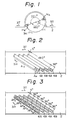
- Figure 1 shows one example of a rotary head device of an 8-mm VTR, and figure 2 shows its tape format.
- rotary magnetic heads HA and HB for recording and reproducing have different azimuth angles, are angularly spaced at 180°, and are rotated in the direction 3H at a frequency (30 Hz) on a drum 1 from the circumference of which they project slightly.
- a magnetic tape 2 is wrapped around the drum 1 over an angular range of 221°, and runs at a constant speed in the direction 3T.
- Oblique tracks 4A and 4B having a length corresponding to 221° are therefore formed alternately on the tape 2 by the heads HA and HB as shown in Figure 2, and a signal is recorded.
- an area AP of the tracks 4A and 4B corresponding to an angular range of about 36° from the time when the heads HA and HB start scanning, and containing a margin for after-recording and a guard band for distinguishing between the area AP and an area AV
- an audio signal associated with one field of a video signal is recorded in a PCM time-compressed state.
- a colour video signal of one field, a frequency modulated (FM) audio signal and a signal for tracking are recorded.
- FIG. 3 shows a track format for recording a PCM audio signal on areas AP2 to AP6 respectively which are formed by dividing the area AV ( Figure 2) into angular ranges of 36°, thereby enabling recording of six audio channels in the areas AP1 to AP6.
- the PCM audio signal in the above-mentioned 8-mm VTR has 8-bit words and is slightly inferior in terms of performance as compared with a compact disc (CD) or a digital audio tape.
- audio data having 12-bit words can be recorded at a sampling frequency of 48 kHz on metal power tape (MP tape) comprising metal power and a binder, and audio data having 16-bit words can be recorded at the sampling frequency of 48 kHz on metal evaporated tape (ME tape).
- MP tape metal power tape
- ME tape metal evaporated tape
- the number of bits per word of the audio data can be increased.
- MP mode 12-bit audio data
- ME mode 16-bit audio data
- a previously proposed digital audio tape recorder is constructed so that it can assume a 16-bit mode and a 12-bit mode.
- the sampling frequency fs is 48 kHz in the 16-bit mode, and 32 kHz in the 12-bit mode, in which the speed of the magnetic tape and the speed of the rotary head drum are reduced to half to permit longer recording.
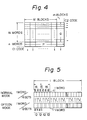
- Figure 4 shows a code structure of a PCM audio signal and redundant data of the error correction code which are recorded on one segment formed by one scan of a rotary head.
- each vertical column of the two-dimensional array comprises one block, and M blocks are arranged in the horizontal direction.
- a PCM audio signal in one block is composed of N words.
- An error detection code C1 is added to each block in the vertical direction of the array, and an error correction code C2 is added in the horizontal direction.
- An n-word check mode P of the error detection code C1 is contained in each column, and the error detection code C1 also relates to an m-word check code Q of the error correction code C2.
- the sizes of the two-dimensional arrays over which the encoding of C1 and C2 is done are the same for the 12-bit mode and the 16-bit mode.
- the length of one block data which is one code sequence of the code C1 is selected to be the least common multiple L of 16 and 12, multiplied by an integer, and the number of bits per block is made the same in both modes.
- the 16-bit words comprise an upper (that is, more significant) eight-bit symbol and a lower (that is, less significant) eight-bit symbol to form an error correction code
- the 12-bit words as shown in Figure 5, exactly the same error correction encoding process as the case of the 16-bit words is performed after allotting its upper eight bits and lower four bits.
- the sampling frequency of the audio signal, the transport speed of the magnetic tape and the rotational speed of the rotary heads are not changed with the 12-bit and 16-bit modes.
- the recording is made in the PCM audio area AP with an adequate recording wavelength per bit depending on the tape type (ME/MP), and the transmission bit rate is not the same in both modes as it is in a DAT.
- the sizes of the two-dimensional arrays of the PCM audio signal are different in the two modes.
- Figures 6A and 6B show respective examples of a two-dimensional array of error correction blocks of a one-word-16-bit mode and a one-word-12-bit mode for NTSC.
- the arrays are stored in a memory.
- a header comprising the block synchronization signal and block address data is indicated in the case where the header is added to each block.
- one sequence of the error correction code C2 in the horizontal direction is composed of symbols which occur every four bytes. Consequently one row in the horizontal direction has four sequences for the error correction code C2.
- one sequence of the code C2 is formed by a (25, 20, 6) Reed-Solomon code having a five-byte check code per sequence.
- a check code Q of a total of 20 bytes for four sequences is added to the left of each row of the PCM audio data as shown in Figure 6A.
- one sequence of the error correction code C2 is composed of symbols which lie every three bytes to make one row in the horizontal direction.
- One sequence of the code C2 is formed by a (25, 20, 6) Reed-Solomon code in a manner similar to the 16-bit mode, and a five-byte check code Q is developed per one sequence.
- a check code of a total of 15 bytes is added to the left of the audio PCM data as indicated in Figure 6B.
- the 4-byte data can be dealt with adequately by inserting it into the header.
- the technique described in the above-mentioned US patent application 252,807 can be employed for inserting four symbols in the header.
- the error correction code C1 in the vertical direction is the same for both modes, and a (44, 40, 5) Reed-Solomon code, for example, is used.
- data transmission apparatus capable of selecting a first mode in which one data unit is made up of m bits and a second mode is which one data unit is made up of n bits (m > n) with the same sampling frequency
- the apparatus comprising: error-correction encoding means commonly used for the first and second modes; insertion means for inserting (m - n) insertion bits of dummy data into said data unit; elimination means for eliminating said (m - n) insertion bits from the data unit; and addition means for adding header information including at least a block synchronization signal to the data; in said first mode, m-bit data units are subjected to an encoding process at said error-correction encoding means, a block synchronization signal for one-unit-m-bits data is added for every block of the encoded data at said addition means, and data from the addition means is transmitted; and in said second mode, said insertion bits are inserted in each data unit of one-unit-n-bits data, at said insertion
- apparatus for receiving data selectively transmitted in a first mode in which one unit is made up of m bits or in second mode in which one unit is made up of n bits (m > n) with the same sampling frequency
- the apparatus comprising: switching signal generating means for detecting whether the received data are first mode data or second mode data and generating a mode switching signal in dependence thereon; insertion means for inserting (m - n) insertion bits of dummy data; error-correction decoding means used commonly for the first and modes; and elimination means for eliminating the (m - n) insertion bits from the data; when the first mode is selected by said mode switching signal, the received data are subjected to an error-correction decoding process at said error-correction decoding means, and one-unit-m-bit data are decoded; and when the second mode is selected by said mode switching signal, the received data are supplied to said insertion means so that said insertion bits are inserted in every unit of the one-unit-n-bit data to
- apparatus for recording a PCM audio signal on a magnetic tape medium by magnetic heads, and capable of selecting a first mode in which one unit is made up of m bits and a second mode in which one unit is made up of n bits (m > n) with the same sampling frequency
- the apparatus comprising: error-correction encoding means used commonly for the first and second modes; insertion means for inserting (m - n) insertion bits of dummy data into said unit data; elimination means for eliminating said (m - n) insertion bits from the data; and addition means for adding header information including at least a block synchronization signal to the data; in said first mode, data whose units are of m bits are subjected to an encoding process at said error-correction encoding means, a block synchronization signal for one-unit-m-bit data is added for every block of the encoding-processed data at said addition means, and data from the addition means are transmitted; and in said second mode, said insertion bits
- a data transmission apparatus capable of selecting a first mode in which one data word is made up of m bits with a predetermined sampling frequency and a second mode in which one data word is composed of n bits (m > n) with the same sampling frequency, comprises error correction encoding means commonly used for the first and second modes, insertion means for inserting bits (dummy data) of (m - n) bits into the data words of n bits, means for eliminating the inserted (m - n) bits from the data, and means for adding a block synchronization signal to the data.
- a data reception apparatus for receiving transmission data from said data transmission apparatus, comprises synchronization detection means for detecting the block synchronization signal from the transmission data, switching siganl generating means for deciding whether the detected block synchronization signal is a first block synchronization signal or a second block synchronization and generating a mode switching signal, insertion means for inserting bits (dummy data) of (m - n) bits, error correction decoding means used commonly for the first and second modes, and elimination means for eliminating the inserted bits (dummy data) of (m - n) bits from data.
- the switching signal generating means can comprise means for generating a mode switching signal by decoding an identification code when an identification code for the first mode and the second mode has been added to the data.
- a block synchronization signal for one-word-m-bits is added for every block of the encoding-processed data at said addition means and data from the addition means is transmitted.
- said inserted bits (dummy data) are inserted for one word of one-word-n-bit data at said insertion means so as to make one-word-m-bit data, these data are supplied to said error correction encoding means, subjected to an encoding process, said inserted bits (dummy data) are eliminated from the encoding-processed data at said elimination circuit to form one-word-n-bit data, data from the eliminating circuit is supplied to said addition means, a block synchronization signal for one-word-n-bits is added for every block, and data from the addition means is transmitted.
- the data from said synchronization detection means is subjected to an error-correction decoding process at said error-correction decoding means, and one-word-m-bit data are decoded
- the data from said synchronization detection means are supplied to said insertion means so that said inserted bits (dummy data) are inserted for every word of the one-word-n-bit data to make one-word-m-bit data, these data are supplied to said error-correction decoding means and decoding processed, and decoding-processed data is fed to said elimination means and said inserted bits (dummy data) are eliminated so as to decode the one-word-n-bit data.
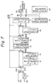
- Figure 7 shows an embodiment of data transmission apparatus in which the invention is applied to a recording system for PCM audio data in an 8-mm VTR.
- the apparatus comprises mode switching circuits MS1 to MS5, each of which is switched to engage a terminal A by a mode switching signal MDR from a terminal 6 in a one-word-16-bits mode (hereinafter called the "A mode” or “ME mode”), and to engage a terminal B by the mode switching signal MDR in a one-word-12-bits mode (hereinafter called the "B mode” or “MP mode”).
- the mode switching signal MDR results, for example, from a user operating a switch, and/or a metal powder tape and a metal evaporated tape can be distinguished automatically by an identification means such as a hole in the cassette, and the mode switching signal MDR is then automatically supplied in response to the output of the identification means.
- SW1 is a switch circuit for switching manually or automatically between digital and analogue input audio data.
- Digital audio data derived from a CD, DAT or the like is supplied to a terminal DT of the switch circuit SW1 through an input terminal 5D.
- the digital audio data is two-channel data for right and left channels and is parallel data, consisting of 16-bit words with a sampling frequency of 48 kHz.
- An analogue audio signal derived from an FM tuner, television receiver, microphone or the like (left and right channels) is supplied to an analogue-to-digital (A/D) converter 11 through an input terminal 5A, sampled at the sampling frequency of 48 kHz, converted to 16-bit word parallel data, and supplied to a terminal AD of the switch circuit SW1.
- A/D analogue-to-digital
- the A mode will be described first.
- 16-bit word data from the switch circuit SW1 is supplied to a word/symbol converter 14 through the switch circuits MS1 and MS2, and is converted into a symbol comprising upper and lower eight bits.
- the symbol data is supplied to an error correction encoder 15 and subjected to an error-correction encoding process on a Galois field GF 28.
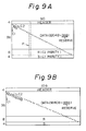
- Figures 9A and 9B show a two-dimensional array of audio data of one field to be recorded in a PCM audio area AP in the A mode.
- Figure 9A is suitable for the NTSC system
- Figure 9B is suitable for the CCIR system.
- each column in the longitudinal direction comprises one block, 90 blocks are arranged in the horizontal direction for NTSC, and 109 blocks are arranged in the horizontal direction for CCIR.
- One block contains a 36-symbol PCM audio signal, so the arrays shown accept 3240 symbols (byte) (3204 bytes of data and 36 bytes reserve) of PCM audio signals for NTSC, or 3888 symbols (3840 bytes of data and 48 bytes reserve) of PCM audio signals for CCIR.
- An error correction code C2 for instance, a (44, 46, 9) Reed-Solomon code is formed in the diagonal direction of the arrays and an 8-symbol check code R is derived and added to the lower side of the PCM audio signals.
- the error correction code C2 in the diagonal direction sequentially contains symbols at positions shifted by two symbols in the horizontal direction when shifted by one symbol in the longitudinal direction, in the NTSC system, and at positions shifted by three, two, three, two, two, this sequence repeating in the horizontal direction, when shifted by one in the longitudinal direction, in the CCIR system.
- an 8-symbol check code R of the error correction code C2 is added to the array, and an error detection or correction code C1, for example, a (48, 44, 5) Reed-Solomon code is derived to add a 4-symbol check code S in the longitudinal direction.
- a 4-byte header comprising a 1-byte block synchronization signal and three bytes including a block address signal is added at the start position of each block in the longitudinal direction, and one block, for example block P having a structure as shown in Figure 12A, containing header information, is added by an adder 18 as mentioned later, and is not added in the encoding process.
- the header may be added in the encoding process and the information of the header may then be error-encoding-processed as data.
- the error correction code C2 may be in the form of two sequences of symbols alternating in the longitudinal direction, with a (22, 18, 5) Reed-Solomon code, for example, applied to the respective sequences. In this way the load on an error correcting encoder 15 can be reduced.
- odd number data Llu, Lll, L3u, L3l, ..., Rlu, Rll, R3u, R3l, ... of the left and right channel audio data are separately arranged in the left and right sides of the array as shown, in which suffixes u and l indicate the upper 8-bit symbol and the lower 8-bit symbol of the 16-bit word respectively.
- the even number data and the odd number data are recorded at separate positions, with the data sequentially recorded in the longitudinal direction, so that even if either the even number data or the odd number data is lost due to a burst error, error correction can easily be effected by average interpolation using the remaining data.
- the output of the error correction encoder 15 is fed to a 8-10 modulator 17 through the switch circuits MS3 and MS4, and 8-bit symbol data are converted into 10-bit data.
- the output of the 8-10 modulator 17 is supplied to the adder 18.
- the 8-10 modulator 17 is provided for preventing errors caused by a dc component in a recording data, and generates 10-bit data with a reduced dc component.
- a 16-bit block synchronization signal SYNC and an address signal are supplied to the adder 18 through the switch circuit MS5 from a header signal generator 19 and are added to the data. Also, an identification signal ID for distinguishing the A mode from the B mode may be inserted in the header signal and added to the data.
- the output of the adder 18 is supplied to a parallel-serial converter 20 where it converted into serial data sequentially from the left of the array of Figure 9, and the serial data are supplied to rotary magnetic heads for recording on a magnetic tape.
- 16-bit word data from the switch circuit MS1 is supplied to a 16 to 12 compression circuit 12 which for example, performs non-linear compression for form 12-bit word data which is supplied to an insertion circuit 13.
- the 4-bit dummy data, that is 0000 is added to the 12-bit data to form 16-bit data.
- each upper symbol is made up of the upper four bits of the 12-bit word and the four insertion bits.
- the 16-bit data from the insertion circuit 13 is supplied to a word/symbol converter 14 through the switch circuit MS2, where they are converted into symbol data, and are then supplied to the error correction encoder 15 so that the error correction codes C1 and C2 can be added in a similar manner to the A mode.
- the data contained in one block corresponds to 27 bytes in the B mode, that is counting only data and excluding the insertion bits (dummy data).
- 27 bytes in the longitudinal direction does not include the dummy data, and after inserting the dummy data, the array having 36 bytes in the longitudinal direction is formed in a memory of an error correction encoder 15.
- the two-dimensional data array contains 2430 bytes (2403 bytes of data and 27 bytes reserve) in NTSC as shown in Figure 10A, and 2916 bytes (2880 bytes of data and 36 bytes reserve) in CCIR as shown in Figure 10B.
- the reserve bytes are provided to identify the character of the PCM audio signal.
- Data from the error correction encoder 15 are supplied to an insertion-data eliminating circuit 16 through the switch MS3 for the elimination of the four insertion bits.
- block data comprising 12-bit words (27-byte data and parities R, S) are obtained as shown in Figure 12C, which are supplied to the 8-10 modulator 17 through the switch circuit MS4, converted into 10-bit data, and then supplied to the adder 18.
- a 12-bit block synchronization signal, etc. are produced by a header signal generator 21 for each block, and are supplied to the adder 18 through the switch circuit MS5 and added to the data.
- the output signal of the adder 18 is recorded together with a video signal after being passed through the parallel-serial converter 20.
- the four insertion bits are added on the side of the upper bits of a 12-bit word, but as an alternative they can be added on the side of the lower bits of the 12-bit word.
- the insertion bits may be added so that they are added on the lower-bit side of odd number words and on the upper-bit side of even number words (that is, words having odd and even addresses respectively in the block.
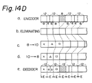
- Figure 14A-a shows the case of inserting the dummy data (the hatched portion) only at the upper-bit side of each word.
- the output data of the eliminating circuit 16 become only the true 8-bit data as shown in Figure 14A-b.
- This 8-bit data is converted to 10-bit data by the 8-10 modulator 17, and the output data of the 8-10 modulator 17 are recorded/reproduced magnetically ( Figure 14A-c).
- Figure 14A-c Consider a case in which a one-byte error appears in the output of the 10-8 demodulator 27 (shown by mark X, ⁇ or ⁇ in Figure 14A-d) having occurred in the process of magnetic recording/reproducing.
- the one-byte-errors shown by marks X and ⁇ in Figure 14A-e are spread between two bytes at the error correction decoder 29 after insertion of the dummy data.
- the cycle of the error correcting operation of the encoder 29 is indicated by E in the drawings so that, the error bits marked X, for example, are spread between two operational cycles.
- Figure 14B shows the case of inserting the dummy data (the hatched portion) only at the lower-bit side of each word (the lower side of the lower symbol), and a detailed description thereof will be omitted herein for the sake of brevity.
- one-byte errors shown by marks ⁇ and ⁇ in Figure 14B become two-byte-errors respectively at the error correction decoder 29 similarly to Figure 14A.
- Figure 14C shows the case of inserting two dummy data of four bits to the upper-bit side and the lower-bit side, respectively of alternate words respectively. In this case, only a one-byte-error shown by mark ⁇ in Figure 14C becomes a two-byte-error at the error correction decoder 29.
- Figure 14D shows the case of inserting dummy data having eight bits.
- one-byte-errors shown by marks X, ⁇ and ⁇ in Figure 14D do not cause two-byte errors, thereby eliminating degradation of the error correction.
- a common generating circuit for the header signal may be employed for both modes, and the header-signal-generation period is varied depending on the block period in the A mode and the B mode respectively, by controlling the generating circuit with a mode switching signal.
- Figure 8 shows an embodiment of reproduction apparatus comprising mode switching circuits MS6 to MS9, each of which engages a terminal A for the A mode and engages a terminal B for the B mode under the control of a mode switching signal MDP which will be described below.
- PCM audio data derived from a signal from a rotary reproducing head is supplied to a block synchronization signal detector 23 through an input terminal 22.
- the PCM audio data supplied through the input terminal 22 is supplied to a phase locked loop (PLL) circuit 24, and as a result a clock signal synchronized with the reproduced signal is derived.
- the clock signal is supplied to the detector 23 and the block synchronization signal is detected.
- the detected block synchronization signal is supplied to a switching signal generator 25, and by detecting the detected period it is determined whether the reproduced signal is of the A mode or the B mode, and the mode switching signal MDP is developed accordingly.
- data in which the block synchronization signal has been detected is serial-to-parallel converted by a serial-parallel converter 26 and supplied to a 10-8 demodulator 27 where 10-bit data are converted into 8-bit symbol data.
- the symbol data are supplied to an error correction decoder 29 through switch circuits MS6 and MS7 and subjected to error correction processing using the error detection or correction code C2 and the error correction code C1.
- the error-corrected data are supplied to a symbol/word converter 30 and converted into parallel 16-bit-word-data. These data are supplied to a switch circuit SW2 through the switch circuits MS8 and MS9.
- the switch circuit SW2 switches between a digital output and an analogue output, and when it engages a terminal DT, a digital audio signal is obtained at an output terminal 34D.
- a terminal AD When the switch circuit SW2 engages a terminal AD, and data are returned to an analogue signal by a 16-bit D/A converter 33, and an analogue audio signal is produced at an output terminal 34A.
- 8-bit data from the 10-8 demodulator 27 is supplied to an insertion-bit insertion circuit 28 through the switch circuit MS6.
- the error-correction-processed data are converted to parallel 16-bit word data in a symbol/word converter 30, and supplied to an insertion bit eliminating circuit 31 through a switch circuit MS8 so that the four insertion bits (dummy data) are eliminated from every word, so forming 12-bit-word data.
- These data are supplied to a 12 to 16 expander 32 and subjected to expansion corresponding to the compression on the recording side to be converted into 16-bit-word data.
- the output of the expander 32 is supplied to the switch circuit SW2 through a switch circuit MS9, and a digital audio signal is developed at an output terminal 34D and an analogue audio signal is developed at the output terminal 34A depending on the switching of the switch circuit SW2.
- the mode switching signal MDP may be provided by decoding an A/B mode identification signal in the header signal.
- the area AV corresponding to 180° range, in which a video signal is normally recorded has a five-fold length as compared that of the PCM area AP, corresponding to a 36° range
- the area AV is divided into five equal parts, and as shown in Figure 3, in addition to a track area AP1 of the original PCM audio signal indicated at 1 per oblique track 4A and 4B, five areas AP2 to AP6 are provided as indicated at 2 to 6
- a PCM audio signal of one channel that is, the audio signal of one field period is recorded and reproduced on each of the six areas AP1 to AP6 in the form of a PCM time-compressed signal. Therefore, a six-fold increase in audio recording time (capacity) is achieved.
- the present invention can be applied to the recording and reproduction of the audio signal in and from each of the six areas AP1 to AP6.
- the error-correction encoding and decoding processes for n-bit words can be done with them in the form of m-bit word (m > n) by adding (m - n) insertion bits to each word, the error correction encoder and decoder can be the same for both m bits and n bits. Accordingly, the hardware requirements are decreased.
- 12-bit data are divided into eight bits and four bits, and four bits are inserted in the foregoing embodiments, 12-bit data may be divided into six bits and six bits, and two insertion bits may be added to each six bits.
- the number of bits per word is not limited to those of the embodiments.
- the bits inserted all be 1 or may be a predetermined bit pattern.
- the numbers of bits m and n are selected with respect to the word unit of two symbols, where one symbol is eight bits.
- the size of the unit could be one symbol or two words L/R corresponding to left and right audio channels respectively.
- the invention is applied to the recording and reproduction of a PCM audio signal in an 8-mm VTR, the invention is not limited to that case, and the digital data need not be audio data.
Abstract
Description
- This invention relates to data transmission and recording, and more particularly to data transmission apparatus capable of operating in either of two modes, to apparatus for receiving data so transmitted, and to apparatus for recording pulse code modulated (PCM) audio signals.
- In the case of an 8-mm video tape recorder (VTR), an audio signal is recorded by mixing it with a colour video signal such that the audio signal is separated in terms of frequency from the colour signal when both are subjected to frequency modulation, or as an alternative, the audio signal can be subjected to PCM and separated, in terms of recording location, from the colour signal, and in both cases the recording can be made with each track comprising both signals.
- Figure 1 shows one example of a rotary head device of an 8-mm VTR, and figure 2 shows its tape format.
- In the device of Figure 1, rotary magnetic heads HA and HB for recording and reproducing have different azimuth angles, are angularly spaced at 180°, and are rotated in the
direction 3H at a frequency (30 Hz) on adrum 1 from the circumference of which they project slightly. Amagnetic tape 2 is wrapped around thedrum 1 over an angular range of 221°, and runs at a constant speed in thedirection 3T. -
Oblique tracks tape 2 by the heads HA and HB as shown in Figure 2, and a signal is recorded. In an area AP of thetracks tape 2. Figure 3 shows a track format for recording a PCM audio signal on areas AP2 to AP6 respectively which are formed by dividing the area AV (Figure 2) into angular ranges of 36°, thereby enabling recording of six audio channels in the areas AP1 to AP6. - The recording system of Figures 2 and 3 is further described in US patent specification US-A-4 542 419.
- The PCM audio signal in the above-mentioned 8-mm VTR has 8-bit words and is slightly inferior in terms of performance as compared with a compact disc (CD) or a digital audio tape.
- As performance of magnetic tape as a recording medium is improved, and without extending the PCM area AP beyond the existing angular range of 36°, audio data having 12-bit words can be recorded at a sampling frequency of 48 kHz on metal power tape (MP tape) comprising metal power and a binder, and audio data having 16-bit words can be recorded at the sampling frequency of 48 kHz on metal evaporated tape (ME tape).
- Thus, the number of bits per word of the audio data can be increased. In this case, it is convenient for a user if he can select either of two modes for recording 12-bit audio data (MP mode) or 16-bit audio data (ME mode).
- However, although the adoption of two such modes is possible, the processing system for 12-bit data and 16-bit data must be provided separately, with a consequent undesired increase in hardware.
- A previously proposed digital audio tape recorder (DAT) is constructed so that it can assume a 16-bit mode and a 12-bit mode. In the case of such a DAT, the sampling frequency fs is 48 kHz in the 16-bit mode, and 32 kHz in the 12-bit mode, in which the speed of the magnetic tape and the speed of the rotary head drum are reduced to half to permit longer recording. Specifically, although the bit period of serial data is 13 µsec in the case of fs = 48 kHz and 16-bit words, the bit period of the serial data is 26 µsec in the case of fs = 32 kHz, and 12-bit words. If the speed of the tape and the drum are reduced to half, the recording wavelength, that is, the transmission bit rate per bit on the tape can be kept identical.
- In a DAT, increase in the amount of hardware is prevented by common use of an error correction encoder, decoder, etc. in the two modes as now described.
- Figure 4 shows a code structure of a PCM audio signal and redundant data of the error correction code which are recorded on one segment formed by one scan of a rotary head.
- In Figure 4 each vertical column of the two-dimensional array comprises one block, and M blocks are arranged in the horizontal direction. A PCM audio signal in one block is composed of N words. An error detection code C1 is added to each block in the vertical direction of the array, and an error correction code C2 is added in the horizontal direction. An n-word check mode P of the error detection code C1 is contained in each column, and the error detection code C1 also relates to an m-word check code Q of the error correction code C2.
- In this case, the sizes of the two-dimensional arrays over which the encoding of C1 and C2 is done are the same for the 12-bit mode and the 16-bit mode. Also, the length of one block data which is one code sequence of the code C1 is selected to be the least common multiple L of 16 and 12, multiplied by an integer, and the number of bits per block is made the same in both modes. In the case of the 16-bit mode, the 16-bit words comprise an upper (that is, more significant) eight-bit symbol and a lower (that is, less significant) eight-bit symbol to form an error correction code, and in the case of the 12-bit words, as shown in Figure 5, exactly the same error correction encoding process as the case of the 16-bit words is performed after allotting its upper eight bits and lower four bits.
- This permits the common use of the error correction encoder and the error correction decoder in both modes, so preventing an increase in the hardware (see US patent specifications US-A-4 688 225 and US-A-4 758 907.
- Therefore, in an 8-mm VTR consideration has been given to a method of using a conversion table for 16 bits and 12 bits of said DAT when recording and reproduction of audio data of both the ME mode (16-bit mode) and the MP mode (12-bit mode) are effected in the PCM audio area AP.
- However, in the case of an 8-mm VTR, the sampling frequency of the audio signal, the transport speed of the magnetic tape and the rotational speed of the rotary heads are not changed with the 12-bit and 16-bit modes. The recording is made in the PCM audio area AP with an adequate recording wavelength per bit depending on the tape type (ME/MP), and the transmission bit rate is not the same in both modes as it is in a DAT. As a result, the sizes of the two-dimensional arrays of the PCM audio signal are different in the two modes.
- For example, Figures 6A and 6B show respective examples of a two-dimensional array of error correction blocks of a one-word-16-bit mode and a one-word-12-bit mode for NTSC. The arrays are stored in a memory. Numerals in the drawing show the byte number (one byte = 8 bits = 1 symbol), each column in the vertical direction is one block having (4 + 40 + 4 = 48 bytes = 48 symbols = 8 symbols + 20 words), and this is maintained unchanged in both modes. Consequently, a circuit for adding the block synchronization signal or block address data can have the same structure in both modes. In the drawing, a header comprising the block synchronization signal and block address data is indicated in the case where the header is added to each block. The detail of the construction of the block shown in Figure 6A is described in our US patent application 252,807 filed on 30 September 1988. Each block in the case of the 12-bit mode is handled as symbol data for every eight bits by a conversion table in a manner similar to the above-mentioned DAT.
- In this way, if the length of each block in the vertical direction of the array of PCM audio signals is selected to have a common value (48 bytes in the drawings) for the 16-bit mode and the 12-bit mode, the number of bytes in the horizontal direction become different since the number of words (not the number of bits) contained in the arrays are the same in both modes. However, in the following manner, it is possible to keep the format of the error correction code unchanged.
- Specifically, the number of symbols of audio data in the horizontal direction is 80 bytes in the 16-bit mode in this example, and the number is selected to be 12/16 = 3/4 of 80 bytes = 60 bytes in the 12-bit mode. In the 16-bit mode, as shown by a circle ○ in Figure 6A, one sequence of the error correction code C2 in the horizontal direction is composed of symbols which occur every four bytes. Consequently one row in the horizontal direction has four sequences for the error correction code C2. For example, one sequence of the code C2 is formed by a (25, 20, 6) Reed-Solomon code having a five-byte check code per sequence. A check code Q of a total of 20 bytes for four sequences is added to the left of each row of the PCM audio data as shown in Figure 6A.
- In addition, in the 12-bit mode, as shown by circles ○ in Figure 6B, one sequence of the error correction code C2 is composed of symbols which lie every three bytes to make one row in the horizontal direction. One sequence of the code C2 is formed by a (25, 20, 6) Reed-Solomon code in a manner similar to the 16-bit mode, and a five-byte check code Q is developed per one sequence. A check code of a total of 15 bytes is added to the left of the audio PCM data as indicated in Figure 6B.
- In this case, the number of bytes of audio data corresponding to one field period to be recorded in the area AP on a tape becomes:

- The error correction code C1 in the vertical direction is the same for both modes, and a (44, 40, 5) Reed-Solomon code, for example, is used.
- In this way the formats of the error correction codes in the two modes can be made identical, and a common addition circuit can be used for adding the header containing a block synchronization signal and address data.
- However, as clear from Figures 6A and 6B, the block structure of the two-dimensional array for error correction is different for the 16-bit mode and the 12-bit mode. For this reason, different processors are needed for the respective modes, which results in an excessive hardware requirement.
- According to the present invention there is provided data transmission apparatus capable of selecting a first mode in which one data unit is made up of m bits and a second mode is which one data unit is made up of n bits (m > n) with the same sampling frequency, the apparatus comprising:
error-correction encoding means commonly used for the first and second modes;
insertion means for inserting (m - n) insertion bits of dummy data into said data unit;
elimination means for eliminating said (m - n) insertion bits from the data unit; and
addition means for adding header information including at least a block synchronization signal to the data;
in said first mode, m-bit data units are subjected to an encoding process at said error-correction encoding means, a block synchronization signal for one-unit-m-bits data is added for every block of the encoded data at said addition means, and data from the addition means is transmitted; and
in said second mode, said insertion bits are inserted in each data unit of one-unit-n-bits data, at said insertion means so as to make one-unit-m-bits data, said data are subjected to an encoding process at said error-correction encoding means, said insertion bits are eliminated from said encoded data at said elimination means to return them to one-unit-n-bits data, data from said elimination means is supplied to said addition means, a block synchronization signal for one-unit-n-bits data is added for every block of the encoded data at said addition means, and data from the addition means is transmitted. - According to the present invention there is also provided apparatus for receiving data selectively transmitted in a first mode in which one unit is made up of m bits or in second mode in which one unit is made up of n bits (m > n) with the same sampling frequency, the apparatus comprising:
switching signal generating means for detecting whether the received data are first mode data or second mode data and generating a mode switching signal in dependence thereon;
insertion means for inserting (m - n) insertion bits of dummy data; error-correction decoding means used commonly for the first and modes; and
elimination means for eliminating the (m - n) insertion bits from the data;
when the first mode is selected by said mode switching signal, the received data are subjected to an error-correction decoding process at said error-correction decoding means, and one-unit-m-bit data are decoded; and
when the second mode is selected by said mode switching signal, the received data are supplied to said insertion means so that said insertion bits are inserted in every unit of the one-unit-n-bit data to make one-unit-m-bit data, these data are supplied to said error-correction decoding means and decoding-processed, the decoding-processed data are fed to said elimination means and said insertion bits are eliminated so as to decode the one-unit-n-bit data. - According to the present invention there is also provided apparatus for recording a PCM audio signal on a magnetic tape medium by magnetic heads, and capable of selecting a first mode in which one unit is made up of m bits and a second mode in which one unit is made up of n bits (m > n) with the same sampling frequency, the apparatus comprising:
error-correction encoding means used commonly for the first and second modes;
insertion means for inserting (m - n) insertion bits of dummy data into said unit data;
elimination means for eliminating said (m - n) insertion bits from the data; and
addition means for adding header information including at least a block synchronization signal to the data;
in said first mode, data whose units are of m bits are subjected to an encoding process at said error-correction encoding means, a block synchronization signal for one-unit-m-bit data is added for every block of the encoding-processed data at said addition means, and data from the addition means are transmitted; and
in said second mode, said insertion bits are inserted in each unit of one-unit-n-bit data at said insertion means so as to form one-unit-m-bit data, said data are supplied to said error correction encoding means and subjected to an encoding process, said insertion bits are eliminated from said encoding-processed data at said eliminating means to return the data to one-unit-n-bit data, data from said elimination means are supplied to said addition means, a block synchronization signal for one-unit-n-bit is added for every block, and data from the addition means are transmitted to said magnetic heads (HA, HB) and recorded. - In accordance with one aspect of the invention, a data transmission apparatus capable of selecting a first mode in which one data word is made up of m bits with a predetermined sampling frequency and a second mode in which one data word is composed of n bits (m > n) with the same sampling frequency, comprises error correction encoding means commonly used for the first and second modes, insertion means for inserting bits (dummy data) of (m - n) bits into the data words of n bits, means for eliminating the inserted (m - n) bits from the data, and means for adding a block synchronization signal to the data.
- In accordance with another aspect of the invention, a data reception apparatus for receiving transmission data from said data transmission apparatus, comprises synchronization detection means for detecting the block synchronization signal from the transmission data, switching siganl generating means for deciding whether the detected block synchronization signal is a first block synchronization signal or a second block synchronization and generating a mode switching signal, insertion means for inserting bits (dummy data) of (m - n) bits, error correction decoding means used commonly for the first and second modes, and elimination means for eliminating the inserted bits (dummy data) of (m - n) bits from data.
- The switching signal generating means can comprise means for generating a mode switching signal by decoding an identification code when an identification code for the first mode and the second mode has been added to the data.
- In an embodiment of data transmission apparatus according to the invention, in the case of the first mode, data in which one word is composed of m bits is subjected to an encoding process at said error-correction encoding means, a block synchronization signal for one-word-m-bits is added for every block of the encoding-processed data at said addition means and data from the addition means is transmitted. In the case of the second mode, said inserted bits (dummy data) are inserted for one word of one-word-n-bit data at said insertion means so as to make one-word-m-bit data, these data are supplied to said error correction encoding means, subjected to an encoding process, said inserted bits (dummy data) are eliminated from the encoding-processed data at said elimination circuit to form one-word-n-bit data, data from the eliminating circuit is supplied to said addition means, a block synchronization signal for one-word-n-bits is added for every block, and data from the addition means is transmitted.
- In an embodiment of data reception apparatus according to the invention, when the first mode is selected by said mode switching signal, the data from said synchronization detection means is subjected to an error-correction decoding process at said error-correction decoding means, and one-word-m-bit data are decoded, and when the second mode is selected by said mode switching signal, the data from said synchronization detection means are supplied to said insertion means so that said inserted bits (dummy data) are inserted for every word of the one-word-n-bit data to make one-word-m-bit data, these data are supplied to said error-correction decoding means and decoding processed, and decoding-processed data is fed to said elimination means and said inserted bits (dummy data) are eliminated so as to decode the one-word-n-bit data.
- The invention will now be described by way of example with reference to the accompanying drawings, throughout which like parts are referred to by like references, and in which:
- Figure 1 is a schematic plan view of an 8-mm VTR;
- Figures 2 and 3 show magnetic tape recording formats;
- Figures 4 and 5 are schematic diagrams for explaining one example of a previously proposed data transmission or reception apparatus;
- Figures 6A and 6B are schematic diagrams of one example of a known error correction code;
- Figure 7 is a block diagram of an embodiment of data transmission apparatus according to the present invention;
- Figure 8 is a block diagram of an embodiment of data reception apparatus according to the present invention;
- Figures 9A and 9B are diagrams of data arrangements in a first mode;
- Figures 10A and 10B are diagrams of data arrangements in a second mode;
- Figure 11 is a diagram of a detailed data arrangement;
- Figures 12A to 12C and 13 are schematic diagrams of transmission data; and
- Figures 14A to 14D are diagrams for explaining encoding and decoding processes.
- Figure 7 shows an embodiment of data transmission apparatus in which the invention is applied to a recording system for PCM audio data in an 8-mm VTR.
- The apparatus comprises mode switching circuits MS1 to MS5, each of which is switched to engage a terminal A by a mode switching signal MDR from a
terminal 6 in a one-word-16-bits mode (hereinafter called the "A mode" or "ME mode"), and to engage a terminal B by the mode switching signal MDR in a one-word-12-bits mode (hereinafter called the "B mode" or "MP mode"). The mode switching signal MDR results, for example, from a user operating a switch, and/or a metal powder tape and a metal evaporated tape can be distinguished automatically by an identification means such as a hole in the cassette, and the mode switching signal MDR is then automatically supplied in response to the output of the identification means. - SW1 is a switch circuit for switching manually or automatically between digital and analogue input audio data.
- Digital audio data derived from a CD, DAT or the like is supplied to a terminal DT of the switch circuit SW1 through an
input terminal 5D. The digital audio data is two-channel data for right and left channels and is parallel data, consisting of 16-bit words with a sampling frequency of 48 kHz. - An analogue audio signal derived from an FM tuner, television receiver, microphone or the like (left and right channels) is supplied to an analogue-to-digital (A/D)
converter 11 through aninput terminal 5A, sampled at the sampling frequency of 48 kHz, converted to 16-bit word parallel data, and supplied to a terminal AD of the switch circuit SW1. - The A mode will be described first.
- 16-bit word data from the switch circuit SW1 is supplied to a word/
symbol converter 14 through the switch circuits MS1 and MS2, and is converted into a symbol comprising upper and lower eight bits. The symbol data is supplied to anerror correction encoder 15 and subjected to an error-correction encoding process on aGalois field GF 2⁸. - Figures 9A and 9B show a two-dimensional array of audio data of one field to be recorded in a PCM audio area AP in the A mode. Figure 9A is suitable for the NTSC system, and Figure 9B is suitable for the CCIR system.
- In Figure 9A and 9B, each column in the longitudinal direction comprises one block, 90 blocks are arranged in the horizontal direction for NTSC, and 109 blocks are arranged in the horizontal direction for CCIR. One block contains a 36-symbol PCM audio signal, so the arrays shown accept 3240 symbols (byte) (3204 bytes of data and 36 bytes reserve) of PCM audio signals for NTSC, or 3888 symbols (3840 bytes of data and 48 bytes reserve) of PCM audio signals for CCIR.
- An error correction code C2, for instance, a (44, 46, 9) Reed-Solomon code is formed in the diagonal direction of the arrays and an 8-symbol check code R is derived and added to the lower side of the PCM audio signals. In this example, the error correction code C2 in the diagonal direction sequentially contains symbols at positions shifted by two symbols in the horizontal direction when shifted by one symbol in the longitudinal direction, in the NTSC system, and at positions shifted by three, two, three, two, two, this sequence repeating in the horizontal direction, when shifted by one in the longitudinal direction, in the CCIR system.
- For every block in the longitudinal direction of the array an 8-symbol check code R of the error correction code C2 is added to the array, and an error detection or correction code C1, for example, a (48, 44, 5) Reed-Solomon code is derived to add a 4-symbol check code S in the longitudinal direction.
- A 4-byte header comprising a 1-byte block synchronization signal and three bytes including a block address signal is added at the start position of each block in the longitudinal direction, and one block, for example block P having a structure as shown in Figure 12A, containing header information, is added by an adder 18 as mentioned later, and is not added in the encoding process. Alternatively, however, the header may be added in the encoding process and the information of the header may then be error-encoding-processed as data.
- It is to be noted that the error correction code C2 may be in the form of two sequences of symbols alternating in the longitudinal direction, with a (22, 18, 5) Reed-Solomon code, for example, applied to the respective sequences. In this way the load on an
error correcting encoder 15 can be reduced. - Additionally, in this example, even number data LOu, LOℓ, L2u, L2ℓ, ..., ROu, ROℓ, R2u, R2ℓ, ... of the left and right channel audio data, and odd number data Llu, Llℓ, L3u, L3ℓ, ..., Rlu, Rlℓ, R3u, R3ℓ, ... of the left and right channel audio data are separately arranged in the left and right sides of the array as shown, in which suffixes u and ℓ indicate the upper 8-bit symbol and the lower 8-bit symbol of the 16-bit word respectively. As mentioned later, the even number data and the odd number data are recorded at separate positions, with the data sequentially recorded in the longitudinal direction, so that even if either the even number data or the odd number data is lost due to a burst error, error correction can easily be effected by average interpolation using the remaining data.
- The output of the
error correction encoder 15 is fed to a 8-10 modulator 17 through the switch circuits MS3 and MS4, and 8-bit symbol data are converted into 10-bit data. The output of the 8-10 modulator 17 is supplied to the adder 18. The 8-10 modulator 17 is provided for preventing errors caused by a dc component in a recording data, and generates 10-bit data with a reduced dc component. - A 16-bit block synchronization signal SYNC and an address signal are supplied to the adder 18 through the switch circuit MS5 from a
header signal generator 19 and are added to the data. Also, an identification signal ID for distinguishing the A mode from the B mode may be inserted in the header signal and added to the data. - The output of the adder 18 is supplied to a parallel-
serial converter 20 where it converted into serial data sequentially from the left of the array of Figure 9, and the serial data are supplied to rotary magnetic heads for recording on a magnetic tape. - The B mode will now be described.
- 16-bit word data from the switch circuit MS1 is supplied to a 16 to 12
compression circuit 12 which for example, performs non-linear compression for form 12-bit word data which is supplied to aninsertion circuit 13. In theinsertion circuit 13, the 4-bit dummy data, that is 0000 is added to the 12-bit data to form 16-bit data. - In this case, the four insertion bits are added to the upper-bit side of 12-bit word as shown hatched in Figure 12B. As a result, each upper symbol is made up of the upper four bits of the 12-bit word and the four insertion bits.
- The 16-bit data from the
insertion circuit 13 is supplied to a word/symbol converter 14 through the switch circuit MS2, where they are converted into symbol data, and are then supplied to theerror correction encoder 15 so that the error correction codes C1 and C2 can be added in a similar manner to the A mode. In this case, since the data with the four insertion bits added has the same two-dimensional array as in the A mode as shown in Figure 10, the data contained in one block corresponds to 27 bytes in the B mode, that is counting only data and excluding the insertion bits (dummy data). In Figure 10, 27 bytes in the longitudinal direction does not include the dummy data, and after inserting the dummy data, the array having 36 bytes in the longitudinal direction is formed in a memory of anerror correction encoder 15. - The two-dimensional data array contains 2430 bytes (2403 bytes of data and 27 bytes reserve) in NTSC as shown in Figure 10A, and 2916 bytes (2880 bytes of data and 36 bytes reserve) in CCIR as shown in Figure 10B. The reserve bytes are provided to identify the character of the PCM audio signal.
- Data from the
error correction encoder 15 are supplied to an insertion-data eliminating circuit 16 through the switch MS3 for the elimination of the four insertion bits. As a result, from the eliminatingcircuit 16, block data comprising 12-bit words (27-byte data and parities R, S) are obtained as shown in Figure 12C, which are supplied to the 8-10 modulator 17 through the switch circuit MS4, converted into 10-bit data, and then supplied to the adder 18. In the B mode, a 12-bit block synchronization signal, etc. are produced by aheader signal generator 21 for each block, and are supplied to the adder 18 through the switch circuit MS5 and added to the data. The output signal of the adder 18 is recorded together with a video signal after being passed through the parallel-serial converter 20. - As described above the four insertion bits are added on the side of the upper bits of a 12-bit word, but as an alternative they can be added on the side of the lower bits of the 12-bit word.
- In addition, as indicated by hatching in Figure 13, the insertion bits may be added so that they are added on the lower-bit side of odd number words and on the upper-bit side of even number words (that is, words having odd and even addresses respectively in the block.
- One effect of the 8-10 modulation is error reduction in the process of error correction encoding and decoding. Referring to Figure 14, the explanation of this is as follows.
- Figure 14A-a shows the case of inserting the dummy data (the hatched portion) only at the upper-bit side of each word. The output data of the eliminating
circuit 16 become only the true 8-bit data as shown in Figure 14A-b. This 8-bit data is converted to 10-bit data by the 8-10 modulator 17, and the output data of the 8-10 modulator 17 are recorded/reproduced magnetically (Figure 14A-c). Consider a case in which a one-byte error appears in the output of the 10-8 demodulator 27 (shown by mark X, Δ or □ in Figure 14A-d) having occurred in the process of magnetic recording/reproducing. In this case, the one-byte-errors shown by marks X and Δ in Figure 14A-e are spread between two bytes at theerror correction decoder 29 after insertion of the dummy data. The cycle of the error correcting operation of theencoder 29 is indicated by E in the drawings so that, the error bits marked X, for example, are spread between two operational cycles. - Figure 14B shows the case of inserting the dummy data (the hatched portion) only at the lower-bit side of each word (the lower side of the lower symbol), and a detailed description thereof will be omitted herein for the sake of brevity. As shown in Figure 14B, one-byte errors shown by marks Δ and □ in Figure 14B become two-byte-errors respectively at the
error correction decoder 29 similarly to Figure 14A. - Figure 14C shows the case of inserting two dummy data of four bits to the upper-bit side and the lower-bit side, respectively of alternate words respectively. In this case, only a one-byte-error shown by mark Δ in Figure 14C becomes a two-byte-error at the
error correction decoder 29. - As a result, in the case shown in Figure 14C degradation of the error correction ability is prevented, as compared with the cases shown in Figures 14A and 14B.
- Figure 14D shows the case of inserting dummy data having eight bits. In this case, one-byte-errors shown by marks X, Δ and □ in Figure 14D do not cause two-byte errors, thereby eliminating degradation of the error correction.
- It is to be noted that a common generating circuit for the header signal may be employed for both modes, and the header-signal-generation period is varied depending on the block period in the A mode and the B mode respectively, by controlling the generating circuit with a mode switching signal.
- Next a reproduction system will be described.
- Figure 8 shows an embodiment of reproduction apparatus comprising mode switching circuits MS6 to MS9, each of which engages a terminal A for the A mode and engages a terminal B for the B mode under the control of a mode switching signal MDP which will be described below.
- PCM audio data derived from a signal from a rotary reproducing head is supplied to a block synchronization signal detector 23 through an input terminal 22. The PCM audio data supplied through the input terminal 22 is supplied to a phase locked loop (PLL)
circuit 24, and as a result a clock signal synchronized with the reproduced signal is derived. The clock signal is supplied to the detector 23 and the block synchronization signal is detected. The detected block synchronization signal is supplied to a switching signal generator 25, and by detecting the detected period it is determined whether the reproduced signal is of the A mode or the B mode, and the mode switching signal MDP is developed accordingly. - The case where the A mode is selected by the mode switching signal MDP will be described first.
- Specifically, data in which the block synchronization signal has been detected is serial-to-parallel converted by a serial-parallel converter 26 and supplied to a 10-8
demodulator 27 where 10-bit data are converted into 8-bit symbol data. The symbol data are supplied to anerror correction decoder 29 through switch circuits MS6 and MS7 and subjected to error correction processing using the error detection or correction code C2 and the error correction code C1. The error-corrected data are supplied to a symbol/word converter 30 and converted into parallel 16-bit-word-data. These data are supplied to a switch circuit SW2 through the switch circuits MS8 and MS9. The switch circuit SW2 switches between a digital output and an analogue output, and when it engages a terminal DT, a digital audio signal is obtained at anoutput terminal 34D. When the switch circuit SW2 engages a terminal AD, and data are returned to an analogue signal by a 16-bit D/A converter 33, and an analogue audio signal is produced at anoutput terminal 34A. - The case where the B mode is selected by the mode switching signal MDP will now be described.
- In this case, 8-bit data from the 10-8
demodulator 27 is supplied to an insertion-bit insertion circuit 28 through the switch circuit MS6. - The error-correction-processed data are converted to parallel 16-bit word data in a symbol/
word converter 30, and supplied to an insertionbit eliminating circuit 31 through a switch circuit MS8 so that the four insertion bits (dummy data) are eliminated from every word, so forming 12-bit-word data. These data are supplied to a 12 to 16 expander 32 and subjected to expansion corresponding to the compression on the recording side to be converted into 16-bit-word data. The output of the expander 32 is supplied to the switch circuit SW2 through a switch circuit MS9, and a digital audio signal is developed at anoutput terminal 34D and an analogue audio signal is developed at theoutput terminal 34A depending on the switching of the switch circuit SW2. - Here, the mode switching signal MDP may be provided by decoding an A/B mode identification signal in the header signal.
- A technique in which an 8-mm VTR can be used as a recording and reproducing device only for a PCM audio signal has been proposed by the use of the recording area AV intended for a colour video signal for recording a PCM audio signal (see US patent specification US-A-4 542 419).
- Thus, since the area AV, corresponding to 180° range, in which a video signal is normally recorded has a five-fold length as compared that of the PCM area AP, corresponding to a 36° range, the area AV is divided into five equal parts, and as shown in Figure 3, in addition to a track area AP1 of the original PCM audio signal indicated at ① per
oblique track - As described, since the error-correction encoding and decoding processes for n-bit words can be done with them in the form of m-bit word (m > n) by adding (m - n) insertion bits to each word, the error correction encoder and decoder can be the same for both m bits and n bits. Accordingly, the hardware requirements are decreased.
- It is to be noted that although the 12-bit data are divided into eight bits and four bits, and four bits are inserted in the foregoing embodiments, 12-bit data may be divided into six bits and six bits, and two insertion bits may be added to each six bits.
- Although the case of the 16-bit mode and the 12-bit mode corresponding to ME and MP tape respectively has been described, it is possible to use 12-bit mode for ME tape. In addition, switching between the 16-bit mode and the 12-bit mode can be performed in accordance with the tape speed.
- Also, the number of bits per word is not limited to those of the embodiments. Moreover, the bits inserted all be 1 or may be a predetermined bit pattern.
- In the above embodiments, the numbers of bits m and n are selected with respect to the word unit of two symbols, where one symbol is eight bits. However, it is possible to change the size of the unit. For example, the unit could be one symbol or two words L/R corresponding to left and right audio channels respectively.
- Also, although in the above embodiments the invention is applied to the recording and reproduction of a PCM audio signal in an 8-mm VTR, the invention is not limited to that case, and the digital data need not be audio data.
Claims (13)
error-correction encoding means (15) commonly used for the first and second modes;
insertion means (13) for inserting (m - n) insertion bits of dummy data into said data unit;
elimination means (16) for eliminating said (m - n) insertion bits from the data unit; and
addition means (18) for adding header information including at least a block synchronization signal to the data;
in said first mode, m-bit data units are subjected to an encoding process at said error-correction encoding means (15), a block synchronization signal for one-unit-m-bits data is added for every block of the encoded data at said addition means (18), and data from the addition means (18) is transmitted; and
in said second mode, said insertion bits are inserted in each data unit of one-unit-n-bits data, at said insertion means (13) so as to make one-unit-m-bits data, said data are subjected to an encoding process at said error-correction encoding means (15), said insertion bits are eliminated from said encoded data at said elimination (16) means to return them to one-unit-n-bits data, data from said elimination means (16) is supplied to said addition means (18), a block synchronization signal for one-unit-n-bits data is added for every block of the encoded data at said addition means (18), and data from the addition means (18) is transmitted.
synchronization detection means (23) for detecting the block synchronization signal in the transmission data;
switching signal generating means (25) for detecting whether the detected block synchronization signal is a first block synchronization signal or a second block synchronization signal and generating a mode switching signal;
inserting means (28) for inserting (m - n) insertion bits of dummy data;
error-correction decoding means (29) used commonly for the first and second modes; and
elimination means (31) for eliminating the (m - n) insertion bits from the data;
when the first mode is selected by said mode switching signal, the data from said synchronization detection means (23) being subjected to an error-correction decoding process at said error-correction decoding means (29), and one-unit-m-bit data is decoded; and
when the second mode is selected by said mode switching signal, the data from said synchronization detection means (23) are supplied to said insertion means (28) so that said insertion bits are inserted for every unit of the one-unit-n-bit data to make one-unit-m-bit data, these data are supplied to said error-correction decoding means (29) and decoding-processed, the decoding-processed data are fed to said elimination means (31), and said insertion bits are eliminated so as to decode the one-unit-n-bit data.
switching signal generating means (25) for detecting whether the received data are first mode data or second mode data and generating a mode switching signal in dependence thereon;
insertion means (28) for inserting (m - n) insertion bits of dummy data;
error-correction decoding means (29) used commonly for the first and modes; and
elimination means (31) for eliminating the (m - n) insertion bits from the data;
when the first mode is selected by said mode switching signal, the received data are subjected to an error-correction decoding process at said error-correction decoding means (29), and one-unit-m-bit data are decoded; and
when the second code is selected by said mode switching signal, the received data are supplied to said insertion means (28) so that said insertion bits are inserted in every unit of the one-unit-n-bit data to make one-unit-m-bit data, these data are supplied to said error-correction decoding means (29) and decoding-processed, the decoding-processed data are fed to said elimination (31) means and said insertion bits are eliminated so as to decode the one-unit-n-bit data.
error-correction encoding means (15) used commonly for the first and second modes;
insertion means (13) for inserting (m - n) insertion bits of dummy data into said unit data;
elimination means (16) for eliminating said (m - n) insertion bits from the data; and
addition means (18) for adding header information including at least a block synchronization signal to the data;
in said first mode, data whose units are of m bits are subjected to an encoding process at said error-correction encoding means (15), a block synchronization signal for one-unit-m-bit data is added for every block of the encoding-processed data at said addition means (18), and data from the addition means (18) are transmitted; and
in said second mode, said insertion bits are inserted in each unit of one-unit-n-bit data at said insertion means (13) so as to form one-unit-m-bit data, said data are supplied to said error correction encoding means (15) and subjected to an encoding process, said insertion bits are eliminated from said encoding-processed data at said eliminating means (16) to return the data to one-unit-n-bit data, data from said elimination (16) means are supplied to said addition means (18), a block synchronization signal for one-unit-n-bit is added for every block, and data from the addition means (18) are transmitted to said magnetic heads (HA, HB) and recorded.
Applications Claiming Priority (2)
| Application Number | Priority Date | Filing Date | Title |
|---|---|---|---|
| JP63096547A JP2751201B2 (en) | 1988-04-19 | 1988-04-19 | Data transmission device and reception device |
| JP96547/88 | 1988-04-19 |
Publications (3)
| Publication Number | Publication Date |
|---|---|
| EP0338781A2 true EP0338781A2 (en) | 1989-10-25 |
| EP0338781A3 EP0338781A3 (en) | 1990-12-05 |
| EP0338781B1 EP0338781B1 (en) | 1994-06-08 |
Family
ID=14168119
Family Applications (1)
| Application Number | Title | Priority Date | Filing Date |
|---|---|---|---|
| EP89303837A Expired - Lifetime EP0338781B1 (en) | 1988-04-19 | 1989-04-18 | Data transmission and recording |
Country Status (4)
| Country | Link |
|---|---|
| US (1) | US4975915A (en) |
| EP (1) | EP0338781B1 (en) |
| JP (1) | JP2751201B2 (en) |
| DE (1) | DE68915851T2 (en) |
Cited By (15)
| Publication number | Priority date | Publication date | Assignee | Title |
|---|---|---|---|---|
| EP0348132A2 (en) * | 1988-06-24 | 1989-12-27 | Sony Corporation | Methods of and apparatus for data transmission |
| EP0408754A1 (en) * | 1988-10-24 | 1991-01-23 | Matsushita Electric Industrial Co., Ltd. | Interframe deinterlave switching circuit |
| EP0465103A2 (en) * | 1990-06-27 | 1992-01-08 | Sony Corporation | Video tape recording and/or reproducing apparatus |
| EP0470472A2 (en) * | 1990-08-10 | 1992-02-12 | Hitachi, Ltd. | Audio signal recording and playback apparatus of magnetic recording and playback apparatus |
| EP0509642A2 (en) * | 1991-03-17 | 1992-10-21 | Sony Corporation | Data recording and/or reproducing apparatus |
| EP0515180A2 (en) * | 1991-05-24 | 1992-11-25 | Matsushita Electric Industrial Co., Ltd. | Digital component video signal processor for two data rates |
| EP0601566A1 (en) * | 1992-12-11 | 1994-06-15 | Sony Corporation | Digital signal processing apparatus and method and recording medium |
| EP0666692A2 (en) * | 1993-06-22 | 1995-08-09 | Matsushita Electric Industrial Co., Ltd. | Apparatus for recording and reproducing compressed or non-compressed digital video data |
| EP0557130A3 (en) * | 1992-02-19 | 1995-12-13 | Mitsubishi Electric Corp | Data conversion method and recording/reproducing apparatus using the same |
| US5590108A (en) * | 1993-05-10 | 1996-12-31 | Sony Corporation | Encoding method and apparatus for bit compressing digital audio signals and recording medium having encoded audio signals recorded thereon by the encoding method |
| US5717821A (en) * | 1993-05-31 | 1998-02-10 | Sony Corporation | Method, apparatus and recording medium for coding of separated tone and noise characteristic spectral components of an acoustic sibnal |
| US5765126A (en) * | 1993-06-30 | 1998-06-09 | Sony Corporation | Method and apparatus for variable length encoding of separated tone and noise characteristic components of an acoustic signal |
| US5825979A (en) * | 1994-12-28 | 1998-10-20 | Sony Corporation | Digital audio signal coding and/or deciding method |
| EP0913761A1 (en) * | 1997-10-31 | 1999-05-06 | Hewlett-Packard Company | Data encoding scheme |
| EP0913824A3 (en) * | 1997-10-31 | 2009-09-09 | Hewlett-Packard Company, A Delaware Corporation | Generating appendable points in encoded data |
Families Citing this family (70)
| Publication number | Priority date | Publication date | Assignee | Title |
|---|---|---|---|---|
| JP2832024B2 (en) * | 1989-03-18 | 1998-12-02 | キヤノン株式会社 | Code transmission method |
| US5257271A (en) * | 1989-07-29 | 1993-10-26 | Sony Corporation | Sample data transmission apparatus |
| JP3135242B2 (en) * | 1989-09-05 | 2001-02-13 | キヤノン株式会社 | Error detection / correction decoding apparatus and method |
| US5068858A (en) * | 1989-12-21 | 1991-11-26 | International Business Machines Corporation | Error correction capability varied with track location on a magnetic or optical disk |
| JPH0444156A (en) * | 1990-06-11 | 1992-02-13 | Mita Ind Co Ltd | Transfer data generating device |
| US5280488A (en) * | 1990-11-08 | 1994-01-18 | Neal Glover | Reed-Solomon code system employing k-bit serial techniques for encoding and burst error trapping |
| US5504759A (en) * | 1991-07-11 | 1996-04-02 | Sony Corporation | Digital signal recording and/or reproducing apparatus using a common processing device for digital signals having different data configurations |
| JPH0562363A (en) * | 1991-08-30 | 1993-03-12 | Victor Co Of Japan Ltd | Recording and reproducing method |
| JPH05182368A (en) * | 1992-01-07 | 1993-07-23 | Pioneer Electron Corp | Detector for presence of information data in recording medium playing device |
| JP2824474B2 (en) * | 1992-02-17 | 1998-11-11 | 三菱電機株式会社 | Error correction system and decoder using this error correction system |
| US5414719A (en) * | 1992-04-24 | 1995-05-09 | Sharp Kabushiki Kaisha | Operating circuit for galois field |
| US5491802A (en) * | 1992-05-29 | 1996-02-13 | Hewlett-Packard Company | Network adapter for inserting pad bytes into packet link headers based on destination service access point fields for efficient memory transfer |
| US6219157B1 (en) * | 1992-06-18 | 2001-04-17 | Canon Kabushiki Kaisha | Image coding apparatus |
| US5428627A (en) * | 1992-11-10 | 1995-06-27 | Qlogic Corporation | Method and apparatus for initializing an ECC circuit |
| JP3314438B2 (en) * | 1993-02-22 | 2002-08-12 | 株式会社日立製作所 | Data communication device |
| JP2885263B2 (en) * | 1993-09-30 | 1999-04-19 | 日本ビクター株式会社 | Code generation method |
| JP3480057B2 (en) * | 1994-09-12 | 2003-12-15 | ソニー株式会社 | Data recording method, data reproducing method and recording medium |
| EP1028423B1 (en) | 1995-10-09 | 2004-03-17 | Matsushita Electric Industrial Co., Ltd. | An optical barcode forming method for optical discs, a marking forming apparatus, and a method of manufacturing an optical disk |
| US5774648A (en) * | 1996-10-02 | 1998-06-30 | Mitsubishi Semiconductor Of America, Inc. | Address generator for error control system |
| US6282684B1 (en) | 1997-10-23 | 2001-08-28 | Sony Corporation | Apparatus and method for recovery of data in a lossy transmission environment |
| US6311297B1 (en) * | 1997-10-23 | 2001-10-30 | Sony Corporation | Apparatus and method for mapping an image to blocks to provide for robust error recovery in a lossy transmission environment |
| US6581170B1 (en) | 1997-10-23 | 2003-06-17 | Sony Corporation | Source coding to provide for robust error recovery during transmission losses |
| US6084734A (en) * | 1997-12-08 | 2000-07-04 | Maxtor Corporation | Data recovery using targeted ECC correction |
| US6307560B1 (en) | 1999-02-12 | 2001-10-23 | Sony Corporation | Classified adaptive spatio-temporal format conversion method and apparatus |
| US6170074B1 (en) | 1999-02-12 | 2001-01-02 | Sony Corporation | Source coding to provide for robust error recovery |
| US6192161B1 (en) | 1999-02-12 | 2001-02-20 | Sony Corporation | Method and apparatus for adaptive filter tap selection according to a class |
| US6591398B1 (en) | 1999-02-12 | 2003-07-08 | Sony Corporation | Multiple processing system |
| US7010737B2 (en) | 1999-02-12 | 2006-03-07 | Sony Corporation | Method and apparatus for error data recovery |
| US6519369B1 (en) | 1999-02-12 | 2003-02-11 | Sony Corporation | Method and apparatus for filter tap expansion |
| US6307979B1 (en) | 1999-02-12 | 2001-10-23 | Sony Corporation | Classified adaptive error recovery method and apparatus |
| US6178266B1 (en) | 1999-02-12 | 2001-01-23 | Sony Corporation | Method and apparatus for the recovery of compression constants in the encoded domain |
| US6535148B1 (en) | 1999-02-12 | 2003-03-18 | Sony Corporation | Method and apparatus for truncated decoding |
| US6418548B1 (en) | 1999-02-12 | 2002-07-09 | Sony Corporation | Method and apparatus for preprocessing for peripheral erroneous data |
| US6363118B1 (en) | 1999-02-12 | 2002-03-26 | Sony Corporation | Apparatus and method for the recovery of compression constants in the encoded domain |
| US6621936B1 (en) | 1999-02-12 | 2003-09-16 | Sony Corporation | Method and apparatus for spatial class reduction |
| US6493842B1 (en) | 1999-06-29 | 2002-12-10 | Sony Corporation | Time-varying randomization for data synchronization and implicit information transmission |
| US6473876B1 (en) | 1999-06-29 | 2002-10-29 | Sony Corporation | Method and apparatus for encoding of bitstreams using rotation |
| US6549672B1 (en) | 1999-06-29 | 2003-04-15 | Sony Corporation | Method and apparatus for recovery of encoded data using central value |
| US6389562B1 (en) | 1999-06-29 | 2002-05-14 | Sony Corporation | Source code shuffling to provide for robust error recovery |
| US6351494B1 (en) | 1999-09-24 | 2002-02-26 | Sony Corporation | Classified adaptive error recovery method and apparatus |
| US6522785B1 (en) | 1999-09-24 | 2003-02-18 | Sony Corporation | Classified adaptive error recovery method and apparatus |
| US6539517B1 (en) | 1999-11-09 | 2003-03-25 | Sony Corporation | Data transformation for explicit transmission of control information |
| US6754371B1 (en) | 1999-12-07 | 2004-06-22 | Sony Corporation | Method and apparatus for past and future motion classification |
| KR100856399B1 (en) * | 2002-01-23 | 2008-09-04 | 삼성전자주식회사 | Decoding method and apparatus therefor |
| TWI258135B (en) * | 2002-01-25 | 2006-07-11 | Sony Corp | Information recording device and method, information reproducing device and method, recording medium, and disc recording medium |
| US7111228B1 (en) | 2002-05-07 | 2006-09-19 | Marvell International Ltd. | System and method for performing parity checks in disk storage system |
| US7007114B1 (en) | 2003-01-31 | 2006-02-28 | Qlogic Corporation | System and method for padding data blocks and/or removing padding from data blocks in storage controllers |
| US7287102B1 (en) | 2003-01-31 | 2007-10-23 | Marvell International Ltd. | System and method for concatenating data |
| US7039771B1 (en) | 2003-03-10 | 2006-05-02 | Marvell International Ltd. | Method and system for supporting multiple external serial port devices using a serial port controller in embedded disk controllers |
| US7219182B2 (en) | 2003-03-10 | 2007-05-15 | Marvell International Ltd. | Method and system for using an external bus controller in embedded disk controllers |
| US7064915B1 (en) | 2003-03-10 | 2006-06-20 | Marvell International Ltd. | Method and system for collecting servo field data from programmable devices in embedded disk controllers |
| US7492545B1 (en) | 2003-03-10 | 2009-02-17 | Marvell International Ltd. | Method and system for automatic time base adjustment for disk drive servo controllers |
| US7870346B2 (en) | 2003-03-10 | 2011-01-11 | Marvell International Ltd. | Servo controller interface module for embedded disk controllers |
| EP1519380A4 (en) * | 2003-06-02 | 2006-11-02 | Matsushita Electric Ind Co Ltd | Interleaved data error correction method and device |
| US7526691B1 (en) | 2003-10-15 | 2009-04-28 | Marvell International Ltd. | System and method for using TAP controllers |
| US7139150B2 (en) | 2004-02-10 | 2006-11-21 | Marvell International Ltd. | Method and system for head position control in embedded disk drive controllers |
| US7120084B2 (en) | 2004-06-14 | 2006-10-10 | Marvell International Ltd. | Integrated memory controller |
| US8166217B2 (en) | 2004-06-28 | 2012-04-24 | Marvell International Ltd. | System and method for reading and writing data using storage controllers |
| US7757009B2 (en) | 2004-07-19 | 2010-07-13 | Marvell International Ltd. | Storage controllers with dynamic WWN storage modules and methods for managing data and connections between a host and a storage device |
| US8032674B2 (en) | 2004-07-19 | 2011-10-04 | Marvell International Ltd. | System and method for controlling buffer memory overflow and underflow conditions in storage controllers |
| US9201599B2 (en) | 2004-07-19 | 2015-12-01 | Marvell International Ltd. | System and method for transmitting data in storage controllers |
| US7386661B2 (en) | 2004-10-13 | 2008-06-10 | Marvell International Ltd. | Power save module for storage controllers |
| US7240267B2 (en) | 2004-11-08 | 2007-07-03 | Marvell International Ltd. | System and method for conducting BIST operations |
| US7802026B2 (en) | 2004-11-15 | 2010-09-21 | Marvell International Ltd. | Method and system for processing frames in storage controllers |
| US7653869B2 (en) * | 2005-02-18 | 2010-01-26 | Sony Corporation | System and method for error correction in high definition TV signal |
| US7609468B2 (en) | 2005-04-06 | 2009-10-27 | Marvell International Ltd. | Method and system for read gate timing control for storage controllers |
| US7813070B2 (en) * | 2008-02-19 | 2010-10-12 | International Business Machines Corporation | Error correction capability for longitudinal position data in a tape storage system |
| US8145975B2 (en) * | 2008-02-28 | 2012-03-27 | Ip Video Communications Corporation | Universal packet loss recovery system for delivery of real-time streaming multimedia content over packet-switched networks |
| JP5742515B2 (en) * | 2011-06-30 | 2015-07-01 | 富士通株式会社 | Transmission system and error correction control method |
| KR102128330B1 (en) | 2014-11-24 | 2020-06-30 | 삼성전자주식회사 | Signal processing apparatus, signal recovery apparatus, signal processing, and signal recovery method |
Citations (3)
| Publication number | Priority date | Publication date | Assignee | Title |
|---|---|---|---|---|
| GB2082426A (en) * | 1980-07-28 | 1982-03-03 | Sony Corp | Digital signal processing circuits |
| GB2140178A (en) * | 1983-05-21 | 1984-11-21 | Sony Corp | Encoding error correction codes |
| JPS61142576A (en) * | 1985-10-11 | 1986-06-30 | Toshiba Corp | Reproducing device of digital signal |
Family Cites Families (2)
| Publication number | Priority date | Publication date | Assignee | Title |
|---|---|---|---|---|
| US4320511A (en) * | 1979-03-13 | 1982-03-16 | Kokusai Denshin Denwa Co., Ltd. | Method and device for conversion between a cyclic and a general code sequence by the use of dummy zero bit series |
| JPS57207960A (en) * | 1981-06-17 | 1982-12-20 | Toshiba Corp | Method for adding error correcting code to variable length data |
-
1988
- 1988-04-19 JP JP63096547A patent/JP2751201B2/en not_active Expired - Lifetime
-
1989
- 1989-04-13 US US07/337,617 patent/US4975915A/en not_active Expired - Lifetime
- 1989-04-18 EP EP89303837A patent/EP0338781B1/en not_active Expired - Lifetime
- 1989-04-18 DE DE68915851T patent/DE68915851T2/en not_active Expired - Lifetime
Patent Citations (3)
| Publication number | Priority date | Publication date | Assignee | Title |
|---|---|---|---|---|
| GB2082426A (en) * | 1980-07-28 | 1982-03-03 | Sony Corp | Digital signal processing circuits |
| GB2140178A (en) * | 1983-05-21 | 1984-11-21 | Sony Corp | Encoding error correction codes |
| JPS61142576A (en) * | 1985-10-11 | 1986-06-30 | Toshiba Corp | Reproducing device of digital signal |
Non-Patent Citations (2)
| Title |
|---|
| IEEE TRANSACTIONS ON CONSUMER ELECTRONICS. vol. 32, no. 3, August 1986, NEW YORK US pages 416 - 423; T. ARAI et al: "Digital signal processing technology for R-DAT" * |
| PATENT ABSTRACTS OF JAPAN vol. 10, no. 341 (P-517)(2397) 18 November 1886, & JP-A-61 142576 (TOSHIBA CORP.) 30 June 1986, * |
Cited By (30)
| Publication number | Priority date | Publication date | Assignee | Title |
|---|---|---|---|---|
| EP0348132A3 (en) * | 1988-06-24 | 1990-12-05 | Sony Corporation | Methods of and apparatus for data transmission |
| EP0348132A2 (en) * | 1988-06-24 | 1989-12-27 | Sony Corporation | Methods of and apparatus for data transmission |
| EP0408754A1 (en) * | 1988-10-24 | 1991-01-23 | Matsushita Electric Industrial Co., Ltd. | Interframe deinterlave switching circuit |
| EP0408754A4 (en) * | 1988-10-24 | 1992-07-22 | Matsushita Electric Industrial Co., Ltd. | Interframe deinterlave switching circuit |
| KR100233760B1 (en) * | 1990-06-27 | 1999-12-01 | 이데이 노부유끼 | Video tape recorder |
| EP0465103A2 (en) * | 1990-06-27 | 1992-01-08 | Sony Corporation | Video tape recording and/or reproducing apparatus |
| US5280394A (en) * | 1990-06-27 | 1994-01-18 | Sony Corporation | Recording/reproducing apparatus for determining the mode of a recorded digital audio signal by detecting different clock frequencies at selected times |
| EP0465103A3 (en) * | 1990-06-27 | 1993-01-13 | Sony Corporation | Video tape recording and/or reproducing apparatus |
| EP0470472A2 (en) * | 1990-08-10 | 1992-02-12 | Hitachi, Ltd. | Audio signal recording and playback apparatus of magnetic recording and playback apparatus |
| EP0470472A3 (en) * | 1990-08-10 | 1993-07-07 | Hitachi, Ltd. | Audio signal recording and playback apparatus of magnetic recording and playback apparatus |
| EP0509642A2 (en) * | 1991-03-17 | 1992-10-21 | Sony Corporation | Data recording and/or reproducing apparatus |
| EP0509642A3 (en) * | 1991-03-17 | 1993-04-28 | Sony Corporation | Data recording and/or reproducing apparatus |
| US5321562A (en) * | 1991-03-17 | 1994-06-14 | Sony Corporation | Data recording and/or reproducing apparatus |
| EP0515180A2 (en) * | 1991-05-24 | 1992-11-25 | Matsushita Electric Industrial Co., Ltd. | Digital component video signal processor for two data rates |
| US5264920A (en) * | 1991-05-24 | 1993-11-23 | Matsushita Electric Industrial Co. Ltd. | Word rate conversion processing device for processor circuit for processing digital component video signals sampled by different sampling frequencies |
| EP0515180A3 (en) * | 1991-05-24 | 1993-05-19 | Matsushita Electric Industrial Co., Ltd | Digital component video signal processor |
| EP0557130A3 (en) * | 1992-02-19 | 1995-12-13 | Mitsubishi Electric Corp | Data conversion method and recording/reproducing apparatus using the same |
| US5633632A (en) * | 1992-02-19 | 1997-05-27 | Mitsubishi Denki Kabushiki Kaisha | Data conversion method and apparatus imbedding pilot signal into converted data and reducing error propagation between datawords |
| SG85049A1 (en) * | 1992-02-19 | 2001-12-19 | Mitsubishi Electric Corp | Data conversion method and recording/reproducing apparatus using the same |
| US5490130A (en) * | 1992-12-11 | 1996-02-06 | Sony Corporation | Apparatus and method for compressing a digital input signal in more than one compression mode |
| EP0601566A1 (en) * | 1992-12-11 | 1994-06-15 | Sony Corporation | Digital signal processing apparatus and method and recording medium |
| US5590108A (en) * | 1993-05-10 | 1996-12-31 | Sony Corporation | Encoding method and apparatus for bit compressing digital audio signals and recording medium having encoded audio signals recorded thereon by the encoding method |
| US5717821A (en) * | 1993-05-31 | 1998-02-10 | Sony Corporation | Method, apparatus and recording medium for coding of separated tone and noise characteristic spectral components of an acoustic sibnal |
| EP0666692A3 (en) * | 1993-06-22 | 1995-10-04 | Matsushita Electric Ind Co Ltd | Apparatus for recording and reproducing compressed or non-compressed digital video data. |
| EP0666692A2 (en) * | 1993-06-22 | 1995-08-09 | Matsushita Electric Industrial Co., Ltd. | Apparatus for recording and reproducing compressed or non-compressed digital video data |
| US5765126A (en) * | 1993-06-30 | 1998-06-09 | Sony Corporation | Method and apparatus for variable length encoding of separated tone and noise characteristic components of an acoustic signal |
| US5825979A (en) * | 1994-12-28 | 1998-10-20 | Sony Corporation | Digital audio signal coding and/or deciding method |
| EP0913761A1 (en) * | 1997-10-31 | 1999-05-06 | Hewlett-Packard Company | Data encoding scheme |
| US6268973B1 (en) | 1997-10-31 | 2001-07-31 | Hewlett-Packard Company | Generating appendable points in encoded data |
| EP0913824A3 (en) * | 1997-10-31 | 2009-09-09 | Hewlett-Packard Company, A Delaware Corporation | Generating appendable points in encoded data |
Also Published As
| Publication number | Publication date |
|---|---|
| DE68915851T2 (en) | 1994-10-20 |
| JP2751201B2 (en) | 1998-05-18 |
| US4975915A (en) | 1990-12-04 |
| EP0338781A3 (en) | 1990-12-05 |
| EP0338781B1 (en) | 1994-06-08 |
| DE68915851D1 (en) | 1994-07-14 |
| JPH01268232A (en) | 1989-10-25 |
Similar Documents
| Publication | Publication Date | Title |
|---|---|---|
| EP0338781B1 (en) | Data transmission and recording | |
| US4972417A (en) | PCM data transmitting apparatus and method | |
| US6046872A (en) | Method and apparatus for recording digital signal | |
| EP0303450B1 (en) | Digital signal transmission apparatus | |
| CA1298403C (en) | Method and apparatus for pcm recording and reproducing audio signal | |
| US5172380A (en) | Digital signal transmission apparatus | |
| CA1257695A (en) | Digital information storage and retrieval using video signals | |
| US5841794A (en) | Error correction processing method and apparatus for digital data | |
| US4819088A (en) | Magnetic recording and reproducing system | |
| EP0397472B1 (en) | Rotary head recording and playback apparatus and method | |
| EP0162689B1 (en) | Magnetic disc reproducing apparatus | |
| KR890003496B1 (en) | Rotary head type pcm recorder | |
| US4928185A (en) | Rotary head type recording/reproducing method and apparatus for recording and reproducing a digital audio signal | |
| JPH01119127A (en) | Digital signal transmission equipment | |
| AU606773B2 (en) | Method for transmitting digital data | |
| EP0615382A2 (en) | Recording apparatus of digital signal | |
| US5627694A (en) | Recording/reproducing apparatus for recording and reproducing multiple kinds of digital signals having different data amounts per unit time | |
| EP0354065A2 (en) | Digital data modulation circuit and method and digital data demodulation circuit | |
| JP3087562B2 (en) | Digital signal recording / reproducing device | |
| JP4328995B2 (en) | Magnetic tape recording apparatus and method, and recording medium | |
| US6349012B1 (en) | Magnetic recording and/or reproducing apparatus | |
| JPH05250814A (en) | Digital magnetic recording and reproducing device | |
| JPH0644376B2 (en) | Recording / reproducing method and apparatus | |
| JPS6286508A (en) | Recording device for digital information signal | |
| JPS6273461A (en) | Recorder for digital information signal |
Legal Events
| Date | Code | Title | Description |
|---|---|---|---|
| PUAI | Public reference made under article 153(3) epc to a published international application that has entered the european phase |
Free format text: ORIGINAL CODE: 0009012 |
|
| AK | Designated contracting states |
Kind code of ref document: A2 Designated state(s): DE FR GB NL |
|
| PUAL | Search report despatched |
Free format text: ORIGINAL CODE: 0009013 |
|
| AK | Designated contracting states |
Kind code of ref document: A3 Designated state(s): DE FR GB NL |
|
| 17P | Request for examination filed |
Effective date: 19910313 |
|
| 17Q | First examination report despatched |
Effective date: 19930216 |
|
| GRAA | (expected) grant |
Free format text: ORIGINAL CODE: 0009210 |
|
| AK | Designated contracting states |
Kind code of ref document: B1 Designated state(s): DE FR GB NL |
|
| REF | Corresponds to: |
Ref document number: 68915851 Country of ref document: DE Date of ref document: 19940714 |
|
| ET | Fr: translation filed | ||
| PLBE | No opposition filed within time limit |
Free format text: ORIGINAL CODE: 0009261 |
|
| STAA | Information on the status of an ep patent application or granted ep patent |
Free format text: STATUS: NO OPPOSITION FILED WITHIN TIME LIMIT |
|
| 26N | No opposition filed | ||
| REG | Reference to a national code |
Ref country code: GB Ref legal event code: IF02 |
|
| PGFP | Annual fee paid to national office [announced via postgrant information from national office to epo] |
Ref country code: DE Payment date: 20080424 Year of fee payment: 20 Ref country code: FR Payment date: 20080312 Year of fee payment: 20 |
|
| PGFP | Annual fee paid to national office [announced via postgrant information from national office to epo] |
Ref country code: NL Payment date: 20080303 Year of fee payment: 20 |
|
| PGFP | Annual fee paid to national office [announced via postgrant information from national office to epo] |
Ref country code: GB Payment date: 20080423 Year of fee payment: 20 |
|
| REG | Reference to a national code |
Ref country code: GB Ref legal event code: PE20 Expiry date: 20090417 |
|
| PG25 | Lapsed in a contracting state [announced via postgrant information from national office to epo] |
Ref country code: NL Free format text: LAPSE BECAUSE OF EXPIRATION OF PROTECTION Effective date: 20090418 |
|
| NLV7 | Nl: ceased due to reaching the maximum lifetime of a patent |
Effective date: 20090418 |
|
| PG25 | Lapsed in a contracting state [announced via postgrant information from national office to epo] |
Ref country code: GB Free format text: LAPSE BECAUSE OF EXPIRATION OF PROTECTION Effective date: 20090417 |