EP0339224A2 - Memory controller - Google Patents
Memory controller Download PDFInfo
- Publication number
- EP0339224A2 EP0339224A2 EP89104268A EP89104268A EP0339224A2 EP 0339224 A2 EP0339224 A2 EP 0339224A2 EP 89104268 A EP89104268 A EP 89104268A EP 89104268 A EP89104268 A EP 89104268A EP 0339224 A2 EP0339224 A2 EP 0339224A2
- Authority
- EP
- European Patent Office
- Prior art keywords
- memory
- address strobe
- cas
- ras
- bank
- Prior art date
- Legal status (The legal status is an assumption and is not a legal conclusion. Google has not performed a legal analysis and makes no representation as to the accuracy of the status listed.)
- Withdrawn
Links
Images


Classifications
-
- G—PHYSICS
- G11—INFORMATION STORAGE
- G11C—STATIC STORES
- G11C8/00—Arrangements for selecting an address in a digital store
- G11C8/18—Address timing or clocking circuits; Address control signal generation or management, e.g. for row address strobe [RAS] or column address strobe [CAS] signals
-
- G—PHYSICS
- G06—COMPUTING; CALCULATING OR COUNTING
- G06F—ELECTRIC DIGITAL DATA PROCESSING
- G06F13/00—Interconnection of, or transfer of information or other signals between, memories, input/output devices or central processing units
- G06F13/14—Handling requests for interconnection or transfer
- G06F13/16—Handling requests for interconnection or transfer for access to memory bus
- G06F13/1668—Details of memory controller
- G06F13/1689—Synchronisation and timing concerns
-
- G—PHYSICS
- G06—COMPUTING; CALCULATING OR COUNTING
- G06F—ELECTRIC DIGITAL DATA PROCESSING
- G06F13/00—Interconnection of, or transfer of information or other signals between, memories, input/output devices or central processing units
- G06F13/14—Handling requests for interconnection or transfer
- G06F13/16—Handling requests for interconnection or transfer for access to memory bus
- G06F13/1668—Details of memory controller
- G06F13/1694—Configuration of memory controller to different memory types
-
- G—PHYSICS
- G11—INFORMATION STORAGE
- G11C—STATIC STORES
- G11C11/00—Digital stores characterised by the use of particular electric or magnetic storage elements; Storage elements therefor
- G11C11/21—Digital stores characterised by the use of particular electric or magnetic storage elements; Storage elements therefor using electric elements
- G11C11/34—Digital stores characterised by the use of particular electric or magnetic storage elements; Storage elements therefor using electric elements using semiconductor devices
- G11C11/40—Digital stores characterised by the use of particular electric or magnetic storage elements; Storage elements therefor using electric elements using semiconductor devices using transistors
- G11C11/401—Digital stores characterised by the use of particular electric or magnetic storage elements; Storage elements therefor using electric elements using semiconductor devices using transistors forming cells needing refreshing or charge regeneration, i.e. dynamic cells
- G11C11/4063—Auxiliary circuits, e.g. for addressing, decoding, driving, writing, sensing or timing
- G11C11/407—Auxiliary circuits, e.g. for addressing, decoding, driving, writing, sensing or timing for memory cells of the field-effect type
- G11C11/4076—Timing circuits
-
- G—PHYSICS
- G11—INFORMATION STORAGE
- G11C—STATIC STORES
- G11C7/00—Arrangements for writing information into, or reading information out from, a digital store
- G11C7/22—Read-write [R-W] timing or clocking circuits; Read-write [R-W] control signal generators or management
Definitions
- the invention is directed to a memory controller and a method for use with dynamic random access memories according to the preamble of claims 1 and 8 respectivly.
- State machines are commonly used in large scale integrated (LSI) modules for controlling various functions on a cycle by cycle basis. They are used for memory controllers, bus controllers, simple processors, etc. Their value lies in the flexibility at design time to account for internal/external signals and conditions. Building in flexibility can be accomplished by testing external inputs or programming several sequences and choosing among them. Choosing the necessary sequences is not always possible though. For example, a memory controller may have to work with memory modules that are not available at the time the state machine is designed.
- One way to allow flexibility in the module is to have the state machine receive its microinstructions from a memory array.
- the memory array is then loaded whenever the state machine state sequence needs to be changed.
- the array can be loaded while the module is in place in the final design.
- This flexibility does not come for free.
- the memory array is often expensive in terms of chip area, and a means for loading the memory must be provided. In cases where a more limited flexibility is sufficient, a simpler solution is desired.
- a register contains a few bits describing which of several pre-defined paths should be selected to match the memory modules in use. In practice, just a few paths are defined, allowing for several speeds of RAMs (the "standard" speeds at the time the memory control part is introduced). This approach does not allow the controller to work most efficiently with faster memory modules.
- U.S. Patent 4,691,289 to Thadem et al is directed to a video system controller which allows for the transfer of data between a display memory and a microprocessor that is used to control the controller and from the display memory to a CRT monitor.
- the transfer operations are controlled by the video system controller through a state machine that is configured with a plurality of standard cells connected in cascade arrangement, which can be configured as either a Moore or a Mealy state machine.
- Each state machine has a programmable logic array in which timing signals, when applied thereto, will cause a predetermined output to appear on the output on each of the standard cells.
- a logic means, depending upon whether the machine is a Moore type state machine or a Mealy type state machine logically manipulates the output of the programmable logic array to obtain the state output for that particular cell.
- U.S. Patent 4,682,284 to Schrofer sets forth a memory subcontroller of a computer which includes a queue for storing read and write requests issued by memory using units to a memory apparatus for executing requests on the memory, and a circuit for administering the queue.
- a request incoming from a using unit bypasses the queue; it is received by the executing apparatus directly and is not stored in the queue. Otherwise, the queue administration circuit stores the request in the queue and then awaits results of validity checks on the stored request. If the request is found to be invalid, generally the administration circuit discards the request from the queue by freeing the queue location or locations that store the invalid request to store the next received request. The invalid request is then overwritten by the next received request.
- U.S. Patent 4,354,225 to Frieder et al describes a data processing system comprising an active and intelligent main store including a main memory, a main store controller for accessing the main memory in a manner allowing different address and data structures, and a main store bus connected to the controller.
- At least one processor of a first type is connected to the main store bus, this being an auxiliary processor for performing input-output and other operations.
- At least one processor of a second type also is connected to the main store bus, this being an execution processor for fetching, decoding and executing instructions.
- a supervisory processor for initiating configuring and monitoring the system is connected to the main store bus.
- a communication bus is connected to the processors of the first and second types and to the supervisory processor.
- a diagnostic bus connects the supervisory processor to each of the processors of the first and second types.
- An input-output bus ensemble is connected to the supervisory processor and to each auxiliary processor.
- At least one device and associated device controller can be connected to the input-output bus ensemble.
- At least one direct memory access controller can be connected between the main store bus and the input-output bus ensemble.
- the object of the invention is to provide a flexible dynamic memory controller operable with dynamic RAMS having a wide range of operating characteristics is described, including different operating speeds for various memory functions, and the usage of memories.
- a register is provided in the state machine that selects where these extra states occur.
- each bit in the register selects whether or not a specific strategically placed state occurs in different sequences. In practice, this allows extra delays on signals, longer access time on memory modules, etc. In more complex cases, bits in the register indicate how long to remain in specific states. The delays are dynamically determined by the memory controller in accordance with the type of memory being accessed at a given time, and the source of the request.
- a special register is utilized to control wherein the sequence of operation, and for how long various delays must be inserted.
- the delays are dynamically determined by the memory controller in accordance with the type of memory being accessed at a given time, and the source of the request.
- a state machine is utilized which allows greater control over a large number of parameters. The choice of parameters is based on both the bank of RAM being accessed and the source of memory access. This is accomplished with a circuit that requires fewer gates than are normally required.
- a flexible memory state machine is utilized as a dynamic memory controller to permit more flexibility than has been provided in available memory controllers.
- Memory attributes related to row address strobe (RAS) and column address strobe (CAS) have been made programmable. This allows the speed of memory access to be altered.
- the parameters that may be altered or modified include:
- Fig. 1 is a state diagram which illustrates programmable CAS access time, CAS precharge time, and CAS start time.
- the letters A, B, C and D represent individual bits in the state machine control register. If bit A is a ONE, then an extra CAS precharge state is added. Bit B allows for a delayed start of CAS. Bits C and D allow for a varied amount of CAS access time. Although bits A and B appear to have the same effect, the different entry points of the state machine (Entry 1 and Entry 2) determine their use.
- the state machine is entered at Entry 1 when in page mode, so CAS needs to be precharged. If, however, the memories were not in page mode, then the state machine is entered at Entry 2 and CAS precharge is not necessary, but it may still be necessary to delay the start of CAS active time to allow for data setup time.
- the invention also allows the "style" of memory access to be altered. Among the styles of memory that are supported:
- the invention allows the speed parameters and style to be individually programmed based on two factors:
- Fig. 2 is a timing diagram indicative of the sequence of control signals generated by the memory controller of the invention in accordance with the bank of memory accessed and the source of the memory request.
- the address signals, RAS signals, CAS signals and data signals are illustrated. How the cycle time of these control signals are dynamically modified to change the RAS access time and precharge time, and the CAS access time and precharge time as well as other control functions are described in detail below with reference to the following figures.
- Arrow 20 shows that the leading edge of CAS A active must occur after the Column address is output on Address A.
- Arrow 21 similarly shows how the leading edge of CAS B active must follow the Column address on Address B.
- Arrow 22 then shows that the subsequent leading edge of CAS A active must not occur until the address on Address A is set to the next value, in this case 1.
- the numbers in parenthesis represent the address as perceived to the requester. Since there are two memory banks being interleaved, memory address 0 in bank A corresponds to requester address 0, while in bank B memory address 0 is requester address 1. Similarly, memory address 1 in bank A corresponds to requester address 2, while in bank B memory address 1 is requester address 3.
- Arrows 23 thru 26 show the relationship between the leading edge of CAS active and memory data out.
- arrow 23 shows that the first leading edge of CAS A active plus the CAS access time yields DATA 0.
- Arrows 30 and 31 illustrate the time the leading edge of RAS active until data is available. This is the RAS Access time.
- arrow 30 shows the RAS access time for bank A and arrow 31 shows the RAS access time for bank B.
- Arrows 32 and 33 illustrate the CAS precharge time, the time from CAS going inactive until CAS can be activated again.
- Arrow 40 illustrates the RAS precharge time, the time from RAS going inactive until RAS can be activated again.
- Arrow 41 illustrates the length of time RAS is active, which is controlled by the RAS active-time counter 210 in Fig. 4, which will be explained in detail later.
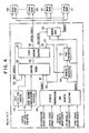
- Fig. 3 illustrates a typical system that the memory controller is used in.
- the system includes a number of sources of memory requests 100-104, a flexible memory controller 110, and a number of banks of memory 120-123.
- a microprocessor 100 generates memory requests in order to read and write memory as part of data update, instruction fetch, and other typical operations of a microprocessor. These requests are in the form of reads and writes, with a read request accompanied by its address, while a write request includes both the address and the data to be written at the address.
- a graphic assist engine 101 generates memory requests when drawing lines, performing BitBlts, setting and reading pixels, fetching display lists, etc. These requests are a combination of reads, writes, and read-modify-writes.
- a refresh controller 102 generates memory refresh requests. These are a special form of memory cycle wherein every DRAM/VRAM RAS line must be activated without a corresponding CAS cycle.
- a CRT controller 103 generates video refresh requests. These are a special form of memory cycle wherein a special line (typically called TR/QE) is activated prior to the start of the memory cycle to denote an internal row transfer cycle. These requests are valid only for VRAM.
- TR/QE special line
- Other devices 104 can generate memory reads, writes, or special cycles dependent on the device. Typical examples are a DMA controller, virtual memory manager, or a bus controller honoring requests from another bus.
- the flexible memory controller 110 recognizes requests from the various sources 100-104 and performs the desired memory operation.
- the memory controller 110 has the capability of controlling several types of dynamic random access memory and dual-port random access memory (typically called VRAM).
- Memory modules 120-123 are arranged in banks. Each bank of memory contains several modules such that a bank is a complete word plus other bits optionally present for error detection and correction (EDC). A typical width of a word in present day systems is 32 bits with 4 more bits for parity or 6-8 bits for EDC. Memory banks may be of different sizes dependent on the density of the underlying memory modules.
- EDC error detection and correction
- the bank sizes created with various density modules is as follows: o 256 K byte bank of 8 - 256 Kbit modules (64k x 4-bit) o 1 Mbyte bank of 32 - 256 Kbit modules (256K x 4-bit) o 1 Mbyte bank of 8 - 1 Mbit modules (256K x 4-bit) o 4 Mbyte bank of 32 - 1 Mbit modules (1M x 1-bit) o 4 Mbyte bank of 8 - 4 Mbit modules (1M x 4-bit) o 16 Mbyte bank of 32 - 4 Mbit modules (4M x 1-bit)
- Dynamic memory modules have been optimized by manufacturers in order to provide the highest possible performance and bandwidth.
- One form of optimization relates to various methods of page mode (page mode encompasses standard page mode, fast page mode, nibble mode, and static column mode).
- page mode encompasses standard page mode, fast page mode, nibble mode, and static column mode.
- a memory controller that can effectively use page mode is far more desirable and can provide a higher level of system performance.
- Fig. 4 is a detailed block diagram of the flexible memory controller 110 which functions as a sequential state machine.
- a request prioritization and address selector 200 receives all the memory requests from the various sources.
- the requests are prioritized by one of many schemes such as absolute fixed priority (requests are always ordered in the same manner from most urgent to least, rotating requests are given priority based on how long since last honored), age (requests are given priority based on how long the request has been active), or some combination of the above. What is relevant is that one and only one request (along with its address) passes through the prioritization section.
- a control store 240 which contains microcode describing the sequences the memory controller can perform.
- the control store may be any of a variety of technologies depending on the manner in which the flexible memory controller is realized. If the flexible memory controller is to be contained in a semi-custom chip such as a gate array, it may be composed of a plurality of logic gates such that the resulting logic gates match the desired input/output function of the control store. These gates may be the result of a logic reduction on the control store input/output function or its truth table.
- the control store can also be implemented in ROM (read only memory) on a semi-custom chip. If the flexible memory controller is implemented in a plurality of chips, then the control store may be composed of any of a number of commercially available ROMSs and PROMs.
- the control store based on an input address 300 coupled with the contents of state machine configuration registers 230 and various other inputs such as the requests 301, RAS down counter status 210, and page comparator 221 out on 302, generates output signals 303 that are then latched in state machine registers 241.
- RAS active time counter 210 and registers 230 receive control, data and address information (for loading their internal registers) from microprocessor 110. Details of the functions of these devices is described shortly.
- the output of the state machine registers 241 can be divided into three general categories: (1) feedback information on line 300 which are necessary to determine the next address for the control store 240, (2) memory control signals 304 for the memory banks, and (3) internal memory controller control signals 310 and 311 which are applied to multiplexor 250 and address register 220, respectively. It should be noted that memory control signals may be processed by conditioning logic before connecting to the memory modules.
- the previous address register 220 and page comparator 221 operate in concert to determine if the current memory request can be treated as a page-mode memory cycle.
- Fig. 5 is a detailed description of the page comparator 221.
- the page comparator 221 compares the bank and row address portion of the previous address stored in the address register 220 with the bank and row address portion of the current address from prioritization and address selection logic 200.
- the previous address was latched in the address register 220 at the beginning of the previous cycle, indicated on line 311.
- the row address portion varies depending on the size of the memory bank and whether or not banks are being interleaved.
- a top bits comparator 500 performs the comparison for all the bits above the page address plus bit 12 since they are common to all banks as either bank address bits or row address bits. Depending on the bank's memory modules, address bits 9, 10, and 11 must also match.
- EXCLUSIVE-NOR gates 510, 511, 512 output a ONE if the respective input address bits match, and a ZERO if there is no match. The output of these EXCLUSIVE-NOR gates are OR'd with the signals ignore address ⁇ 11>, ⁇ 10>, and ⁇ 9>. The resulting signals are all AND'd together with AND gates 530 and 540 to determine if there is page-mode address match.
- Determining the values of ignore address ⁇ 11>, ⁇ 10>, and ⁇ 9> may be a complicated matter dependent upon how many banks of memory there are and what kind of different modules are used (high order address bits need to be looked up in a table of some kind for this determination). However, careful examination reveals that by comparing ALL the top bits, the old values of ignore address ⁇ 11>, ⁇ 10>, and ⁇ 9> may be used. If the top address bits match, then also the correct bits, 11, 10, and 9 are checked for a match. If the top address bits don't match, then the comparator 500 will prevent a page-mode cycle. This allows a very fast comparison to be used without need for determining the "pro per" row address.
- the RAS active-time counter 210 prevents the memory controller from exceeding the maximum RAS active-time specification.
- dynamic memory modules specifications allow a limited duration of RAS active (page-mode operation) time. It is necessary to keep a count of how long RAS has been active in order to artificially bring the DRAM out of page-mode in the presence of a long string of page mode addresses.
- the counter is incremented every system clock cycle and compared to a preset value which is determined under control of the signal inputs from microprocessor 110.
- the maximum count is based on the speed of the system clock and the modules specification of maximum RAS active time (typically 10 microseconds). For a 24 MHz system clock, this translates into a maximum count of 240.
- the preset value is set lower than the number of clocks within the spec to allow for any memory operation to be completed. Continuing the previous example, if the longest memory cycle is 640 ns, then the maximum count is set to 224 - (10,000 ns - 640 ns/(1/24 MHz)) rounded down.
- the address multiplexor 250 allows the current address to be multiplexed into a row portion and a column portion.
- the multiplexor is 2N-way, with N equaling the number of different row/column address portions the various banks require.
- Control signals 304 include a separate RAS for each bank of RAM (260, 261, 270, 271), a set of CAS corresponding to the number of banks that can be interleaved (a set is composed of a separate CAS for each byte that can be individually written), write enable lines, TR/QE (for VRAM) lines, and output enable lines.
- the state machine configuration registers 230 provide inputs that can be tested for various conditions that can then modify the type of memory cycle to be performed. Changing the contents of the state machine configuration registers provides programmable memory cycles.
- the registers 230 respond to the signal inputs from microprocessor 100 which are indicative of the source of the memory request and the type of memory bank accessed, to change the contents of the registers.
- the control store 240 responds to the contents of the register 230 to change the duration of the cycle time of the control signals applied to the selected memory bank. Specifically the access time and precharge time of RAS and CAS are modified. This is described in detail relative to the flow charts of Figs. 7-10.
- the memory banks 260, 261, 270, and 271 can be two-way interleaved, such that banks 260 and 261 act as a pair, as do 270 and 271.
- Fig. 6 shows how control signals connect to banks of memory for two-way interleaving. These control signals are illustrated in Fig. 2.
- Each bank of memory has its own RAS line, there are (in this example) 4 CAS lines for each set of banks being interleaved (assuming byte selection for a 32-bit word), there are separate address and other control signals (WE, OE, etc.) for each set of banks being interleaved.
- Alternate addresses are stored in alternate banks, allowing faster access to a contiguous chunk of memory because access to the banks can be overlapped.
- An additional benefit of interleaving is that the page size is effectively doubled because now there is an active row in both banks. The page comparator must take this into account when comparing previous and current addresses.
- the flexible memory controller allows either DRAM interleaving, VRAM interleaving, both, or neither. In a typical system configuration, there will be more than one pair of memory banks, all of which can be interleaved. It is also possible to interleave more than two-way, however, current technology provides little benefit for the extra cost of separate CAS signals and internal control.
- Figs. 7 - 10 which illustrate the flowchart of the states the flexible dynamic memory controller can assume as manifested at the output of the state machine register 241 of Fig. 4.
- the changing of states is assumed to be based on an input clock to the state machine.
- This clock has a period (1/frequency) which determines how long a signal that is activated in one state and deactivated in a later state stays active.
- the initial state diagram flow is as set forth below.
- the initial state upon reset is the IDLE state 500 shown in Fig. 7. If a "regular" memory cycle request is detected (i.e. it flows through the request prioritization logic 200 of Fig. 4) then State 501 is entered, if a refresh request is detected then State 513 of Fig. 10 is entered via line 570. Other request types (such as a VRAM serial refresh request from CRT Controller) also branch off of State 500. When in State 501, the request address is decoded in order to determine which, and what type, bank is being accessed. If the bank being accessed is interleaved, then State 502 is entered, otherwise State 503 is entered.
- the non-selected bank's address is enabled (i.e. the odd bank in the case of an even bank request).
- the odd and even bank address buses, address A and address B lines of Fig. 6, must both have been enabled in the case of interleaved banks because the Row Address Strobes for both odd and even banks are activated together. Subsequent page mode cycles can then proceed in either the odd or the even bank.
- the address buses are not enabled together in order to minimize the number of simultaneously switched output pins. By enabling the address buses separately, higher power drivers can be utilized.
- the selected banks' address is enabled on either address A or address B line of Fig. 5 and then State 504 is entered.
- the Row Address Strobe (RAS) is activated for both odd and even banks, RAS A and RAS B of Fig. 2, if interleaved address or just the selected bank (odd or even) if the address is for a noninterleaved bank. RAS stays activated until state 512 is entered as shown in Fig. 9. If the clock period of the state machine is less than the row address hold time then state 506 follows state 504, otherwise state 507 (Fig. 7) follows state 504. While in State 506, no signals are changed, this allows extra time for the Row Address to be held after the falling edge of RAS, a parameter that is commonly specified in dynamic memory specifications.
- RAS Row Address Strobe
- state 507 the address is changed from the multiplexed row address to the column address.
- the Column Address Strobe (CAS) is activated. CAS remains activated until either State 511 (Fig. 9) or State 53n is reached.
- State 52n that is, State 521 or 522
- State 508 State 508
- State 509 follows state 508. While in State 52n, no signals are changed, this allows extra time for CAS access before the memory controller signals it has completed the memory cycle.
- the n in State 52n is the number of extra clock periods of access time that is needed. That is, if 1 extra clock cycle is needed, State 521 is entered, and if 2 extra clock cycles are needed, State 522 is entered. State 521 always follows State 522, and after State 521, State 509 is entered.
- State machine configuration registers 230 provide the inputs to control store 240 for determining CAS access time dynamically as a function of the source of memory request and the type of memory bank being accessed.
- CAS is held active and the memory controller returns DONE to the requester - in the case of a write the requester no longer needs to assert the data lines and in the case of a read the requester can now latch the memory data.
- CAS is held active if the active bank style is static column mode memory. Static column mode memory does not require CAS be brought inactive between page mode cycles. For static column mode memory banks, States 53n, that is States 531 and 532, are never entered.
- CAS precharge time is determined dynamically by control store 240 in response to input signals from registers 230 which are indicative of the source of the memory request and the type of memory bank being accessed. Assuming a page mode or fast-page mode memory bank is being accessed, there is a minimum CAS precharge time specification that must be met. If the minimum CAS precharge time is longer than the clock period then extra CAS precharge states need to be added. The default CAS precharge time is the time spent in one state, State 511. If extra CAS precharge time is required then State 53n (where n is the number of extra clock periods of CAS precharge time needed) follows State 509, otherwise State 511 follows State 509.
- State 531 is entered, and if 2 extra clock cycles are needed State 532 is entered. State 531 always follows State 532, and after State 531, State 511 is entered. If more than 2 extra CAS precharge states are required, State 533 is added ahead of State 532, State 534 is added ahead of 533, etc.
- Page Mode Idle is as follows. In State 511 several tests are performed every cycle. The highest priority test is the RAS active time count (from the RAS active time counter 210 of Fig. 4), if this count exceeds the programmed value then State 512, RAS Precharge, is entered. RAS access time and RAS precharge time, as previously set forth, are determined by control store 240 in accordance with input signals from registers 230 which are indicative of the source of the memory request and the type of memory bank being accessed. The second highest priority test is whether or not a request has occurred. If a request has not occurred, then the state machine stays in State 511. If, however, a request has come along, then the page comparator 221 (Fig.
- Control of delay CAS start is as follows. Some requesters require a delay of the CAS start in order to allow the requesting master extra time to generate data or parity when the request is a write. If the master needs extra time and State 508 (Fig. 8) would have normally followed State 511, then State 55n (where n is the number of extra clock periods required before the master is ready), follows instead. That is, if 1 extra clock cycle is required State 551 is entered and if 2 extra clock cycles are required State 552 is entered. State 551 always follows State 552, and after State 551, State 508 is entered. If more than 2 extra delay states are required, State 553 is added ahead of State 552, State 554 is added ahead of 553, etc.
- Control of RAS precharge time is as follows. If the minimum RAS precharge time is longer than three clock periods (the time in State 512, 501, and 503) then extra RAS precharge states need to be added. If extra RAS precharge time is required then State 54n (where n is the number of extra clock periods of precharge time needed) follows State 512, otherwise either State 500 (no request pending) or State 501 (request pending) follows State 512. That is, if 1 extra clock cycle is required State 541 is entered and if 2 extra clock cycles are required State 542 is entered. State 541 always follows State 542, and after State 541, State 500 or State 501 is entered (again, depending on a pending request). If more than 2 extra RAS precharge states are required, State 543 is added ahead of State 542, State 544 is added ahead of 543, etc.
- control of refresh RAS active time is as follows. Whenever a refresh request is detected State 513 is entered after the previous cycle is completed (State 541 or State 512 of Fig. 9) or from IDLE. In State 513, the refresh address is enabled onto the odd address bus and then State 514 is entered. In State 514, the refresh address is enabled onto the even address bus and then State 515 is entered. In State 515 RAS is activated to all banks of memory. If the clock period of the state machine is less than the minimum time then State 56n, where n is the number of extra clock periods of RAS active time needed, follows state 515, otherwise State 512 follows State 515.
- State 561 if 1 extra clock cycle is required State 561 is entered, if 2 extra clock cycles are required State 562 is entered, and if 3 extra clock cycles are required Sate 563 is entered. While in State 56n, no signals are changed, this allows extra time for refresh RAS time before RAS is deactivated. State 562 always follows State 563, State 561 always follows State 562, and after State 561, State 512 is entered.
- State 564 is added ahead of State 563, State 565 is added ahead of 564, etc.
- Refresh minimum RAS time is commonly specified in dynamic memory specifications and is usually the same as the RAS access time.
- n for State 5xn selection is as set forth below.
- the preceding analysis of the state flowchart contained several references to a value n where n is the extra RAS precharge time or the extra CAS access time, etc.
- the state machine configuration registers 230 (Fig. 4) contain the relevant n value for each desired attribute.
- Table 2 shows example attribute values.
- the Table 2 can be stored in a series of registers comprising registers 230.
- TABLE 2 BANK SPECIFIC PARAMETERS Parameter States Bank A Bank B Bank C Bank D CAS Access Time 52n 0 0 1 0 CAS Precharge Time 53n 0 0 1 1 RAS Precharge Time 54n 1 1 2 2 RAS Access Time 56n 2 2 3 3 Row Address Hold Time 506 no no yes no Static Column Mode no no yes no Interleaved yes yes no no no REQUESTING MASTER PARAMETERS Parameter States Microprocessor Graphic Assist Engine Refresh Controller CRT Controller CAS Delay Time 55n 1 0 0 0 0
- State 500 State 500
- State 501 State 502 (since A is interleaved)
- State 503 State 504, State 507, State 508, State 509, State 511, and then after no request and a timeout - State 512, State 541, State 500.
- State 500 State 500, State 501, State 503, State 504, State 506, State 507, State 508, State 521, State 509, State 531, State 511, State 512, State 542, State 541, State 501, State 503, State 504, State 506, State 507, State 508, State 521, State 509, State 531, State 511, and then after no request and a timeout - State 512, State 542, State 541, State 500.
- State 500 State 513, State 514, State 515, State 563 (longest of RAS access is chosen), State 562, State 561, State 512, State 542, State 541, State 500.
- a memory controller which responds to memory access requests from a plurality of different processors to provide control signals to a plurality of memory banks which may have different cycle times of operation.
- the duration of the cycle time of the control signals is dynamically determined as a function of the source of the memory request and the type of memory bank accessed.
Applications Claiming Priority (2)
| Application Number | Priority Date | Filing Date | Title |
|---|---|---|---|
| US18770688A | 1988-04-29 | 1988-04-29 | |
| US187706 | 1988-04-29 |
Publications (2)
| Publication Number | Publication Date |
|---|---|
| EP0339224A2 true EP0339224A2 (en) | 1989-11-02 |
| EP0339224A3 EP0339224A3 (en) | 1992-04-01 |
Family
ID=22690123
Family Applications (1)
| Application Number | Title | Priority Date | Filing Date |
|---|---|---|---|
| EP19890104268 Withdrawn EP0339224A3 (en) | 1988-04-29 | 1989-03-10 | Memory controller |
Country Status (2)
| Country | Link |
|---|---|
| EP (1) | EP0339224A3 (un) |
| JP (1) | JPH0212541A (un) |
Cited By (32)
| Publication number | Priority date | Publication date | Assignee | Title |
|---|---|---|---|---|
| EP0549139A1 (en) * | 1991-12-20 | 1993-06-30 | Sun Microsystems, Inc. | Programmable memory timing |
| WO1993020560A1 (en) * | 1992-03-31 | 1993-10-14 | Digital Equipment Corporation | High-density double-sided multi-string memory module |
| EP0580961A1 (en) * | 1992-07-17 | 1994-02-02 | International Business Machines Corporation | An enhanced processor buffered interface for multiprocessor systems |
| EP0617365A1 (en) * | 1993-03-22 | 1994-09-28 | Compaq Computer Corporation | Fully pipelined and highly concurrent memory controller |
| WO1994025914A2 (en) * | 1993-04-30 | 1994-11-10 | Zenith Data Systems Corporation | Symmetric multiprocessing system with unified environment and distributed system functions |
| EP0624846A2 (en) * | 1993-05-14 | 1994-11-17 | Sony Corporation | Bus control apparatus |
| EP0707268A3 (en) * | 1994-10-14 | 1996-07-31 | Compaq Computer Corp | Easily programmable memory control which can access memory devices of different speeds in different cycles |
| EP0690370A3 (en) * | 1994-06-30 | 1997-04-23 | Softchip Israel Ltd | Microprocessor device and peripheral devices |
| WO1997014289A2 (en) * | 1995-10-19 | 1997-04-24 | Rambus, Inc. | Protocol for communication with dynamic memory |
| GB2308475A (en) * | 1995-12-22 | 1997-06-25 | Memory Corp Plc | Delaying reading of memory comprising chips having dissimilar access times to ensure validity of data read |
| EP0797152A1 (en) * | 1996-03-22 | 1997-09-24 | Matsushita Electric Industrial Co., Ltd. | Single-chip microcomputer with memory controller |
| EP0809252A2 (en) * | 1992-09-18 | 1997-11-26 | Hitachi, Ltd. | Data processing system with synchronous dynamic memory in integrated circuit technology |
| WO1998015897A1 (en) * | 1996-10-10 | 1998-04-16 | Hewlett-Packard Company | Memory system and device |
| WO1998055935A1 (en) * | 1997-06-04 | 1998-12-10 | Oak Technology, Inc. | Apparatus and method for reading data from synchronous memory at increased system clock frequencies |
| EP0926599A1 (en) * | 1997-12-24 | 1999-06-30 | BULL HN INFORMATION SYSTEMS ITALIA S.p.A. | Memory control unit with programmable timing |
| EP0932105A2 (en) * | 1998-01-22 | 1999-07-28 | Matsushita Electric Industrial Co., Ltd. | Memory access controller |
| EP0955639A2 (en) * | 1998-05-07 | 1999-11-10 | Kabushiki Kaisha Toshiba | Semiconductor memory system, and access control method for semiconductor memory and semiconductor memory |
| EP0973167A2 (en) * | 1998-07-17 | 2000-01-19 | Kabushiki Kaisha Toshiba | High-speed cycle clock-synchronous memory device |
| WO2000020978A1 (en) * | 1998-10-02 | 2000-04-13 | International Business Machines Corporation | Memory controller with programmable delay counter for tuning performance based on timing parameter of controlled memory storage device |
| US6470405B2 (en) | 1995-10-19 | 2002-10-22 | Rambus Inc. | Protocol for communication with dynamic memory |
| US6519716B1 (en) | 1999-09-22 | 2003-02-11 | International Business Machines Corporation | Electronic device initialization with dynamic selection of access time for non-volatile memory |
| US6591353B1 (en) | 1995-10-19 | 2003-07-08 | Rambus Inc. | Protocol for communication with dynamic memory |
| FR2844613A1 (fr) * | 2002-09-13 | 2004-03-19 | Hewlett Packard Development Co | Systeme pour le transfert rapide des donnees |
| EP1437660A2 (en) * | 2002-12-27 | 2004-07-14 | Nec Corporation | Semiconductor memory device and mount-type semiconductor device |
| EP1640847A2 (en) * | 1990-04-18 | 2006-03-29 | Rambus, Inc. | Dynamic random access memory (DRAM) semiconductor device |
| WO2006058200A2 (en) | 2004-11-29 | 2006-06-01 | Rambus Inc. | Micro-threaded memory |
| US7793039B2 (en) | 1997-10-10 | 2010-09-07 | Rambus Inc. | Interface for a semiconductor memory device and method for controlling the interface |
| US7870357B2 (en) | 1997-10-10 | 2011-01-11 | Rambus Inc. | Memory system and method for two step memory write operations |
| US8238470B2 (en) | 1997-06-20 | 2012-08-07 | Massachusetts Institute Of Technology | Digital transmitter |
| US8364926B2 (en) | 2006-05-02 | 2013-01-29 | Rambus Inc. | Memory module with reduced access granularity |
| US8432766B2 (en) | 2004-09-30 | 2013-04-30 | Rambus Inc. | Multi-column addressing mode memory system including an integrated circuit memory device |
| US9268719B2 (en) | 2011-08-05 | 2016-02-23 | Rambus Inc. | Memory signal buffers and modules supporting variable access granularity |
Families Citing this family (2)
| Publication number | Priority date | Publication date | Assignee | Title |
|---|---|---|---|---|
| WO2001059573A1 (fr) * | 2000-02-07 | 2001-08-16 | Hitachi, Ltd. | Dispositif de traitement de l'information et circuit integre a semi-conducteurs |
| US7477257B2 (en) * | 2005-12-15 | 2009-01-13 | Nvidia Corporation | Apparatus, system, and method for graphics memory hub |
Citations (3)
| Publication number | Priority date | Publication date | Assignee | Title |
|---|---|---|---|---|
| JPS52149037A (en) * | 1976-06-04 | 1977-12-10 | Hitachi Ltd | Control circuit of memory containing plural kinds of memory element |
| JPS5856276A (ja) * | 1981-09-30 | 1983-04-02 | Fujitsu Ltd | 記憶装置制御方式 |
| EP0245882A2 (en) * | 1986-05-12 | 1987-11-19 | Advanced Micro Devices, Inc. | Data processing system including dynamic random access memory controller with multiple independent control channels |
Family Cites Families (1)
| Publication number | Priority date | Publication date | Assignee | Title |
|---|---|---|---|---|
| JPS6035691B2 (ja) * | 1980-01-14 | 1985-08-16 | 株式会社日立製作所 | 情報処理装置 |
-
1989
- 1989-01-20 JP JP1009789A patent/JPH0212541A/ja active Pending
- 1989-03-10 EP EP19890104268 patent/EP0339224A3/en not_active Withdrawn
Patent Citations (3)
| Publication number | Priority date | Publication date | Assignee | Title |
|---|---|---|---|---|
| JPS52149037A (en) * | 1976-06-04 | 1977-12-10 | Hitachi Ltd | Control circuit of memory containing plural kinds of memory element |
| JPS5856276A (ja) * | 1981-09-30 | 1983-04-02 | Fujitsu Ltd | 記憶装置制御方式 |
| EP0245882A2 (en) * | 1986-05-12 | 1987-11-19 | Advanced Micro Devices, Inc. | Data processing system including dynamic random access memory controller with multiple independent control channels |
Non-Patent Citations (2)
| Title |
|---|
| PATENT ABSTRACTS OF JAPAN vol. 002, no. 027 (E-16)21 February 1978 & JP-A-52 149 037 ( HITACHI SEISAKUSHO KK ) 12 October 1977 * |
| PATENT ABSTRACTS OF JAPAN vol. 7, no. 146 (P-206)(1291) 25 June 1983 & JP-A-58 056 276 ( FUJITSU LIMITED ) 2 April 1983 * |
Cited By (104)
| Publication number | Priority date | Publication date | Assignee | Title |
|---|---|---|---|---|
| EP1640847A2 (en) * | 1990-04-18 | 2006-03-29 | Rambus, Inc. | Dynamic random access memory (DRAM) semiconductor device |
| EP1640847A3 (en) * | 1990-04-18 | 2006-05-31 | Rambus, Inc. | Dynamic random access memory (DRAM) semiconductor device |
| EP1816569A3 (en) * | 1990-04-18 | 2007-09-26 | Rambus Inc. | Integrated circuit I/O using a high performance bus interface |
| US5394541A (en) * | 1990-07-17 | 1995-02-28 | Sun Microsystems, Inc. | Programmable memory timing method and apparatus for programmably generating generic and then type specific memory timing signals |
| EP0549139A1 (en) * | 1991-12-20 | 1993-06-30 | Sun Microsystems, Inc. | Programmable memory timing |
| WO1993020560A1 (en) * | 1992-03-31 | 1993-10-14 | Digital Equipment Corporation | High-density double-sided multi-string memory module |
| EP0580961A1 (en) * | 1992-07-17 | 1994-02-02 | International Business Machines Corporation | An enhanced processor buffered interface for multiprocessor systems |
| US5634034A (en) * | 1992-07-17 | 1997-05-27 | International Business Machines Corporation | Enhanced processor buffered interface for multiprocess systems |
| US7376783B2 (en) | 1992-09-18 | 2008-05-20 | Renesas Technology Corp. | Processor system using synchronous dynamic memory |
| EP0809252A3 (en) * | 1992-09-18 | 1998-04-01 | Hitachi, Ltd. | Data processing system with synchronous dynamic memory in integrated circuit technology |
| US6260107B1 (en) | 1992-09-18 | 2001-07-10 | Hitachi, Ltd | Processor system using synchronous dynamic memory |
| US6334166B1 (en) | 1992-09-18 | 2001-12-25 | Hitachi, Ltd. | Processor system using synchronous dynamic memory |
| US8234441B2 (en) | 1992-09-18 | 2012-07-31 | Renesas Electronics Corporation | Processor system using synchronous dynamic memory |
| US6697908B2 (en) | 1992-09-18 | 2004-02-24 | Renesas Technology Corporation | Processor system using synchronous dynamic memory |
| US6078986A (en) * | 1992-09-18 | 2000-06-20 | Hitachi, Ltd. | Processor system using synchronous dynamic memory |
| US7143230B2 (en) | 1992-09-18 | 2006-11-28 | Renesas Technology Corp. | Processor system using synchronous dynamic memory |
| EP0809252A2 (en) * | 1992-09-18 | 1997-11-26 | Hitachi, Ltd. | Data processing system with synchronous dynamic memory in integrated circuit technology |
| US5537555A (en) * | 1993-03-22 | 1996-07-16 | Compaq Computer Corporation | Fully pipelined and highly concurrent memory controller |
| EP0617365A1 (en) * | 1993-03-22 | 1994-09-28 | Compaq Computer Corporation | Fully pipelined and highly concurrent memory controller |
| WO1994025914A3 (en) * | 1993-04-30 | 1995-01-05 | Zenith Data Systems Corp | Symmetric multiprocessing system with unified environment and distributed system functions |
| WO1994025914A2 (en) * | 1993-04-30 | 1994-11-10 | Zenith Data Systems Corporation | Symmetric multiprocessing system with unified environment and distributed system functions |
| US5682555A (en) * | 1993-05-14 | 1997-10-28 | Sony Corp | Bus control apparatus |
| EP0624846A2 (en) * | 1993-05-14 | 1994-11-17 | Sony Corporation | Bus control apparatus |
| EP0624846A3 (en) * | 1993-05-14 | 1995-01-18 | Sony Corp | Bus control device. |
| US5935428A (en) * | 1993-05-14 | 1999-08-10 | Sony Corporation | Apparatus and method for performing efficient read and write operations in a multiple bus system |
| US5729766A (en) * | 1994-06-30 | 1998-03-17 | Softchip Israel Ltd. | System for memory unit receiving pseudo-random delay signal operative to access memory after delay and additional delay signal extending from termination of memory access |
| EP0690370A3 (en) * | 1994-06-30 | 1997-04-23 | Softchip Israel Ltd | Microprocessor device and peripheral devices |
| US5778413A (en) * | 1994-10-14 | 1998-07-07 | Compaq Computer Corporation | Programmable memory controller having two level look-up for memory timing parameter |
| AU703750B2 (en) * | 1994-10-14 | 1999-04-01 | Compaq Computer Corporation | Easily programmable memory controller which can access different speed memory devices on different cycles |
| EP0707268A3 (en) * | 1994-10-14 | 1996-07-31 | Compaq Computer Corp | Easily programmable memory control which can access memory devices of different speeds in different cycles |
| US6591353B1 (en) | 1995-10-19 | 2003-07-08 | Rambus Inc. | Protocol for communication with dynamic memory |
| WO1997014289A2 (en) * | 1995-10-19 | 1997-04-24 | Rambus, Inc. | Protocol for communication with dynamic memory |
| US6931467B2 (en) | 1995-10-19 | 2005-08-16 | Rambus Inc. | Memory integrated circuit device which samples data upon detection of a strobe signal |
| US5748914A (en) * | 1995-10-19 | 1998-05-05 | Rambus, Inc. | Protocol for communication with dynamic memory |
| US5913046A (en) * | 1995-10-19 | 1999-06-15 | Rambus Inc. | Protocol for communication with dynamic memory |
| WO1997014289A3 (en) * | 1995-10-19 | 1998-04-02 | Rambus Inc | Protocol for communication with dynamic memory |
| US6810449B1 (en) | 1995-10-19 | 2004-10-26 | Rambus, Inc. | Protocol for communication with dynamic memory |
| US5966731A (en) * | 1995-10-19 | 1999-10-12 | Rambus, Inc. | Protocol for communication with dynamic memory |
| US6470405B2 (en) | 1995-10-19 | 2002-10-22 | Rambus Inc. | Protocol for communication with dynamic memory |
| GB2308475A (en) * | 1995-12-22 | 1997-06-25 | Memory Corp Plc | Delaying reading of memory comprising chips having dissimilar access times to ensure validity of data read |
| US6023776A (en) * | 1996-03-22 | 2000-02-08 | Matsushita Electric Industrial Co., Ltd. | Central processing unit having a register which store values to vary wait cycles |
| EP0797152A1 (en) * | 1996-03-22 | 1997-09-24 | Matsushita Electric Industrial Co., Ltd. | Single-chip microcomputer with memory controller |
| WO1998015897A1 (en) * | 1996-10-10 | 1998-04-16 | Hewlett-Packard Company | Memory system and device |
| US6131149A (en) * | 1997-06-04 | 2000-10-10 | Oak Technology, Inc. | Apparatus and method for reading data from synchronous memory with skewed clock pulses |
| WO1998055935A1 (en) * | 1997-06-04 | 1998-12-10 | Oak Technology, Inc. | Apparatus and method for reading data from synchronous memory at increased system clock frequencies |
| US8243847B2 (en) | 1997-06-20 | 2012-08-14 | Massachusetts Institute Of Technology | Digital transmitter |
| US8238470B2 (en) | 1997-06-20 | 2012-08-07 | Massachusetts Institute Of Technology | Digital transmitter |
| US8761235B2 (en) | 1997-06-20 | 2014-06-24 | Massachusetts Institute Of Technology | Digital transmitter |
| US8238467B2 (en) | 1997-06-20 | 2012-08-07 | Massachusetts Institute Of Technology | Digital transmitter |
| US8923433B2 (en) | 1997-06-20 | 2014-12-30 | Massachusetts Institute Of Technology | Digital transmitter |
| US8681837B2 (en) | 1997-06-20 | 2014-03-25 | Massachusetts Institute Of Technology | Digital Transmitter |
| US8989303B2 (en) | 1997-06-20 | 2015-03-24 | Massachusetts Institute Of Technology | Digital transmitter |
| US9419824B2 (en) | 1997-06-20 | 2016-08-16 | Massachusetts Institute Of Technology | Digital transmitter |
| US8254491B2 (en) | 1997-06-20 | 2012-08-28 | Massachusetts Institute Of Technology | Digital transmitter |
| US8259841B2 (en) | 1997-06-20 | 2012-09-04 | Massachusetts Institute Of Technology | Digital transmitter |
| US8311147B2 (en) | 1997-06-20 | 2012-11-13 | Massachusetts Institute Of Technology | Digital transmitter |
| US9647857B2 (en) | 1997-06-20 | 2017-05-09 | Massachusetts Institute Of Technology | Digital transmitter |
| US8560797B2 (en) | 1997-10-10 | 2013-10-15 | Rambus Inc. | Method and apparatus for indicating mask information |
| US7793039B2 (en) | 1997-10-10 | 2010-09-07 | Rambus Inc. | Interface for a semiconductor memory device and method for controlling the interface |
| US8140805B2 (en) | 1997-10-10 | 2012-03-20 | Rambus Inc. | Memory component having write operation with multiple time periods |
| US8019958B2 (en) | 1997-10-10 | 2011-09-13 | Rambus Inc. | Memory write signaling and methods thereof |
| US8205056B2 (en) | 1997-10-10 | 2012-06-19 | Rambus Inc. | Memory controller for controlling write signaling |
| US7870357B2 (en) | 1997-10-10 | 2011-01-11 | Rambus Inc. | Memory system and method for two step memory write operations |
| US8504790B2 (en) | 1997-10-10 | 2013-08-06 | Rambus Inc. | Memory component having write operation with multiple time periods |
| EP0926599A1 (en) * | 1997-12-24 | 1999-06-30 | BULL HN INFORMATION SYSTEMS ITALIA S.p.A. | Memory control unit with programmable timing |
| EP0932105A2 (en) * | 1998-01-22 | 1999-07-28 | Matsushita Electric Industrial Co., Ltd. | Memory access controller |
| EP0932105A3 (en) * | 1998-01-22 | 2002-05-29 | Matsushita Electric Industrial Co., Ltd. | Memory access controller |
| US6442088B1 (en) | 1998-05-07 | 2002-08-27 | Kabushiki Kaisha Toshiba | Semiconductor memory system, and access control method for semiconductor memory and semiconductor memory |
| US6335904B1 (en) | 1998-05-07 | 2002-01-01 | Kabushiki Kaisha Toshiba | Semiconductor memory system, and access control method for semiconductor memory and semiconductor memory |
| EP0955639A2 (en) * | 1998-05-07 | 1999-11-10 | Kabushiki Kaisha Toshiba | Semiconductor memory system, and access control method for semiconductor memory and semiconductor memory |
| US6256258B1 (en) | 1998-05-07 | 2001-07-03 | Kabushiki Kaisha Toshiba | Semiconductor memory system, and access control method for semiconductor memory and semiconductor memory |
| EP0955639A3 (en) * | 1998-05-07 | 2000-05-10 | Kabushiki Kaisha Toshiba | Semiconductor memory system, and access control method for semiconductor memory and semiconductor memory |
| US6295231B1 (en) | 1998-07-17 | 2001-09-25 | Kabushiki Kaisha Toshiba | High-speed cycle clock-synchronous memory device |
| US6556507B2 (en) | 1998-07-17 | 2003-04-29 | Kabushiki Kaisha Toshiba | High-speed cycle clock-synchrounous memory device |
| EP0973167A2 (en) * | 1998-07-17 | 2000-01-19 | Kabushiki Kaisha Toshiba | High-speed cycle clock-synchronous memory device |
| US6480423B2 (en) | 1998-07-17 | 2002-11-12 | Kabushiki Kaisha Toshiba | High-speed cycle clock-synchronous memory device |
| EP0973167A3 (en) * | 1998-07-17 | 2000-05-17 | Kabushiki Kaisha Toshiba | High-speed cycle clock-synchronous memory device |
| WO2000020978A1 (en) * | 1998-10-02 | 2000-04-13 | International Business Machines Corporation | Memory controller with programmable delay counter for tuning performance based on timing parameter of controlled memory storage device |
| US6438670B1 (en) | 1998-10-02 | 2002-08-20 | International Business Machines Corporation | Memory controller with programmable delay counter for tuning performance based on timing parameter of controlled memory storage device |
| KR100450726B1 (ko) * | 1998-10-02 | 2004-10-01 | 인터내셔널 비지네스 머신즈 코포레이션 | 제어된 메모리 저장 장치의 타이밍 파라미터를 토대로 하여 실행 능력을 조절하기 위한 프로그램 가능 지연 카운터를 갖는 메모리 컨트롤러 |
| US6453434B2 (en) | 1998-10-02 | 2002-09-17 | International Business Machines Corporation | Dynamically-tunable memory controller |
| US6519716B1 (en) | 1999-09-22 | 2003-02-11 | International Business Machines Corporation | Electronic device initialization with dynamic selection of access time for non-volatile memory |
| US7111142B2 (en) | 2002-09-13 | 2006-09-19 | Seagate Technology Llc | System for quickly transferring data |
| FR2844613A1 (fr) * | 2002-09-13 | 2004-03-19 | Hewlett Packard Development Co | Systeme pour le transfert rapide des donnees |
| EP1437660A3 (en) * | 2002-12-27 | 2006-10-04 | Nec Corporation | Semiconductor memory device and mount-type semiconductor device |
| EP1437660A2 (en) * | 2002-12-27 | 2004-07-14 | Nec Corporation | Semiconductor memory device and mount-type semiconductor device |
| US8908466B2 (en) | 2004-09-30 | 2014-12-09 | Rambus Inc. | Multi-column addressing mode memory system including an integrated circuit memory device |
| US8432766B2 (en) | 2004-09-30 | 2013-04-30 | Rambus Inc. | Multi-column addressing mode memory system including an integrated circuit memory device |
| US9292223B2 (en) | 2004-11-29 | 2016-03-22 | Rambus Inc. | Micro-threaded memory |
| EP1820195B1 (en) * | 2004-11-29 | 2016-08-17 | Rambus Inc. | Micro-threaded memory |
| US8595459B2 (en) | 2004-11-29 | 2013-11-26 | Rambus Inc. | Micro-threaded memory |
| US10331379B2 (en) | 2004-11-29 | 2019-06-25 | Rambus Inc. | Memory controller for micro-threaded memory operations |
| WO2006058200A2 (en) | 2004-11-29 | 2006-06-01 | Rambus Inc. | Micro-threaded memory |
| EP1820195A2 (en) * | 2004-11-29 | 2007-08-22 | Rambus, Inc. | Micro-threaded memory |
| EP2363858A3 (en) * | 2004-11-29 | 2012-04-25 | Rambus Inc. | Multi-bank memory with interleaved or parallel accesses of banks |
| US11797227B2 (en) | 2004-11-29 | 2023-10-24 | Rambus Inc. | Memory controller for micro-threaded memory operations |
| US9652176B2 (en) | 2004-11-29 | 2017-05-16 | Rambus Inc. | Memory controller for micro-threaded memory operations |
| US8364926B2 (en) | 2006-05-02 | 2013-01-29 | Rambus Inc. | Memory module with reduced access granularity |
| US11467986B2 (en) | 2006-05-02 | 2022-10-11 | Rambus Inc. | Memory controller for selective rank or subrank access |
| US10191866B2 (en) | 2006-05-02 | 2019-01-29 | Rambus Inc. | Memory controller for selective rank or subrank access |
| US9256557B2 (en) | 2006-05-02 | 2016-02-09 | Rambus Inc. | Memory controller for selective rank or subrank access |
| US10795834B2 (en) | 2006-05-02 | 2020-10-06 | Rambus Inc. | Memory controller for selective rank or subrank access |
| US9268719B2 (en) | 2011-08-05 | 2016-02-23 | Rambus Inc. | Memory signal buffers and modules supporting variable access granularity |
| US9666250B2 (en) | 2011-08-05 | 2017-05-30 | Rambus Inc. | Memory signal buffers and modules supporting variable access granularity |
Also Published As
| Publication number | Publication date |
|---|---|
| JPH0212541A (ja) | 1990-01-17 |
| EP0339224A3 (en) | 1992-04-01 |
Similar Documents
| Publication | Publication Date | Title |
|---|---|---|
| US5301278A (en) | Flexible dynamic memory controller | |
| EP0339224A2 (en) | Memory controller | |
| US5966727A (en) | Combination flash memory and dram memory board interleave-bypass memory access method, and memory access device incorporating both the same | |
| US6021477A (en) | Multiple mode memory module | |
| US6721864B2 (en) | Programmable memory controller | |
| US5239642A (en) | Data processor with shared control and drive circuitry for both breakpoint and content addressable storage devices | |
| US5826093A (en) | Dual function disk drive integrated circuit for master mode and slave mode operations | |
| EP0622737A2 (en) | High performance memory system | |
| US5307469A (en) | Multiple mode memory module | |
| US6725349B2 (en) | Method and apparatus for controlling of a memory subsystem installed with standard page mode memory and an extended data out memory | |
| US4903197A (en) | Memory bank selection arrangement generating first bits identifying a bank of memory and second bits addressing identified bank | |
| EP0590967B1 (en) | Wait-state control in an information processing system bus | |
| US5901298A (en) | Method for utilizing a single multiplex address bus between DRAM, SRAM and ROM | |
| JPH08221319A (ja) | 半導体記憶装置 | |
| US7310717B2 (en) | Data transfer control unit with selectable transfer unit size | |
| EP1262988A2 (en) | Embedded memory access method and system for application specific integrated circuits | |
| US5751998A (en) | Memory accessing system with portions of memory being selectively write protectable and relocatable based on predefined register bits and memory selection RAM outputs | |
| US6292867B1 (en) | Data processing system | |
| US6564308B2 (en) | Multiple mode memory module | |
| US5684979A (en) | Method and means for initializing a page mode memory in a computer | |
| EP0619546A1 (en) | Programmable memory controller and method for configuring same | |
| EP0426386A2 (en) | Data destination facility | |
| US6141727A (en) | Device and method for controlling data storage device | |
| KR970010367B1 (ko) | 멀티프로세서 시스템에서 주기억장치의 보드내 인터리빙 장치 및 방법 | |
| JPH0333951A (ja) | マイクロコンピュータシステム |
Legal Events
| Date | Code | Title | Description |
|---|---|---|---|
| PUAI | Public reference made under article 153(3) epc to a published international application that has entered the european phase |
Free format text: ORIGINAL CODE: 0009012 |
|
| AK | Designated contracting states |
Kind code of ref document: A2 Designated state(s): DE FR GB |
|
| 17P | Request for examination filed |
Effective date: 19900224 |
|
| PUAL | Search report despatched |
Free format text: ORIGINAL CODE: 0009013 |
|
| AK | Designated contracting states |
Kind code of ref document: A3 Designated state(s): DE FR GB |
|
| 17Q | First examination report despatched |
Effective date: 19930330 |
|
| STAA | Information on the status of an ep patent application or granted ep patent |
Free format text: STATUS: THE APPLICATION IS DEEMED TO BE WITHDRAWN |
|
| 18D | Application deemed to be withdrawn |
Effective date: 19930810 |