EP0342201B1 - Electronic sensing apparatus for measuring projectile parameters - Google Patents
Electronic sensing apparatus for measuring projectile parameters Download PDFInfo
- Publication number
- EP0342201B1 EP0342201B1 EP88902282A EP88902282A EP0342201B1 EP 0342201 B1 EP0342201 B1 EP 0342201B1 EP 88902282 A EP88902282 A EP 88902282A EP 88902282 A EP88902282 A EP 88902282A EP 0342201 B1 EP0342201 B1 EP 0342201B1
- Authority
- EP
- European Patent Office
- Prior art keywords
- data
- electronic
- detecting
- radiation
- digital signals
- Prior art date
- Legal status (The legal status is an assumption and is not a legal conclusion. Google has not performed a legal analysis and makes no representation as to the accuracy of the status listed.)
- Expired
Links
- 239000000872 buffer Substances 0.000 claims description 32
- 230000003321 amplification Effects 0.000 claims description 24
- 238000003199 nucleic acid amplification method Methods 0.000 claims description 24
- 230000005855 radiation Effects 0.000 claims description 23
- 238000001514 detection method Methods 0.000 claims description 21
- 238000000034 method Methods 0.000 claims description 12
- 239000000835 fiber Substances 0.000 claims description 9
- 238000012545 processing Methods 0.000 claims description 6
- 238000006243 chemical reaction Methods 0.000 claims 6
- 239000006185 dispersion Substances 0.000 abstract description 7
- 238000005259 measurement Methods 0.000 abstract description 7
- 230000035939 shock Effects 0.000 abstract description 6
- 238000010586 diagram Methods 0.000 description 13
- 230000010354 integration Effects 0.000 description 13
- 238000012360 testing method Methods 0.000 description 13
- 230000003287 optical effect Effects 0.000 description 11
- 238000012546 transfer Methods 0.000 description 11
- 238000003491 array Methods 0.000 description 10
- 238000010304 firing Methods 0.000 description 7
- 230000006870 function Effects 0.000 description 7
- 238000004458 analytical method Methods 0.000 description 5
- 239000003990 capacitor Substances 0.000 description 5
- 230000001143 conditioned effect Effects 0.000 description 5
- 230000003068 static effect Effects 0.000 description 5
- 230000008859 change Effects 0.000 description 4
- 230000009467 reduction Effects 0.000 description 4
- 230000008901 benefit Effects 0.000 description 3
- 230000005540 biological transmission Effects 0.000 description 3
- 238000012986 modification Methods 0.000 description 3
- 230000004048 modification Effects 0.000 description 3
- 206010065929 Cardiovascular insufficiency Diseases 0.000 description 2
- 230000004075 alteration Effects 0.000 description 2
- 238000011982 device technology Methods 0.000 description 2
- 230000000694 effects Effects 0.000 description 2
- 230000007613 environmental effect Effects 0.000 description 2
- 230000004044 response Effects 0.000 description 2
- 238000005070 sampling Methods 0.000 description 2
- 238000009825 accumulation Methods 0.000 description 1
- 238000012937 correction Methods 0.000 description 1
- 238000007405 data analysis Methods 0.000 description 1
- 238000013479 data entry Methods 0.000 description 1
- 230000001419 dependent effect Effects 0.000 description 1
- 238000013461 design Methods 0.000 description 1
- 230000009977 dual effect Effects 0.000 description 1
- 238000000605 extraction Methods 0.000 description 1
- 230000010006 flight Effects 0.000 description 1
- 230000006872 improvement Effects 0.000 description 1
- 238000000691 measurement method Methods 0.000 description 1
- 230000005055 memory storage Effects 0.000 description 1
- 239000000203 mixture Substances 0.000 description 1
- 239000013307 optical fiber Substances 0.000 description 1
- 230000008569 process Effects 0.000 description 1
- 230000035945 sensitivity Effects 0.000 description 1
- 239000007787 solid Substances 0.000 description 1
- 230000003595 spectral effect Effects 0.000 description 1
- 230000001960 triggered effect Effects 0.000 description 1
Images


Classifications
-
- G—PHYSICS
- G01—MEASURING; TESTING
- G01P—MEASURING LINEAR OR ANGULAR SPEED, ACCELERATION, DECELERATION, OR SHOCK; INDICATING PRESENCE, ABSENCE, OR DIRECTION, OF MOVEMENT
- G01P3/00—Measuring linear or angular speed; Measuring differences of linear or angular speeds
- G01P3/64—Devices characterised by the determination of the time taken to traverse a fixed distance
- G01P3/68—Devices characterised by the determination of the time taken to traverse a fixed distance using optical means, i.e. using infrared, visible, or ultraviolet light
- G01P3/685—Devices characterised by the determination of the time taken to traverse a fixed distance using optical means, i.e. using infrared, visible, or ultraviolet light for projectile velocity measurements
Definitions
- the present invention relates to an electronic sensing apparatus according to the preamble of claim 1 or 3 and to a method for measuring various parameters of moving projectiles according to the preamble of claim 8.
- US-A-3 727 069 shows a system for measuring the location and diameter of a projectile in a frame of reference which includes vertical and horizontal banks of light sources for projecting collimated beams of light across the target area and corresponding vertical and horizontal banks of light receptors for indicating the location and diameter of a projectile passing through the target frame.
- the present invention utilizes several light sensitive arrays which are illuminated by artificial or natural radiation, such as lasers or sunlight.
- the radiation is sensed in the form of several thin flat grids lying in parallel planes, each sensing radiation from different directions.
- the sensors are arrays of radiation-sensitive cells which are electronically interrogated at a high rate.
- the passage of projectiles between the light source and the arrays occludes the radiation to specific cells in accordance with the projectile profiles. These interruptions of sensed radiation by the cells are recorded and computed into parameters of the passing projectiles.
- One advantage of the present invention over the prior art is that it quickly, automatically and simultaneously measures speed, attack angle, shape, shock waves and dispersion of projectiles.
- the invention is suitable for either small or large projectiles, depending upon the embodiment of the invention utilized.
- Another advantage of the invention is that the cost per parameter is low.
- the measurements neither interfere with projectiles' flights nor require modifications to the projectiles. Large amounts of reliable and accurate data may be obtained over the whole projectile trajectories.
- the invention requires little dependence on externally supplied data.
- Still another object of the invention is that data reduction and turn-around time is fast making the invention suitable for automated "scoring" systems for taking data on a large series of projectiles fired at a high rate.
- the output of the invention is in a digital data format for easy transfer to computers for data reduction and analysis. Also, the invention is self-triggering upon the firing of the projectile and the projectile's entry into the sensing area of the invention.
- Figure 1 shows an embodiment of an electronic sensing screen 10 for detecting and taking data on projectiles which enter an active area plane 44, perpendicular to the plane 44.
- Lasers 16 and 18 may be five milliwatt or greater, single mode, linearly polarized, continuous wave HeNe lasers operating at 632.8 nanometers. However, the type of laser utilized is not critical. Solid state lasers or other types of light may be used. Lasers 16 and 18 emit laser beams which are deflected by reflective mirrors 20 and 22, 26 and 24, through expanding optics 28 and 30, 32 and 34, respectively. Expanded beams are deflected by reflective mirrors 36 and 38 to large cylindrical lens 40 and 42, respectively. Reflective mirrors 20, 22, 24, 26, 36 and 38 are not necessary. They are added for containment purposes. The lasers and optical lens alone are sufficient.
- Each large cylindrical lens, 40 and 42 is about 20,3 cm (8 inches) wide and about 2,54 cm (1 inch) thick.
- Lens 40 and 42 are spherical in one direction and collimate the beams into planes of light 43 and 45, parallel to each other.
- Laser beam planes 43 and 45 may be referred to the U and V planes, respectively.
- Laser beam planes 43 and 45 overlap each other with the beam directions approximately orthogonal to each other. The overlap is area 44.
- Laser beam planes 43 and 45 impinge upon photodiode arrays 12 and 14, respectively composing the two-dimensional sensing screen or active area 44.
- Each photodiode array, 12 and 14, has 128 cells and measures instantaneous illuminesence.
- One type of photodiode array which may be used is model number ADC 3050, from Advanced Detector Corporation. The number of photodiode cells may be more or less as needed.
- a projectile enters through active area region 44 perpendicular to the planes 43 and 45, of the expanded laser beams.
- the projectile occludes light in the directions of photodiode arrays 12 and 14.
- Portions of arrays 12 and 14, indicate the lack of light, and such information is processed by the system and stored in memory 56 of Figure 2, the contents of which provide an indication of the various parameters of the observed projectile.
- an external start signal (IGN) is supplied to the electronic sensing screen.
- the observed time between launch and when the device is triggered (when it first detects the projectile passing through the chamber active area) is automatically saved. This allows the time between successive triggering of separate devices to be simply calculated.
- the fast trigger signal (TRIG) consists of a simultaneous "low” on two adjacent photocells on both planes. This criterion should be stringent enough to eliminate false triggering due to electrical transients.
- the device After gun launch, the device starts taking data and filling a temporary buffer which stores the last several microseconds of data. The number of microseconds of stored data is variable; for example it may be 1, 2, 4, 8, 16, etc., microseconds. After triggering, the data from this buffer, as well as all subsequent data, are stored in a high-speed memory. This continues until the memory is full. Afterwards, the "data ready" signal is sent to the external microcomputer to initiate data retrieval and start analysis.
- FIG. 2 shows a block diagram of the invention.
- the outputs of photodiode arrays 12 and 14 enter the amplification and threshold detection circuits 46 and 48.
- the amplification and threshold detection circuit, 46 or 48 has a number of specific circuits 47, one for each photodiode output, as illustrated in Figure 3.
- the output of photodiode 13 of photodiode array, 12 or 14, goes to the inverting input of an operational amplifier 190.
- the noninverting input of amplifier 190 is grounded.
- the feedback loop of amplifier 190 has a capacitor 192 of about 5 picofarads and a resistor 194 which may be adjusted for the desired gain or amplification of amplifier 190.
- Amplifier 190 may be an integrated circuit LM318.
- the output of amplifier 190 goes to the inverting input of a comparator 196, which may be an integrated circuit MC3430.
- the noninverting input of comparator 196 is connected to a threshold reference voltage. When the voltage output level of amplifier 190 crosses the value of the threshold reference voltage, then comparator 196 exhibits a signal which goes to an inverting buffer 198. The output of buffer 198 goes to latches 50 or 52, and fast trigger logic 60.
- FIFO 56 is a high-speed memory which may be an IDT 7M204-65 from Integrated Device Technology of Santa Clara, California. Data from FIFO 56 are sent to computer 62 for data reduction and analysis.
- Timing block 58 provides a clock signal to latches 50 and 52, buffer 54 and FIFO 56.
- Fast trigger logic 60 receives inputs from amplification and threshold detect circuits 46 and 48.
- a fast trigger logic 60 signal indicates light being blocked on any two adjacent photodiode cells in arrays 12 and 14 for planes U and V, respectively.
- the fast trigger logic signal goes to buffer 54 and a memory enable from fast trigger logic 60 goes to FIFO 56. These signals indicate that a projectile has entered active area 44 of Figure 1 and initiates timing apparatus 58.
- the fast trigger logic signal causes data from buffer 54 to be recorded into FIFO 56. Buffer 54 and FIFO 56 may be incorporated as one unit.
- Figure 4 shows an example of the logic 61 of the fast trigger logic 60 for each plane. This example is for a 33-input plane. One logic 61 is utilized for the U plane and another logic 61 is utilized for the V plane.
- the fast trigger logic 60 receives its inputs from amplification and threshold detection circuits 46 and 48.
- the logic 61 in Figure 4 is easily expandable to 128 or more photodiode outputs per plane.
- AND gates 64 are normally low.
- the normally low outputs of AND gates 64 are input into a set of sixteen input OR gates 66.
- the normally low outputs of OR gates 66 are input into another sixteen-input OR gate 72.
- the normally low output of OR gate 72 represents the output of the logic 61 for either the U or the V plane.
- the AND/OR gates may utilize PAL 16C1 integrated circuits.
- the light impinging the photodiodes must be obstructed from at least two adjacent photodiodes in each of the two planes 43 and 45, U and V.
- TAG fast trigger logic 60 signal
- the second and third inputs to AND gates 64 at the left of logic 61 in Figure 4 will go high. If so, that means that at least one input of OR gate 66 is high thus causing the normally low output of that OR gate 66 to go high.
- the high output of gate 66 goes to an OR gate 72 causing the latter output to become high.
- logic 61 In order to double the number of inputs of logic 61, one can take two of these logic 61 circuits and connect their respective outputs to another OR gate. This process may be repeated as many times as needed to attain a sufficient number of inputs desired for logic 61.
- Figure 5 is the end-part of the fast trigger logic 60 which combines the logic circuit 61 outputs for planes U and V.
- a two-input AND gate 74 receives the output from the U plane logic 61 and the output from the V plane logic 61. Both inputs to AND gate 74 are normally low and the gate 74 output is normally low. Both the output of logic 61 for the U plane and the output of logic 61 for the V plane must be high for the output of AND gate 74 to go high. The high output of gate 74 indicates that light has been blocked to at least two adjacent photodiodes in the U plane and two adjacent photodiodes in the V plane.
- the output of AND gate 74 goes to the clock input offlip-flop 76, indicating that a projectile has entered the active area 44 of the electronic sensing screen 10.
- the clear input to flip-flop 76 is the ignition (IGN) signal indicating that the projectile has been fired.
- Trigger outputs of flip-flop 76 indicate the projectile has been fired and that the projectile has entered the active area 44.
- Logic 61 may be designed in a variety of ways suitable to the desires of the designer or user.
- the number of photodiodes required to be blocked in either plane may be other than two.
- the logic 61 may be designed so as not to require a signal from both planes top indicate presence of a projectile of in the active area 44.
- Figure 6 shows an alternative to the circuitry of Figure 4 for the logic 61 of the fast trigger logic 60.
- the logic 61 in Figure 4 is different from the logic 61 in Figure 6 in that the former accommodates 33 inputs, whereas the logic 61 in Figure 6 accommodates 128 inputs utilizes different integrated circuits 78.
- the basic logic schematic of these integrated circuits 78 in Figure 6 may be essentially the same as that in Figure 4. Any other workable logic scheme is appropriate.
- Signals from the amplification and threshold detection circuits 46 and 48 are provided to the fast trigger logic circuitry 61 of Figure 6, similarly as that of Figure 4. For instance, the outputs of amplification and threshold detection circuit 46 are input into the circuitry 61 of Figure 6 for the U plane and the outputs of amplification and threshold detection circuit 48 are input into the circuitry 61 of Figure 6 for the V plane.
- Integrated circuits 78 are programmable array logic integrated circuits type PAL 16C1.
- the PAL 16C1 is an AND gate array having inputs into an OR gate.
- This programmable array circuit 78 may be configured for the desired AND/OR connections reflecting various kinds of logic, including that of Figure 4.
- the outputs of integrated circuits 78 are input into an eight-input OR gate integrated circuit 80.
- the output of OR gate 80 is input into a two-input OR gate 82.
- the other input of OR gate 82 is for accommodating a ninth programmable array logic integrated circuit 78 which allows the circuit 61 to accept 128 inputs from one of the amplification and threshold detection circuits, 46 or 48.
- the output of OR gate 82 is equivalent to the output of OR gate 72 in Figure 4.
- the circuitry of Figure 6 is an alternative to the circuitry of Figure 4.
- the output of logic 61 of Figure 6 for each plane, U and V, is input into AND gate 74 of Figure 5.
- Figure 7 is a schematic of one of the four circuits 55 which together form the data acquisition system 59.
- Each circuit 55 is identical so that only one will be discussed in detail.
- Outputs of the amplification and threshold detection circuits 46 and 48 are connected to these four circuits 55.
- the first such circuit 55 is connected to the odd photodiode signal outputs as conditioned by the amplification and threshold detection circuit 46 for the U plane.
- the second circuit 55 has its inputs connected to the even photodiode outputs as conditioned by the amplification and threshold detection circuit 46 for the U plane.
- the third such circuit 55 has its inputs connected to the odd photodiode outputs as conditioned by the amplification and threshold detection circuit 48 for the V plane.
- the fourth circuit 55 has its inputs connected to the even photodiode outputs as the conditioned by the amplification and threshold detection circuit 48 for the V plane.
- the conditioned photodiode signals initially enter into latches 84 of the data acquisition system 59 circuits 55 in Figure 7. There are 16 latches 84 in the latches block 50 of Figure 2 for the U plane and 16 latches 84 in latches block 52 of Figure 2 for the V plane.
- each of the eight latches 84 are taken out separately, upon receipt of a high signal from demultiplexer 88.
- Demultiplexer 88 sequentially takes data from each of the eight latches 84 and inputs it into the 4K-byte FIFO 86 at a rate of 8 MHz, i.e., approximately 125 nanoseconds per latch 84.
- the demultiplexer 88 is cycled by counter 90, which receives an 8 MHz clock signal.
- the eight latches 84 are cycled through and data are taken from them, then the latches are simultaneously enabled to receive another set of data from the amplification and threshold detection circuits 46 and 48.
- the data are again transferred from the latches 84 into FIFO 86 and so on.
- the latches 84 are sequentially written to the FIFO 86 with the read line (R) set high (disabled) until an amount of data equal to the pretrigger setting (determined in support electronics 102) has been accumulated, whereupon the read line (R) and write line (WR) are simultaneously toggled.
- the FIFO 86 always retains a small queue containing the most recent data.
- the projectile is sensed, the FTL signal forces the support electronics 102 to hold the read line (R) high (disabled), the write line (WR) is not affected.
- FIG. 8 shows the timing circuit 58.
- Clock 94 runs at 8 MHz and is the basis for the timing of the electronic sensing screen 10 system.
- the clock may be designed to operate at other frequencies, such as a lower one for testing slower projectiles.
- One output of clock 94 goes to a divide-by-eight counter 96, which in turn, outputs a 1 MHz clock signal to six four-bit timers 98.
- the four-bit timers 98 are connected in series and count increments of time from ignition (IGN) i.e., when a projectile is fired, to the time when the electronic screen device 10 sees something in its active field of view 44. Timing signals from each of the three sets of four-bit timers go into buffers 100.
- IGN ignition
- the outputs of buffers 100 are tied in to a set of data lines which go the computer. These data lines are common to the data lines from the four circuits 55 of Figure 7 for data acquisition system 59.
- the computer does a selection with output enable signals (OE1, OE2 and OE3) when it desires data from one of the three timing buffers 100 in Figure 8.
- OE output enable signals
- Support electronics 102 in Figure 8 provide read (R), write (WR) and clock (CLK) signals to the data acquisition circuits 55.
- Figure 9 shows a representative graphic display of processed data from the electronic sensing screen device 10 for a tested projectile.
- a display 11 shows a particular projectile recognizable by its profile as it passed through one of the planes.
- display 11 can show another profile of the projectile in a plane orthogonal to the first plane. Also, angle of attack can be deciphered from these profiles.
- Speeds of projectiles of interest might run up to 3000 m/s (10,000 feet per sec.) or 3 millimeters per microsecond.
- the photocell response and sampling rate must be high enough to ensure data-taking capability during the short time that the projectile is in the chamber active area 44. This is achieved at a sampling rate of 1 MHz.
- a five inch projectile travelling at 3000 m/s (10,000 feet per second) will generate 42 "time slices" of data.
- Such a data rate exceeds the capability of most microcomputers.
- the data obtained are temporarily stored in small amount of fast memory resident in the electronic sensing screen 10. The data are transferred to the microcomputer for analysis after the event.
- FIG. 10 A sequence of events of the electronic sensing screen 10 apparatus is shown in a flow diagram in Figure 10. That flow diagram begins with "system power applied” and ends with a “memory full".
- Figure 11 is a flow diagram that is a continuation of the flow diagram in Figure 10. However, the flow diagram of Figure 11 shows the sequence of events after the data leaves the memory of the electronic sensing screen 10, i.e., events outside the electronic sensing screen 10 apparatus. The flow diagram in Figure 11 notes the processing steps of data after transfer from the memory of the electronic sensing screen 10 apparatus.
- the steps of the invention as shown by Figure 10 begin with applying power to the system and lasers, in that order.
- the system logic continually asks itself the question whether a projectile has been fired for test, until the answer to the question is yes.
- the timer is started.
- a photodiode data segment is latched and stored into the FIFO memory.
- the ensuing question is whether there is a preset amount of data segments stored. If not, another photodiode data segment is latched. If so, then the question is whether a trigger occurred. If not, then the oldest photodiode data segment is discarded and another photodiode segment is latched and stored in the FIFO memory. If a trigger has occurred, then the timer is stopped.
- Another photodiode data segment is latched and stored in the FIFO memory.
- the oldest data .segment is stored in the memory. After such memory storage, the question is whether the memory is full. If not, another photodiode segment is latched. This memory question continues to be asked until the memory is full.
- Figure 11 shows the steps of the test when the memory is deemed full as indicated at the bottom of Figure 10.
- a full memory of data is transferred into a computer.
- the computer determines the location of the projectile image in the data field and then makes an initial guess for state parameters. That guess of those parameters is used to portray a cross-section image of a three-dimensional model of the tested projectile.
- the model is stored in the computer's memory.
- the model image is compared with the data image via a "least squares" fit or another mathematical comparison method. After such comparison there is the question whether the fit of the comparison has converged. If the answer is no, then the latest guess for state parameters is used to update the cross-section image of the three-dimensional model of the projectile in the computer memory.
- the model image is compared to the data image via the "least squares" fit or other mathematical comparison method and then the question whether the fit has converged, is reasked. If the answer is yes, then the state parameters and fit results are displayed. That display is the end of the data analysis.
- the above described embodiment 10 is suitable for measuring small caliber projectiles.
- Small caliber projectiles are fast and may be contained to small areas for measurement.
- Large caliber projectiles are slower and require a larger area for operational testing.
- a practicable place for measuring large projectiles is outdoors utilizing natural radiation from the sky. The latter is achieved by an embodiment 104 of Figure 12 as described below.
- the major components of embodiment 104 for large active areas major components for systems blocks include: an optical and detector assembly 106; the data acquisition electronics; and the fast trigger logic.
- Various modifications to the basic components can be made to enhance a particular feature such as resolution, cost, or complexity.
- the basic function and logic of the data acquisition electronics will not change any of the basic functions described herein, except perhaps as to the specifics of interfacing the data acquisition electronics to the detector system selected.
- the optical assembly must fulfil certain basic functions for successful device operation, but specific details such as how to interface the optics to the detector depend on the detector choice and may entail minor modifications to the optics to account for detector size, intensity requirements, etc.
- the choice of detector assembly will most affect device operation and its applicability to specific projectile test scenarios.
- Three types of detector concepts are presented here, each having different characteristics which may make one concept preferable to a particular kind of testing.
- the CCD concept is one of the cheapest and easiest detector concepts to implement.
- a high speed CCD line scanning photodiode array such as the CCPD RL1288D by EG&G has the speed and sensitivity under adequate light conditions.
- the photodiode array's integration time may have to be extended to assure sufficient accumulation of light. If this integration time becomes too long then insufficient data on the projectile will be obtained by the time the projectile leaves the active area.
- image intensifiers may solve this problem.
- Another photodiode concept is a direct extension of the small earlier design. Light from the optical assembly is focused on a custom built photocell array and each cell is individually coupled to amplification and threshold detection electronics. The outputs of the threshold detection circuit are directly fed to fast trigger logic and the data acquisition electronics whose architecture is the same as the first embodiment described.
- a fiber optics concept uses optical fibers to couple light from a screen upon which a projectile image is focused, to individual PIN photodiodes.
- the photodiode outputs can be coupled to very sensitive amplifiers to achieve low light sensing characteristics for the electronic sensing screen system.
- Embodiment 104 for measuring large caliber projectiles may utilize the same electronics as described above in the embodiment 10 for measuring small caliber projectiles. However, an alternative set of electronics is described here for embodiment 104.
- FIGS 12 through 19 illustrate embodiment 104 of the invention.
- the optics and detector 106 sense natural radiation, such as from the sun, and any occlusion of that radiation by a projectile is detected by optics and detector assembly 106 and transferred electronically to the electronics of embodiment 104.
- the optics and detector 106 can be elevated at angle A, as desired relative to the horizontal, for looking at a projectile.
- Figure 13 shows an example of the optics and detector assembly 106 used to cover a field of view and to focus the light of the view on a photocell detector 118.
- Lenses 108 and 110 are cylindrical lenses, that is, they are ground and shaped in one dimension only.
- the field of view from the top view of optical assembly 106 is about 1 centimeter wide and extends indefinitely at that width.
- the field of view from the side view varies with an adjustable opening angle B.
- Lenses 108 and 110 may be moved relative to each other so as to change the opening angle B.
- Light is deflected in one dimension, i.e., in the vertical dimension but not in the horizontal dimension.
- Lenses 112 and 116 focus the light range through the pin hole aperture 114 onto the photocell array 118.
- the optics and detector assembly 106 may be modified with additional, less or different optics. Also, filters may be used as desired.
- the optics 106 compose a high quality assembly which is corrected for as many aberrations as possible to achieve optimum focus at the pinhole aperture 114. This high quality correction is necessary for the collimation properties of the optical assembly to be as high as practicable.
- Photocell (CCD) array 118 may be a model number RL1288D, available from EG&E Reticon of Sunnyvale, California. This photocell array and its built-in associated electronics are described in the manufacturer's specifications on the RL1288D. The associated electronics may include shift registers, capacitors, sample-and holds, gates, etc.
- the array is an ultra-high speed, soft-scan, charge-coupled, linear photodiode array with video output taps for every 128 diodes. This array has eight sections with 1024 diode resolution. It has a wide spectral response from near ultraviolet to near infrared.
- Each block of 128 pixels has two shift registers for readout, one for odd numbered pixels within a section (odd video channel) and the other for even numbered pixels within a section (even video channel).
- photodiode array 118 has sixteen CCD analog shift registers and the same number of video output lines.
- Figure 14 shows the spatial position of the electronic sensing screen 104 optics and detector 106 set-ups relative to the active area 105 through which a projectile passes for parameter measurement.
- Figure 14 shows the shape of the field of view of two detector 106 systems, which is the preferred arrangement. The overlap of the two fields of view constitutes active area 105, similar to the active area 44 of Figure 1.
- Use of only one electronic sensing screen 104 allows measurements of the speed, dispersion and the orientation of the projectile in the plane perpendicular to the optical axes. The error in the dispersion would thus be greater because the distance of the projectile from the optics would have to be estimated from the projectiles' apparent magnification on the output data as displayed in Figure 19.
- the fan-like shape of the field of view means that the measurement resolution depends upon the opening angle B chosen and the distance between the projectile and the optics. If, for a fixed opening angle B, a projectile is brought closer to the optics, the finer resolution is at the expense of a smaller active area 105. As an example of the resolution expected from the device, adjusting the field of view to create a 116,7 m 2 (1256 square foot) active area (i.e., a 12,16 m diameter circle) achieves an average cell size of less than 1,6 cm 2 (.25 square inches).
- the optical opening angle B may be adjusted between 5-10° and the detector elevation angle A can be adjusted as desired.
- This latitude makes it easy to accommodate a large number of active area and target height combinations.
- An active area may vary from the equivalent of a 12,16 m (40 foot) diameter circle, 91,2 m (300 feet) off the ground to a 1,06 (3.5 foot) diameter circle, 6,08 m (20 feet) off the ground.
- the distance between the optics and the projectile (slant-range) is limited by the collimation properties of optics 106.
- Figure 15 is a functional block diagram of the analog electronics.
- the optics and detector assembly 106 in Figure 15, is described in the above discussion of Figure 13.
- a 100 KHz integration clock 124 initiated by the ignition (IGN) signal determines integration time, i.e., photodiode cell exposure time.
- integration time i.e., photodiode cell exposure time.
- the cell discharges a capacitor which is pre-charged to a certain level. Every 10 microseconds the contents of the capacitor pertaining to the respective photodiode cell are dumped into an analog shift register via a sample-and-hold type circuit which transfers the contents or samples the contents.
- This system may be used on either cloudy or sunny days. However, on some cloudy days, longer integration times may be necessary if the ambient light levels are not sufficiently high enough to saturate the photodiode cells before the integration time is expended. With longer integration times, the data dump from each photocell would be more infrequent and thus the system slower which may be yet satisfactory for slow moving projectiles. If the times of integration are not sufficient then not all photodiodes will saturate thus resulting in a signal indicating a shade rather than "black or white”. The presently described embodiment may functionally provide discrete "black or white" indications or indications of various shades of grey.
- the data from the 1024 photodiode cell capacitors are simultaneously put into 16 analog shift registers.
- the 16 shift registers' data are serially and simultaneously clocked out by an 8 MHz clock 122.
- Clock 122 is enabled by clock 124.
- Clock 122 allows the whole array to be read in 8 microseconds.
- the data are fed into 16 four-bit analog-to-digital converters 126 in Figure 15. For each bit of information from a photodiode cell analog shift register, an analog-to-digital converter 126 creates a four-bit word. This improvi- sion is in place to accommodate various shades of information from each photodiode as desired.
- Output of the analog-to-digital converter 126 may be either a four-bit word of all zeros, a four-bit word of all ones or a mixture of ones and zeros for various shades.
- the four-bit words from the sixteen analog-to-digital converters 126 go into an internal data bus 128 of 64 bits, i.e., 16 four-bit words in parallel.
- the data via the internal data bus 128, go on to the data acquisition system t30 of Figure 16, and to the fast trigger logic 132 of Figure 18.
- Figure 16 shows the block diagram of the data acquisition electronics 130.
- the data from the internal data bus 128 is read by a first-in-first-out (FIFO) buffer 134 to allow up to 150 microseconds of pretrigger data.
- FTL fast trigger logic
- the control logic 140 halts data taking, opens the external data bus via buffers 138, and writes the data to a parallel-to-serial shift register 142 for transmission to an external computer.
- the output data, from analog-to-digital converters 126 of Figure 15, along the internal data base 128 are fed into the pre-trigger FIFO's 134 of Figure 16 in the form of eight-bit words, i.e., four-bit words from two analog-to-digital converters 126, which are combined for each FIFO 134 input.
- FIFO's 134 hold 1024 x 9 bits and may be obtained from Integrated Device Technology of Santa Clara, California.
- Data from the internal data base 128 can be fed into FIFO's 134 continuously without the data going anywhere else. However, when FIFO's 134 receive a fast trigger logic signal, then the FIFO's 134 dump their existing data into corresponding 8 K-bit RAM's 136.
- RAM's 136 After the RAM's 136 are full, they stop taking data. One full line scan of data takes up 64 eight-bit bytes in either the pre-trigger FIFO's 134 or the RAM's 136. FIFO's 134 can take up to a maximum of sixteen line scans of data as a pretrigger period before they are full. Yet, since the fast trigger logic signal is asynchronous, they may hold fewer than sixteen line scans when the fast trigger logic signal, i.e., entry of projectile into electronic sensing screen 104 active area 105, indicates transfer of data into the RAM's 136. Therefore, data entry into RAM's 136 has to be held off until a new line scan is started in control and timing logic 140. The RAM's 136 can hold up to 128 line scans. After the RAM's 136 are full, the data can be read out and sent on to a computer or microcomputer.
- each of the RAM's 136 are also the output ports of the RAM's 136.
- no data are being transferred into the RAM's 136.
- the data go through buffers 138 onto the parallel-to-serial shift register 142 which takes the data and puts it into a strict serial format. This procedure of using the same port for both inputting and outputting data may be avoided with dual port RAM's.
- the data from the parallel-to-serial shift register 142 are sent out to a microcomputer for data reduction and analysis.
- address generator 139 and buffers 138 receive signals to effect that transfer.
- the data from the RAM's 136 are sequenced out from one RAM 136 at a time, beginning from right to left in Figure 16.
- the address generator 139 consists of counters which count from 0 to 8 K, or so, for reading data from all of the FIFO's 134 into all of the RAM's 136, simultaneously.
- the address generator 139 also cycles the memory for reading out data out of each of the RAM's 136. However, in reading out, the RAM's 136 are addressed only one at a time.
- An 8 MHz clock 144 which is a basis for timing in the data acquisition system 130, feeds the clock signal into the control and timing logic 140 which passes on the 8 MHz clock signal to the address generator. When data are being read into RAM's 136, all the buffers 138 are off.
- the timing and control logic 140 of Figures 16 and 17 has three basic functions: control of the FIFO's 134 read/write (R/W) function, control of the RAM's 136 R/W function, and control of the computer interface sequence. Each of these functions is initiated and kept in sequence by four control lines: the fast trigger logic (TRIG) pulse, the external projectile fire (IGN) pulse, the start line scan (SLS) pulse, and the 8 MHz clock (CLK) pulses.
- TAG fast trigger logic
- IGN external projectile fire
- SLS start line scan
- CLK 8 MHz clock
- the FIFO control block 202 generates a FIFO 134 read enable and toggles the R/W line at the internal data rate immediately upon receiving an IGN pulse. Data are taken until the pretrigger is satisfied, whereupon the FIFO 134 write enable is generated. Simultaneous reads and writes continue until a RAM 136 full signal is obtained. After the RAM 136 full is sensed, data taking is stopped.
- the RAM control block 204 generates a RAM 136 read enable after receiving a simultaneous fast trigger logic (TRIG) signal and a start line scan (SLS) signal through AND gate 200, thus ensuring that no partial line scan data are taken.
- the RAM control block 204 is responsible for toggling the R/W line and address line appropriately during data taking.
- a RAM 136 full signal stops data taking, signals the external computer to start reading data, and transfers control to a computer control block 206.
- the computer control block 206 is an interface with a computer or microcomputer.
- the computer control block 206 is initiated after a RAM 136 full signal is received.
- Block 206 is responsible for keeping the two-byte buffer in the parallel-to-serial shift register 142 filled with data to be sent to the external computer. To this end, the block 206 sequentially reads each RAM 136 (after enabling the appropriate buffers 138 used to isolate the eight separate RAM 136 - FIFO 134 data buses) and writes this data to the parallel-to-serial shift register 142.
- Hand-shaking with the external computer is controlled by the parallel-to-serial shift register 142.
- Figure 18 shows a block diagram of a fast trigger logic 132 electronics.
- a digital value of each cell's charge storage (which is the measure of the light intensity reaching that cell), minus a preselected threshold, is stored in a small amount of memory.
- the current cell intensity is compared to the stored threshold value and flagged if smaller.
- the fast trigger logic 132 in Figure 18 is somewhat like an automatic gain control for ambient light conditions of the electronic sensing screen 104 apparatus. It measures the light conditions to determine if there is any change in them from one projectile firing to another. Constant light conditions are assumed during each projectile's travel time.
- Fast trigger logic 132 obtains light intensity data from the internal data bus 128.
- the first line scan of photodiode array 118 of the electronic sensing screen 104 is used to determine the ambient light conditions.
- Four bits of data on existing light conditions come into adder 154 from data bus 128.
- adder 154 adds a certain pre-set value, such as a binary 1 or 2, from a four-bit switch 148 to each four-bit byte and stores the result in a static RAM 156.
- the four-bit switch 148 is a threshold preselect binary switch.
- the modified line scan is stored in the static RAM 156 with a slightly enhanced value of the ambient light conditions.
- That value of the light conditions is compared by a comparator 158 with another first line scan when the next projectile is fired.
- This procedure of evaluating merely the first line scan of a projectile firing is made under the assumption, which is very likely, that by the time the projectile reaches the active area 105 from the moment it starts at the firing time, the ambient light conditions are likely to remain the same. However, since from one shot to the next shot there may be a change in the ambient light conditions, these conditions are checked every time a new projectile is fired.
- the fast trigger logic 132 may be described in another manner.
- Address generator 150 of Figure 18 generates an address for the static RAM 156, which is done once at the beginning of an ambient light check. On the next line scan, information comes in directly to the comparator 158 which compares the new value with the value in the static RAM 156 in terms of four binary bits. If the new value is lower, then the comparator 158 sets counter 160 and counts the number of cells that are lower than the "set value".
- the old data i.e., the first line scan
- the new data i.e., the next line scan
- the counter 160 just counts the number of cells that are lower and compares this counter value with another preset value from four-bit switch 152, which indicates the number of cells needed to be low, i.e., whatever value is selected, for presenting a fast trigger logic signal to OR gate 164.
- Each of the two preselect switches 148 and 152 may be set to a four-bit binary number value.
- preselect switch 148 is the threshold switch for adding a certain value to the initial state of light conditions.
- the other preselect switch 152 tells how many pixels have to be lower than threshold level, or what number of cells have to be low, in order to create a fast trigger logic signal to be sent to OR gate 164.
- circuits 146 which include adder 154, static RAM 156, comparator 158, counter 160 and comparator 162.
- the outputs of the circuits 146 i.e., coming out of the comparator 162, go into OR gate 164.
- OR gate 164 sends out a fast trigger logic signal (TRIG) which indicates that the projectile has entered the electronic sensing screen 104 active area 105.
- Circuit 166 in Figure 18 consists of the threshold preselect switch 148, the preselect switch 152, and the address generator 150. There is only one circuit 166 and it is connected, in common, to all 16 circuits 146.
- Figure 19 shows a printout of the data in graphic form of a projectile having passed through the electronic sensing screen 104 active area 105. After the extraction of the data from the invention, the data are then analyzed by a computer.
- Figure 19 shows an example of how part of the raw data might appear for a projectile with a tail boom and fins.
- the projectile is assumed to be 1,01 m (40 inches) long, travelling at 1976 m/s (6560 feet per second) with a 1° pitch angle and passing through the center of an active area defined by a 12,16 m (40 foot) diameter circle.
- the cells which were obscured by the projectile passage appear as ""asterisks"" while the unobscured are "ones".
- This type of data pattern is called a "profile pattern".
- Another type of data pattern may provide shade information resulting in a photographic representation of the projectile.
- the velocity of the projectile can be obtained from one or both of two methods - directly from the profile pattern if the projectile length is known or, alternatively, via a "time of flight" determination between the two successive sensing grids.
- Dispersion is determined from a sequence of profiles for a series of projectile firings. Values of pitch and yaw can be computed from the profile "centers" at different positions along the shell, i.e., different times of data taking. However, all of the parameters are better determined with a computer which can fit the profile pattern to a model of the projectile shape stored in memory, and adjusting the parameters until the best fit is obtained. Such shape and profile fitting and comparison methods result in substantial improvement in accuracy. The computer can also correct the data for distortions due to projectile distance from the detector, optical opening angle and any known optical aberrations in the field of view.
- a third embodiment is similar to the second embodiment, by utilizing two electronic sensing screens 104 composing active area 105 within which projectile parameters are measured.
- the third embodiment is similar to the first embodiment by utilizing the same electronics.
- the unique feature of the third embodiment is the detector assembly as shown in Figure 20. It utilizes a fiber optics bundle 172 to convey image data from the optics 174 to PIN photodiode 176. Fiber ends 178, upon which an image is focused, are next to each other in a collinear fashion. The fibers may be as small as 125 microns, so that 1000 strands can form a flat cable of only 12.5 cm wide.
- the other flat ends 180 of the fiber 182 of the fiber optics cable 172 are each coupled to a PIN photodiode 176.
- the output of each photodiode 180 goes to the amplification and threshold detection circuit 46 or 48.
- This detector-amplifier combination at the end of each fiber 180 can be made as sensitive as necessary to achieve the necessary data-sen
- This embodiment avoids the problems of the second embodiment in situations where environmental light conditions impose unacceptable long integration time requirements on the CCD detector array 118 of Figure 15, by allowing essentially instantaneous transfer of data regarding the light level at any point in the field of view illustrated in Figure 14.
- the third embodiment avoids the requirements of special light sources of the first embodiment by avoiding the problems of noise and "cross-talk" of adjacent photodiodes needing to be sensitive to low intensity light variations under natural ambient light conditions of the environment.
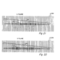
- Figures 21 and 22 show the actual results of a projectile test with the first described embodiment of the present invention.
- the set of data in Figure 21 shows a profile 250 of the tested projectile as viewed by the U plane sensor.
- Figure 22 shows a profile 252 of the same projectile as viewed by the V plane sensor.
- the horizontal axis in Figures 21 and 22 represents the line scan time (one line per microsecond) and the vertical axis represents a pixel location.
- Points 254 depict the projectile's shock wave in each plane, which can be measured simultaneously with other parameters of the tested projectile.
- the density of the shock wave pixels is proportional to the threshold settings at the time of firing of the projectile, and so can be made more or less visible as described.
- the speed of the projectile as measured by the invention was determined to be within one percent; pitch and yaw within one milliradian; and dispersion, i.e., locations of target impacts, within one-half millimeter.
- the invention was insensitive to environmental conditions normally encountered in the field as well as shock effects from repeated gun firings.
Abstract
Description
- The present invention relates to an electronic sensing apparatus according to the preamble of
claim claim 8. - Such an apparatus or method, respectively, is known from US-A-4 272 189. This known electro- optical projectile analyzer uses light beams from two perpendicular linear arrays of light emitters which impinge on corresponding linear photodetector arrays. After thresholding and digitizing, the received signals are fed to a processing means in order to evaluate certain parameters with respect to trajectory, shape of the projectile, etc.
- Furthermore, US-A-3 727 069 shows a system for measuring the location and diameter of a projectile in a frame of reference which includes vertical and horizontal banks of light sources for projecting collimated beams of light across the target area and corresponding vertical and horizontal banks of light receptors for indicating the location and diameter of a projectile passing through the target frame.
- Departing from the above-indicated prior art, it is the object of the present invention to devise a sensing apparatus and a method which allows for quick, automatic and simultaneous measurement of certain parameters as for e.g. speed, attack angle, shape, shock waves and dispersion of projectiles with said apparatus or method being suitable for automated scoring of data from projectiles fired at a high rate.
- This object is achieved according to the characterizing features of
claim - The present invention utilizes several light sensitive arrays which are illuminated by artificial or natural radiation, such as lasers or sunlight. The radiation is sensed in the form of several thin flat grids lying in parallel planes, each sensing radiation from different directions. The sensors are arrays of radiation-sensitive cells which are electronically interrogated at a high rate. The passage of projectiles between the light source and the arrays occludes the radiation to specific cells in accordance with the projectile profiles. These interruptions of sensed radiation by the cells are recorded and computed into parameters of the passing projectiles.
- One advantage of the present invention over the prior art is that it quickly, automatically and simultaneously measures speed, attack angle, shape, shock waves and dispersion of projectiles. The invention is suitable for either small or large projectiles, depending upon the embodiment of the invention utilized.
- Another advantage of the invention is that the cost per parameter is low. The measurements neither interfere with projectiles' flights nor require modifications to the projectiles. Large amounts of reliable and accurate data may be obtained over the whole projectile trajectories. The invention requires little dependence on externally supplied data. Still another object of the invention is that data reduction and turn-around time is fast making the invention suitable for automated "scoring" systems for taking data on a large series of projectiles fired at a high rate. The output of the invention is in a digital data format for easy transfer to computers for data reduction and analysis. Also, the invention is self-triggering upon the firing of the projectile and the projectile's entry into the sensing area of the invention.
-
- Figure 1 shows a sensing screen through which projectiles pass.
- Figure 2 is a block diagram of the electronics.
- Figure 3 is a schematic of an amplification and detection circuit.
- Figure 4 is a schematic of a fast trigger logic circuit.
- Figure 5 is a schematic of a logic circuit which combines the fast trigger logic outputs of the two planes.
- Figure 6 is a schematic of another fast trigger logic circuit.
- Figure 7 is a schematic of one of four identical circuits which together form the data acquisition system.
- Figure 8 shows the logic of a timing circuit.
- Figure 9 is a printout of processed data of a simulated small projectile test.
- Figure 10 shows a sequence of events for obtaining data in a projectile test.
- Figure 11 shows a sequence of events for analyzing data of a projectile test.
- Figure 12 shows another embodiment of the present invention.
- Figure 13 shows an optics and detector assembly.
- Figure 14 shows a sensing screen of a second embodiment of the present invention.
- Figure 15 is a block diagram of the analog electronics of a detector assembly.
- Figure 16 is a block diagram of another data acquisition system.
- Figure 17 shows the logic of timing and control of the other data acquisition system.
- Figure 18 shows another fast trigger logic configuration.
- Figure 19 is a printout of processed data of a simulated large projectile test.
- Figure 20 shows a detector assembly having fiber optics.
- Figures 21 and 22 show results of an actual projectile test from different planar views, respectively.
- Figure 1 shows an embodiment of an
electronic sensing screen 10 for detecting and taking data on projectiles which enter an active area plane 44, perpendicular to the plane 44.Lasers Lasers reflective mirrors optics reflective mirrors cylindrical lens Reflective mirrors - Each large cylindrical lens, 40 and 42, is about 20,3 cm (8 inches) wide and about 2,54 cm (1 inch) thick.
Lens light Laser beam planes Laser beam planes Laser beam planes photodiode arrays - In operation, a projectile enters through active area region 44 perpendicular to the
planes photodiode arrays arrays memory 56 of Figure 2, the contents of which provide an indication of the various parameters of the observed projectile. - At launch, an external start signal (IGN) is supplied to the electronic sensing screen. The observed time between launch and when the device is triggered (when it first detects the projectile passing through the chamber active area) is automatically saved. This allows the time between successive triggering of separate devices to be simply calculated. The fast trigger signal (TRIG) consists of a simultaneous "low" on two adjacent photocells on both planes. This criterion should be stringent enough to eliminate false triggering due to electrical transients. After gun launch, the device starts taking data and filling a temporary buffer which stores the last several microseconds of data. The number of microseconds of stored data is variable; for example it may be 1, 2, 4, 8, 16, etc., microseconds. After triggering, the data from this buffer, as well as all subsequent data, are stored in a high-speed memory. This continues until the memory is full. Afterwards, the "data ready" signal is sent to the external microcomputer to initiate data retrieval and start analysis.
- Figure 2 shows a block diagram of the invention. The outputs of
photodiode arrays threshold detection circuits specific circuits 47, one for each photodiode output, as illustrated in Figure 3. The output ofphotodiode 13 of photodiode array, 12 or 14, goes to the inverting input of anoperational amplifier 190. The noninverting input ofamplifier 190 is grounded. The feedback loop ofamplifier 190 has acapacitor 192 of about 5 picofarads and aresistor 194 which may be adjusted for the desired gain or amplification ofamplifier 190.Amplifier 190 may be an integrated circuit LM318. The output ofamplifier 190 goes to the inverting input of acomparator 196, which may be an integrated circuit MC3430. The noninverting input ofcomparator 196 is connected to a threshold reference voltage. When the voltage output level ofamplifier 190 crosses the value of the threshold reference voltage, then comparator 196 exhibits a signal which goes to an invertingbuffer 198. The output ofbuffer 198 goes tolatches fast trigger logic 60. - The outputs for each plane, U and V, viz., laser beam planes 43 and 45, from the amplification and
threshold detectors latches buffer 54 and go on to the first-in-first-out (FIFO)memory 56.FIFO 56 is a high-speed memory which may be an IDT 7M204-65 from Integrated Device Technology of Santa Clara, California. Data fromFIFO 56 are sent tocomputer 62 for data reduction and analysis. - Timing
block 58 provides a clock signal to latches 50 and 52,buffer 54 andFIFO 56.Fast trigger logic 60 receives inputs from amplification and threshold detectcircuits fast trigger logic 60 signal indicates light being blocked on any two adjacent photodiode cells inarrays fast trigger logic 60 goes toFIFO 56. These signals indicate that a projectile has entered active area 44 of Figure 1 and initiatestiming apparatus 58. The fast trigger logic signal causes data frombuffer 54 to be recorded intoFIFO 56.Buffer 54 andFIFO 56 may be incorporated as one unit. - Figure 4 shows an example of the
logic 61 of thefast trigger logic 60 for each plane. This example is for a 33-input plane. Onelogic 61 is utilized for the U plane and anotherlogic 61 is utilized for the V plane. Thefast trigger logic 60 receives its inputs from amplification andthreshold detection circuits logic 61 in Figure 4 is easily expandable to 128 or more photodiode outputs per plane. - In the operation of the
fast trigger logic 60, the inputs of ANDgates 64 are normally low. The normally low outputs of ANDgates 64 are input into a set of sixteen input ORgates 66. The normally low outputs of ORgates 66 are input into another sixteen-input ORgate 72. The normally low output ofOR gate 72 represents the output of thelogic 61 for either the U or the V plane. The AND/OR gates may utilize PAL 16C1 integrated circuits. - To obtain a
fast trigger logic 60 signal (TRIG), the light impinging the photodiodes must be obstructed from at least two adjacent photodiodes in each of the twoplanes threshold detection circuit gates 64 at the left oflogic 61 in Figure 4 will go high. If so, that means that at least one input ofOR gate 66 is high thus causing the normally low output of that ORgate 66 to go high. The high output ofgate 66 goes to anOR gate 72 causing the latter output to become high. - In order to double the number of inputs of
logic 61, one can take two of theselogic 61 circuits and connect their respective outputs to another OR gate. This process may be repeated as many times as needed to attain a sufficient number of inputs desired forlogic 61. - Figure 5 is the end-part of the
fast trigger logic 60 which combines thelogic circuit 61 outputs for planes U and V. A two-input ANDgate 74 receives the output from theU plane logic 61 and the output from theV plane logic 61. Both inputs to ANDgate 74 are normally low and thegate 74 output is normally low. Both the output oflogic 61 for the U plane and the output oflogic 61 for the V plane must be high for the output of ANDgate 74 to go high. The high output ofgate 74 indicates that light has been blocked to at least two adjacent photodiodes in the U plane and two adjacent photodiodes in the V plane. - The output of AND
gate 74 goes to the clock input offlip-flop 76, indicating that a projectile has entered the active area 44 of theelectronic sensing screen 10. The clear input to flip-flop 76 is the ignition (IGN) signal indicating that the projectile has been fired. Trigger outputs of flip-flop 76 indicate the projectile has been fired and that the projectile has entered the active area 44. -
Logic 61 may be designed in a variety of ways suitable to the desires of the designer or user. The number of photodiodes required to be blocked in either plane may be other than two. Also, thelogic 61 may be designed so as not to require a signal from both planes top indicate presence of a projectile of in the active area 44. - The present invention is not restricted to a
particular logic 61. For example, Figure 6 shows an alternative to the circuitry of Figure 4 for thelogic 61 of thefast trigger logic 60. Thelogic 61 in Figure 4 is different from thelogic 61 in Figure 6 in that the former accommodates 33 inputs, whereas thelogic 61 in Figure 6 accommodates 128 inputs utilizes differentintegrated circuits 78. The basic logic schematic of theseintegrated circuits 78 in Figure 6 may be essentially the same as that in Figure 4. Any other workable logic scheme is appropriate. Signals from the amplification andthreshold detection circuits trigger logic circuitry 61 of Figure 6, similarly as that of Figure 4. For instance, the outputs of amplification andthreshold detection circuit 46 are input into thecircuitry 61 of Figure 6 for the U plane and the outputs of amplification andthreshold detection circuit 48 are input into thecircuitry 61 of Figure 6 for the V plane. -
Integrated circuits 78 are programmable array logic integrated circuits type PAL 16C1. The PAL 16C1 is an AND gate array having inputs into an OR gate. Thisprogrammable array circuit 78 may be configured for the desired AND/OR connections reflecting various kinds of logic, including that of Figure 4. The outputs ofintegrated circuits 78 are input into an eight-input OR gate integratedcircuit 80. The output ofOR gate 80 is input into a two-input ORgate 82. The other input ofOR gate 82 is for accommodating a ninth programmable array logic integratedcircuit 78 which allows thecircuit 61 to accept 128 inputs from one of the amplification and threshold detection circuits, 46 or 48. The output ofOR gate 82 is equivalent to the output ofOR gate 72 in Figure 4. The circuitry of Figure 6 is an alternative to the circuitry of Figure 4. The output oflogic 61 of Figure 6 for each plane, U and V, is input into ANDgate 74 of Figure 5. - Figure 7 is a schematic of one of the four
circuits 55 which together form thedata acquisition system 59. Eachcircuit 55 is identical so that only one will be discussed in detail. Outputs of the amplification andthreshold detection circuits circuits 55. The firstsuch circuit 55 is connected to the odd photodiode signal outputs as conditioned by the amplification andthreshold detection circuit 46 for the U plane. Thesecond circuit 55 has its inputs connected to the even photodiode outputs as conditioned by the amplification andthreshold detection circuit 46 for the U plane. The thirdsuch circuit 55 has its inputs connected to the odd photodiode outputs as conditioned by the amplification andthreshold detection circuit 48 for the V plane. Thefourth circuit 55 has its inputs connected to the even photodiode outputs as the conditioned by the amplification andthreshold detection circuit 48 for the V plane. - The conditioned photodiode signals initially enter into
latches 84 of thedata acquisition system 59circuits 55 in Figure 7. There are 16latches 84 in the latches block 50 of Figure 2 for the U plane and 16latches 84 in latches block 52 of Figure 2 for the V plane. - In
circuit 55 of Figure 7, the signals in each of the eight latches 84, are taken out separately, upon receipt of a high signal fromdemultiplexer 88.Demultiplexer 88 sequentially takes data from each of the eight latches 84 and inputs it into the 4K-byte FIFO 86 at a rate of 8 MHz, i.e., approximately 125 nanoseconds perlatch 84. Thedemultiplexer 88 is cycled bycounter 90, which receives an 8 MHz clock signal. After the eight latches 84 are cycled through and data are taken from them, then the latches are simultaneously enabled to receive another set of data from the amplification andthreshold detection circuits latches 84 intoFIFO 86 and so on. Thelatches 84 are sequentially written to theFIFO 86 with the read line (R) set high (disabled) until an amount of data equal to the pretrigger setting (determined in support electronics 102) has been accumulated, whereupon the read line (R) and write line (WR) are simultaneously toggled. In this manner theFIFO 86 always retains a small queue containing the most recent data. The projectile is sensed, the FTL signal forces thesupport electronics 102 to hold the read line (R) high (disabled), the write line (WR) is not affected. Data is then written to theFIFO 86 until filled, whereupon the full flag (FF) signal generated byFIFO 86 simultaneously togglesmultiplexer 87 and sends a signal tocomputer 62 indicating data is ready to send. After the full flag (FF) is received bymultiplexer 87, the write (WR) line is held high (disabled) and the line which controlsFIFO 86 read pin is switched from read (R) to computer read (CR). After a full flag (FF) signal goes to thecomputer 62, thenFIFO 86 receives from thecomputer 62 an output enable (OE) signal and a computer read (CR) signal which toggles the data out of theFIFO 86 throughbuffer 92 out along data lines to the computer. Read (R) and write (WR) signals originate attiming circuit 58 of Figure 2. - Figure 8 shows the
timing circuit 58.Clock 94 runs at 8 MHz and is the basis for the timing of theelectronic sensing screen 10 system. The clock may be designed to operate at other frequencies, such as a lower one for testing slower projectiles. One output ofclock 94 goes to a divide-by-eightcounter 96, which in turn, outputs a 1 MHz clock signal to six four-bit timers 98. The four-bit timers 98 are connected in series and count increments of time from ignition (IGN) i.e., when a projectile is fired, to the time when theelectronic screen device 10 sees something in its active field of view 44. Timing signals from each of the three sets of four-bit timers go intobuffers 100. The outputs ofbuffers 100 are tied in to a set of data lines which go the computer. These data lines are common to the data lines from the fourcircuits 55 of Figure 7 fordata acquisition system 59. The computer does a selection with output enable signals (OE1, OE2 and OE3) when it desires data from one of the three timingbuffers 100 in Figure 8. When the computer wants to select data on the data lines from one of the fourcircuits 55 as represented by Figure 7, it will do so by toggling one of the output enable signals (OE) in Figure 7 for one of the respective fourcircuits 55 of thedata acquisition system 59. Only one of the output enable lines is toggled at a time for data. Each enable output line is sequentially toggled so that the computer can get all sets of data separately. When data is received down the data lines from one of the threebuffers 100 or from one of the fourdata acquisition circuits 55, all of the other sets of data lines outputs go to a state of high impedance.Support electronics 102 in Figure 8 provide read (R), write (WR) and clock (CLK) signals to thedata acquisition circuits 55. - Figure 9 shows a representative graphic display of processed data from the electronic
sensing screen device 10 for a tested projectile. Adisplay 11 shows a particular projectile recognizable by its profile as it passed through one of the planes. For the same projectile,display 11 can show another profile of the projectile in a plane orthogonal to the first plane. Also, angle of attack can be deciphered from these profiles. - Speeds of projectiles of interest might run up to 3000 m/s (10,000 feet per sec.) or 3 millimeters per microsecond. Thus, the photocell response and sampling rate must be high enough to ensure data-taking capability during the short time that the projectile is in the chamber active area 44. This is achieved at a sampling rate of 1 MHz. At this rate, a five inch projectile travelling at 3000 m/s (10,000 feet per second) will generate 42 "time slices" of data. Such a data rate exceeds the capability of most microcomputers. Thus, the data obtained are temporarily stored in small amount of fast memory resident in the
electronic sensing screen 10. The data are transferred to the microcomputer for analysis after the event. - A sequence of events of the
electronic sensing screen 10 apparatus is shown in a flow diagram in Figure 10. That flow diagram begins with "system power applied" and ends with a "memory full". Figure 11 is a flow diagram that is a continuation of the flow diagram in Figure 10. However, the flow diagram of Figure 11 shows the sequence of events after the data leaves the memory of theelectronic sensing screen 10, i.e., events outside theelectronic sensing screen 10 apparatus. The flow diagram in Figure 11 notes the processing steps of data after transfer from the memory of theelectronic sensing screen 10 apparatus. - The steps of the invention as shown by Figure 10 begin with applying power to the system and lasers, in that order. The system logic continually asks itself the question whether a projectile has been fired for test, until the answer to the question is yes. At the latter point, the timer is started. Then a photodiode data segment is latched and stored into the FIFO memory. The ensuing question is whether there is a preset amount of data segments stored. If not, another photodiode data segment is latched. If so, then the question is whether a trigger occurred. If not, then the oldest photodiode data segment is discarded and another photodiode segment is latched and stored in the FIFO memory. If a trigger has occurred, then the timer is stopped. Next, another photodiode data segment is latched and stored in the FIFO memory. The oldest data .segment is stored in the memory. After such memory storage, the question is whether the memory is full. If not, another photodiode segment is latched. This memory question continues to be asked until the memory is full.
- Figure 11 shows the steps of the test when the memory is deemed full as indicated at the bottom of Figure 10. A full memory of data is transferred into a computer. The computer determines the location of the projectile image in the data field and then makes an initial guess for state parameters. That guess of those parameters is used to portray a cross-section image of a three-dimensional model of the tested projectile. The model is stored in the computer's memory. Next, the model image is compared with the data image via a "least squares" fit or another mathematical comparison method. After such comparison there is the question whether the fit of the comparison has converged. If the answer is no, then the latest guess for state parameters is used to update the cross-section image of the three-dimensional model of the projectile in the computer memory. The model image is compared to the data image via the "least squares" fit or other mathematical comparison method and then the question whether the fit has converged, is reasked. If the answer is yes, then the state parameters and fit results are displayed. That display is the end of the data analysis.
- The above described
embodiment 10 is suitable for measuring small caliber projectiles. Small caliber projectiles are fast and may be contained to small areas for measurement. Large caliber projectiles, on the other hand, are slower and require a larger area for operational testing. Thus, a practicable place for measuring large projectiles is outdoors utilizing natural radiation from the sky. The latter is achieved by anembodiment 104 of Figure 12 as described below. - The major components of
embodiment 104 for large active areas major components for systems blocks include: an optical anddetector assembly 106; the data acquisition electronics; and the fast trigger logic. Various modifications to the basic components can be made to enhance a particular feature such as resolution, cost, or complexity. However, the basic function and logic of the data acquisition electronics will not change any of the basic functions described herein, except perhaps as to the specifics of interfacing the data acquisition electronics to the detector system selected. Similarly, the optical assembly must fulfil certain basic functions for successful device operation, but specific details such as how to interface the optics to the detector depend on the detector choice and may entail minor modifications to the optics to account for detector size, intensity requirements, etc. Thus, the choice of detector assembly will most affect device operation and its applicability to specific projectile test scenarios. Three types of detector concepts are presented here, each having different characteristics which may make one concept preferable to a particular kind of testing. - The CCD concept is one of the cheapest and easiest detector concepts to implement. A high speed CCD line scanning photodiode array such as the CCPD RL1288D by EG&G has the speed and sensitivity under adequate light conditions. However, under low light conditions, the photodiode array's integration time may have to be extended to assure sufficient accumulation of light. If this integration time becomes too long then insufficient data on the projectile will be obtained by the time the projectile leaves the active area. In some configurations, image intensifiers may solve this problem.
- Another photodiode concept is a direct extension of the small earlier design. Light from the optical assembly is focused on a custom built photocell array and each cell is individually coupled to amplification and threshold detection electronics. The outputs of the threshold detection circuit are directly fed to fast trigger logic and the data acquisition electronics whose architecture is the same as the first embodiment described.
- A fiber optics concept uses optical fibers to couple light from a screen upon which a projectile image is focused, to individual PIN photodiodes. The photodiode outputs can be coupled to very sensitive amplifiers to achieve low light sensing characteristics for the electronic sensing screen system.
-
Embodiment 104 for measuring large caliber projectiles may utilize the same electronics as described above in theembodiment 10 for measuring small caliber projectiles. However, an alternative set of electronics is described here forembodiment 104. - Figures 12 through 19 illustrate
embodiment 104 of the invention. The optics anddetector 106 sense natural radiation, such as from the sun, and any occlusion of that radiation by a projectile is detected by optics anddetector assembly 106 and transferred electronically to the electronics ofembodiment 104. The optics anddetector 106 can be elevated at angle A, as desired relative to the horizontal, for looking at a projectile. - Figure 13 shows an example of the optics and
detector assembly 106 used to cover a field of view and to focus the light of the view on aphotocell detector 118.Lenses optical assembly 106 is about 1 centimeter wide and extends indefinitely at that width. The field of view from the side view varies with an adjustable openingangle B. Lenses Lenses pin hole aperture 114 onto thephotocell array 118. The optics anddetector assembly 106 may be modified with additional, less or different optics. Also, filters may be used as desired. Theoptics 106 compose a high quality assembly which is corrected for as many aberrations as possible to achieve optimum focus at thepinhole aperture 114. This high quality correction is necessary for the collimation properties of the optical assembly to be as high as practicable. - Photocell (CCD)
array 118 may be a model number RL1288D, available from EG&E Reticon of Sunnyvale, California. This photocell array and its built-in associated electronics are described in the manufacturer's specifications on the RL1288D. The associated electronics may include shift registers, capacitors, sample-and holds, gates, etc. The array is an ultra-high speed, soft-scan, charge-coupled, linear photodiode array with video output taps for every 128 diodes. This array has eight sections with 1024 diode resolution. It has a wide spectral response from near ultraviolet to near infrared. Each block of 128 pixels has two shift registers for readout, one for odd numbered pixels within a section (odd video channel) and the other for even numbered pixels within a section (even video channel). Thus,photodiode array 118 has sixteen CCD analog shift registers and the same number of video output lines. - Light incident on the sensing aperture of
array 118 generates photocurrent which is integrated and stored as a charge on the capacitance of each of the photodiodes. At the end of each integration period, the charges on all of the diodes are simultaneously switched through transfer gates into CCD analog shift registers for readout. Immediately after this parallel transfer, a new integration period begins. The integration periods and charge or signal transfers are controlled by clock signals from a 100 KHzintegration clock 124 and an 8 MHzshift register clock 122 in Figure 15. - Figure 14 shows the spatial position of the
electronic sensing screen 104 optics anddetector 106 set-ups relative to theactive area 105 through which a projectile passes for parameter measurement. Figure 14 shows the shape of the field of view of twodetector 106 systems, which is the preferred arrangement. The overlap of the two fields of view constitutesactive area 105, similar to the active area 44 of Figure 1. Use of only oneelectronic sensing screen 104 allows measurements of the speed, dispersion and the orientation of the projectile in the plane perpendicular to the optical axes. The error in the dispersion would thus be greater because the distance of the projectile from the optics would have to be estimated from the projectiles' apparent magnification on the output data as displayed in Figure 19. The fan-like shape of the field of view means that the measurement resolution depends upon the opening angle B chosen and the distance between the projectile and the optics. If, for a fixed opening angle B, a projectile is brought closer to the optics, the finer resolution is at the expense of a smalleractive area 105. As an example of the resolution expected from the device, adjusting the field of view to create a 116,7 m2 (1256 square foot) active area (i.e., a 12,16 m diameter circle) achieves an average cell size of less than 1,6 cm2 (.25 square inches). - The optical opening angle B, may be adjusted between 5-10° and the detector elevation angle A can be adjusted as desired. This latitude makes it easy to accommodate a large number of active area and target height combinations. An active area may vary from the equivalent of a 12,16 m (40 foot) diameter circle, 91,2 m (300 feet) off the ground to a 1,06 (3.5 foot) diameter circle, 6,08 m (20 feet) off the ground. However, ultimately, the distance between the optics and the projectile (slant-range) is limited by the collimation properties of
optics 106. - Figure 15 is a functional block diagram of the analog electronics. The optics and
detector assembly 106 in Figure 15, is described in the above discussion of Figure 13. A 100 KHzintegration clock 124 initiated by the ignition (IGN) signal, determines integration time, i.e., photodiode cell exposure time. When light strikes a photodiode cell, the cell discharges a capacitor which is pre-charged to a certain level. Every 10 microseconds the contents of the capacitor pertaining to the respective photodiode cell are dumped into an analog shift register via a sample-and-hold type circuit which transfers the contents or samples the contents. - This system may be used on either cloudy or sunny days. However, on some cloudy days, longer integration times may be necessary if the ambient light levels are not sufficiently high enough to saturate the photodiode cells before the integration time is expended. With longer integration times, the data dump from each photocell would be more infrequent and thus the system slower which may be yet satisfactory for slow moving projectiles. If the times of integration are not sufficient then not all photodiodes will saturate thus resulting in a signal indicating a shade rather than "black or white". The presently described embodiment may functionally provide discrete "black or white" indications or indications of various shades of grey.
- The data from the 1024 photodiode cell capacitors are simultaneously put into 16 analog shift registers. The 16 shift registers' data are serially and simultaneously clocked out by an 8
MHz clock 122.Clock 122 is enabled byclock 124.Clock 122 allows the whole array to be read in 8 microseconds. The data are fed into 16 four-bit analog-to-digital converters 126 in Figure 15. For each bit of information from a photodiode cell analog shift register, an analog-to-digital converter 126 creates a four-bit word. This improvi- sion is in place to accommodate various shades of information from each photodiode as desired. Output of the analog-to-digital converter 126 may be either a four-bit word of all zeros, a four-bit word of all ones or a mixture of ones and zeros for various shades. The four-bit words from the sixteen analog-to-digital converters 126 go into aninternal data bus 128 of 64 bits, i.e., 16 four-bit words in parallel. From the analog-to-digital converters 126, the data, via theinternal data bus 128, go on to the data acquisition system t30 of Figure 16, and to thefast trigger logic 132 of Figure 18. - Figure 16 shows the block diagram of the
data acquisition electronics 130. The data from theinternal data bus 128 is read by a first-in-first-out (FIFO)buffer 134 to allow up to 150 microseconds of pretrigger data. When the projectile is sensed by the fast trigger logic (FTL) 132, the data is allowed to fill theRAM 136. After theRAM 136 is full, thecontrol logic 140 halts data taking, opens the external data bus viabuffers 138, and writes the data to a parallel-to-serial shift register 142 for transmission to an external computer. - The output data, from analog-to-
digital converters 126 of Figure 15, along theinternal data base 128 are fed into the pre-trigger FIFO's 134 of Figure 16 in the form of eight-bit words, i.e., four-bit words from two analog-to-digital converters 126, which are combined for eachFIFO 134 input. FIFO's 134 hold 1024 x 9 bits and may be obtained from Integrated Device Technology of Santa Clara, California. Data from theinternal data base 128 can be fed into FIFO's 134 continuously without the data going anywhere else. However, when FIFO's 134 receive a fast trigger logic signal, then the FIFO's 134 dump their existing data into corresponding 8 K-bit RAM's 136. After the RAM's 136 are full, they stop taking data. One full line scan of data takes up 64 eight-bit bytes in either the pre-trigger FIFO's 134 or the RAM's 136. FIFO's 134 can take up to a maximum of sixteen line scans of data as a pretrigger period before they are full. Yet, since the fast trigger logic signal is asynchronous, they may hold fewer than sixteen line scans when the fast trigger logic signal, i.e., entry of projectile intoelectronic sensing screen 104active area 105, indicates transfer of data into the RAM's 136. Therefore, data entry into RAM's 136 has to be held off until a new line scan is started in control andtiming logic 140. The RAM's 136 can hold up to 128 line scans. After the RAM's 136 are full, the data can be read out and sent on to a computer or microcomputer. - The input ports of each of the RAM's 136 are also the output ports of the RAM's 136. Thus, when data are being taken out of RAM's 136, no data are being transferred into the RAM's 136. As data are being transferred out, the data go through
buffers 138 onto the parallel-to-serial shift register 142 which takes the data and puts it into a strict serial format. This procedure of using the same port for both inputting and outputting data may be avoided with dual port RAM's. - The data from the parallel-to-
serial shift register 142 are sent out to a microcomputer for data reduction and analysis. When data are to be taken out of RAM's 136,address generator 139 andbuffers 138 receive signals to effect that transfer. The data from the RAM's 136 are sequenced out from oneRAM 136 at a time, beginning from right to left in Figure 16. For instance, on the far right, whenRAM 136 has transferred all of its data through the far-right buffer 138 into the parallel-to-serial shift register 142, then data are taken out of the second from theright RAM 136 and are transferred through the second from theright buffer 138 and through the far-right buffer out onto the parallel-to-serial shift register 142, and so on, until one gets to the far-leftRAM 136, data are transferred out of thatRAM 136 through all thebuffers 138 to the parallel-to-serial shift register 142. The reason for putting the data into strict serial format byshift register 142 is that this data may be transferred a great distance with more reliability than parallel transmission of such data. However, parallel transmission may be utilized for quicker transfer of data. - The
address generator 139 consists of counters which count from 0 to 8 K, or so, for reading data from all of the FIFO's 134 into all of the RAM's 136, simultaneously. Theaddress generator 139 also cycles the memory for reading out data out of each of the RAM's 136. However, in reading out, the RAM's 136 are addressed only one at a time. An 8MHz clock 144, which is a basis for timing in thedata acquisition system 130, feeds the clock signal into the control andtiming logic 140 which passes on the 8 MHz clock signal to the address generator. When data are being read into RAM's 136, all thebuffers 138 are off. - The timing and
control logic 140 of Figures 16 and 17 has three basic functions: control of the FIFO's 134 read/write (R/W) function, control of the RAM's 136 R/W function, and control of the computer interface sequence. Each of these functions is initiated and kept in sequence by four control lines: the fast trigger logic (TRIG) pulse, the external projectile fire (IGN) pulse, the start line scan (SLS) pulse, and the 8 MHz clock (CLK) pulses. - The
FIFO control block 202 generates aFIFO 134 read enable and toggles the R/W line at the internal data rate immediately upon receiving an IGN pulse. Data are taken until the pretrigger is satisfied, whereupon theFIFO 134 write enable is generated. Simultaneous reads and writes continue until aRAM 136 full signal is obtained. After theRAM 136 full is sensed, data taking is stopped. - The
RAM control block 204 generates aRAM 136 read enable after receiving a simultaneous fast trigger logic (TRIG) signal and a start line scan (SLS) signal through ANDgate 200, thus ensuring that no partial line scan data are taken. TheRAM control block 204 is responsible for toggling the R/W line and address line appropriately during data taking. ARAM 136 full signal stops data taking, signals the external computer to start reading data, and transfers control to acomputer control block 206. - The
computer control block 206 is an interface with a computer or microcomputer. Thecomputer control block 206 is initiated after aRAM 136 full signal is received.Block 206 is responsible for keeping the two-byte buffer in the parallel-to-serial shift register 142 filled with data to be sent to the external computer. To this end, theblock 206 sequentially reads each RAM 136 (after enabling theappropriate buffers 138 used to isolate the eight separate RAM 136 -FIFO 134 data buses) and writes this data to the parallel-to-serial shift register 142. Hand-shaking with the external computer is controlled by the parallel-to-serial shift register 142. - Figure 18 shows a block diagram of a
fast trigger logic 132 electronics. During the first 10 microsecond data cycle after the fire pulse is received (the IGN pulse), a digital value of each cell's charge storage (which is the measure of the light intensity reaching that cell), minus a preselected threshold, is stored in a small amount of memory. On each subsequent data cycle, the current cell intensity is compared to the stored threshold value and flagged if smaller. When the number of cells with the smaller intensity exceeds another preselected value, the trigger is satisfied. In this way, thefast trigger logic 132 in Figure 18 is somewhat like an automatic gain control for ambient light conditions of theelectronic sensing screen 104 apparatus. It measures the light conditions to determine if there is any change in them from one projectile firing to another. Constant light conditions are assumed during each projectile's travel time. -
Fast trigger logic 132 obtains light intensity data from theinternal data bus 128. The first line scan ofphotodiode array 118 of theelectronic sensing screen 104 is used to determine the ambient light conditions. Four bits of data on existing light conditions come intoadder 154 fromdata bus 128. To this value of four bits,adder 154 adds a certain pre-set value, such as a binary 1 or 2, from a four-bit switch 148 to each four-bit byte and stores the result in astatic RAM 156. The four-bit switch 148 is a threshold preselect binary switch. Thus, the modified line scan is stored in thestatic RAM 156 with a slightly enhanced value of the ambient light conditions. That value of the light conditions is compared by acomparator 158 with another first line scan when the next projectile is fired. This procedure of evaluating merely the first line scan of a projectile firing, is made under the assumption, which is very likely, that by the time the projectile reaches theactive area 105 from the moment it starts at the firing time, the ambient light conditions are likely to remain the same. However, since from one shot to the next shot there may be a change in the ambient light conditions, these conditions are checked every time a new projectile is fired. - The
fast trigger logic 132 may be described in another manner.Address generator 150 of Figure 18 generates an address for thestatic RAM 156, which is done once at the beginning of an ambient light check. On the next line scan, information comes in directly to thecomparator 158 which compares the new value with the value in thestatic RAM 156 in terms of four binary bits. If the new value is lower, then thecomparator 158 sets counter 160 and counts the number of cells that are lower than the "set value". What actually is happening is that the old data, i.e., the first line scan, are compared to the new data, i.e., the next line scan, and then thecounter 160 just counts the number of cells that are lower and compares this counter value with another preset value from four-bit switch 152, which indicates the number of cells needed to be low, i.e., whatever value is selected, for presenting a fast trigger logic signal to ORgate 164. - Each of the two
preselect switches switch 148 is the threshold switch for adding a certain value to the initial state of light conditions. Theother preselect switch 152 tells how many pixels have to be lower than threshold level, or what number of cells have to be low, in order to create a fast trigger logic signal to be sent to ORgate 164. - Overall, in the fast
trigger logic circuit 132 of Figure 18, there are 16 comparator-type circuits 146 which includeadder 154,static RAM 156,comparator 158, counter 160 andcomparator 162. The outputs of thecircuits 146, i.e., coming out of thecomparator 162, go into ORgate 164. When there is a signal from any of thesecircuits 146, ORgate 164 sends out a fast trigger logic signal (TRIG) which indicates that the projectile has entered theelectronic sensing screen 104active area 105.Circuit 166 in Figure 18 consists of thethreshold preselect switch 148, thepreselect switch 152, and theaddress generator 150. There is only onecircuit 166 and it is connected, in common, to all 16circuits 146. - Figure 19 shows a printout of the data in graphic form of a projectile having passed through the
electronic sensing screen 104active area 105. After the extraction of the data from the invention, the data are then analyzed by a computer. Figure 19 shows an example of how part of the raw data might appear for a projectile with a tail boom and fins. For the purpose of this example, the projectile is assumed to be 1,01 m (40 inches) long, travelling at 1976 m/s (6560 feet per second) with a 1° pitch angle and passing through the center of an active area defined by a 12,16 m (40 foot) diameter circle. The cells which were obscured by the projectile passage appear as ""asterisks"" while the unobscured are "ones". This type of data pattern is called a "profile pattern". Another type of data pattern may provide shade information resulting in a photographic representation of the projectile. The velocity of the projectile can be obtained from one or both of two methods - directly from the profile pattern if the projectile length is known or, alternatively, via a "time of flight" determination between the two successive sensing grids. - Other parameters are obtainable. Dispersion is determined from a sequence of profiles for a series of projectile firings. Values of pitch and yaw can be computed from the profile "centers" at different positions along the shell, i.e., different times of data taking. However, all of the parameters are better determined with a computer which can fit the profile pattern to a model of the projectile shape stored in memory, and adjusting the parameters until the best fit is obtained. Such shape and profile fitting and comparison methods result in substantial improvement in accuracy. The computer can also correct the data for distortions due to projectile distance from the detector, optical opening angle and any known optical aberrations in the field of view.
- A third embodiment is similar to the second embodiment, by utilizing two
electronic sensing screens 104 composingactive area 105 within which projectile parameters are measured. The third embodiment is similar to the first embodiment by utilizing the same electronics. The unique feature of the third embodiment is the detector assembly as shown in Figure 20. It utilizes a fiber optics bundle 172 to convey image data from theoptics 174 toPIN photodiode 176. Fiber ends 178, upon which an image is focused, are next to each other in a collinear fashion. The fibers may be as small as 125 microns, so that 1000 strands can form a flat cable of only 12.5 cm wide. The other flat ends 180 of thefiber 182 of thefiber optics cable 172, are each coupled to aPIN photodiode 176. The output of eachphotodiode 180 goes to the amplification andthreshold detection circuit fiber 180 can be made as sensitive as necessary to achieve the necessary data-sensing characteristics. - This embodiment avoids the problems of the second embodiment in situations where environmental light conditions impose unacceptable long integration time requirements on the
CCD detector array 118 of Figure 15, by allowing essentially instantaneous transfer of data regarding the light level at any point in the field of view illustrated in Figure 14. The third embodiment avoids the requirements of special light sources of the first embodiment by avoiding the problems of noise and "cross-talk" of adjacent photodiodes needing to be sensitive to low intensity light variations under natural ambient light conditions of the environment. - Figures 21 and 22 show the actual results of a projectile test with the first described embodiment of the present invention. The set of data in Figure 21 shows a
profile 250 of the tested projectile as viewed by the U plane sensor. Figure 22 shows aprofile 252 of the same projectile as viewed by the V plane sensor. The horizontal axis in Figures 21 and 22 represents the line scan time (one line per microsecond) and the vertical axis represents a pixel location. -
Points 254 depict the projectile's shock wave in each plane, which can be measured simultaneously with other parameters of the tested projectile. The density of the shock wave pixels is proportional to the threshold settings at the time of firing of the projectile, and so can be made more or less visible as described. - All the projectile parameters that the invention was designed to measure were actually measured to the predicted high precision. The results were compared with other measurement methods, excluding the present invention, within estimated errors. The speed of the projectile as measured by the invention was determined to be within one percent; pitch and yaw within one milliradian; and dispersion, i.e., locations of target impacts, within one-half millimeter.
- Excellent reliability of the invention was demonstrated by the testing. The invention was insensitive to environmental conditions normally encountered in the field as well as shock effects from repeated gun firings.
Claims (9)
Applications Claiming Priority (2)
| Application Number | Priority Date | Filing Date | Title |
|---|---|---|---|
| US31951 | 1979-04-20 | ||
| US07/031,951 US4864515A (en) | 1987-03-30 | 1987-03-30 | Electronic sensing screen for measuring projectile parameters |
Publications (2)
| Publication Number | Publication Date |
|---|---|
| EP0342201A1 EP0342201A1 (en) | 1989-11-23 |
| EP0342201B1 true EP0342201B1 (en) | 1991-01-23 |
Family
ID=21862274
Family Applications (1)
| Application Number | Title | Priority Date | Filing Date |
|---|---|---|---|
| EP88902282A Expired EP0342201B1 (en) | 1987-03-30 | 1988-02-05 | Electronic sensing apparatus for measuring projectile parameters |
Country Status (3)
| Country | Link |
|---|---|
| US (1) | US4864515A (en) |
| EP (1) | EP0342201B1 (en) |
| WO (1) | WO1988007685A1 (en) |
Families Citing this family (40)
| Publication number | Priority date | Publication date | Assignee | Title |
|---|---|---|---|---|
| US5005147A (en) * | 1988-12-30 | 1991-04-02 | The United States Of America As Represented By The Administrator, The National Aeronautics And Space Administration | Method and apparatus for sensor fusion |
| US5107103A (en) * | 1990-01-26 | 1992-04-21 | Carnegie-Mellon University | Integrated circuit having at least a sensor and a processor thereon |
| IT1256286B (en) * | 1991-08-21 | 1995-11-29 | Alenia Aeritalia & Selenia | PRE-PROCESSOR FOR THE DETECTION OF POINT SOURCES IN SCENARIOS IN THE INFRARED. |
| US5311271A (en) * | 1992-01-21 | 1994-05-10 | Dme/Golf, Inc. | Golf course range finder |
| US5369284A (en) * | 1993-03-30 | 1994-11-29 | The Charles Stark Draper Laboratory, Inc. | Active edge position measuring device |
| US5297061A (en) * | 1993-05-19 | 1994-03-22 | University Of Maryland | Three dimensional pointing device monitored by computer vision |
| US5491642A (en) * | 1993-12-03 | 1996-02-13 | United Technologies Corporation | CCD based particle image direction and zero velocity resolver |
| DE4416559A1 (en) * | 1994-05-11 | 1995-11-30 | Daimler Benz Aerospace Ag | Projectile speed and flight altitude-position determination unit for testing armour plating |
| US5512998A (en) * | 1994-06-22 | 1996-04-30 | The Titan Corporation | Contactless method and system for determining static and dynamic characteristics of target objects |
| US5701172A (en) * | 1995-06-07 | 1997-12-23 | Gas Research Institute | Optical flowmeter |
| US20040014010A1 (en) * | 1997-08-25 | 2004-01-22 | Swensen Frederick B. | Archery laser training system and method of simulating weapon operation |
| EP1007896B1 (en) * | 1997-08-25 | 2004-12-29 | Beamhit L.L.C. | Network-linked laser target firearm training system |
| US6777663B2 (en) * | 1999-05-07 | 2004-08-17 | Intel Corporation | Enhanced Photocell with sample and hold amplifier |
| JP2003519774A (en) * | 2000-01-13 | 2003-06-24 | ビームヒット,リミティド ライアビリティー カンパニー | Firearms laser training system and method utilizing an improved empty cartridge to simulate firearm operation |
| US6505140B1 (en) | 2000-01-18 | 2003-01-07 | Intelligent Automation, Inc. | Computerized system and method for bullet ballistic analysis |
| US6785634B2 (en) * | 2000-01-18 | 2004-08-31 | Intelligent Automation, Inc. | Computerized system and methods of ballistic analysis for gun identifiability and bullet-to-gun classifications |
| US6616452B2 (en) * | 2000-06-09 | 2003-09-09 | Beamhit, Llc | Firearm laser training system and method facilitating firearm training with various targets and visual feedback of simulated projectile impact locations |
| US6795068B1 (en) * | 2000-07-21 | 2004-09-21 | Sony Computer Entertainment Inc. | Prop input device and method for mapping an object from a two-dimensional camera image to a three-dimensional space for controlling action in a game program |
| US6628995B1 (en) * | 2000-08-11 | 2003-09-30 | General Electric Company | Method and system for variable flight data collection |
| US6563763B2 (en) * | 2001-04-03 | 2003-05-13 | Aai Corporation | Method and system for correcting for curvature in determining the trajectory of a projectile |
| EP1402224A2 (en) | 2001-06-08 | 2004-03-31 | Beamhit, LLC | Firearm laser training system and method facilitating firearm training for extended range targets with feedback of firearm control |
| JP4235729B2 (en) * | 2003-02-03 | 2009-03-11 | 国立大学法人静岡大学 | Distance image sensor |
| US8133115B2 (en) | 2003-10-22 | 2012-03-13 | Sony Computer Entertainment America Llc | System and method for recording and displaying a graphical path in a video game |
| CA2577969A1 (en) * | 2004-08-31 | 2006-03-09 | Intelligent Automation, Inc. | Automated system and method for tool mark analysis |
| US20060071933A1 (en) | 2004-10-06 | 2006-04-06 | Sony Computer Entertainment Inc. | Application binary interface for multi-pass shaders |
| IL167932A (en) * | 2005-04-10 | 2012-03-29 | Israel Aerospace Ind Ltd | Systems and methods for detecting the position of an object passing through optical screens |
| US7636126B2 (en) | 2005-06-22 | 2009-12-22 | Sony Computer Entertainment Inc. | Delay matching in audio/video systems |
| US7684020B1 (en) * | 2005-09-02 | 2010-03-23 | Artis, Llc | Sensor system and method for detecting and identifying rapidly moving objects |
| US20070202959A1 (en) * | 2006-01-23 | 2007-08-30 | Rankin David B | Imaging system and method including multiple, sequentially exposed image sensors |
| US7880746B2 (en) | 2006-05-04 | 2011-02-01 | Sony Computer Entertainment Inc. | Bandwidth management through lighting control of a user environment via a display device |
| US7965859B2 (en) | 2006-05-04 | 2011-06-21 | Sony Computer Entertainment Inc. | Lighting control of a user environment via a display device |
| US10786736B2 (en) | 2010-05-11 | 2020-09-29 | Sony Interactive Entertainment LLC | Placement of user information in a game space |
| DE102010036883A1 (en) * | 2010-08-06 | 2012-02-09 | Sick Ag | Optoelectronic sensor |
| US9342817B2 (en) | 2011-07-07 | 2016-05-17 | Sony Interactive Entertainment LLC | Auto-creating groups for sharing photos |
| US11933585B2 (en) | 2013-03-27 | 2024-03-19 | Nostromo Holdings, Llc | Method and apparatus for improving the aim of a weapon station, firing a point-detonating or an air-burst projectile |
| US10514234B2 (en) | 2013-03-27 | 2019-12-24 | Nostromo Holdings, Llc | Method and apparatus for improving the aim of a weapon station, firing a point-detonating or an air-burst projectile |
| US9600900B2 (en) | 2013-03-27 | 2017-03-21 | Nostromo Holdings, Llc | Systems to measure yaw, spin and muzzle velocity of projectiles, improve fire control fidelity, and reduce shot-to-shot dispersion in both conventional and air-bursting programmable projectiles |
| EP2784518A3 (en) * | 2013-03-27 | 2014-12-10 | KMS Consulting, LLC | Projectile and projectile flight parameter measurement apparatus for a weapon |
| CN106767911B (en) * | 2016-11-30 | 2020-03-10 | 中国航空工业集团公司沈阳飞机设计研究所 | Method and system for signal acquisition and fault monitoring of angle of attack sensor |
| US11442075B2 (en) * | 2019-01-23 | 2022-09-13 | Charles Hardy | Ballistic projectile velocity measurement apparatus |
Family Cites Families (14)
| Publication number | Priority date | Publication date | Assignee | Title |
|---|---|---|---|---|
| DE1272778B (en) * | 1965-11-17 | 1968-07-11 | Drello Ing Paul Drewell | Light barrier, especially for measuring the speed of flying bodies |
| US3727069A (en) * | 1971-07-21 | 1973-04-10 | Litton Systems Inc | Target measurement system for precise projectile location |
| US4097800A (en) * | 1977-01-12 | 1978-06-27 | The United States Of America As Represented By The Secretary Of The Army | Laser screen |
| US4185191A (en) * | 1978-06-05 | 1980-01-22 | Honeywell Inc. | Range determination system |
| US4230942A (en) * | 1979-03-26 | 1980-10-28 | Honeywell Inc. | Crossed cylindrical lens |
| US4289960A (en) * | 1979-07-03 | 1981-09-15 | The United States Of America As Represented By The Secretary Of The Army | Artillery training rounds target scoring system |
| US4272189A (en) * | 1979-08-16 | 1981-06-09 | The United States Of America As Represented By The Secretary Of The Navy | Electro-optical projectile analyzer |
| US4313109A (en) * | 1979-12-11 | 1982-01-26 | Sperry Corporation | Initialization control for light beam position indicator |
| US4317991A (en) * | 1980-03-12 | 1982-03-02 | Honeywell Inc. | Digital auto focus system utilizing a photodetector array |
| US4329060A (en) * | 1980-04-14 | 1982-05-11 | Sangamo Weston, Inc. | Non-contacting workpiece gauging system |
| US4425501A (en) * | 1981-03-30 | 1984-01-10 | Honeywell Inc. | Light aperture for a lenslet-photodetector array |
| US4410804A (en) * | 1981-07-13 | 1983-10-18 | Honeywell Inc. | Two dimensional image panel with range measurement capability |
| AT371938B (en) * | 1981-12-16 | 1983-08-10 | List Hans | DEVICE FOR SUPPRESSING INTERFERENCE SIGNALS IN BALLISTIC MEASUREMENTS WITH PHOTOCELLS |
| SE440150B (en) * | 1984-05-08 | 1985-07-15 | Stiftelsen Inst Mikrovags | DEVICE FOR OPTICAL SEATING OF THE MOVEMENT OF A FORMAL |
-
1987
- 1987-03-30 US US07/031,951 patent/US4864515A/en not_active Expired - Fee Related
-
1988
- 1988-02-05 WO PCT/US1988/000318 patent/WO1988007685A1/en active IP Right Grant
- 1988-02-05 EP EP88902282A patent/EP0342201B1/en not_active Expired
Also Published As
| Publication number | Publication date |
|---|---|
| WO1988007685A1 (en) | 1988-10-06 |
| EP0342201A1 (en) | 1989-11-23 |
| US4864515A (en) | 1989-09-05 |
Similar Documents
| Publication | Publication Date | Title |
|---|---|---|
| EP0342201B1 (en) | Electronic sensing apparatus for measuring projectile parameters | |
| CA1138092A (en) | Monitoring system for measuring kinematic data of golf balls | |
| US5298905A (en) | Visible light detection and ranging apparatus and method | |
| US6535275B2 (en) | High resolution 3-D imaging range finder | |
| US4601053A (en) | Automatic TV ranging system | |
| AU626157B2 (en) | Imaging lidar system using non-visible light | |
| US7710545B2 (en) | Scanned laser detection and ranging apparatus | |
| US5696577A (en) | 3D imaging underwater laser radar | |
| EP1147370B1 (en) | Self gating photosurface | |
| US4937445A (en) | Apparatus for determining the distances of points on a surface from a reference axis | |
| EP0022263B1 (en) | Light curtain apparatus with provision for generating a cyclically varying scale signal | |
| KR920704503A (en) | High resolution multi-sensor camera | |
| GB2037980A (en) | Measuring the shape of a glass gob | |
| US4993835A (en) | Apparatus for detecting three-dimensional configuration of object employing optical cutting method | |
| US4482252A (en) | Calibration method and apparatus for optical scanners | |
| US5221928A (en) | Method and apparatus for accurate, high speed pulse-echo measurement calibration | |
| US4119379A (en) | Optical detection and ranging apparatus | |
| EP0080353B1 (en) | Apparatus and method for measuring temperature profile | |
| AU610202B2 (en) | Device for selective detection of objects | |
| US5640240A (en) | Probe for surface measurement | |
| US4747574A (en) | Apparatus for acquisition of the surface shape of a distant object by means of picture element scanning | |
| GB1513380A (en) | Position indicating system | |
| US4553838A (en) | Optical inspection system | |
| US5017004A (en) | Multifunction electro-optical system test tool | |
| US6885448B2 (en) | Photon correlator |
Legal Events
| Date | Code | Title | Description |
|---|---|---|---|
| PUAI | Public reference made under article 153(3) epc to a published international application that has entered the european phase |
Free format text: ORIGINAL CODE: 0009012 |
|
| 17P | Request for examination filed |
Effective date: 19890829 |
|
| AK | Designated contracting states |
Kind code of ref document: A1 Designated state(s): CH DE FR GB LI NL |
|
| 17Q | First examination report despatched |
Effective date: 19900523 |
|
| GRAA | (expected) grant |
Free format text: ORIGINAL CODE: 0009210 |
|
| AK | Designated contracting states |
Kind code of ref document: B1 Designated state(s): CH DE FR GB LI NL |
|
| REF | Corresponds to: |
Ref document number: 3861680 Country of ref document: DE Date of ref document: 19910228 |
|
| ET | Fr: translation filed | ||
| PLBE | No opposition filed within time limit |
Free format text: ORIGINAL CODE: 0009261 |
|
| STAA | Information on the status of an ep patent application or granted ep patent |
Free format text: STATUS: NO OPPOSITION FILED WITHIN TIME LIMIT |
|
| PGFP | Annual fee paid to national office [announced via postgrant information from national office to epo] |
Ref country code: FR Payment date: 19911219 Year of fee payment: 5 |
|
| PGFP | Annual fee paid to national office [announced via postgrant information from national office to epo] |
Ref country code: GB Payment date: 19911223 Year of fee payment: 5 Ref country code: DE Payment date: 19911223 Year of fee payment: 5 |
|
| 26N | No opposition filed | ||
| PGFP | Annual fee paid to national office [announced via postgrant information from national office to epo] |
Ref country code: NL Payment date: 19920229 Year of fee payment: 5 |
|
| REG | Reference to a national code |
Ref country code: CH Ref legal event code: PUE Owner name: ALLIANT TECHSYSTEMS INC. |
|
| NLS | Nl: assignments of ep-patents |
Owner name: ALLIANT TECHSYSTEMS INC. TE EDINA, MINNESOTA, VER. |
|
| REG | Reference to a national code |
Ref country code: FR Ref legal event code: TP |
|
| PGFP | Annual fee paid to national office [announced via postgrant information from national office to epo] |
Ref country code: CH Payment date: 19920504 Year of fee payment: 5 |
|
| REG | Reference to a national code |
Ref country code: GB Ref legal event code: 732 |
|
| PG25 | Lapsed in a contracting state [announced via postgrant information from national office to epo] |
Ref country code: GB Effective date: 19930205 |
|
| PG25 | Lapsed in a contracting state [announced via postgrant information from national office to epo] |
Ref country code: LI Effective date: 19930228 Ref country code: CH Effective date: 19930228 |
|
| PG25 | Lapsed in a contracting state [announced via postgrant information from national office to epo] |
Ref country code: NL Effective date: 19930901 |
|
| GBPC | Gb: european patent ceased through non-payment of renewal fee |
Effective date: 19930205 |
|
| NLV4 | Nl: lapsed or anulled due to non-payment of the annual fee | ||
| PG25 | Lapsed in a contracting state [announced via postgrant information from national office to epo] |
Ref country code: FR Effective date: 19931029 |
|
| REG | Reference to a national code |
Ref country code: CH Ref legal event code: PL |
|
| PG25 | Lapsed in a contracting state [announced via postgrant information from national office to epo] |
Ref country code: DE Effective date: 19931103 |
|
| REG | Reference to a national code |
Ref country code: FR Ref legal event code: ST |