EP0342626A2 - Voltage controlled oscillator circuit - Google Patents
Voltage controlled oscillator circuit Download PDFInfo
- Publication number
- EP0342626A2 EP0342626A2 EP89108840A EP89108840A EP0342626A2 EP 0342626 A2 EP0342626 A2 EP 0342626A2 EP 89108840 A EP89108840 A EP 89108840A EP 89108840 A EP89108840 A EP 89108840A EP 0342626 A2 EP0342626 A2 EP 0342626A2
- Authority
- EP
- European Patent Office
- Prior art keywords
- signal
- delay
- circuit
- voltage
- control signal
- Prior art date
- Legal status (The legal status is an assumption and is not a legal conclusion. Google has not performed a legal analysis and makes no representation as to the accuracy of the status listed.)
- Granted
Links
Images


Classifications
-
- H—ELECTRICITY
- H03—ELECTRONIC CIRCUITRY
- H03K—PULSE TECHNIQUE
- H03K5/00—Manipulating of pulses not covered by one of the other main groups of this subclass
- H03K5/22—Circuits having more than one input and one output for comparing pulses or pulse trains with each other according to input signal characteristics, e.g. slope, integral
- H03K5/24—Circuits having more than one input and one output for comparing pulses or pulse trains with each other according to input signal characteristics, e.g. slope, integral the characteristic being amplitude
-
- H—ELECTRICITY
- H03—ELECTRONIC CIRCUITRY
- H03L—AUTOMATIC CONTROL, STARTING, SYNCHRONISATION, OR STABILISATION OF GENERATORS OF ELECTRONIC OSCILLATIONS OR PULSES
- H03L7/00—Automatic control of frequency or phase; Synchronisation
- H03L7/06—Automatic control of frequency or phase; Synchronisation using a reference signal applied to a frequency- or phase-locked loop
- H03L7/08—Details of the phase-locked loop
- H03L7/0805—Details of the phase-locked loop the loop being adapted to provide an additional control signal for use outside the loop
-
- H—ELECTRICITY
- H03—ELECTRONIC CIRCUITRY
- H03K—PULSE TECHNIQUE
- H03K3/00—Circuits for generating electric pulses; Monostable, bistable or multistable circuits
- H03K3/02—Generators characterised by the type of circuit or by the means used for producing pulses
- H03K3/027—Generators characterised by the type of circuit or by the means used for producing pulses by the use of logic circuits, with internal or external positive feedback
- H03K3/03—Astable circuits
- H03K3/0315—Ring oscillators
-
- H—ELECTRICITY
- H03—ELECTRONIC CIRCUITRY
- H03K—PULSE TECHNIQUE
- H03K7/00—Modulating pulses with a continuously-variable modulating signal
- H03K7/06—Frequency or rate modulation, i.e. PFM or PRM
-
- H—ELECTRICITY
- H03—ELECTRONIC CIRCUITRY
- H03L—AUTOMATIC CONTROL, STARTING, SYNCHRONISATION, OR STABILISATION OF GENERATORS OF ELECTRONIC OSCILLATIONS OR PULSES
- H03L7/00—Automatic control of frequency or phase; Synchronisation
- H03L7/06—Automatic control of frequency or phase; Synchronisation using a reference signal applied to a frequency- or phase-locked loop
- H03L7/08—Details of the phase-locked loop
- H03L7/081—Details of the phase-locked loop provided with an additional controlled phase shifter
Definitions
- a voltage controlled oscillator (VCO) whose output frequency varies in response to a control voltage is constructed as shown in Fig. 17.
- VCO voltage controlled oscillator
- Output nodes 79 and 84 of CMOS inverters 78 and 83 are respectively connected to input terminals of voltage comparators 86 and 87 whose output terminals are connected to set input terminal S and reset input terminal R of RS flip-flop circuit 88.
- Set output terminal Q and reset output terminal Q of flip-flop circuit 88 are respectively connected to first and second CMOS inverters 78 and 83, and the output from reset output terminal Q is inverted by means of inverter 89 and derived out as output voltage Vout.
- a voltage controlled oscillator circuit of this invention comprises a phase-locked loop section which includes first delay means having cascade-connected m-stage delay sections whose delay times are controlled by a control signal, for delaying a reference frequency signal; phase difference voltage generating means for generating a phase difference voltage corresponding to a phase difference between a signal delayed by a predetermined period (e.g., one half the period thereof) and the reference frequency signal; and first control signal generating means for generating the control signal for determining the signal delay times of the respective delay sections of the first delay means based on a reference voltage and the phase difference voltage; and a voltage controlled oscillator section which includes second delay means including cascade-connected n-stage delay sections having the structure equivalent to that of the delay sections of the first delay means, wherein the output of the second delay means is fed back to the input terminal thereof so that a ring oscillator is constructed; and second control signal generating means for generating a control signal for determining the signal delay times of the respective delay sections of the second delay means
- VCO section 2 is supplied with control voltage Vcont and output voltage Voff of low-pass filter 7 of the phase-locked loop of PLL section 1, and oscillation frequency F VCO is determined by controlling the delay time of the ring oscillator circuit using delay circuit 10 based on the received control voltage (Vcont) and output voltage (Voff).
- variable delay circuits 3 and 10 are constituted by cascade-connecting a desired number of basic circuits each having the structure shown in Fig. 2.
- Variable delay circuit 3 is formed of m-stage cascade-connected basic circuits and variable delay circuit 10 is formed of n-stage cascade-connected basic circuits in this example.
- first level conversion circuit 8 the gate of transistor 53 is supplied with reference voltage Vref, and in the case of second level conversion circuit 9, the gate of transistor 53 is supplied with control voltage Vcont.
- oscillation frequency F VCO of the ring oscillator circuit of VCO section 2 can be determined only by a ratio of the values of n and m and reference frequency signal Fref. Therefore, the oscillation output with the stable center frequency can be obtained without receiving influence of variation in the manufacturing condition.
- output PV of level conversion circuit 9 can be controlled by adequately changing the level of control voltage Vcont. Therefore, the delay time of variable circuit 10 can be changed so as to control oscillation frequency F VCO .
- a characteristic curve of oscillator frequency signal F VCO can be obtained which is first kept at a frequency of 0 Hz, starts to increase when Vcont has exceeded the threshold voltage of transistor 53, and then passes preset center frequency Fc.
- Fig. 13 is a circuit diagram showing the detail construction of first and second level conversion circuits 8 and 9 used in the VCO circuit of the above embodiment.
- the gate of P-channel transistor 52 in the circuit of Fig. 5 is not connected to output node 54 for voltage PV but is connected to receive constant voltage E2. With this connection, transistor 52 is used as a constant current load. Also, in this example, the same characteristic as shown in Fig. 9 can be obtained.
- N-channel transistor 59, P-channel transistor 60 and N-channel transistor 61 are additionally provided in the circuit of Fig. 15.
- the source-drain path of transistor 59 is connected between output node 58 for signal NV and the ground terminal.
- the source-drain path of transistor 60 is connected between power source voltage terminal Vcc and gate node 62 of transistor 59, and the gate thereof is connected to node 62.
- the source-drain path of transistor 61 is connected between node 62 and the ground terminal, and the gate thereof is connected to receive reference voltage Vref or control voltage Vcont.
- the voltage controlled oscillation circuit according to the above embodiment is constituted by MOS transistors, but it is also possible to a voltage controlled oscillation circuit by use of bipolar transistors.
- Reference frequency signal Fref supplied from tuner 101 is input to PLL section 1, and output Voff of PLL section 1 is supplied to VCO section 2 via an LPF circuit. (In Fig. 18, since an LPF is separately provided outside PLL section 1, PLL 7 in Fig. 1 can be omitted).
- Reference voltage Vref supplied to PLL section 1 can be obtained by D/A converting data Vref from MPU 200.
- LED display 202 displays the reception channel.
- MPU 200 supplies data Vref and Vcont corresponding to the specified reception channel to PLL section 1 and band switching driver 102, according to the program and data stored in memory 203.
Abstract
Description
- This invention relates to a voltage controlled oscillator circuit formed in an integrated circuit configuration for use in a frequency synthesizer of phase-locked loop form.
- Conventionally, a voltage controlled oscillator (VCO) whose output frequency varies in response to a control voltage is constructed as shown in Fig. 17. (Fig. 17 corresponds to Fig. 3 of Japanese Patent Disclosure No. 59-62215)
- In Fig. 17, 71 denotes an input node for control voltage Vin, 72 an input N-channel transistor, and 73 and 74 load P-channel transistors constituting
current mirror circuit 75. P-channel transistor 76 and N-channel transistor 77 are combined to constitutefirst CMOS inverter 78, andfirst capacitor 80 is connected betweenoutput node 79 ofinverter 78 and the ground terminal. Further, P-channel transistor 81 and N-channel transistor 82 are combined to constitutesecond CMOS inverter 83, andsecond capacitor 85 is connected betweenoutput node 84 ofinverter 83 and the ground terminal. -
Output nodes CMOS inverters voltage comparators flop circuit 88. Set output terminal Q and reset output terminalQ of flip-flop circuit 88 are respectively connected to first andsecond CMOS inverters Q is inverted by means ofinverter 89 and derived out as output voltage Vout. - The operation of the above VCO is briefly explained. Current is supplied to
input transistor 72 in response to control voltage Vin, and at this time, current I of the same amount is supplied fromoutput transistor 74 ofcurrent mirror circuit 75 to twoCMOS inverters flop circuit 88 is set at low level "L" and output terminalQ is set at high level "H". Then,transistors CMOS inverters transistors 77 and 81 are turned off. In this condition,first capacitor 80 is charged by current I viatransistor 76 which is now set in the conductive state. - When, in this charging operation, the terminal voltage of
capacitor 80 exceeds threshold voltage Vth1 ofvoltage comparator 86, the output thereof becomes high. Then, outputs Q andQ of flip-flop circuit 88 are inverted to high and low levels, respectively, thereby settingtransistors CMOS inverters transistors 77 and 81 conductive. As a result,second capacitor 85 is charged via transistor 81 is turned on by current I. At this time, charges of previously chargedcapacitor 80 are discharged to the ground terminal viatransistor 77 which is now set conductive. - When the terminal voltage of
second capacitor 85 which is now being charged exceeds threshold voltage Vth2 ofcomparator 87, the output thereof becomes high. As a result, outputs Q andQ of flip-flop circuit 88 are inverted to low and high, respectively, thereby settingtransistors transistors 77 and 81 nonconductive as described before. By repeatedly effecting the same operation, oscillator output voltage Vout can be derived from the output terminal ofinverter 89, and frequency f of the oscillator output voltage is obtained as follows:
capacitors voltage comparator - When the conventional VCO is formed on an IC chip, the gate length, gate threshold voltage and gate oxide film thickness of the transistors will fluctuate depending on variation in the manufacturing conditions (process parameters). Therefore, I, C and Vref in equation (1) may significantly vary, causing the oscillation center frequency to widely fluctuate. Thus, the characteristics of a phase-locked loop (PLL) system using the VCO may be degraded, lowering the manufacturing yield.
- This invention has been made to solve the problem that the oscillation center frequency is widely changed with variation in the manufacturing condition and and the manufacturing yield of applied system products is lowered.
- An object of this invention is to provide a voltage controlled oscillator circuit whose oscillation center frequency can be freely set without receiving any influence due to variation in the manufacturing condition.
- A voltage controlled oscillator circuit of this invention comprises a phase-locked loop section which includes first delay means having cascade-connected m-stage delay sections whose delay times are controlled by a control signal, for delaying a reference frequency signal; phase difference voltage generating means for generating a phase difference voltage corresponding to a phase difference between a signal delayed by a predetermined period (e.g., one half the period thereof) and the reference frequency signal; and first control signal generating means for generating the control signal for determining the signal delay times of the respective delay sections of the first delay means based on a reference voltage and the phase difference voltage; and a voltage controlled oscillator section which includes second delay means including cascade-connected n-stage delay sections having the structure equivalent to that of the delay sections of the first delay means, wherein the output of the second delay means is fed back to the input terminal thereof so that a ring oscillator is constructed; and second control signal generating means for generating a control signal for determining the signal delay times of the respective delay sections of the second delay means based on a control voltage for controlling the output frequency and the phase difference voltage.
- Each of the delay sections of the first and second delay means includes a first transmission gate; an inverter supplied with the output of the first transmission gate; a second transmission gate supplied with the output of the inverter; and an inverter supplied with the output of the second transmission gate. Each of the first and second control signal generating means includes a first transistor of a first conductivity type whose source-drain path is connected between a first voltage terminal and a first output node and whose gate is supplied with the phase difference voltage; a second transistor of the first conductivity type whose source-drain path is connected between the first voltage terminal and the first output node and whose gate is connected to the first output node; and a third transistor of a second conductivity type whose source-drain path is connected between a second voltage terminal and the first output node and whose gate is supplied with either the reference voltage or the control voltage. Signals of the first output nodes of the first and second control signal generating means are supplied to the first and second transmission gates of each of the delay sections of the first and second delay means.
- The center frequency of the oscillator frequency can be determined by controlling the delay time of the second delay means constituting the ring oscillator in the voltage controlled oscillator circuit. Since the delay time can be precisely controlled by means of the phase-locked loop section, a stable center frequency which is independent of variation in the manufacturing condition can be obtained. Further, the band width of the center frequency can be free]y set by changing the reference frequency signal or the ratio of the number (m) of delay sections of the first delay means to that (n) of delay sections of the second delay means.
- This invention can be more fully understood from the following detailed description when taken in conjunction with the accompanying drawings, in which:
- Fig. 1 is a block diagram showing the whole construction of a voltage controlled oscillator circuit according to one embodiment of this invention;
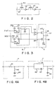
- Fig. 2 is a current diagram showing the detail construction of the one-stage section of a variable delay circuit shown in Fig. 1;
- Fig. 3 is a circuit diagram showing the detail construction of a phase comparator and a charge pump circuit shown in Fig. 1;
- Figs. 4A and 4B are circuit diagrams showing the detail construction of a low-pass filter shown in Fig. 1;
- Fig. 5 is a circuit diagram showing the detail construction of a level conversion circuit shown in Fig. 1;
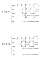
- Figs. 6 to 8 are timing charts showing the operation of a PLL section shown in Fig. 1;
- Fig. 9 is a characteristic diagram of the level conversion circuit of Fig. 5;
- Fig. 10 is a circuit diagram showing another detail construction of a level conversion circuit shown in Fig. 1;
- Fig. 11 is a characteristic diagram of the level conversion circuit of Fig. 10;
- Figs. 12 and 13 are circuit diagrams each showing still another detail construction of a level conversion circuit shown in Fig. 1;
- Fig. 14 is a current diagram showing another detail construction of the one-stage section of the variable delay circuit shown in Fig. 1;
- Figs. 15 and 16 are circuit diagrams showing the level conversion circuit of Fig. 1 in a case where the variable delay circuit of Fig. 14 is used;
- Fig. 17 is a circuit diagram showing the conventional voltage controlled circuit; and
- Fig. 18 is a block diagram showing the construction of a PLL frequency synthesizer type tuning system in which PLL section 1 and
VCO section 2 shown in Fig. 1 are used for the local oscillation section of a super heterodyne tuner. - There will now be described an embodiment of this invention with reference to the accompanying drawings.
- Fig. 1 is a block diagram showing the whole construction of a voltage controlled oscillator circuit according to one embodiment of this invention. In Fig. 1, 1 denotes a PLL section, and 2 denotes a VCO section. PLL section 1 is supplied with reference frequency signal Fref and reference voltage Vref and controls the feedback operation so as to set the delay time of
delay circuit 3 in the loop to a constant value, for example, one half period T of reference frequency signal Fref. -
VCO section 2 is supplied with control voltage Vcont and output voltage Voff of low-pass filter 7 of the phase-locked loop of PLL section 1, and oscillation frequency FVCO is determined by controlling the delay time of the ring oscillator circuit usingdelay circuit 10 based on the received control voltage (Vcont) and output voltage (Voff). - In PLL section 1, reference frequency signal Fref is supplied to the first input terminals of first
variable delay circuit 3 and phase comparator 4. Output DO of firstvariable delay circuit 3 is input to the other input terminal of phase comparator 4 via inverter 5. Phase comparator 4 compares the phases of the two input signals and controls first output CP or second output DP according to the comparison result. - Two outputs CP and DP are supplied to charge
pump circuit 6. The output ofcharge pump circuit 6 is supplied to low-pass filter (LPF) 7 whose output voltage Voff is supplied together with reference voltage Vref to firstlevel conversion circuit 8. Firstlevel conversion circuit 8 controls the voltage level of output PV according to the two input voltage levels, and output voltage PV is supplied as a delay time control signal tovariable delay circuit 3. - In
VCO section 2, output voltage Voff of low-pass filter 7 and control voltage Vcont are supplied to second level conversion circuit 9. Like firstlevel conversion circuit 8, second level conversion circuit 9 controls the voltage level of output PV according to the two input voltage levels. Output voltage PV is supplied as a delay time control signal to secondvariable delay circuit 10. - Inverter 11 is connected between the input and output terminals of second
variable delay circuit 10 to constitute a ring oscillator circuit. Second level conversion circuit 9, secondvariable delay circuit 10 and inverter 11 are formed with substantially the same constructions as firstlevel conversion circuit 8, firstvariable delay circuit 3 and inverter 5. - For example, each of
variable delay circuits Variable delay circuit 3 is formed of m-stage cascade-connected basic circuits andvariable delay circuit 10 is formed of n-stage cascade-connected basic circuits in this example. - An input signal is serially supplied via
first transfer gate 21 of a P-channel transistor,inverter 22,second transfer gate 23 of a P-channel transistor andinverter 24, and then output. The gates of first andsecond transfer gates second transfer gates - Fig. 3 is a circuit diagram showing the detail construction of phase comparator 4 and
charge pump circuit 6. In phase comparator 4, reference frequency signal Fref is supplied as a clock signal to D-type flip-flop 31. Likewise, output NDO of inverter 5 in Fig. 1 is supplied as a clock signal to D-type flip-flop 32. Q outputs of flip-flops gate 33 whose output is in turn supplied as a reset signal to flip-flops - Output Q of flip-
flop 31 is supplied as first output CP via inverter 34, and output Q of flip-flop 32 is supplied as output DP. -
Charge pump circuit 6 includes P-channel transistor 35 and N-channel transistor 36 series-connected between power source voltage terminal Vcc and the ground terminal. The gates oftransistors 35 and 36 are respectively supplied with first output CP and second output DP of phase comparator 4. - As shown in Fig. 4A, for example, low-
pass filter 7 includesresistors capacitor 43. It is also possible to constitute low-pass filter 7 byresistors capacitors - As shown in Fig. 5, for example, each of first and second
level conversion circuits 8 and 9 is constituted by two P-channel transistors channel transistor 53. - The source-drain path of P-
channel transistor 51 is connected between power source voltage terminal Vcc andnode 54 from which voltage PV is derived, and the gate oftransistor 51 is supplied with output voltage Voff of low-pass filter 7. - The source-drain path of P-
channel transistor 52 is connected between power source voltage terminal Vcc andnode 54, and the gate oftransistor 52 is connected tonode 54. The source-drain path of N-channel transistor 53 is connected betweennode 54 and the ground terminal. - In the case of first
level conversion circuit 8, the gate oftransistor 53 is supplied with reference voltage Vref, and in the case of second level conversion circuit 9, the gate oftransistor 53 is supplied with control voltage Vcont. - There will now be described the operation of PLL circuit section 1 of Fig. 1.
- As shown in the timing chart of Fig. 6, first output CP of phase comparator 4 is set at a high level ("H") when the delay time of
variable delay circuit 3 including the delay time of inverter 5 is shorter than T/2 (T is a period of reference frequency signal Fref). At this time, second output DP of phase comparator 4 is kept at a high level in a period by which the delay time is shorter than T/2. The high level portion of second output DP is supplied as a discharging pulse to chargepump circuit 6. - In
charge pump circuit 6, N-channel transistor 36 of Fig. 3 is set conductive in the high level period of output DP, thereby dischargingoutput 37. As a result, output voltage Voff of low-pass filter 7 is lowered. In this case, if reference voltage Vref is kept constant at a voltage equal to half power source voltage Vcc, output voltage PV oflevel conversion circuit 8 will rise. - Assume now that output voltage Voff of low-
pass filter 7 is supplied to the gate of P-channel transistor 51 and reference voltage Vref is supplied to the gate of N-channel transistor 53. Then, a current flowing into P-channel transistor 51 increases when voltage Voff is lowered as described above, and thus voltage PV ofnode 54 rises. As a result, the resistance components oftransfer gates variable delay circuit 3 of Fig. 2 increase, thereby increasing the delay time ofvariable delay circuit 3. - In contrast with the above case, when the delay time of
variable delay circuit 3 including the delay time of inverter 5 is longer than T/2 (T is a period of reference frequency signal Fref) as shown in the timing chart of Fig. 7, second output DP of phase comparator 4 is set at a low level ("L"). At this time, first output CP of phase comparator 4 is kept at a low level in a period by which the delay time is longer than T/2. The low level portion of first output CP is supplied as a charging pulse to chargepump circuit 6. - In
charge pump circuit 6, P-channel transistor 35 of Fig. 3 is set conductive in the low level period of output CP, thereby chargingoutput 37. As a result, output voltage Voff of low-pass filter 7 is raised. Thus, in this case, voltage PV ofnode 54 is lowered. As a result, the resistance components oftransfer gates variable delay circuit 3 of Fig. 2 decrease, thereby reducing the delay time ofvariable delay circuit 3. - When the delay time of first
variable delay circuit 3 is set equal to T/2 as shown in the timing chart of Fig. 8 and the PLL loop is set into the stable condition, outputs CP and DP of phase comparator 4 are respectively set at constant levels of "H" and "L". At this time, output PV of firstlevel conversion circuit 8 is set at a constant potential level and the delay time of firstvariable delay circuit 3 is kept constant. - By performing the above operation, the delay time of
variable delay circuit 3 can be precisely controlled. - In
VCO section 2, if control voltage Vcont is set at the same level as reference voltage Vref, the same inputs as those supplied to firstlevel conversion circuit 8 of PLL section 1 are supplied to second level conversion circuit 9. As a result, the delay time of each basic circuit in secondvariable delay circuit 10 becomes equal to that of each basic circuit in firstvariable delay circuit 3 of PLL section 1. - In this case, delay time t for each stage of the basic circuit in first
variable delay circuit 3 can be expressed as follows:
- Further, oscillation frequency FVCO of the ring oscillator circuit formed of second
variable delay circuit 10 and inverter 11 ofVCO section 2 can be expressed as follows:
- The following equation can be obtained by substituting equation (3) into equation (2).

- In this way, oscillation frequency FVCO of the ring oscillator circuit of
VCO section 2 can be determined only by a ratio of the values of n and m and reference frequency signal Fref. Therefore, the oscillation output with the stable center frequency can be obtained without receiving influence of variation in the manufacturing condition. Further, output PV of level conversion circuit 9 can be controlled by adequately changing the level of control voltage Vcont. Therefore, the delay time ofvariable circuit 10 can be changed so as to control oscillation frequency FVCO. - Fig. 9 shows an example of the characteristic of oscillation frequency signal FVCO (Hz) with respect to control voltage Vcont (V). In Fig. 9, values Vtha, Vthb and Vthc of control voltage Vcont at which characteristic curves a, b, and c start to rise are threshold voltages of N-
channel transistor 53 in the level conversion circuit of Fig. 5. That is, variation in the threshold voltage oftransistor 53 affects oscillation frequency signal FVCO as fluctuation in the manufacturing condition, and in general, the variation range is approx. 0.6 V. - The above characteristic can be obtained as follows. First, output voltage Voff of low-
pass filter 7 is applied to the gate of P-channel transistor 51 and control voltage Vcont is applied to the gate of N-channel transistor 53 of Fig. 5 in second level conversion circuit 9 ofVCO section 2. In this case,transistor 53 is kept nonconductive before control voltage Vcont exceeds the threshold voltage oftransistor 53. - At this time, assume that
transistor 51 supplied with voltage Voff is set in the conductive state. Then,transistor 52 is turned on if the potential difference between the gate and source thereof is larger than the threshold voltage of the P-channel transistor. However, voltage PV ofoutput node 54 is set at the Vcc level by means oftransistor 51 which is set in the conductive state. Therefore, the transfer gates (21, 23 in Fig. 2) in each basic circuit of variablesecond delay circuit 10 are turned off by output voltage PV. As a result, the ring oscillator circuit including secondvariable delay circuit 10 and inverter 11 will not oscillate. Therefore, as shown in Fig. 9, oscillation frequency signal FVCO becomes 0 (Hz). When control voltage Vcont has exceeded the threshold voltage oftransistor 53, characteristic curves a, b, and c start to rise. Each of characteristic curves a, b, and c passes center frequency Fc at which Vcont = Vref. - As described above, with the level conversion circuit having the construction of Fig. 5, a characteristic curve of oscillator frequency signal FVCO can be obtained which is first kept at a frequency of 0 Hz, starts to increase when Vcont has exceeded the threshold voltage of
transistor 53, and then passes preset center frequency Fc. - Assume now that Vcc is 5 (V), Vref is 2.5 (V), and threshold voltage Vth of N-
channel transistor 53 is 1.2 (V), and FVCO is set to 10 (MHz) when Vcont = Vref = 2.5 (V). Then, it is possible to realize a VCO circuit which has a variable frequency range of 0 to 10 (MHz) with respect to the range of Vcont from 0 to 2.5 (V). - In a case where the level conversion circuit of Fig. 5 is used as
level conversion circuits 8 and 9 in Fig. 1, the FVCO characteristic curve starts to abruptly rise when Vcont shown by the characteristic diagram of Fig. 9 has exceeded the threshold voltage oftransistor 53. That is, the inclination of each of characteristic curves a, b, and c becomes steeper and ΔFVCO/ΔVcont becomes relatively large. As a result, noise introduced from the exterior into the VCO circuit of Fig. 1 may cause ΔFVCO to significantly vary for a small amount of variation in ΔVcont, so that the oscillation frequency may fluctuate. Further, the variable range of Vcont is narrowed by threshold voltage VthN of the N-channel transistor with respect to the ground voltage. - In such a case, a circuit shown in Fig. 10 may be used as first and second
level conversion circuits 8 and 9 to solve the above problem. That is, the level conversion circuit of Fig. 10 further includes N-channel transistor 55 whose source-drain path is connected betweennode 54 and the ground terminal and whose gate is supplied with constant voltage E1. In this case, constant voltage E1 is set higher than the threshold voltage of N-channel transistor 55, andtransistor 55 is normally kept in the conductive state. - Since, in the level conversion circuit,
transistor 55 is normally kept in the conductive state, voltage PV tends to change from Vcc towards the ground voltage, and is set to a stable voltage level determined bytransistors transistor 55 is increased. Further, the variable range of Vcont can be widened to the ground voltage. - Fig. 12 is a circuit diagram showing the detail construction of the first and second level conversion circuits used in the VCO circuit in the above embodiment. In the case of the circuit of Fig. 12, the gate of N-
channel transistor 55 in the circuit of Fig. 10 is not connected to receive constant voltage E1 but is connected to the drain thereof oroutput node 54 for voltage PV. When the gate oftransistor 55 is supplied with substantially constant voltage E1 as shown in Fig. 10, a current flowing intotransistor 55 becomes constant andtransistor 55 functions as a constant current source. In contrast, when the gate oftransistor 55 is connected to the drain thereof as shown in Fig. 12,transistor 55 is normally kept in the conductive state and substantially the same characteristic as in the case of Fig. 11 can be obtained. - Fig. 13 is a circuit diagram showing the detail construction of first and second
level conversion circuits 8 and 9 used in the VCO circuit of the above embodiment. In the case of the circuit of Fig. 13, the gate of P-channel transistor 52 in the circuit of Fig. 5 is not connected tooutput node 54 for voltage PV but is connected to receive constant voltage E2. With this connection,transistor 52 is used as a constant current load. Also, in this example, the same characteristic as shown in Fig. 9 can be obtained. - Fig. 14 is a circuit diagram showing another construction of the basic circuit used in each of
variable delay circuits CMOS transfer gate 25 formed of P-channel and N-channel transistors,inverter 22, secondCMOS transfer gate 26 formed of P-channel and N-channel transistors, andinverter 24 and is then output. The gates of the P-channel transistors of first and secondCMOS transfer gates - The voltage level of delay time control signal NV is set to be higher or lower according as the voltage level of delay time control signal PV becomes lower or higher, respectively.
- Fig. 15 is a circuit diagram showing the detail construction of first and second
level conversion circuits 8 and 9 in the case wherevariable delay circuits - The circuit of Fig. 15 is constituted by additionally providing P-
channel transistor 56 and N-channel transistor 57 in the circuit of Fig. 5. The source-drain path of P-channel transistor 56 is connected between power source voltage Vcc andoutput node 58 for delay time control signal NV, and the gate thereof is connected tooutput node 54 for signal PV. Likewise, the source-drain path of N-channel transistor 57 is connected betweenoutput node 58 for signal NV and the ground terminal, and the gate thereof is connected tooutput node 58 for signal NV. Thus,transistors - In the level conversion circuit of Fig. 15, the amount of variation in signal NV with respect to the amount of variation in control voltage Vcont or reference voltage Vref supplied to the gate of
transistor 53 tends to decrease. Therefore, a difference will occur between the amounts of variation in signals PV and NV for the same amount of variation in reference voltage Vref or control voltage Vcont. As a result, the amount of variation in the gate voltage of the N-channel transistors of first and secondCMOS transfer gates - If the difference between the amounts of variation in signals PV and NV may cause serious problems, it is preferable to use a level conversion circuit with the construction shown in Fig. 16 instead of the level conversion circuit shown in Fig. 15. In the level conversion circuit of Fig. 16, in order to compensate for the reduction in the amounts of variation in signal NV, N-
channel transistor 59, P-channel transistor 60 and N-channel transistor 61 are additionally provided in the circuit of Fig. 15. - The source-drain path of
transistor 59 is connected betweenoutput node 58 for signal NV and the ground terminal. The source-drain path oftransistor 60 is connected between power source voltage terminal Vcc and gate node 62 oftransistor 59, and the gate thereof is connected to node 62. Further, the source-drain path of transistor 61 is connected between node 62 and the ground terminal, and the gate thereof is connected to receive reference voltage Vref or control voltage Vcont. - With the above level conversion circuit, when reference voltage Vref or control voltage Vcont rises, PV is lowered and NV is raised. At this time, a voltage of node 62 is lowered by means of an inverter formed of
transistors 60 and 61. As a result, a current flowing intotransistor 59 decreases. In this way,transistor 59 functions to raise NV so as to compensate for reduction in the amount of variation in NV. - The voltage controlled oscillation circuit according to the above embodiment is constituted by MOS transistors, but it is also possible to a voltage controlled oscillation circuit by use of bipolar transistors.
- Fig. 18 shows a PLL frequency synthesizer type tuning system including a voltage controlled oscillation circuit according to this invention. In the system of Fig. 18, PLL section 1 and
VCO section 2 of Fig. 1 are used in the local oscillator of a super heterodyne type tuner. The contruction of PLL section 1 andVCO section 2 may be the same as that of Fig. 1. - In Fig. 18, UHF or VHF television input signal Fin is input to super
heterodyne tuner 101. Intuner 101, the frequency of input signal Fin is lowered (or divided) by means of a prescaler to obtain a high frequency signal of a desired frequency, if necessary. The high frequency signal is frequency-converted to intermediate frequency signal PIF of a preset frequency, using a beat between the high frequency signal and oscillation output Fvco ofVCO section 2. - Control voltage Vcont for determining the oscillation frequency of
VCO section 2 can be derived fromband switching driver 102 and selectively set according to data Vcont from microcomputer (MPU) 200. - Reference frequency signal Fref supplied from
tuner 101 is input to PLL section 1, and output Voff of PLL section 1 is supplied toVCO section 2 via an LPF circuit. (In Fig. 18, since an LPF is separately provided outside PLL section 1,PLL 7 in Fig. 1 can be omitted). Reference voltage Vref supplied to PLL section 1 can be obtained by D/A converting data Vref fromMPU 200. - That is, when the user depresses a preset key of
key matrix 201 to specify a desired reception channel,LED display 202 displays the reception channel. When the channel specification is input toMPU 200,MPU 200 supplies data Vref and Vcont corresponding to the specified reception channel to PLL section 1 andband switching driver 102, according to the program and data stored inmemory 203. - For example, the channel specification may be effected by using a combination of
remote control transmitter 204 andremote control receiver 205. The results of various specification by the remote control are supplied to on-screen display driver 206. Then, the RGB circuit of a CRT (not shown) is driven by means ofdriver 206, and the result of color adjustment or reception channel specified by the remote control is displayed on the CRT. -
Tuner 101, switchingdriver 102, PLL section 1, LPF and the like are integrally formed astuner pack 100 and can be manufactured and adjusted independently from the circuit ofMPU 200. - As described above, according to this invention, the center frequency of the oscillation frequency can be determined by controlling the delay time of the variable delay circuit. Since the delay time can be precisely controlled by means of the phase-locked loop, a stable center frequency can be obtained without receiving any influence due to fluctuation in the manufacturing condition. Further, since the delay time is changed by the reference frequency signal, the center frequency can be freely set to a desired value and the frequency band of the oscillation frequency can also be freely set.
Claims (10)
a PLL section (1) for supplying a deviation signal (Voff) according to a received reference frequency signal (Fref) and a received reference voltage (Vref); and a VCO section (2) for supplying an oscillation output (Fvco) according to the deviation signal (Voff) and received control voltage (Vcont);
said PLL section (1) comprising:
first delay means (3, 5) for delaying the reference frequency signal (Fref) according to a preset first delay control signal (PV from 8) and outputting a delay signal (ND0);
phase difference detection means (4, 6, 7) for comparing the phase of the reference frequency signal (Fref) with that of the delay signal (ND0) and outputting the deviation signal (Voff) based on the phase difference; and
first delay control means (8) for outputting the first delay control signal (PV from 8) having a signal level corresponding to the preset reference voltage (Vref) and the deviation signal (Voff).
second delay control means (9) for outputting a second delay control signal (PV from 9) producing a signal level corresponding to the control voltage (Vcont) and the deviation signal (Voff); and
second delay means (10, 11) for cyclically delaying the oscillation output (Fvco) according to the second delay control signal (PV form 9) and generating the oscillation output (Fvco).
a plurality of transmission gates (21, 23); and a plurality of inverters (22, 24) alternately series-connected to said plurality of transmission gates (21, 23); and
the first delay control signal (PV from 8) is used as gate inputs of said plurality of transmission gates (21, 23).
a plurality of transmission gates (21, 23); and a plurality of inverters (22, 24) alternately series-connected to said plurality of transmission gates (21, 23); and
the second delay control signal (PV from 9) is used as gate inputs of said plurality of transmission gates (21, 23).
a plurality of CMOS transmissicn gates (25, 26); and a plurality of inverters (22, 24) alternately series-connected to said plurality of CMOS transmission gates (25, 26); and
the first delay control signal (PV from 8) is used as gate inputs of one channel (P) type gates of said plurality of CMOS transmission gates (25, 26) and an inverted signal (NV) of the first delay control signal (PV from 8) is used as gate inputs of the other channel (N) type gates of said plurality of CMOS transmission gates (25, 26).
a plurality of CMOS transmission gates (25, 26); and a plurality of inverters (22, 24) alternately series-connected to said plurality of CMOS transmission gates (25, 26); and
the second delay control signal (PV from 9) is used as gate inputs of one channel (P) type gates of said plurality of CMOS transmission gates (25, 26) and an inverted signal (NV) of the second delay control signal (PV from 9) is used as gate inputs of the other channel (N) type gates of said plurality of CMOS transmission gates (25, 26).
a first D-type flip-flop (31) clocked by the reference frequency signal (Fref);
a second D-type flip-flop (32) clocked by the delay signal (ND0);
means (33) for resetting said first and second D-type flip-flops (31, 32) according to the logical product of Q outputs of said first and second D-type flip-flops (31, 32);
a first transistor (35) of a first conductivity type (P) driven by an inverted signal (CP) of the Q output of said first D-type flip-flop (31);
a second transistor (36) of a second conductivity type (N) driven by the Q output signal (DP) of said second D-type flip-flop (32); and
means (7) for deriving the deviation signal (Voff) from a signal (37) which is obtained by combining outputs of said first and second transistors (35, 36).
a first MOS transistor (51) of a first conductivity type (P) having a gate supplied with the deviation signal (Voff), a source connected to a first power source circuit (Vcc) and a drain for outputting the first delay control signal (PV from 8);
a second MOS transistor (52) of the first conductivity type (P) having a source connnected to said first power source circuit (Vcc) and a drain and a gate connected to the drain of said first MOS transistor (51); and
a third MOS transistor (53) of a second conductivity type (N) having a gate supplied with the reference voltage (Vref), a source connected to a second power source circuit (Vss) and a drain connected to the drain of said first MOS transistor (51).
Applications Claiming Priority (2)
| Application Number | Priority Date | Filing Date | Title |
|---|---|---|---|
| JP63119701A JP2531742B2 (en) | 1988-05-17 | 1988-05-17 | Voltage controlled oscillator |
| JP119701/88 | 1988-05-17 |
Publications (3)
| Publication Number | Publication Date |
|---|---|
| EP0342626A2 true EP0342626A2 (en) | 1989-11-23 |
| EP0342626A3 EP0342626A3 (en) | 1990-09-26 |
| EP0342626B1 EP0342626B1 (en) | 1994-07-20 |
Family
ID=14767940
Family Applications (1)
| Application Number | Title | Priority Date | Filing Date |
|---|---|---|---|
| EP89108840A Expired - Lifetime EP0342626B1 (en) | 1988-05-17 | 1989-05-17 | Voltage controlled oscillator circuit |
Country Status (6)
| Country | Link |
|---|---|
| US (1) | US4912433A (en) |
| EP (1) | EP0342626B1 (en) |
| JP (1) | JP2531742B2 (en) |
| KR (1) | KR920004335B1 (en) |
| DE (1) | DE68916854T2 (en) |
| HK (1) | HK83395A (en) |
Cited By (6)
| Publication number | Priority date | Publication date | Assignee | Title |
|---|---|---|---|---|
| EP0520558A1 (en) * | 1991-06-27 | 1992-12-30 | Koninklijke Philips Electronics N.V. | Phase locked loop and digital phase comparator for use in a phase-locked loop |
| US5672248A (en) * | 1994-04-12 | 1997-09-30 | Kimberly-Clark Worldwide, Inc. | Method of making soft tissue products |
| WO1998010519A1 (en) * | 1996-09-04 | 1998-03-12 | Siemens Aktiengesellschaft | Low-jitter phase-locking loop |
| US6017417A (en) * | 1994-04-12 | 2000-01-25 | Kimberly-Clark Worldwide, Inc. | Method of making soft tissue products |
| CN1050020C (en) * | 1994-06-24 | 2000-03-01 | 陈万元 | Random pulse time delay locking direction |
| EP1265364A1 (en) * | 2001-05-29 | 2002-12-11 | STMicroelectronics, Inc. | Precision closed loop delay line for wide frequency data recovery |
Families Citing this family (31)
| Publication number | Priority date | Publication date | Assignee | Title |
|---|---|---|---|---|
| JPH0396015A (en) * | 1989-09-08 | 1991-04-22 | Oki Electric Ind Co Ltd | High speed digital pll device |
| FR2658015B1 (en) * | 1990-02-06 | 1994-07-29 | Bull Sa | LOCKED PHASE CIRCUIT AND RESULTING FREQUENCY MULTIPLIER. |
| US6150855A (en) * | 1990-02-06 | 2000-11-21 | Bull, S.A. | Phase-locked loop and resulting frequency multiplier |
| FR2664769A1 (en) * | 1990-07-11 | 1992-01-17 | Bull Sa | DATA SAMPLING DEVICE AND DATA DIGITAL TRANSMISSION SYSTEM THEREOF. |
| FR2664765B1 (en) * | 1990-07-11 | 2003-05-16 | Bull Sa | DEVICE FOR SERIALIZATION AND DESERIALIZATION OF DATA AND SYSTEM FOR DIGITAL TRANSMISSION OF SERIAL DATA THEREOF. |
| FR2664770A1 (en) * | 1990-07-11 | 1992-01-17 | Bull Sa | METHOD AND SYSTEM FOR DIGITAL DATA TRANSMISSION IN SERIES. |
| JP2597739B2 (en) * | 1990-08-24 | 1997-04-09 | 株式会社東芝 | Signal delay circuit, clock signal generation circuit, and integrated circuit system |
| DE69130043T2 (en) * | 1990-09-18 | 1999-04-15 | Fujitsu Ltd | Electronic arrangement with a reference delay generator |
| US5142696A (en) * | 1991-04-16 | 1992-08-25 | Motorola, Inc. | Current mirror having increased output swing |
| US5150078A (en) * | 1991-11-29 | 1992-09-22 | Hughes Aircraft Company | Low noise fine frequency step synthesizer |
| US8352400B2 (en) | 1991-12-23 | 2013-01-08 | Hoffberg Steven M | Adaptive pattern recognition based controller apparatus and method and human-factored interface therefore |
| US5903454A (en) | 1991-12-23 | 1999-05-11 | Hoffberg; Linda Irene | Human-factored interface corporating adaptive pattern recognition based controller apparatus |
| US6850252B1 (en) | 1999-10-05 | 2005-02-01 | Steven M. Hoffberg | Intelligent electronic appliance system and method |
| US6418424B1 (en) | 1991-12-23 | 2002-07-09 | Steven M. Hoffberg | Ergonomic man-machine interface incorporating adaptive pattern recognition based control system |
| US10361802B1 (en) | 1999-02-01 | 2019-07-23 | Blanding Hovenweep, Llc | Adaptive pattern recognition based control system and method |
| US6400996B1 (en) | 1999-02-01 | 2002-06-04 | Steven M. Hoffberg | Adaptive pattern recognition based control system and method |
| US5552733A (en) * | 1993-01-19 | 1996-09-03 | Credence Systems Corporation | Precise and agile timing signal generator based on a retriggered oscillator |
| US5317284A (en) * | 1993-02-08 | 1994-05-31 | Hughes Aircraft Company | Wide band, low noise, fine step tuning, phase locked loop frequency synthesizer |
| US5391996A (en) * | 1993-11-19 | 1995-02-21 | General Instrument Corporation Of Delaware | Techniques for generating two high frequency signals with a constant phase difference over a wide frequency band |
| JP3703516B2 (en) * | 1994-04-25 | 2005-10-05 | セイコーインスツル株式会社 | Oscillator circuit |
| US5621705A (en) * | 1994-05-02 | 1997-04-15 | Colorado Seminary | Programmable timing unit for generating multiple coherent timing signals |
| JP2771464B2 (en) * | 1994-09-29 | 1998-07-02 | 日本電気アイシーマイコンシステム株式会社 | Digital PLL circuit |
| EP0731560B1 (en) * | 1995-03-07 | 2003-05-28 | STMicroelectronics S.r.l. | Wide frequency range VCO with low jitter |
| WO1998019395A1 (en) * | 1995-06-19 | 1998-05-07 | Advantest Corporation | Delay time control circuit |
| JP3839081B2 (en) * | 1995-08-21 | 2006-11-01 | 富士通株式会社 | Oscillator |
| US5684421A (en) * | 1995-10-13 | 1997-11-04 | Credence Systems Corporation | Compensated delay locked loop timing vernier |
| US5801566A (en) * | 1996-04-03 | 1998-09-01 | Mitsubishi Electric Semiconductor Software Co., Ltd. | System clock generating circuit for a semiconductor device |
| JP3519894B2 (en) * | 1997-02-17 | 2004-04-19 | 富士通株式会社 | Oscillator |
| JP2000013204A (en) * | 1998-06-18 | 2000-01-14 | Fujitsu Ltd | Delay circuit and oscillation circuit using the delay circuit |
| US7966078B2 (en) | 1999-02-01 | 2011-06-21 | Steven Hoffberg | Network media appliance system and method |
| CN104601166B (en) * | 2015-01-23 | 2017-08-25 | 北京大学 | It is a kind of that there is the delay locked loop circuit for starting control function |
Citations (4)
| Publication number | Priority date | Publication date | Assignee | Title |
|---|---|---|---|---|
| JPS5555621A (en) * | 1978-10-18 | 1980-04-23 | Matsushita Electric Ind Co Ltd | Oscillator |
| EP0103404A2 (en) * | 1982-08-30 | 1984-03-21 | Xerox Corporation | Self-calibrated clock and timing signal generator |
| JPS6080316A (en) * | 1983-10-11 | 1985-05-08 | Hitachi Ltd | Voltage controlled oscillator |
| US4641048A (en) * | 1984-08-24 | 1987-02-03 | Tektronix, Inc. | Digital integrated circuit propagation delay time controller |
Family Cites Families (11)
| Publication number | Priority date | Publication date | Assignee | Title |
|---|---|---|---|---|
| US3614649A (en) * | 1969-12-24 | 1971-10-19 | Reaction Instr Inc | Frequency stabilization of continuously tunable oscillators |
| US4091335A (en) * | 1976-12-13 | 1978-05-23 | Texas Instruments Incorporated | Phase locked loop using current controlled ring oscillator |
| US4131861A (en) * | 1977-12-30 | 1978-12-26 | International Business Machines Corporation | Variable frequency oscillator system including two matched oscillators controlled by a phase locked loop |
| JPS5537031A (en) * | 1978-09-07 | 1980-03-14 | Trio Kenwood Corp | Phase synchronizing circuit |
| US4336505A (en) * | 1980-07-14 | 1982-06-22 | John Fluke Mfg. Co., Inc. | Controlled frequency signal source apparatus including a feedback path for the reduction of phase noise |
| JPS57174927A (en) * | 1981-04-21 | 1982-10-27 | Fujitsu Ltd | Skew adjusting circuit |
| JPS61105111A (en) * | 1984-10-27 | 1986-05-23 | Toshiba Corp | Voltage controlled oscillating circuit |
| JPS61107810A (en) * | 1984-10-31 | 1986-05-26 | Toshiba Corp | Voltage controlled oscillating circuit |
| JPH0752838B2 (en) * | 1985-03-20 | 1995-06-05 | 株式会社日立製作所 | Integrated circuit |
| US4829545A (en) * | 1986-08-25 | 1989-05-09 | Guzik Technical Enterprises, Inc. | Method and apparatus for data window centering ina multifrequency data separator |
| JPH021620A (en) * | 1987-11-30 | 1990-01-05 | Toshiba Corp | Voltage controlled oscillation circuit |
-
1988
- 1988-05-17 JP JP63119701A patent/JP2531742B2/en not_active Expired - Fee Related
-
1989
- 1989-05-16 US US07/352,540 patent/US4912433A/en not_active Expired - Lifetime
- 1989-05-17 DE DE68916854T patent/DE68916854T2/en not_active Expired - Fee Related
- 1989-05-17 KR KR1019890006579A patent/KR920004335B1/en not_active IP Right Cessation
- 1989-05-17 EP EP89108840A patent/EP0342626B1/en not_active Expired - Lifetime
-
1995
- 1995-05-25 HK HK83395A patent/HK83395A/en not_active IP Right Cessation
Patent Citations (4)
| Publication number | Priority date | Publication date | Assignee | Title |
|---|---|---|---|---|
| JPS5555621A (en) * | 1978-10-18 | 1980-04-23 | Matsushita Electric Ind Co Ltd | Oscillator |
| EP0103404A2 (en) * | 1982-08-30 | 1984-03-21 | Xerox Corporation | Self-calibrated clock and timing signal generator |
| JPS6080316A (en) * | 1983-10-11 | 1985-05-08 | Hitachi Ltd | Voltage controlled oscillator |
| US4641048A (en) * | 1984-08-24 | 1987-02-03 | Tektronix, Inc. | Digital integrated circuit propagation delay time controller |
Non-Patent Citations (2)
| Title |
|---|
| PATENT ABSTRACTS OF JAPAN, vol. 4, no. 87 (E-016), 6th June 1980; & JP-A-55 055 621 (MATSUSHITA ELECTRIC IND. CO., LTD) 23-04-1980 * |
| PATENT ABSTRACTS OF JAPAN, vol. 9, no. 220 (E-341), 6th September 1985; & JP-A-60 080 316 (HITACHI SEISAKUSHO K.K.) 08-05-1985 * |
Cited By (7)
| Publication number | Priority date | Publication date | Assignee | Title |
|---|---|---|---|---|
| EP0520558A1 (en) * | 1991-06-27 | 1992-12-30 | Koninklijke Philips Electronics N.V. | Phase locked loop and digital phase comparator for use in a phase-locked loop |
| US5672248A (en) * | 1994-04-12 | 1997-09-30 | Kimberly-Clark Worldwide, Inc. | Method of making soft tissue products |
| US6017417A (en) * | 1994-04-12 | 2000-01-25 | Kimberly-Clark Worldwide, Inc. | Method of making soft tissue products |
| CN1050020C (en) * | 1994-06-24 | 2000-03-01 | 陈万元 | Random pulse time delay locking direction |
| WO1998010519A1 (en) * | 1996-09-04 | 1998-03-12 | Siemens Aktiengesellschaft | Low-jitter phase-locking loop |
| EP1265364A1 (en) * | 2001-05-29 | 2002-12-11 | STMicroelectronics, Inc. | Precision closed loop delay line for wide frequency data recovery |
| US6985016B2 (en) | 2001-05-29 | 2006-01-10 | Stmicroelectronics, Inc. | Precision closed loop delay line for wide frequency data recovery |
Also Published As
| Publication number | Publication date |
|---|---|
| EP0342626B1 (en) | 1994-07-20 |
| DE68916854D1 (en) | 1994-08-25 |
| KR900019371A (en) | 1990-12-24 |
| JPH0289422A (en) | 1990-03-29 |
| JP2531742B2 (en) | 1996-09-04 |
| HK83395A (en) | 1995-06-01 |
| EP0342626A3 (en) | 1990-09-26 |
| DE68916854T2 (en) | 1994-12-08 |
| US4912433A (en) | 1990-03-27 |
| KR920004335B1 (en) | 1992-06-01 |
Similar Documents
| Publication | Publication Date | Title |
|---|---|---|
| EP0342626B1 (en) | Voltage controlled oscillator circuit | |
| US4987387A (en) | Phase locked loop circuit with digital control | |
| US5565817A (en) | Ring oscillator having accelerated charging and discharging of capacitors | |
| US5923715A (en) | Digital phase-locked loop circuit | |
| US6392494B2 (en) | Frequency comparator and clock regenerating device using the same | |
| US5487093A (en) | Autoranging digital analog phase locked loop | |
| US7292079B2 (en) | DLL-based programmable clock generator using a threshold-trigger delay element circuit and a circular edge combiner | |
| US20030042985A1 (en) | Phase synchronizing circuit | |
| KR910008514B1 (en) | Redrivable multivibrator | |
| JPH0799807B2 (en) | Phase synchronization circuit | |
| US4859970A (en) | Voltage controlled oscillator | |
| US7443254B2 (en) | Relaxation oscillator with propagation delay compensation for improving the linearity and maximum frequency | |
| EP0613246A1 (en) | Wide-range variable delay line and ring oscillator | |
| US7106142B2 (en) | Ring-type voltage oscillator with improved duty cycle | |
| US8816782B2 (en) | Phase locked loop circuit having a voltage controlled oscillator with improved bandwidth | |
| EP0379169B1 (en) | Signal delay circuit using charge pump circuit | |
| US10623005B2 (en) | PLL circuit and CDR apparatus | |
| JPH11163636A (en) | Output stage, charge pump, demodulator and radio telephone device | |
| US7015766B1 (en) | CMOS voltage-controlled oscillator (VCO) with a current-adaptive resistor for improved linearity | |
| US6188285B1 (en) | Phase-locked loop circuit and voltage-controlled oscillator capable of producing oscillations in a plurality of frequency ranges | |
| US5457429A (en) | Ring oscillator circuit for VCO | |
| EP0755120A1 (en) | Phase-locked loop circuit | |
| US8081040B1 (en) | Method and apparatus for oscillating | |
| US20100117741A1 (en) | PLL Circuit | |
| JP2001024485A (en) | Pll circuit |
Legal Events
| Date | Code | Title | Description |
|---|---|---|---|
| PUAI | Public reference made under article 153(3) epc to a published international application that has entered the european phase |
Free format text: ORIGINAL CODE: 0009012 |
|
| 17P | Request for examination filed |
Effective date: 19890517 |
|
| AK | Designated contracting states |
Kind code of ref document: A2 Designated state(s): DE FR GB |
|
| PUAL | Search report despatched |
Free format text: ORIGINAL CODE: 0009013 |
|
| RHK1 | Main classification (correction) |
Ipc: H03L 7/081 |
|
| AK | Designated contracting states |
Kind code of ref document: A3 Designated state(s): DE FR GB |
|
| 17Q | First examination report despatched |
Effective date: 19930730 |
|
| GRAA | (expected) grant |
Free format text: ORIGINAL CODE: 0009210 |
|
| AK | Designated contracting states |
Kind code of ref document: B1 Designated state(s): DE FR GB |
|
| REF | Corresponds to: |
Ref document number: 68916854 Country of ref document: DE Date of ref document: 19940825 |
|
| ET | Fr: translation filed | ||
| PLBE | No opposition filed within time limit |
Free format text: ORIGINAL CODE: 0009261 |
|
| STAA | Information on the status of an ep patent application or granted ep patent |
Free format text: STATUS: NO OPPOSITION FILED WITHIN TIME LIMIT |
|
| 26N | No opposition filed | ||
| PGFP | Annual fee paid to national office [announced via postgrant information from national office to epo] |
Ref country code: GB Payment date: 19970508 Year of fee payment: 9 |
|
| PGFP | Annual fee paid to national office [announced via postgrant information from national office to epo] |
Ref country code: FR Payment date: 19970513 Year of fee payment: 9 |
|
| PG25 | Lapsed in a contracting state [announced via postgrant information from national office to epo] |
Ref country code: GB Free format text: LAPSE BECAUSE OF NON-PAYMENT OF DUE FEES Effective date: 19980517 |
|
| PG25 | Lapsed in a contracting state [announced via postgrant information from national office to epo] |
Ref country code: FR Free format text: LAPSE BECAUSE OF NON-PAYMENT OF DUE FEES Effective date: 19980531 |
|
| GBPC | Gb: european patent ceased through non-payment of renewal fee |
Effective date: 19980517 |
|
| REG | Reference to a national code |
Ref country code: FR Ref legal event code: ST |
|
| PGFP | Annual fee paid to national office [announced via postgrant information from national office to epo] |
Ref country code: DE Payment date: 20060511 Year of fee payment: 18 |
|
| PG25 | Lapsed in a contracting state [announced via postgrant information from national office to epo] |
Ref country code: DE Free format text: LAPSE BECAUSE OF NON-PAYMENT OF DUE FEES Effective date: 20071201 |