EP0343602A2 - Microwave plasma treating apparatus - Google Patents
Microwave plasma treating apparatus Download PDFInfo
- Publication number
- EP0343602A2 EP0343602A2 EP89109283A EP89109283A EP0343602A2 EP 0343602 A2 EP0343602 A2 EP 0343602A2 EP 89109283 A EP89109283 A EP 89109283A EP 89109283 A EP89109283 A EP 89109283A EP 0343602 A2 EP0343602 A2 EP 0343602A2
- Authority
- EP
- European Patent Office
- Prior art keywords
- microwave
- cavity resonator
- treating apparatus
- disposed
- gas
- Prior art date
- Legal status (The legal status is an assumption and is not a legal conclusion. Google has not performed a legal analysis and makes no representation as to the accuracy of the status listed.)
- Granted
Links
Images


Classifications
-
- H—ELECTRICITY
- H01—ELECTRIC ELEMENTS
- H01J—ELECTRIC DISCHARGE TUBES OR DISCHARGE LAMPS
- H01J37/00—Discharge tubes with provision for introducing objects or material to be exposed to the discharge, e.g. for the purpose of examination or processing thereof
- H01J37/32—Gas-filled discharge tubes
- H01J37/32009—Arrangements for generation of plasma specially adapted for examination or treatment of objects, e.g. plasma sources
- H01J37/32357—Generation remote from the workpiece, e.g. down-stream
-
- H—ELECTRICITY
- H05—ELECTRIC TECHNIQUES NOT OTHERWISE PROVIDED FOR
- H05H—PLASMA TECHNIQUE; PRODUCTION OF ACCELERATED ELECTRICALLY-CHARGED PARTICLES OR OF NEUTRONS; PRODUCTION OR ACCELERATION OF NEUTRAL MOLECULAR OR ATOMIC BEAMS
- H05H1/00—Generating plasma; Handling plasma
- H05H1/24—Generating plasma
- H05H1/46—Generating plasma using applied electromagnetic fields, e.g. high frequency or microwave energy
Definitions
- the present invention relates to a microwave plasma treating apparatus and a control system therein. More specifically, it relates to an improved microwave plasma treating apparatus suitable for forming a deposited film and etching an object.
- plasma CVD method plasma chemical vapor deposition methods
- plasma CVD apparatus apparatuses for practicing those plasma CVD methods
- the plasma CVD methods as they have advantages such as (i) capable of forming a deposited film at a low temperature of from 200 to 400°C, (ii) requiring no heat resistance for a substrate, etc.
- a silicon dioxide film or a silicon nitride film which is usable as an insulating film in semiconductor systems
- an amorphous silicon (a-Si) film which is usable in solar cells, close- contact type image sensors or photosensitive drums, a diamond thin film, etc.
- RF radiowave
- the conventional RF plasma CVD method involves the following drawbacks on the other hand. That is, ion sheath is apt to form on the side of a substrate to develop a negative self-bias, by which ion species in the plasma is drawn to the cathode to moderate the incident impact shock of the ion species to the anode on which the substrate is disposed. However, the ion species is still applied to the surface of the substrate and mixed into the deposited film to bring about internal stresses or increase the defect density, failing to obtain a deposited film of good quality. In addition, since the electron density is as low as from 108 to 1010, the decomposing efficiency of the starting material gas is not so high and the deposition rate is low. Further in addition, since the electron temperature is as low as - 4 eV, starting material gas of high bonding energy such as silicon halide compound is less decomposable.
- type 1 MW-plasma treating apparatus a gas pipe is inserted through or placed in contact with a rectangular or coaxial waveguide to form a plasma (hereinafter referred to as "type 1 MW-plasma treating apparatus").
- the other one is of a type as disclosed in Japanese Patent Laid-Open No. 57-133636, in which electron cyclotron resonance (ECR) is established within a cavity resonator and a plasma is drawn out by a divergent magnetic field (hereinafter referred to as "type 2 MW-plasma treating apparatus").
- ECR electron cyclotron resonance
- Fig. 3 shows a typical type 1-MW-plasma treating apparatus (refer to Japanese Utility Model Publication No. 62-36240).
- the type 1 MW-plasma treating apparatus comprises a vacuum system, an exhaust system and a microwave introducing system as shown in Fig. 3.
- the vacuum system comprises a reactor 307, and a microwave transmissive tube or a window (for example, made of quartz tube) having an inside diameter on the order of 40 mm and connected by a gas introducing pipe 307a.
- the quartz tube (or the window) is connected to a first gas introducing pipe and is arranged perpendicularly to a microwave waveguide.
- a second gas introducing pipe is connected to the inside of the reactor 307 and a gas (silane gas) supplied is exhausted through an exhaust system (307b and 308).
- the gas introduced through the first gas introducing pipe (O2 gas or N2 gas) is converted into a plasma by microwave discharge.
- microwave input impedance can be matched by moving a sliding short-circuit plate, i.e., a plunger 305. Radicals of the plasma thus produced react with the silane gas supplied through the second gas introducing pipe, whereby a silicon dioxide film or a silicon nitride film is formed over the surface of a substrate 309.
- Fig. 4 shows a typical type 2 MW-plasma treating apparatus (refer to Japanese Patent Laid-Open No. 57-133636).
- the system and configuration of this apparatus are the same as those of the foregoing type 1 MW-plasma treating apparatus except for the discharging space for which an electromagnet 407 is used. That is, the vacuum system comprises a cylindrical plasma producing vessel 401 and a reactor 402 connected thereto, in which a microwave introducing window 403 is attached hermetically to the plasma producing vessel.
- a first gas introducing pipe 406 and a microwave waveguide 404 are connected to the plasma producing vessel 401.
- the plasma producing vessel 401 is water-cooled by means of a water-cooling pipe 405 disposed at the outer circumference thereof.
- the apparatus shown in Fig. 4 is provided with an electromagnet 407 disposed coaxially with the plasma producing vessel 401.
- a second gas introducing pipe and the exhaust system are connected to the reactor 402, and gases within the deposition vessel are exhausted by the exhaust system.
- a gas (H2 gas) introduced through the first gas introducing pipe 406 is formed into a plasma by electric discharge caused by the microwave energy.
- the magnetic flux density of the magnetic field is 875 gauss, the reflected wave of the microwave energy is almost zero.
- the end plate 411 of the cavity resonator having the construction of a choke is moved under vacuum depending on the type of the gas, the pressure of the gas and the microwave power applied, so that the cavity resonator meets required conditions.
- Radicals in the plasma are transported under an electron cyclotron motion in the direction of the lines of magnetic force, and the radicals in the plasma react with the gas (silane gas) introduced through the second gas introducing pipe to form an a-Si film over the surface of a substrate 408.
- gas silane gas
- both the type 1 MW-plasma treating apparatus and the type 2 MW-plasma treating apparatus have the following problems to be solved.
- the type 1 MW-plasma treating apparatus involves the following drawbacks; (i) it is necessary to control the pressure during electric discharge to an order of about 0.05 Torr or higher, or to a gas of such a type as having a large ionizing cross sectional area easily causing electric discharge in order to attain stable discharge: and (ii) in the case where the appratus is used for the film deposition, when the charged microwave power is increased in order to increase the film deposition rate, an electric field is concentrated to the junction between the quartz tube and the waveguide to cause sputtering to the quartz tube, by which impurities formed by the sputtering are mixed into the deposited film, failing to obtain a deposited film of satisfactory property.
- the type 1 MW-plasma treating apparatus is free from the sputtering problem as described above and discharge even in a low pressure region of about 10 ⁇ 4 Torr is possible.
- Another object of the present invention is to overcome the foregoing problems in the conventional microwave plasma treating apparatus and provide a microwave plasma treating apparatus capable of conducting dry etching to an object to be treated at good operationability and productivity.
- a further.object of the present invention is to provide a microwave plasma treating apparatus capable of stable electric discharge without using a large electromagnet as in the ECR system, in a low pressure region irrespective of the type of gas with small ionizing cross sectional area, while suppressing the reflected power, and at a low electric power.
- the microwave plasma treating apparatus according to the present invention for attaining the foregoing objects have the following constitutions.
- the microwave plasma treating apparatus comprising a vacuum vessel, means for introducing a microwave by way of a microwave transmission circuit to the inside of the vacuum vessel, means for supplying starting material gas to the inside of the vacuum vessel, means for evacuating the inside of the vacuum vessel and a specimen holder for maintaining a specimen substrate at the inside of the vacuum vessel, wherein a cavity resonator integrated with two matching circuits is disposed in the microwave transmission circuit and a magnetic field generator is disposed to the outside of the cavity resonator.
- the main features of the apparatus according to the present invention resides in the following points (a) through (c). Specifically, (a) matching is facilitated by a plunger for adjusting the axial length of the cavity resonator and a matching circuit by a cylindrical sliding type irises, E-H tuner or three-stub tuner disposed at the portion of the cylindrical cavity resonator for the microwave is introduced, (b) a bell jar is penetrated into the cavity resonator to excite TM mode and (c) a magnetic field generator is disposed to the outside of the cavity resonator to prepare a region of a high magnetic flux density in the electric discharging space at the inside of the cavity resonator.
- the apparatus according to the present invention can be desirably used for effectively forming a desired functional deposited thin film or for dry etching an object, which enables one to form semiconductor films or insulating films respectively of good quality, or to produce various etched materials, with good productivity and at a reduced cost.
- the microwave plasma treating apparatus having the foregoing constitutions according to the present invention is to be explained below while mainly referring to the above-mentioned features (a), (b) and (c).
- a constitution of the apparatus regarding the feature (a) can be attained by providing two matching circuits capable of being adjusted properly according to the phase and amplitude of a microwave. Since the energy of a standing wave is accumulated between the matching circuits and the cavity resonator, it is desirable that the distance between the matching circuits and the cavity resonator is reduced to the least possible extent. Most desirably, the matching circuits and the cavity resonator are integrated and at least one of the matching circuits is used as a plunger for varying the cavity length.
- phase and amplitude of the reflected microwave are dependent primarily on the plasma density and the morphology of a microwave feed circuit.
- the plasma density changes dependent on the kind of the gas, gas pressure or microwave power introduced and the complex refractive index n-ik (0 ⁇ n ⁇ 1; k is absorption coefficient) also changes correspondingly. Accordingly, for always maintaining the function of the cavity resonator, the effects of n and k has to be nullified.
- the cavity length (L) of the cavity resonator may be increased by a length equivalent to the reduction of the inside diameter of the cavity to n times (0 ⁇ n ⁇ 1) the original length.
- the effect of n can be nullified by varying the length (L) of the cavity resonator according to the variation of n .
- the effect of k namely, the effects of the amplitude and phase lag ⁇ of the reflected wave, can be nullified by adjusting the two matching circuits.
- the length (L) of the cavity resonator and the position of sliding matching irises may be adjusted for one set of ( n and k ).
- the reflected wave which are dependent on the morphology of the microwave feed circuit, can be matched efficiently by using the two matching circuits.
- a constitution relating to the aforesaid feature (b) can be attained by connecting a rectangular waveguide and a cylindrical cavity resonator with the axes thereof intersecting each other at a right angle as shown in Fig. 1.
- the waveguide and the cavity resonator are thus connected, an operation for varying the length of the cavity resonator is not obstructed by the waveguide.
- the microwave is driven in Tm 01n (n is a natural number), and the length of the cavity resonator can be changed even in the atmosphere, thereby facilitating the efficiency of operation.
- a constitution regarding the aforesaid feature (c) can be attained by disposing a tubular cylindrical magnetic field generator to the outside of the cavity resonator, by which a region of high magnetic flux density can be formed in the electric discharging space at the inside of the cavity resonator.
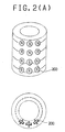
- the magnetic field generator is generally classified into a permanent magnet and an electromagnet. Specifically, there are permanent magnets disposed in a coaxial manner as shown in Figs. 2 (A) through (D), ring-like permanent magnets disposed as shown in Figs. 2(E) and (F), and electromagnets comprising air-cored solenoid coils as shown in Figs. 2(G) and (H). In each of Figs.
- the upper view is a side elevational view and the lower view is a top plan view each in a schematic manner, in which N and S mean magnetic poles.
- the permanent magnet those having great coercive force and residual magnetic flux density are suitable and, among all, rare earth or ferrite series magnets are preferred.
- the electromagnets those having central magnetic flux density of greater than 50 gauss and, more preferably, greater than 100 gauss are desirable. Electromagnets are combined by one set in Fig. 2(G) and by two sets in Fig. 2(H). Particularly, in the embodiment shown in Fig. 2(H), it is possible to change the magnetic poles by changing the polarity of cuttent for the two sets of electromagnets, thereby obtaining a mirror type or cusped type magnetic field.
- the magnetic flux density in the electric discharging space of the magnetic field generator used for the microwave plasma treating apparatus according to the present invention is such a magnetic flux density as capable of obtaining electron cyclotron resonance relative to the frequency of the microwave.
- desired magnetic flux density can be obtained by controlling the electric current supplied thereto.
- the performance of the microwave plasma treating apparatus is improved remarkably thereby enabling to lower the pressure during electric discharge, reduce the reflected power and save in the electric power for maintaining the electric discharge.
- FIG. 1 One embodiment for the apparatus according to the present invention is shown as a schematic perspective view in Fig. 1.
- Fig. 1 In Fig. 1, are shown a rectangular waveguide 101, a cylindrical cavity resonator 102, a plunger 103 for varying the length of the cavity resonator, cylindrical sliding matching irises 104, a microwave transmissive bell jar 105, a microwave reflector 106, a reaction vessel (or film-forming vessel) 107, a substrate 108, a substrate holder 109, gas introducing pipes 110, 111, a gas outlet 112, a driving device 113 for the plunger 103 for varying the axial length connected with a feedback control circuit from a power monitor, and a magnetic field generator 114, respectively.
- the cylindrical cavity resonator 102 is preferably made of material having a low electric resistivity in order to decrease ohmic loss attributable to the surface current of a microwave.
- the cavity resonator is desirably made of material such as copper, brass and a silver-plated, copper-plated or gold-plated stainless steel. Among all, a silver-plated stainless steel is most suitable.
- the cylindrical cavity resonator 102 and the rectangular waveguide IO1 are joined together with the axes thereof intersecting each other at right angle to convert the H10 (TE10) mode of the rectangular waveguide 101 into the E01 (TM01) mode of a circular waveguide.
- the cavity resonator 102 is provided integrally with two matching circuits, namely, the plunger 103 for varying the length of the cavity resonator 102, and the cylindrical sliding matching irises 104.
- the plunger 103 for varying the length of the cavity resonator 102 is movable along the axis of the cavity resonator 102.
- the plunger 103 may be driven, for example, by a motor 114.
- spring members made of phosphor bronze are used so that stable contact can be maintained.
- a pair of right and left cylindrical sliding matching irises 104 are disposed respectively at the junction of the rectangular waveguide 101 and the cavity resonator 102. As indicated by an arrow in the figure, the irises are moved in the longitudinal direction of the rectangular waveguide 101 and the two irises are individually slidable along the cylindrical surface of the cavity resonator 102. The irises and the cavity resonator 102 are put into contact in a manner similar to that of the plunger.
- a magnetic field generator 114 selected from the embodiments shown in Figs. 2(A) through (H) is disposed for forming a magnetic field in the discharging space of the bell jar.
- the microwave transmissive bell jar 105 is disposed within the cavity resonator 102 (for example, 120 mm in inside diameter).
- the bell jar 105 is connected to the reaction vessel l07.
- An O-ring or a metallic sealing member for vacuum seal and the microwave reflector 106 are provided at the flange surface of the bell jar 105. A microwave is reflected by the microwave reflector 106, and the gas can flow between the interior of the bell jar 105 and that of the film-forming vessel 107.
- the bell jar 105 is made of material such as quartz (SiO2). alumina (Al2O3), boron nitride (BN) or silicon nitride (SiN).
- the microwave reflector 106 is a perforated silver-, copper- or gold-plated metallic plate (a silver-plated metallic plate is particularly suitable) provided with a plurality of through holes, such as a perforated aluminum plate of 0.8 mm thickness having a plurality of circular holes of 6 mm in diameter and a ratio of hole area of 60 %, namely, a so-called punched board.
- the perforated plate is screwed to the reaction vessel 107 to suppress abnormal electric discharge.
- the microwave reflector may be made of an expanded metal instead of the perforated plate.
- the substrate 108 Disposed within the reaction vessel 107, are the substrate 108, the substrate holder 109 and the two gas introducing pipes 110 and 111.
- the extremity of the gas introducing pipe 110 penetrates through the microwave reflector 106 and opens into the interior of the bell jar 105.
- the other gas introducing pipe 111 has an annular extremity provided with a plurality of nozzle holes for jetting a gas.
- the pipe 111 is disposed between the bell jar 105 and the substrate holder 109.
- the reaction vessel 107 is connected to a vacuum pump, not shown, for evacuating the reaction vessel.
- the length of the cavity resonator is adjusted to a value slightly shorter than m/2 x ⁇ (m: natural number) for easy starting of initial electric discharge.
- the length of the cavity resonator is decided so that the cavity resonator functions with the bell jar 105 being disposed therein by previously measuring the network by a network analyzer (manufactured by Heulet Packard Co.).
- the decrement in the length of the cavity resonator is 3 mm and the length of the cavity resonator is 192 mm and, when the bell jar is 3 mm in wall thickness, 100 mm in diameter and 100 mm in height, the decrement in the length of the cavity resonator is 4 mm and the length of the cavity resonator 22 is 290 mm.
- the microwave plasma treating apparatus in a low pressure region of less than 10 ⁇ 2 Torr without using a magnetic field of great magnetic flux density as in ECR conditions, i) stable electric discharge can be attained solely with such a type of gas as having relatively small ionizing cross sectional area, for example, H2 or H, (ii) the electric power for maintaining the electric discharge can be reduced and (iii) the reflection power can be decreased.
- the gas used for forming a plasma is introduced from the gas introduction pipe 110 or 111 into the bell jar 105, while a magnetic field is applied from the plasma forming device 114 (Figs. 2(A) through (H)) and the microwave power applied from a microwave generator not illustrated is introduced by way of the waveguide 101 to the inside of the cavity resonator 102.
- the axial length varying plunger and the cylindrical irises for the cavity resonator are controlled by the reflection power feedback control mechanism for restricting the reflection power of the power monitor for the microwave and causing stable electric discharge (E-H tuner or three-stub tuner may be used instead of the cylindrical irises).
- E-H tuner or three-stub tuner may be used instead of the cylindrical irises.
- the microwave plasma treating apparatus according to the present invention can be used suitably as a thin film depositing apparatus and dry etching apparatus.
- an etching gas is introduced from the gas introducing pipe 110 in the above-mentioned operating method to conduct etching.
- the etching gas CF4, C2F6, C3F3, C4F8 (octafluorocyclobutane), C5F12, CHF3, CBrF3, CCl4, CCl3F, CCl2F2, CClF3, SF6, NF3, BCl3, F2, Cl2, Br2.
- etching gas HF or HCl, or a gas mixture of the above-mentioned etching gas and H2, O2, N2, He, Ne, Ar, Kr or Xe is used depending on the material to be etched.
- etching Si Si
- CF4 SiO2 etching
- the inner pressure for the dry etching is preferably from 10 ⁇ 4 to 10 ⁇ 1 Torr.
- the microwave treating apparatus When the microwave treating apparatus according to the present invention is applied to the deposition of thin films, it is possible to form thin films of satisfactory quality such as of amorphous silicon, crystalline silicon, amorphous silicon germanium, silicon nitride, silicon oxide, amorphous silicon carbide, diamond and various kinds of organic high molecular compounds.
- the gas used in the above-mentioned cases can be selected depending on the kind of deposited film as shown below.
- the starting material gas for depositing a thin film of amorphous silicon or crystalline silicon there can be mentioned those gases containing silicon atoms, for example, SiH4, Si2H6, SiF4, SiHF3, SiH2F2, SiH3F, Si2F6, SiCl4, SiH2Cl2, SiH3Cl.
- Liquid material such as SiCl4 is used after gasifying by the bubbling of an inert gas.
- the gas used for forming plasma there can be mentioned, for example, H2, F2, Cl2, HF, HCl, He, Ne, Ar, Kr or Xe in addition to the starting gas described above.
- a gas mixture of the silicon atom-containing starting gas used for depositing the amorphous silicon as described above and germanium atom-containing gas for example, GeH4 or GeF4 is used.
- the gas used for forming the plasma there can be mentioned H2, F2, Cl2, HF, HCl, He, Ne, Ar, Kr or Xe in addition to the gas mixture of the silicon atom-containing gas and the germanium atom-containing gas.
- the starting gas for depositing the silicon nitride thin film there may be used the silicon atom-containing gas used for depositing the amorphous silicon as described above, or a gas mixture of at least one of gases containing nitrogen atoms, for example, N2. HN3, HF3 and a silicon atom-containing gas.
- the gas used for forming the plasma can include, in addition to the starting gas as described above, N2, NH3, HF3, H2, F2, Cl2, HF, HCl, He, Ne, Ar, Kr or Xe.
- the starting gas or plasma-generating gas contains at least nitrogen-containing gas and silicon-containing gas.
- the starting gas for depositing a silicon oxide thin film there can be used the silicon atom-containing gas used for depositing amorphous silicon as described above, or a gas containing oxygen O2 and silicon atoms.
- the gas used for forming the plasma can include, in addition to the starting material gas as described above, O2, H2, F2, Cl2, HF, HCl, He, Ne, Ar, Kr or Xe.
- the starting gas or the plasma forming gas has to contain at least O2 and silicon atom-containing gas.
- the silicon atom-containing gas used for depositing amorphous silicon as described above silicon atom- and carbon atom-containing gas such as Si(CH3)4, or a gas mixture comprising at least one of carbon atom-containing gases selected from CH4, C2H2, C2H4 or C2H6, and the silicon atom-containing gas as described above.
- the gas used for forming the plasma can also include, in addition to the starting gas described above, carbon atom-containing gas, H2, F2, Cl2, HF, HCl, He, Ne, Ar, Kr or Xe.
- the starting gas or plasma-forming gas contains at least a carbon atom-containing gas and a silicon atom-containing gas.
- CH4 As the starting gas for depositing a diamond thin film, there can be mentioned, CH4, C2H2, C2H4, C2H6, CH3COCH3, CH3OH, CH3COCH3 or CH3OH is used after gasifying by the bubbling of an inert gas. Further, as the gas for forming plasma, there may be mentioned, in addition to the carbon atom-containing gas described above, H2, F2, Cl2, HF, HCl, He, Ne, Ar, Kr or Xe.
- the starting gas used for forming the film described above may be used also as a gas for generating the plasma. Further, the film-forming starting gas may be diluted with an inert gas such as He or Ar. In the case of adding impurity into the deposited film, a gas such as PH3, PF5, PF3, PCl3, PCl5, B2H6 BF3, BCl3, BBr3, AsF5, AsCl3, AsH3, I2, SbH3 or SbF5 is mixed into the film-forming starting gas or plasma-forming gas.
- the pressure upon reaction for forming a thin film of amorphous silicon, crystalline silicon, amorphous silicon germanium, silicon nitride, silicon oxide or amorphous silicon carbide is preferably from 10 ⁇ 5 to 10 ⁇ 1 Torr.
- the reaction pressure upon forming the diamond thin film is preferably from 10 ⁇ 3 to 102 Torr.
- heat energy or light energy may be applied to the surface of the substrate in order to promote the reaction.
- amorphous silicon (a-Si) film was investigated.
- a cleaned #7059 glass sbustrate manufactured by Corning Glass Works and a high resistance silicon single crystal substrate were attached to the specimen holder 109, the inside of the vessel was evacuated to a high vacuum degree of 1 x 10 ⁇ 6 Torr and the substrate temperature was controlled to 250°C by a substrate heater not illustrated in Fig. 1.
- 5 SCCM of SiH2Cl2 and 50 SCCM of H2 were introduced from the gas introducing pipe 110, the pressure in the reaction vessel 107 was controlled to 0.05 Torr, the current for the magnetic field generator was controlled such that the magnetic flux density at the center of the discharging space in the bell jar 105 200 gauss.
- a microwave at a frequency of 2.45 GHz was applied at 250 W power to conduct reaction for one hour to obtain an a-Si fiL of 1.2 um thickness (the reflection power was minimized during reaction by the power feedback mechanism).
- the deposition rate was 3.3 ⁇ /sec and the ratio ⁇ P/ ⁇ d between the photoconductivity ( ⁇ p) under light irradiation of AMI (100 mw/cm2) and the dark conductivity ( ⁇ d) was 1.1 x 10⁵.
- forming for polysilicon (poly-Si) film was studied by using a mirror type magnetic field generator of a type illustrated in Fig. 2(H), in which identical magnetic poles are formed from first and second solenoid coils.
- a # 7059 glass substrate and a silicon single crystal substrate were attached to the specimen holder 109.
- the inside of the vessel was evacuated to a high vacuum degree of 1 x 10 ⁇ 6 Torr.
- the substrate temperature was controlled to 300°C, the pressure in the reaction vessel 107 was maintained at 0.005 Torr and the current for the magnetic field generator was controlled to attain the magnetic flux density to 200 gauss at the center of the discharging space in the bell jar 105.
- 100 SCCM of H2 was introduced from the gas introducing pipe 110 and 10 SCCM of Si2F6 after heated to 700°C was introduced from the gas introducing pipe 111, a microwave of 2.45 GHz was charged at 300 W power and reaction was conducted for one hour.
- the thickness of the resultant silicon film was 6000 ⁇ and, as a result of the evaluation for the crystallinity according to RHEED (reflection high speed electron rate diffractiometry). It was found that an epitaxial film was grown on the (110) silicon single crystal substrate and ⁇ 110 > oriented poly-crystalline film was grown on the #7050 glass substrate.
- Fig. 1 Deposition of a silicon nitride film was investigated by using the apparatus shown in Fig. 1 provided a with magnetic field generator of a type illustrated in Fig. 2(A) having the 1000 gauss of central magnetic flux density.
- a cleaned single crystal silicon substrate was attached to the specimen holder 109 and the inside of the vessel was evacuated to a high vacuum degree of 1 x 10 ⁇ 6 Torr.
- the substrate temperature was controlled to 250°C
- 100 SCCM of N2 and 10 SCCM of NH3 were introduced from the gas introducing pipe 110
- 5 SCCM of SiH4 was introduced from the gas introducing pipe 111
- the pressure in the reaction vessel 107 was controlled to 0.02 Torr and a microwave of 2.45 GHz was applied at 250 W of electric power.
- the thickness of the resultant silicon nitride film was 6800 ⁇ .
- Photoresist (OFPR-800, manufactured by Tokyo Ohka Co.) was coated on a silicon nitride film formed on a single crystal silicon wafer and a resist pattern was formed by photolithography.
- a silicon nitride substrate masked with the resist pattern was attached to the specimen holder 109, the vessel was evacuated to 1 x 10 ⁇ 5 Torr, 50 SCCM of CF4 was introduced from the gas introduction pipe 110, the pressure in the reaction vessel 107 was controlled to 0.005 Torr and a microwave of 0.45 GHz was charged at 3000 W of electric power.
- the etching reaction was conducted for 5 min, the nitride silicon substrate was taken out and, after removing the resist, the step in the silicon nitride film was measured to calculate the etching rate as 1100 ⁇ /min.
- the etching rate was 470 ⁇ /min and the effect of attaching the magnetic field generator was recognized.
- Examples 1, 2 and 3 examples for forming amorphous silicon, polysilicon and silicon nitride were shown, respectively, and an example for etching silicon nitride was shown in Etching Example 1.
- the present invention is not restricted to them but also effective to the formation of silicon oxide, amorphous silicon carbide and diamond or various etching for metals.
- a microwave plasma treating apparatus comprising a vacuum vessel, means for introducing a microwave to the inside of the vacuum vessel by way of a microwave transmission circuit, means for supplying a starting gas to the inside of the vacuum vessel, means for evacuating the inside of the vacuum vessel and a specimen holder for maintaining a specimen substrate to the inside of the vacuum vessel, wherein a cavity resonator integrated with two matching circuits is disposed in the microwave transmission circuit and a magnetic field generator is disposed to the outside of the cavity resonator.
- the apparatus has the following main features (a) - (c): (a) matching is facilitated by a plunger for adjusting the axial length of the cavity resonator and cylindrical sliding type irises, E-H tuner or three-stub tuner disposed at the portion of the cylindrical cavity resonator where the microwave is introduced, (b) a bell jar is disposed within the cavity resonator to excite TM mode and (c) a magnetic field generator is disposed to the outside of the cavity resonator so as to prepare a region of a great magnetic flux density in the discharging space at the inside of the cavity resonator.
- the apparatus can overcome various problems in the conventional microwave plasma treating apparatus and attain stable electric discharge free from the effects of the ionizing cross sectional area of gases or gas pressure and effectively utilizing the microwave power.
- the present invention can be applied to thin film deposition apparatus and dry etching apparatus thereby forming semiconductor and insulation films at satisfactory quality and etching various materials with good productivity and at reduced cost.
Landscapes
- Physics & Mathematics (AREA)
- Engineering & Computer Science (AREA)
- Plasma & Fusion (AREA)
- Chemical & Material Sciences (AREA)
- Analytical Chemistry (AREA)
- Electromagnetism (AREA)
- Spectroscopy & Molecular Physics (AREA)
- Drying Of Semiconductors (AREA)
- ing And Chemical Polishing (AREA)
- Plasma Technology (AREA)
- Physical Or Chemical Processes And Apparatus (AREA)
- Crystals, And After-Treatments Of Crystals (AREA)
- Chemical Vapour Deposition (AREA)
Abstract
Description
- The present invention relates to a microwave plasma treating apparatus and a control system therein. More specifically, it relates to an improved microwave plasma treating apparatus suitable for forming a deposited film and etching an object.
- There are known a number of plasma chemical vapor deposition methods (hereinafter referred to as "plasma CVD method") and a number of apparatuses for practicing those plasma CVD methods (hereinafter referred to as "plasma CVD apparatus").
- As for the plasma CVD methods, as they have advantages such as (i) capable of forming a deposited film at a low temperature of from 200 to 400°C, (ii) requiring no heat resistance for a substrate, etc. In view of this, they have been applied for the formation of a silicon dioxide film or a silicon nitride film which is usable as an insulating film in semiconductor systems, an amorphous silicon (a-Si) film which is usable in solar cells, close- contact type image sensors or photosensitive drums, a diamond thin film, etc. As for the plasma CVD apparatuses, there has been predominantly used a radiowave (RF) plasma CVD apparatus that RF is introduced between two flat plate type electrodes opposed in parallel with each other, thereby forming a plasma. And for such RF plasma CVD apparatus, it has a merit that its size may be easily modified because of their simple structure.
- However, the conventional RF plasma CVD method involves the following drawbacks on the other hand. That is, ion sheath is apt to form on the side of a substrate to develop a negative self-bias, by which ion species in the plasma is drawn to the cathode to moderate the incident impact shock of the ion species to the anode on which the substrate is disposed. However, the ion species is still applied to the surface of the substrate and mixed into the deposited film to bring about internal stresses or increase the defect density, failing to obtain a deposited film of good quality. In addition, since the electron density is as low as from 10⁸ to 10¹⁰, the decomposing efficiency of the starting material gas is not so high and the deposition rate is low. Further in addition, since the electron temperature is as low as - 4 eV, starting material gas of high bonding energy such as silicon halide compound is less decomposable.
- For improving the above-mentioned drawbacks of the RF plasma CVD method, there have been proposed, in recent years, several plasma treating methods and apparatuses used therefor using a microwave of about 2.45 MHz capable of efficiently forming a high density plasma and, at the same time, heating an object to be treated. And studies have been made on the method of depositing a thin film such as of silicon dioxide, silicon nitride, a-Si, diamond, etc. as well as an etching method for the silicon film.
- Incidently, conventional microwave plasma treating apparatuses are classified roughly into two types.
- One of them is of a type as disclosed in Japanese Patent Publication Nos. 58-49295 and 59-43991 and Japanese Utility Model Publication No. 62-36240, in which a gas pipe is inserted through or placed in contact with a rectangular or coaxial waveguide to form a plasma (hereinafter referred to as "type 1 MW-plasma treating apparatus").
- The other one is of a type as disclosed in Japanese Patent Laid-Open No. 57-133636, in which electron cyclotron resonance (ECR) is established within a cavity resonator and a plasma is drawn out by a divergent magnetic field (hereinafter referred to as "type 2 MW-plasma treating apparatus").
- Fig. 3 shows a typical type 1-MW-plasma treating apparatus (refer to Japanese Utility Model Publication No. 62-36240).
- That is, the type 1 MW-plasma treating apparatus comprises a vacuum system, an exhaust system and a microwave introducing system as shown in Fig. 3.
- Referring to Fig. 3, the vacuum system comprises a
reactor 307, and a microwave transmissive tube or a window (for example, made of quartz tube) having an inside diameter on the order of 40 mm and connected by agas introducing pipe 307a. The quartz tube (or the window) is connected to a first gas introducing pipe and is arranged perpendicularly to a microwave waveguide. A second gas introducing pipe is connected to the inside of thereactor 307 and a gas (silane gas) supplied is exhausted through an exhaust system (307b and 308). In the apparatus, the gas introduced through the first gas introducing pipe (O₂ gas or N₂ gas) is converted into a plasma by microwave discharge. During microwave discharge caused by microwave energy, microwave input impedance can be matched by moving a sliding short-circuit plate, i.e., aplunger 305. Radicals of the plasma thus produced react with the silane gas supplied through the second gas introducing pipe, whereby a silicon dioxide film or a silicon nitride film is formed over the surface of asubstrate 309. - Fig. 4 shows a typical type 2 MW-plasma treating apparatus (refer to Japanese Patent Laid-Open No. 57-133636). The system and configuration of this apparatus are the same as those of the foregoing type 1 MW-plasma treating apparatus except for the discharging space for which an
electromagnet 407 is used. That is, the vacuum system comprises a cylindricalplasma producing vessel 401 and areactor 402 connected thereto, in which amicrowave introducing window 403 is attached hermetically to the plasma producing vessel. A firstgas introducing pipe 406 and amicrowave waveguide 404 are connected to theplasma producing vessel 401. Theplasma producing vessel 401 is water-cooled by means of a water-cooling pipe 405 disposed at the outer circumference thereof. The apparatus shown in Fig. 4 is provided with anelectromagnet 407 disposed coaxially with theplasma producing vessel 401. The direction of lines of magnetic force from theelectromagnet 407 is the same as the travelling direction of the microwave. Electrons move for a magnetron motion by the combination of a magnetic field and an electric field formed by the microwave in the perpendicular direction. Therefore, theplasma producing vessel 401 is designed as a cavity resonator of a TE11t mode (t = a natural number). A second gas introducing pipe and the exhaust system are connected to thereactor 402, and gases within the deposition vessel are exhausted by the exhaust system. - When the typical type 2 MW-plasma treating apparatus shown in Fig. 4 is used, for example, as a deposition apparatus a gas (H₂ gas) introduced through the first
gas introducing pipe 406 is formed into a plasma by electric discharge caused by the microwave energy. When the magnetic flux density of the magnetic field is 875 gauss, the reflected wave of the microwave energy is almost zero. In this apparatus, theend plate 411 of the cavity resonator having the construction of a choke is moved under vacuum depending on the type of the gas, the pressure of the gas and the microwave power applied, so that the cavity resonator meets required conditions. Radicals in the plasma are transported under an electron cyclotron motion in the direction of the lines of magnetic force, and the radicals in the plasma react with the gas (silane gas) introduced through the second gas introducing pipe to form an a-Si film over the surface of asubstrate 408. - However, both the type 1 MW-plasma treating apparatus and the type 2 MW-plasma treating apparatus have the following problems to be solved.
- That is, the type 1 MW-plasma treating apparatus involves the following drawbacks; (i) it is necessary to control the pressure during electric discharge to an order of about 0.05 Torr or higher, or to a gas of such a type as having a large ionizing cross sectional area easily causing electric discharge in order to attain stable discharge: and (ii) in the case where the appratus is used for the film deposition, when the charged microwave power is increased in order to increase the film deposition rate, an electric field is concentrated to the junction between the quartz tube and the waveguide to cause sputtering to the quartz tube, by which impurities formed by the sputtering are mixed into the deposited film, failing to obtain a deposited film of satisfactory property.
- On the other hand, the type 1 MW-plasma treating apparatus is free from the sputtering problem as described above and discharge even in a low pressure region of about 10⁻⁴ Torr is possible. However, there are the following problems upon forming, for example, an a-Si film by using a H₂ gas and a silane gas (SiH₄); (iii) a a-Si film is deposited on the microwave introducing window along with the progress of the depositing reaction making it difficult for impedance matching and maintenance of electric discharge: (iv) since the
microwave introducing window 403 and thewaveguide 404 are fastened and fixed, theend plate 411 has to be moved in vacuum for changing the axial length of the cavity resonator, thereby making the operation difficult: and (v) the weight of the apparatus is heavy and the cost is expensive since the apparatus uses coils for generating electric field under ECR conditions. - Accordingly, it is a principal object of the present invention to eliminate the foregoing various problems in the conventional microwave plasma treating apparatus, and provide an improved microwave plasma treating apparatus having satisfactory operationability and productivity and capable of efficiently producing desired thin film semi-conductors such as of a-Si.
- Another object of the present invention is to overcome the foregoing problems in the conventional microwave plasma treating apparatus and provide a microwave plasma treating apparatus capable of conducting dry etching to an object to be treated at good operationability and productivity.
- A further.object of the present invention is to provide a microwave plasma treating apparatus capable of stable electric discharge without using a large electromagnet as in the ECR system, in a low pressure region irrespective of the type of gas with small ionizing cross sectional area, while suppressing the reflected power, and at a low electric power.
- The microwave plasma treating apparatus according to the present invention for attaining the foregoing objects have the following constitutions.
- That is, the microwave plasma treating apparatus comprising a vacuum vessel, means for introducing a microwave by way of a microwave transmission circuit to the inside of the vacuum vessel, means for supplying starting material gas to the inside of the vacuum vessel, means for evacuating the inside of the vacuum vessel and a specimen holder for maintaining a specimen substrate at the inside of the vacuum vessel, wherein a cavity resonator integrated with two matching circuits is disposed in the microwave transmission circuit and a magnetic field generator is disposed to the outside of the cavity resonator.
- The main features of the apparatus according to the present invention resides in the following points (a) through (c). Specifically, (a) matching is facilitated by a plunger for adjusting the axial length of the cavity resonator and a matching circuit by a cylindrical sliding type irises, E-H tuner or three-stub tuner disposed at the portion of the cylindrical cavity resonator for the microwave is introduced, (b) a bell jar is penetrated into the cavity resonator to excite TM mode and (c) a magnetic field generator is disposed to the outside of the cavity resonator to prepare a region of a high magnetic flux density in the electric discharging space at the inside of the cavity resonator.
- According to the present invention, various problems in the conventional microwave plasma treating apparatus are dissolved and stable electric discharge can be made with effective utilization of the microwave power, free from the effect of the ionizing cross sectional area of the gas and the pressure of the gas.
- In addition, the apparatus according to the present invention can be desirably used for effectively forming a desired functional deposited thin film or for dry etching an object, which enables one to form semiconductor films or insulating films respectively of good quality, or to produce various etched materials, with good productivity and at a reduced cost.
-
- Fig. 1 is a schematic perspective view for a typical embodiment of a microwave plasma treating apparatus according to the present invention.
- Fig. 2(A) through Fig. 2(H) are schematic constitutional views, respectively, for the magnetic field generating device in the apparatus according to the present invention.
- Fig. 3 and Fig. 4 are, respectively, schematic constitutional views of conventional microwave plasma treating apparatus.
- Fig. 5 is a chart collectively illustrating the results of electric discharge test for the apparatus according to the present invention.
- The microwave plasma treating apparatus having the foregoing constitutions according to the present invention is to be explained below while mainly referring to the above-mentioned features (a), (b) and (c).
- A constitution of the apparatus regarding the feature (a) can be attained by providing two matching circuits capable of being adjusted properly according to the phase and amplitude of a microwave. Since the energy of a standing wave is accumulated between the matching circuits and the cavity resonator, it is desirable that the distance between the matching circuits and the cavity resonator is reduced to the least possible extent. Most desirably, the matching circuits and the cavity resonator are integrated and at least one of the matching circuits is used as a plunger for varying the cavity length.
- Incidentally, the phase and amplitude of the reflected microwave are dependent primarily on the plasma density and the morphology of a microwave feed circuit.
- That is, the plasma density changes dependent on the kind of the gas, gas pressure or microwave power introduced and the complex refractive index n-ik (0< n< 1; k is absorption coefficient) also changes correspondingly. Accordingly, for always maintaining the function of the cavity resonator, the effects of n and k has to be nullified.
- Since it is difficult to nullify the effect of n by varying the inside diameter of the cavity, the cavity length (L) of the cavity resonator may be increased by a length equivalent to the reduction of the inside diameter of the cavity to n times (0< n <1) the original length.
- When the resonator frequency f (2.45 GHz), the resonance rst mode (Tmrst) and the inside diameter nD) of the cavity are known, the air equivalent value (L′) of a new cavity length can be determined by the equation:
(2L′)² = t²/(f/c)² - (yrs/nD)² (1)
where yrs is the root of the Bessel function: Jr(y) = 0, and c is the velocity of light. - As is obvious from the equation (1), the effect of n can be nullified by varying the length (L) of the cavity resonator according to the variation of n.
- The effect of k, namely, the effects of the amplitude and phase lag δ of the reflected wave, can be nullified by adjusting the two matching circuits.
- Practically, since n and k are dependent on each other, the length (L) of the cavity resonator and the position of sliding matching irises may be adjusted for one set of (n and k).
- On the other hand, the reflected wave, which are dependent on the morphology of the microwave feed circuit, can be matched efficiently by using the two matching circuits.
- A constitution relating to the aforesaid feature (b) can be attained by connecting a rectangular waveguide and a cylindrical cavity resonator with the axes thereof intersecting each other at a right angle as shown in Fig. 1. When the waveguide and the cavity resonator are thus connected, an operation for varying the length of the cavity resonator is not obstructed by the waveguide. In the cylindrical cavity resonator, the microwave is driven in Tm01n(n is a natural number), and the length of the cavity resonator can be changed even in the atmosphere, thereby facilitating the efficiency of operation.
- A constitution regarding the aforesaid feature (c) can be attained by disposing a tubular cylindrical magnetic field generator to the outside of the cavity resonator, by which a region of high magnetic flux density can be formed in the electric discharging space at the inside of the cavity resonator. The magnetic field generator is generally classified into a permanent magnet and an electromagnet. Specifically, there are permanent magnets disposed in a coaxial manner as shown in Figs. 2 (A) through (D), ring-like permanent magnets disposed as shown in Figs. 2(E) and (F), and electromagnets comprising air-cored solenoid coils as shown in Figs. 2(G) and (H). In each of Figs. 2, the upper view is a side elevational view and the lower view is a top plan view each in a schematic manner, in which N and S mean magnetic poles. As the permanent magnet those having great coercive force and residual magnetic flux density are suitable and, among all, rare earth or ferrite series magnets are preferred. As the electromagnets, those having central magnetic flux density of greater than 50 gauss and, more preferably, greater than 100 gauss are desirable. Electromagnets are combined by one set in Fig. 2(G) and by two sets in Fig. 2(H). Particularly, in the embodiment shown in Fig. 2(H), it is possible to change the magnetic poles by changing the polarity of cuttent for the two sets of electromagnets, thereby obtaining a mirror type or cusped type magnetic field.
- It is not always necessary that the magnetic flux density in the electric discharging space of the magnetic field generator used for the microwave plasma treating apparatus according to the present invention is such a magnetic flux density as capable of obtaining electron cyclotron resonance relative to the frequency of the microwave. In the case of using the electromagnet, while it is necessary to increase the number of turns for the coils for increasing the maximum magnetic flux density produced, desired magnetic flux density can be obtained by controlling the electric current supplied thereto. In view of the above, it is more preferred to use a combination of permanent magnets if the importance is attached to the compactness and the cost reduction, and to use an electromagnent in the case where the importance is attached to the control of the magnetic flux density as the magnetic field generator of the microwave plasma treating apparatus.
- In the present invention, using the magnetic field generator as described above, the performance of the microwave plasma treating apparatus is improved remarkably thereby enabling to lower the pressure during electric discharge, reduce the reflected power and save in the electric power for maintaining the electric discharge.
- The illustrated embodiment for the microwave plasma treating apparatus according to the present invention is to be explained more in details, but the present invention is no way restricted only thereto. For the sake of simplicity, although the explanation is made only to the case of using the cylindrical cavity resonator, the present invention is no way limited only thereto.
- One embodiment for the apparatus according to the present invention is shown as a schematic perspective view in Fig. 1.
- In Fig. 1, are shown a
rectangular waveguide 101, acylindrical cavity resonator 102, aplunger 103 for varying the length of the cavity resonator, cylindrical sliding matchingirises 104, a microwavetransmissive bell jar 105, amicrowave reflector 106, a reaction vessel (or film-forming vessel) 107, asubstrate 108, asubstrate holder 109,gas introducing pipes gas outlet 112, adriving device 113 for theplunger 103 for varying the axial length connected with a feedback control circuit from a power monitor, and amagnetic field generator 114, respectively. - Essentially, the apparatus shown in Fig. 1 is a microwave plasma treating apparatus of a cavity resonator type according to the present invention comprises a microwave oscillator (not shown), a microwave transmission circuit (not shown), a cavity resonator, and a reaction vessel provided with a microwave transmissive bell jar defining a plasma producing chamber, gas introducing pipes (110, 111) and a
gas outlet 112. - In Fig. 1, the
cylindrical cavity resonator 102 is preferably made of material having a low electric resistivity in order to decrease ohmic loss attributable to the surface current of a microwave. In addition, since the plunger for varying the length of the cavity moves under fitting with the cavity resonator, it has to be abrasion resistant. Accordingly, the cavity resonator is desirably made of material such as copper, brass and a silver-plated, copper-plated or gold-plated stainless steel. Among all, a silver-plated stainless steel is most suitable. - The
cylindrical cavity resonator 102 and the rectangular waveguide IO₁ are joined together with the axes thereof intersecting each other at right angle to convert the H₁₀ (TE₁₀) mode of therectangular waveguide 101 into the E₀₁ (TM₀₁) mode of a circular waveguide. Thecavity resonator 102 is provided integrally with two matching circuits, namely, theplunger 103 for varying the length of thecavity resonator 102, and the cylindrical sliding matching irises 104. - The
plunger 103 for varying the length of thecavity resonator 102 is movable along the axis of thecavity resonator 102. Theplunger 103 may be driven, for example, by amotor 114. To prevent abnormal electric discharge between thecavity resonator 102 and theplunger 103, spring members made of phosphor bronze are used so that stable contact can be maintained. - A pair of right and left cylindrical sliding matching
irises 104 are disposed respectively at the junction of therectangular waveguide 101 and thecavity resonator 102. As indicated by an arrow in the figure, the irises are moved in the longitudinal direction of therectangular waveguide 101 and the two irises are individually slidable along the cylindrical surface of thecavity resonator 102. The irises and thecavity resonator 102 are put into contact in a manner similar to that of the plunger. - To the outside of the
cavity resonator 102, amagnetic field generator 114 selected from the embodiments shown in Figs. 2(A) through (H) is disposed for forming a magnetic field in the discharging space of the bell jar. - The microwave
transmissive bell jar 105 is disposed within the cavity resonator 102 (for example, 120 mm in inside diameter). Thebell jar 105 is connected to the reaction vessel l07. An O-ring or a metallic sealing member for vacuum seal and themicrowave reflector 106 are provided at the flange surface of thebell jar 105. A microwave is reflected by themicrowave reflector 106, and the gas can flow between the interior of thebell jar 105 and that of the film-formingvessel 107. - The
bell jar 105 is made of material such as quartz (SiO₂). alumina (Al₂O₃), boron nitride (BN) or silicon nitride (SiN). - The
microwave reflector 106 is a perforated silver-, copper- or gold-plated metallic plate (a silver-plated metallic plate is particularly suitable) provided with a plurality of through holes, such as a perforated aluminum plate of 0.8 mm thickness having a plurality of circular holes of 6 mm in diameter and a ratio of hole area of 60 %, namely, a so-called punched board. The perforated plate is screwed to thereaction vessel 107 to suppress abnormal electric discharge. The microwave reflector may be made of an expanded metal instead of the perforated plate. - Disposed within the
reaction vessel 107, are thesubstrate 108, thesubstrate holder 109 and the twogas introducing pipes gas introducing pipe 110 penetrates through themicrowave reflector 106 and opens into the interior of thebell jar 105. The othergas introducing pipe 111 has an annular extremity provided with a plurality of nozzle holes for jetting a gas. Thepipe 111 is disposed between thebell jar 105 and thesubstrate holder 109. - The
reaction vessel 107 is connected to a vacuum pump, not shown, for evacuating the reaction vessel. - Prior to the start of operation of the microwave plasma treating apparatus thus constructed in accordance with the present invention, the length of the cavity resonator is adjusted to a value slightly shorter than m/2 x λ (m: natural number) for easy starting of initial electric discharge. Concretely, the length of the cavity resonator is decided so that the cavity resonator functions with the
bell jar 105 being disposed therein by previously measuring the network by a network analyzer (manufactured by Heulet Packard Co.). - For example, when the bell jar is 3 mm in wall thickness, 70 mm in diameter and 100 mm in height, the decrement in the length of the cavity resonator is 3 mm and the length of the cavity resonator is 192 mm and, when the bell jar is 3 mm in wall thickness, 100 mm in diameter and 100 mm in height, the decrement in the length of the cavity resonator is 4 mm and the length of the cavity resonator 22 is 290 mm.
- In the microwave plasma treating apparatus according to the present invention, the following advantageous effects can be obtained. That is, in a low pressure region of less than 10⁻² Torr without using a magnetic field of great magnetic flux density as in ECR conditions, i) stable electric discharge can be attained solely with such a type of gas as having relatively small ionizing cross sectional area, for example, H₂ or H, (ii) the electric power for maintaining the electric discharge can be reduced and (iii) the reflection power can be decreased.
- Explanation is to be made for the method of operating the microwave plasma treating apparatus shown in Fig. 1, which illustrates one embodiment of the present invention.
- At first, after evacuating the inside of the
bell jar 105 and the film-forming chamber by way of a vacuum pump not illustrated to less than a predetermined pressure, the gas used for forming a plasma is introduced from thegas introduction pipe bell jar 105, while a magnetic field is applied from the plasma forming device 114 (Figs. 2(A) through (H)) and the microwave power applied from a microwave generator not illustrated is introduced by way of thewaveguide 101 to the inside of thecavity resonator 102. Successively, the axial length varying plunger and the cylindrical irises for the cavity resonator are controlled by the reflection power feedback control mechanism for restricting the reflection power of the power monitor for the microwave and causing stable electric discharge (E-H tuner or three-stub tuner may be used instead of the cylindrical irises). After operating for a certain period of time under this state, supply of the microwave power is interrupted and the operation is ended. - The microwave plasma treating apparatus according to the present invention can be used suitably as a thin film depositing apparatus and dry etching apparatus.
- In the case of using the apparatus according to the present invention for the dry etching of an object to be treated, an etching gas is introduced from the
gas introducing pipe 110 in the above-mentioned operating method to conduct etching. As the etching gas, CF₄, C₂F₆, C₃F₃, C₄F₈ (octafluorocyclobutane), C₅F₁₂, CHF₃, CBrF₃, CCl₄, CCl₃F, CCl₂F₂, CClF₃, SF₆, NF₃, BCl₃, F₂, Cl₂, Br₂. HF or HCl, or a gas mixture of the above-mentioned etching gas and H₂, O₂, N₂, He, Ne, Ar, Kr or Xe is used depending on the material to be etched. For example, there are generally used CF₃ + O₂ for etching Si and CF₄ for SiO₂ etching. The inner pressure for the dry etching is preferably from 10⁻⁴ to 10⁻¹ Torr. - In the case of using the apparatus according to the present invention for thin film deposition, there are two methods (a) and (b) in the above-mentioned operating method, that is, (a) a method of introducing film-forming starting gas from the
gas introduction pipe 110 thereby forming a deposited film and (b) a method of introducing a plasma-forming starting gas from thegas introducing pipe 110 into the reaction vessel (film-forming vessel) 107 and introducing the film-forming starting gas from thegas introduction pipe 111 into the film-formingvessel 107, thereby forming a deposited film. The method for forming the deposited film is properly selected depending on the desired deposited film or the starting gas employed. - When the microwave treating apparatus according to the present invention is applied to the deposition of thin films, it is possible to form thin films of satisfactory quality such as of amorphous silicon, crystalline silicon, amorphous silicon germanium, silicon nitride, silicon oxide, amorphous silicon carbide, diamond and various kinds of organic high molecular compounds.
- The gas used in the above-mentioned cases can be selected depending on the kind of deposited film as shown below.
- That is, as the starting material gas for depositing a thin film of amorphous silicon or crystalline silicon, there can be mentioned those gases containing silicon atoms, for example, SiH₄, Si₂H₆, SiF₄, SiHF₃, SiH₂F₂, SiH₃F, Si₂F₆, SiCl₄, SiH₂Cl₂, SiH₃Cl. Liquid material such as SiCl₄ is used after gasifying by the bubbling of an inert gas. As the gas used for forming plasma, there can be mentioned, for example, H₂, F₂, Cl₂, HF, HCl, He, Ne, Ar, Kr or Xe in addition to the starting gas described above.
- As the starting gas in the case of depositing a thin film of amorphous silicon germanium, a gas mixture of the silicon atom-containing starting gas used for depositing the amorphous silicon as described above and germanium atom-containing gas, for example, GeH₄ or GeF₄ is used. As the gas used for forming the plasma, there can be mentioned H₂, F₂, Cl₂, HF, HCl, He, Ne, Ar, Kr or Xe in addition to the gas mixture of the silicon atom-containing gas and the germanium atom-containing gas.
- As the starting gas for depositing the silicon nitride thin film, there may be used the silicon atom-containing gas used for depositing the amorphous silicon as described above, or a gas mixture of at least one of gases containing nitrogen atoms, for example, N₂. HN₃, HF₃ and a silicon atom-containing gas. The gas used for forming the plasma can include, in addition to the starting gas as described above, N₂, NH₃, HF₃, H₂, F₂, Cl₂, HF, HCl, He, Ne, Ar, Kr or Xe. In the case of forming silicon nitride, it is necessary that the starting gas or plasma-generating gas contains at least nitrogen-containing gas and silicon-containing gas.
- As the starting gas for depositing a silicon oxide thin film, there can be used the silicon atom-containing gas used for depositing amorphous silicon as described above, or a gas containing oxygen O₂ and silicon atoms. The gas used for forming the plasma can include, in addition to the starting material gas as described above, O₂, H₂, F₂, Cl₂, HF, HCl, He, Ne, Ar, Kr or Xe. In the case of forming silicon oxide, the starting gas or the plasma forming gas has to contain at least O₂ and silicon atom-containing gas. As the starting gas in the case of depositing the amorphous silicon carbide thin film, there may be used the silicon atom-containing gas used for depositing amorphous silicon as described above, silicon atom- and carbon atom-containing gas such as Si(CH₃)₄, or a gas mixture comprising at least one of carbon atom-containing gases selected from CH₄, C₂H₂, C₂H₄ or C₂H₆, and the silicon atom-containing gas as described above. The gas used for forming the plasma can also include, in addition to the starting gas described above, carbon atom-containing gas, H₂, F₂, Cl₂, HF, HCl, He, Ne, Ar, Kr or Xe. In the case of forming amorphous silicon carbide, it is necessary that the starting gas or plasma-forming gas contains at least a carbon atom-containing gas and a silicon atom-containing gas.
- As the starting gas for depositing a diamond thin film, there can be mentioned, CH₄, C₂H₂, C₂H₄, C₂H₆, CH₃COCH₃, CH₃OH, CH₃COCH₃ or CH₃OH is used after gasifying by the bubbling of an inert gas. Further, as the gas for forming plasma, there may be mentioned, in addition to the carbon atom-containing gas described above, H₂, F₂, Cl₂, HF, HCl, He, Ne, Ar, Kr or Xe.
- The starting gas used for forming the film described above may be used also as a gas for generating the plasma. Further, the film-forming starting gas may be diluted with an inert gas such as He or Ar. In the case of adding impurity into the deposited film, a gas such as PH₃, PF₅, PF₃, PCl₃, PCl₅, B₂H₆ BF₃, BCl₃, BBr₃, AsF₅, AsCl₃, AsH₃, I₂, SbH₃ or SbF₅ is mixed into the film-forming starting gas or plasma-forming gas. The pressure upon reaction for forming a thin film of amorphous silicon, crystalline silicon, amorphous silicon germanium, silicon nitride, silicon oxide or amorphous silicon carbide is preferably from 10⁻⁵ to 10⁻¹ Torr.
- The reaction pressure upon forming the diamond thin film is preferably from 10⁻³ to 10² Torr.
- Further, in the formation of the deposited film and etching by using the microwave plasma treating apparatus according to the present invention, heat energy or light energy may be applied to the surface of the substrate in order to promote the reaction.
- An electric discharge test was conducted by using the microwave plasma treating apparatus according to the present invention shown in Fig. 1, while varying the kind of the gas and the pressure region in a case where the
bell jar 105 had 100 mm diameter ø, taking notice on the maintenance of the electric discharge, reflection power and incident power. As a comparison, electric discharge test by detaching the magnetic field generator and TE mode electric discharge test by detaching the electromagnet in the microwave plasma apparatus shown in Fig. 4 were also conducted. H₂, Ar, SiH₂Cl₂ was used as the gas and introduced through thegas introduction pipe 110. The magnetic field generator of the type shown in Fig. 2 (B) having a central magnetic flux density at 150 gauss was used. The results of the electric discharge test are collectively shown in Table 1. - Further, in Fig. 1, by using the microwave plasma treating apparatus with the diameter ø of the
bell jar 105 of 70 mm and the central magnetic flux density at 100 gauss, H2 and Ar discharge was conducted to determine the relationship between the pressure and the electric power for maintaining the discharge. The results are shown in Fig. 5. - It can be seen from the results of Table 1 and Fig. 5 that the reflection power can be restricted and electric discharge could be caused in a lower pressure region and with a lower electric power by using the microwave plasma treating apparatus according to the present invention disposed with the magnetic field generator.
- When the same electric discharge test as above was conducted for the magnetic generator with the type other than that shown in Fig. 2(B), similar results with those for the type shown in Fig.2(B) were obtained.
- Using the apparatus shown in Fig. 1 used for electric discharge test and the magnetic field generator of a type shown in Fig. 2(G), formation of the amorphous silicon (a-Si) film was investigated.
- At first, a cleaned #7059 glass sbustrate manufactured by Corning Glass Works and a high resistance silicon single crystal substrate were attached to the
specimen holder 109, the inside of the vessel was evacuated to a high vacuum degree of 1 x 10⁻⁶ Torr and the substrate temperature was controlled to 250°C by a substrate heater not illustrated in Fig. 1. Then, 5 SCCM of SiH₂Cl₂ and 50 SCCM of H₂ were introduced from thegas introducing pipe 110, the pressure in thereaction vessel 107 was controlled to 0.05 Torr, the current for the magnetic field generator was controlled such that the magnetic flux density at the center of the discharging space in thebell jar 105 200 gauss. Then, a microwave at a frequency of 2.45 GHz was applied at 250 W power to conduct reaction for one hour to obtain an a-Si fiL of 1.2 um thickness (the reflection power was minimized during reaction by the power feedback mechanism). - The deposition rate was 3.3 Å/sec and the ratio δP/δd between the photoconductivity (δp) under light irradiation of AMI (100 mw/cm²) and the dark conductivity (δd) was 1.1 x 10⁵.
- Separately, when an a-Si film is deposited by the same method as in the experimental method described above while detaching the magnetic field generator, the deposition rate was reduced to 1/3, that is, 1.5 Å/sec, the ratio δp/δd was 1.4 x 10³ and broad absorption peak was observed near 1100 cm⁻¹ based on IR absorption spectrum for a-Si film formed on silicon single crystals.
- It is assumed that since SiH₂Cl₂ as the starting gas was not completely decomposed and reacted in the case not using the magnetic field generator, Cl atoms remained in the deposited film, which were hydrolyzed when exposed to air thereby forming Si-O-bonds.
- In the apparatus shown in Fig. 1, forming for polysilicon (poly-Si) film was studied by using a mirror type magnetic field generator of a type illustrated in Fig. 2(H), in which identical magnetic poles are formed from first and second solenoid coils. In the same method as in the deposited film forming example, a # 7059 glass substrate and a silicon single crystal substrate were attached to the
specimen holder 109. The inside of the vessel was evacuated to a high vacuum degree of 1 x 10⁻⁶ Torr. The substrate temperature was controlled to 300°C, the pressure in thereaction vessel 107 was maintained at 0.005 Torr and the current for the magnetic field generator was controlled to attain the magnetic flux density to 200 gauss at the center of the discharging space in thebell jar 105. Then, 100 SCCM of H₂ was introduced from thegas introducing pipe 110 and 10 SCCM of Si₂F₆ after heated to 700°C was introduced from thegas introducing pipe 111, a microwave of 2.45 GHz was charged at 300 W power and reaction was conducted for one hour. The thickness of the resultant silicon film was 6000 Å and, as a result of the evaluation for the crystallinity according to RHEED (reflection high speed electron rate diffractiometry). It was found that an epitaxial film was grown on the (110) silicon single crystal substrate and < 110 > oriented poly-crystalline film was grown on the #7050 glass substrate. - Deposition of a silicon nitride film was investigated by using the apparatus shown in Fig. 1 provided a with magnetic field generator of a type illustrated in Fig. 2(A) having the 1000 gauss of central magnetic flux density.
- At first, a cleaned single crystal silicon substrate was attached to the
specimen holder 109 and the inside of the vessel was evacuated to a high vacuum degree of 1 x 10⁻⁶ Torr. The substrate temperature was controlled to 250°C, 100 SCCM of N₂ and 10 SCCM of NH₃ were introduced from thegas introducing pipe 110, while 5 SCCM of SiH₄ was introduced from thegas introducing pipe 111, the pressure in thereaction vessel 107 was controlled to 0.02 Torr and a microwave of 2.45 GHz was applied at 250 W of electric power. After reaction for 30 min, the thickness of the resultant silicon nitride film was 6800 Å. The etching rate with a fluoric acid buffer solution (50% HF: 40% NH₄F = 15 : 85) was 92 Å/min and a silicon nitride film having a film quality substantially equal to that formed by the thermal CVD method was obtained. - Using the same apparatus as that used for the electric discharge test, dry etching for the silicon nitride film was investigated.
- Photoresist (OFPR-800, manufactured by Tokyo Ohka Co.) was coated on a silicon nitride film formed on a single crystal silicon wafer and a resist pattern was formed by photolithography. A silicon nitride substrate masked with the resist pattern was attached to the
specimen holder 109, the vessel was evacuated to 1 x 10⁻⁵ Torr, 50 SCCM of CF₄ was introduced from thegas introduction pipe 110, the pressure in thereaction vessel 107 was controlled to 0.005 Torr and a microwave of 0.45 GHz was charged at 3000 W of electric power. The etching reaction was conducted for 5 min, the nitride silicon substrate was taken out and, after removing the resist, the step in the silicon nitride film was measured to calculate the etching rate as 1100 Å/min. - TAs the result of the etching reaction conducted in the same procedure as described above except for detaching the magnetic field generator, the etching rate was 470 Å/min and the effect of attaching the magnetic field generator was recognized.
- In the Deposition Film Forming Examples 1, 2 and 3, examples for forming amorphous silicon, polysilicon and silicon nitride were shown, respectively, and an example for etching silicon nitride was shown in Etching Example 1. However, the present invention is not restricted to them but also effective to the formation of silicon oxide, amorphous silicon carbide and diamond or various etching for metals.


- A microwave plasma treating apparatus comprising a vacuum vessel, means for introducing a microwave to the inside of the vacuum vessel by way of a microwave transmission circuit, means for supplying a starting gas to the inside of the vacuum vessel, means for evacuating the inside of the vacuum vessel and a specimen holder for maintaining a specimen substrate to the inside of the vacuum vessel, wherein a cavity resonator integrated with two matching circuits is disposed in the microwave transmission circuit and a magnetic field generator is disposed to the outside of the cavity resonator.
- The apparatus has the following main features (a) - (c): (a) matching is facilitated by a plunger for adjusting the axial length of the cavity resonator and cylindrical sliding type irises, E-H tuner or three-stub tuner disposed at the portion of the cylindrical cavity resonator where the microwave is introduced, (b) a bell jar is disposed within the cavity resonator to excite TM mode and (c) a magnetic field generator is disposed to the outside of the cavity resonator so as to prepare a region of a great magnetic flux density in the discharging space at the inside of the cavity resonator.
- The apparatus can overcome various problems in the conventional microwave plasma treating apparatus and attain stable electric discharge free from the effects of the ionizing cross sectional area of gases or gas pressure and effectively utilizing the microwave power.
- Further, the present invention can be applied to thin film deposition apparatus and dry etching apparatus thereby forming semiconductor and insulation films at satisfactory quality and etching various materials with good productivity and at reduced cost.
Claims (8)
Applications Claiming Priority (2)
| Application Number | Priority Date | Filing Date | Title |
|---|---|---|---|
| JP63125794A JPH01297141A (en) | 1988-05-25 | 1988-05-25 | Microwave plasma processing device |
| JP125794/88 | 1988-05-25 |
Publications (3)
| Publication Number | Publication Date |
|---|---|
| EP0343602A2 true EP0343602A2 (en) | 1989-11-29 |
| EP0343602A3 EP0343602A3 (en) | 1991-01-09 |
| EP0343602B1 EP0343602B1 (en) | 1996-09-11 |
Family
ID=14919042
Family Applications (1)
| Application Number | Title | Priority Date | Filing Date |
|---|---|---|---|
| EP89109283A Expired - Lifetime EP0343602B1 (en) | 1988-05-25 | 1989-05-23 | Microwave plasma treating apparatus |
Country Status (5)
| Country | Link |
|---|---|
| US (1) | US5038713A (en) |
| EP (1) | EP0343602B1 (en) |
| JP (1) | JPH01297141A (en) |
| CN (1) | CN1029992C (en) |
| DE (1) | DE68927134T2 (en) |
Cited By (7)
| Publication number | Priority date | Publication date | Assignee | Title |
|---|---|---|---|---|
| GB2486782A (en) * | 2010-12-23 | 2012-06-27 | Element Six Ltd | A microwave plasma reactor for manufacturing synthetic diamond material |
| US8859058B2 (en) | 2010-12-23 | 2014-10-14 | Element Six Limited | Microwave plasma reactors and substrates for synthetic diamond manufacture |
| US8955456B2 (en) | 2010-12-23 | 2015-02-17 | Element Six Limited | Microwave plasma reactor for manufacturing synthetic diamond material |
| US9142389B2 (en) | 2010-12-23 | 2015-09-22 | Element Six Technologies Limited | Microwave power delivery system for plasma reactors |
| US9410242B2 (en) | 2010-12-23 | 2016-08-09 | Element Six Technologies Limited | Microwave plasma reactor for manufacturing synthetic diamond material |
| US9637838B2 (en) | 2010-12-23 | 2017-05-02 | Element Six Limited | Methods of manufacturing synthetic diamond material by microwave plasma enhanced chemical vapor deposition from a microwave generator and gas inlet(s) disposed opposite the growth surface area |
| US11371147B2 (en) | 2010-12-23 | 2022-06-28 | Element Six Technologies Limited | Microwave plasma reactor for manufacturing synthetic diamond material |
Families Citing this family (139)
| Publication number | Priority date | Publication date | Assignee | Title |
|---|---|---|---|---|
| US5270616A (en) * | 1989-09-25 | 1993-12-14 | Ryohei Itatani | Microwave plasma generating apparatus |
| JP2816365B2 (en) * | 1990-09-19 | 1998-10-27 | 株式会社 ユーハ味覚糖精密工学研究所 | Strain-free precision processing equipment by radical reaction |
| US5804033A (en) * | 1990-09-26 | 1998-09-08 | Hitachi, Ltd. | Microwave plasma processing method and apparatus |
| JP2714247B2 (en) * | 1990-10-29 | 1998-02-16 | キヤノン株式会社 | Method and apparatus for continuously forming large-area functional deposited film by microwave plasma CVD |
| US5629054A (en) * | 1990-11-20 | 1997-05-13 | Canon Kabushiki Kaisha | Method for continuously forming a functional deposit film of large area by micro-wave plasma CVD method |
| JP2810532B2 (en) * | 1990-11-29 | 1998-10-15 | キヤノン株式会社 | Method and apparatus for forming deposited film |
| JP3038950B2 (en) * | 1991-02-12 | 2000-05-08 | ソニー株式会社 | Dry etching method |
| US5302266A (en) * | 1992-03-20 | 1994-04-12 | International Business Machines Corporation | Method and apparatus for filing high aspect patterns with metal |
| KR930021034A (en) * | 1992-03-31 | 1993-10-20 | 다니이 아끼오 | Plasma generating method and apparatus for generating same |
| JPH0645094A (en) * | 1992-03-31 | 1994-02-18 | Matsushita Electric Ind Co Ltd | Method for generating plasma and device therefor |
| US5282899A (en) * | 1992-06-10 | 1994-02-01 | Ruxam, Inc. | Apparatus for the production of a dissociated atomic particle flow |
| DE4305748A1 (en) * | 1993-02-25 | 1994-09-01 | Leybold Ag | Appliance for deposition onto, and/or etching of, substrates in a vacuum chamber |
| US5387288A (en) * | 1993-05-14 | 1995-02-07 | Modular Process Technology Corp. | Apparatus for depositing diamond and refractory materials comprising rotating antenna |
| JPH07183194A (en) * | 1993-12-24 | 1995-07-21 | Sony Corp | Multilayer resist pattern formation method |
| US6096389A (en) * | 1995-09-14 | 2000-08-01 | Canon Kabushiki Kaisha | Method and apparatus for forming a deposited film using a microwave CVD process |
| US5626716A (en) * | 1995-09-29 | 1997-05-06 | Lam Research Corporation | Plasma etching of semiconductors |
| US6057645A (en) * | 1997-12-31 | 2000-05-02 | Eaton Corporation | Plasma discharge device with dynamic tuning by a movable microwave trap |
| US6200388B1 (en) * | 1998-02-11 | 2001-03-13 | Applied Materials, Inc. | Substrate support for a thermal processing chamber |
| JP4381526B2 (en) * | 1999-10-26 | 2009-12-09 | 東京エレクトロン株式会社 | Plasma etching method |
| DE10114022C1 (en) * | 2001-03-22 | 2002-10-24 | Karlsruhe Forschzent | Microwave oven comprises a cylindrical hollow chamber, a gas discharge vessel arranged longitudinal and parallel to a longitudinal edge, and a device which reflects microwaves |
| JP5138131B2 (en) * | 2001-03-28 | 2013-02-06 | 忠弘 大見 | Microwave plasma process apparatus and plasma process control method |
| KR100500360B1 (en) * | 2002-01-26 | 2005-07-12 | 고등기술연구원연구조합 | High efficient-atmospheric microwave plasma system |
| FR2838020B1 (en) * | 2002-03-28 | 2004-07-02 | Centre Nat Rech Scient | PLASMA CONTAINMENT DEVICE |
| JP2003342757A (en) * | 2002-05-28 | 2003-12-03 | Canon Inc | Milling method and apparatus |
| FR2864795B1 (en) * | 2004-01-06 | 2008-04-18 | Air Liquide | PROCESS FOR TREATING GASES BY HIGH FREQUENCY DISCHARGES |
| US7034266B1 (en) | 2005-04-27 | 2006-04-25 | Kimberly-Clark Worldwide, Inc. | Tunable microwave apparatus |
| CN102737949B (en) * | 2007-07-20 | 2016-09-07 | 应用材料公司 | For the radio-frequency choke transmitted to the gas of RF driven electrode in plasma processing tool |
| WO2009065016A1 (en) * | 2007-11-16 | 2009-05-22 | Applied Materials, Inc. | Rpsc and rf feedthrough |
| JP5240905B2 (en) * | 2008-04-07 | 2013-07-17 | 国立大学法人信州大学 | Magnetic field applied silicon crystal growth method and apparatus |
| US9324576B2 (en) | 2010-05-27 | 2016-04-26 | Applied Materials, Inc. | Selective etch for silicon films |
| EP2469975B1 (en) | 2010-12-21 | 2016-05-11 | Whirlpool Corporation | Control of microwave source efficiency in a microwave heating apparatus |
| US10283321B2 (en) | 2011-01-18 | 2019-05-07 | Applied Materials, Inc. | Semiconductor processing system and methods using capacitively coupled plasma |
| US8999856B2 (en) | 2011-03-14 | 2015-04-07 | Applied Materials, Inc. | Methods for etch of sin films |
| US9064815B2 (en) | 2011-03-14 | 2015-06-23 | Applied Materials, Inc. | Methods for etch of metal and metal-oxide films |
| US9267739B2 (en) | 2012-07-18 | 2016-02-23 | Applied Materials, Inc. | Pedestal with multi-zone temperature control and multiple purge capabilities |
| US9373517B2 (en) | 2012-08-02 | 2016-06-21 | Applied Materials, Inc. | Semiconductor processing with DC assisted RF power for improved control |
| CN103668468A (en) * | 2012-09-05 | 2014-03-26 | 苏州阿特斯阳光电力科技有限公司 | Silicon wafer polishing method |
| US9132436B2 (en) | 2012-09-21 | 2015-09-15 | Applied Materials, Inc. | Chemical control features in wafer process equipment |
| US10256079B2 (en) | 2013-02-08 | 2019-04-09 | Applied Materials, Inc. | Semiconductor processing systems having multiple plasma configurations |
| US9362130B2 (en) | 2013-03-01 | 2016-06-07 | Applied Materials, Inc. | Enhanced etching processes using remote plasma sources |
| US9040422B2 (en) | 2013-03-05 | 2015-05-26 | Applied Materials, Inc. | Selective titanium nitride removal |
| US20140271097A1 (en) | 2013-03-15 | 2014-09-18 | Applied Materials, Inc. | Processing systems and methods for halide scavenging |
| US9493879B2 (en) | 2013-07-12 | 2016-11-15 | Applied Materials, Inc. | Selective sputtering for pattern transfer |
| US9773648B2 (en) | 2013-08-30 | 2017-09-26 | Applied Materials, Inc. | Dual discharge modes operation for remote plasma |
| CN103508452B (en) * | 2013-09-29 | 2016-01-20 | 陈晖� | A kind of Diamond crystallizer |
| US9576809B2 (en) | 2013-11-04 | 2017-02-21 | Applied Materials, Inc. | Etch suppression with germanium |
| US9520303B2 (en) | 2013-11-12 | 2016-12-13 | Applied Materials, Inc. | Aluminum selective etch |
| US9245762B2 (en) | 2013-12-02 | 2016-01-26 | Applied Materials, Inc. | Procedure for etch rate consistency |
| US9499898B2 (en) | 2014-03-03 | 2016-11-22 | Applied Materials, Inc. | Layered thin film heater and method of fabrication |
| US9299537B2 (en) * | 2014-03-20 | 2016-03-29 | Applied Materials, Inc. | Radial waveguide systems and methods for post-match control of microwaves |
| US9653266B2 (en) * | 2014-03-27 | 2017-05-16 | Mks Instruments, Inc. | Microwave plasma applicator with improved power uniformity |
| US9903020B2 (en) | 2014-03-31 | 2018-02-27 | Applied Materials, Inc. | Generation of compact alumina passivation layers on aluminum plasma equipment components |
| US9309598B2 (en) | 2014-05-28 | 2016-04-12 | Applied Materials, Inc. | Oxide and metal removal |
| US9496167B2 (en) | 2014-07-31 | 2016-11-15 | Applied Materials, Inc. | Integrated bit-line airgap formation and gate stack post clean |
| US9659753B2 (en) | 2014-08-07 | 2017-05-23 | Applied Materials, Inc. | Grooved insulator to reduce leakage current |
| US9553102B2 (en) | 2014-08-19 | 2017-01-24 | Applied Materials, Inc. | Tungsten separation |
| US9355862B2 (en) | 2014-09-24 | 2016-05-31 | Applied Materials, Inc. | Fluorine-based hardmask removal |
| US9613822B2 (en) | 2014-09-25 | 2017-04-04 | Applied Materials, Inc. | Oxide etch selectivity enhancement |
| US9966240B2 (en) | 2014-10-14 | 2018-05-08 | Applied Materials, Inc. | Systems and methods for internal surface conditioning assessment in plasma processing equipment |
| US9355922B2 (en) | 2014-10-14 | 2016-05-31 | Applied Materials, Inc. | Systems and methods for internal surface conditioning in plasma processing equipment |
| US11637002B2 (en) | 2014-11-26 | 2023-04-25 | Applied Materials, Inc. | Methods and systems to enhance process uniformity |
| US10224210B2 (en) | 2014-12-09 | 2019-03-05 | Applied Materials, Inc. | Plasma processing system with direct outlet toroidal plasma source |
| US10573496B2 (en) | 2014-12-09 | 2020-02-25 | Applied Materials, Inc. | Direct outlet toroidal plasma source |
| US9502258B2 (en) | 2014-12-23 | 2016-11-22 | Applied Materials, Inc. | Anisotropic gap etch |
| US11257693B2 (en) | 2015-01-09 | 2022-02-22 | Applied Materials, Inc. | Methods and systems to improve pedestal temperature control |
| US20160225652A1 (en) | 2015-02-03 | 2016-08-04 | Applied Materials, Inc. | Low temperature chuck for plasma processing systems |
| US9728437B2 (en) | 2015-02-03 | 2017-08-08 | Applied Materials, Inc. | High temperature chuck for plasma processing systems |
| US9881805B2 (en) | 2015-03-02 | 2018-01-30 | Applied Materials, Inc. | Silicon selective removal |
| CN105097406B (en) * | 2015-06-11 | 2017-06-09 | 京东方科技集团股份有限公司 | Smoothing apparatus, smoothing method, thin film transistor (TFT), display base plate and display device |
| US9741593B2 (en) | 2015-08-06 | 2017-08-22 | Applied Materials, Inc. | Thermal management systems and methods for wafer processing systems |
| US9691645B2 (en) | 2015-08-06 | 2017-06-27 | Applied Materials, Inc. | Bolted wafer chuck thermal management systems and methods for wafer processing systems |
| US9349605B1 (en) | 2015-08-07 | 2016-05-24 | Applied Materials, Inc. | Oxide etch selectivity systems and methods |
| US10504700B2 (en) | 2015-08-27 | 2019-12-10 | Applied Materials, Inc. | Plasma etching systems and methods with secondary plasma injection |
| US10504754B2 (en) | 2016-05-19 | 2019-12-10 | Applied Materials, Inc. | Systems and methods for improved semiconductor etching and component protection |
| US10522371B2 (en) | 2016-05-19 | 2019-12-31 | Applied Materials, Inc. | Systems and methods for improved semiconductor etching and component protection |
| US9865484B1 (en) | 2016-06-29 | 2018-01-09 | Applied Materials, Inc. | Selective etch using material modification and RF pulsing |
| US10062575B2 (en) | 2016-09-09 | 2018-08-28 | Applied Materials, Inc. | Poly directional etch by oxidation |
| US10629473B2 (en) | 2016-09-09 | 2020-04-21 | Applied Materials, Inc. | Footing removal for nitride spacer |
| US10546729B2 (en) | 2016-10-04 | 2020-01-28 | Applied Materials, Inc. | Dual-channel showerhead with improved profile |
| US9934942B1 (en) | 2016-10-04 | 2018-04-03 | Applied Materials, Inc. | Chamber with flow-through source |
| US10062585B2 (en) | 2016-10-04 | 2018-08-28 | Applied Materials, Inc. | Oxygen compatible plasma source |
| US9721789B1 (en) | 2016-10-04 | 2017-08-01 | Applied Materials, Inc. | Saving ion-damaged spacers |
| US10062579B2 (en) | 2016-10-07 | 2018-08-28 | Applied Materials, Inc. | Selective SiN lateral recess |
| US9947549B1 (en) | 2016-10-10 | 2018-04-17 | Applied Materials, Inc. | Cobalt-containing material removal |
| US10163696B2 (en) | 2016-11-11 | 2018-12-25 | Applied Materials, Inc. | Selective cobalt removal for bottom up gapfill |
| US9768034B1 (en) | 2016-11-11 | 2017-09-19 | Applied Materials, Inc. | Removal methods for high aspect ratio structures |
| JP7111299B2 (en) * | 2016-11-14 | 2022-08-02 | 国立研究開発法人産業技術総合研究所 | Method and plasma processing apparatus for synthesizing diamond |
| US10026621B2 (en) | 2016-11-14 | 2018-07-17 | Applied Materials, Inc. | SiN spacer profile patterning |
| US10242908B2 (en) | 2016-11-14 | 2019-03-26 | Applied Materials, Inc. | Airgap formation with damage-free copper |
| US10566206B2 (en) | 2016-12-27 | 2020-02-18 | Applied Materials, Inc. | Systems and methods for anisotropic material breakthrough |
| US10403507B2 (en) | 2017-02-03 | 2019-09-03 | Applied Materials, Inc. | Shaped etch profile with oxidation |
| US10431429B2 (en) | 2017-02-03 | 2019-10-01 | Applied Materials, Inc. | Systems and methods for radial and azimuthal control of plasma uniformity |
| US10043684B1 (en) | 2017-02-06 | 2018-08-07 | Applied Materials, Inc. | Self-limiting atomic thermal etching systems and methods |
| US10319739B2 (en) | 2017-02-08 | 2019-06-11 | Applied Materials, Inc. | Accommodating imperfectly aligned memory holes |
| US10943834B2 (en) | 2017-03-13 | 2021-03-09 | Applied Materials, Inc. | Replacement contact process |
| US10319649B2 (en) | 2017-04-11 | 2019-06-11 | Applied Materials, Inc. | Optical emission spectroscopy (OES) for remote plasma monitoring |
| US11276590B2 (en) | 2017-05-17 | 2022-03-15 | Applied Materials, Inc. | Multi-zone semiconductor substrate supports |
| US11276559B2 (en) | 2017-05-17 | 2022-03-15 | Applied Materials, Inc. | Semiconductor processing chamber for multiple precursor flow |
| US10497579B2 (en) | 2017-05-31 | 2019-12-03 | Applied Materials, Inc. | Water-free etching methods |
| US10049891B1 (en) | 2017-05-31 | 2018-08-14 | Applied Materials, Inc. | Selective in situ cobalt residue removal |
| US10920320B2 (en) | 2017-06-16 | 2021-02-16 | Applied Materials, Inc. | Plasma health determination in semiconductor substrate processing reactors |
| US10541246B2 (en) | 2017-06-26 | 2020-01-21 | Applied Materials, Inc. | 3D flash memory cells which discourage cross-cell electrical tunneling |
| US10727080B2 (en) | 2017-07-07 | 2020-07-28 | Applied Materials, Inc. | Tantalum-containing material removal |
| US10541184B2 (en) | 2017-07-11 | 2020-01-21 | Applied Materials, Inc. | Optical emission spectroscopic techniques for monitoring etching |
| US10354889B2 (en) | 2017-07-17 | 2019-07-16 | Applied Materials, Inc. | Non-halogen etching of silicon-containing materials |
| US10043674B1 (en) | 2017-08-04 | 2018-08-07 | Applied Materials, Inc. | Germanium etching systems and methods |
| US10170336B1 (en) | 2017-08-04 | 2019-01-01 | Applied Materials, Inc. | Methods for anisotropic control of selective silicon removal |
| US10297458B2 (en) | 2017-08-07 | 2019-05-21 | Applied Materials, Inc. | Process window widening using coated parts in plasma etch processes |
| US10283324B1 (en) | 2017-10-24 | 2019-05-07 | Applied Materials, Inc. | Oxygen treatment for nitride etching |
| US10128086B1 (en) | 2017-10-24 | 2018-11-13 | Applied Materials, Inc. | Silicon pretreatment for nitride removal |
| US10256112B1 (en) | 2017-12-08 | 2019-04-09 | Applied Materials, Inc. | Selective tungsten removal |
| US10903054B2 (en) | 2017-12-19 | 2021-01-26 | Applied Materials, Inc. | Multi-zone gas distribution systems and methods |
| US11328909B2 (en) | 2017-12-22 | 2022-05-10 | Applied Materials, Inc. | Chamber conditioning and removal processes |
| US10854426B2 (en) | 2018-01-08 | 2020-12-01 | Applied Materials, Inc. | Metal recess for semiconductor structures |
| US10964512B2 (en) | 2018-02-15 | 2021-03-30 | Applied Materials, Inc. | Semiconductor processing chamber multistage mixing apparatus and methods |
| US10679870B2 (en) | 2018-02-15 | 2020-06-09 | Applied Materials, Inc. | Semiconductor processing chamber multistage mixing apparatus |
| TWI716818B (en) | 2018-02-28 | 2021-01-21 | 美商應用材料股份有限公司 | Systems and methods to form airgaps |
| US10593560B2 (en) | 2018-03-01 | 2020-03-17 | Applied Materials, Inc. | Magnetic induction plasma source for semiconductor processes and equipment |
| US10319600B1 (en) | 2018-03-12 | 2019-06-11 | Applied Materials, Inc. | Thermal silicon etch |
| US10497573B2 (en) | 2018-03-13 | 2019-12-03 | Applied Materials, Inc. | Selective atomic layer etching of semiconductor materials |
| US10573527B2 (en) | 2018-04-06 | 2020-02-25 | Applied Materials, Inc. | Gas-phase selective etching systems and methods |
| US10490406B2 (en) | 2018-04-10 | 2019-11-26 | Appled Materials, Inc. | Systems and methods for material breakthrough |
| US10699879B2 (en) | 2018-04-17 | 2020-06-30 | Applied Materials, Inc. | Two piece electrode assembly with gap for plasma control |
| US10886137B2 (en) | 2018-04-30 | 2021-01-05 | Applied Materials, Inc. | Selective nitride removal |
| US10872778B2 (en) | 2018-07-06 | 2020-12-22 | Applied Materials, Inc. | Systems and methods utilizing solid-phase etchants |
| US10755941B2 (en) | 2018-07-06 | 2020-08-25 | Applied Materials, Inc. | Self-limiting selective etching systems and methods |
| US10672642B2 (en) | 2018-07-24 | 2020-06-02 | Applied Materials, Inc. | Systems and methods for pedestal configuration |
| US10892198B2 (en) | 2018-09-14 | 2021-01-12 | Applied Materials, Inc. | Systems and methods for improved performance in semiconductor processing |
| US11049755B2 (en) | 2018-09-14 | 2021-06-29 | Applied Materials, Inc. | Semiconductor substrate supports with embedded RF shield |
| US11062887B2 (en) | 2018-09-17 | 2021-07-13 | Applied Materials, Inc. | High temperature RF heater pedestals |
| US11417534B2 (en) | 2018-09-21 | 2022-08-16 | Applied Materials, Inc. | Selective material removal |
| US11682560B2 (en) | 2018-10-11 | 2023-06-20 | Applied Materials, Inc. | Systems and methods for hafnium-containing film removal |
| US11121002B2 (en) | 2018-10-24 | 2021-09-14 | Applied Materials, Inc. | Systems and methods for etching metals and metal derivatives |
| US11437242B2 (en) | 2018-11-27 | 2022-09-06 | Applied Materials, Inc. | Selective removal of silicon-containing materials |
| US11721527B2 (en) | 2019-01-07 | 2023-08-08 | Applied Materials, Inc. | Processing chamber mixing systems |
| US10920319B2 (en) | 2019-01-11 | 2021-02-16 | Applied Materials, Inc. | Ceramic showerheads with conductive electrodes |
| CN112051023B (en) * | 2020-09-14 | 2022-05-10 | 中国空气动力研究与发展中心高速空气动力研究所 | High-speed wind tunnel microwave damage test device |
| CN114560443B (en) * | 2022-03-02 | 2023-07-07 | 瓮福(集团)有限责任公司 | Microwave plasma device for simultaneously preparing hydrogen fluoride and crystalline silicon products |
| CN115584492A (en) * | 2022-10-19 | 2023-01-10 | 国网安徽省电力有限公司马鞍山供电公司 | Method for generating high-density atmospheric pressure fluorocarbon plasma jet |
Citations (3)
| Publication number | Priority date | Publication date | Assignee | Title |
|---|---|---|---|---|
| WO1987007760A1 (en) * | 1986-06-12 | 1987-12-17 | Michigan State University | Dual plasma microwave apparatus and method for treating a surface |
| EP0264913A2 (en) * | 1986-10-20 | 1988-04-27 | Hitachi, Ltd. | Plasma processing apparatus |
| EP0360534A2 (en) * | 1988-09-19 | 1990-03-28 | Anelva Corporation | Microwave plasma treatment apparatus |
Family Cites Families (6)
| Publication number | Priority date | Publication date | Assignee | Title |
|---|---|---|---|---|
| US4138306A (en) * | 1976-08-31 | 1979-02-06 | Tokyo Shibaura Electric Co., Ltd. | Apparatus for the treatment of semiconductors |
| JPS5939178B2 (en) * | 1977-04-25 | 1984-09-21 | 株式会社東芝 | Activated gas generator |
| US4689459A (en) * | 1985-09-09 | 1987-08-25 | Gerling John E | Variable Q microwave applicator and method |
| JPH0740566B2 (en) * | 1986-02-04 | 1995-05-01 | 株式会社日立製作所 | Plasma processing method and apparatus |
| JPS63100186A (en) * | 1986-10-15 | 1988-05-02 | Canon Inc | Microwave plasma treating device |
| US4866346A (en) * | 1987-06-22 | 1989-09-12 | Applied Science & Technology, Inc. | Microwave plasma generator |
-
1988
- 1988-05-25 JP JP63125794A patent/JPH01297141A/en active Pending
-
1989
- 1989-05-22 US US07/354,856 patent/US5038713A/en not_active Expired - Lifetime
- 1989-05-23 EP EP89109283A patent/EP0343602B1/en not_active Expired - Lifetime
- 1989-05-23 DE DE68927134T patent/DE68927134T2/en not_active Expired - Fee Related
- 1989-05-25 CN CN89103425A patent/CN1029992C/en not_active Expired - Fee Related
Patent Citations (3)
| Publication number | Priority date | Publication date | Assignee | Title |
|---|---|---|---|---|
| WO1987007760A1 (en) * | 1986-06-12 | 1987-12-17 | Michigan State University | Dual plasma microwave apparatus and method for treating a surface |
| EP0264913A2 (en) * | 1986-10-20 | 1988-04-27 | Hitachi, Ltd. | Plasma processing apparatus |
| EP0360534A2 (en) * | 1988-09-19 | 1990-03-28 | Anelva Corporation | Microwave plasma treatment apparatus |
Non-Patent Citations (2)
| Title |
|---|
| JOURNAL OF VACUUM SCIENCE AND TECHNOLOGY: PART B, vol. 5, no. 1, 1987, New York, US, pp. 328-332; J. ASMUSSEN et al.: "The experimental test of a microwave ion beam source in oxygen" * |
| JOURNAL OF VACUUM SCIENCE AND TECHNOLOGY: PART B. vol. 5, no. 1, 1987, NEW YORK US pages 328 - 331; J. Asmussen et al.: "The experimental test of a microwave ion beam source in oxygen." * |
Cited By (11)
| Publication number | Priority date | Publication date | Assignee | Title |
|---|---|---|---|---|
| GB2486782A (en) * | 2010-12-23 | 2012-06-27 | Element Six Ltd | A microwave plasma reactor for manufacturing synthetic diamond material |
| GB2486782B (en) * | 2010-12-23 | 2014-03-19 | Element Six Ltd | A microwave plasma reactor for manufacturing synthetic diamond material |
| US8859058B2 (en) | 2010-12-23 | 2014-10-14 | Element Six Limited | Microwave plasma reactors and substrates for synthetic diamond manufacture |
| US8955456B2 (en) | 2010-12-23 | 2015-02-17 | Element Six Limited | Microwave plasma reactor for manufacturing synthetic diamond material |
| US9142389B2 (en) | 2010-12-23 | 2015-09-22 | Element Six Technologies Limited | Microwave power delivery system for plasma reactors |
| US9410242B2 (en) | 2010-12-23 | 2016-08-09 | Element Six Technologies Limited | Microwave plasma reactor for manufacturing synthetic diamond material |
| US9637838B2 (en) | 2010-12-23 | 2017-05-02 | Element Six Limited | Methods of manufacturing synthetic diamond material by microwave plasma enhanced chemical vapor deposition from a microwave generator and gas inlet(s) disposed opposite the growth surface area |
| US9738970B2 (en) | 2010-12-23 | 2017-08-22 | Element Six Limited | Microwave plasma reactors and substrates for synthetic diamond manufacture |
| US10403477B2 (en) | 2010-12-23 | 2019-09-03 | Element Six Technologies Limited | Microwave plasma reactor for manufacturing synthetic diamond material |
| US11371147B2 (en) | 2010-12-23 | 2022-06-28 | Element Six Technologies Limited | Microwave plasma reactor for manufacturing synthetic diamond material |
| US11488805B2 (en) | 2010-12-23 | 2022-11-01 | Element Six Technologies Limited | Microwave plasma reactor for manufacturing synthetic diamond material |
Also Published As
| Publication number | Publication date |
|---|---|
| EP0343602A3 (en) | 1991-01-09 |
| CN1029992C (en) | 1995-10-11 |
| EP0343602B1 (en) | 1996-09-11 |
| DE68927134T2 (en) | 1997-02-20 |
| US5038713A (en) | 1991-08-13 |
| JPH01297141A (en) | 1989-11-30 |
| DE68927134D1 (en) | 1996-10-17 |
| CN1038673A (en) | 1990-01-10 |
Similar Documents
| Publication | Publication Date | Title |
|---|---|---|
| EP0343602A2 (en) | Microwave plasma treating apparatus | |
| EP0326998B1 (en) | Microwave chemical vapor deposition apparatus | |
| KR100234509B1 (en) | Microwave plasma processing apparatus and method therefor | |
| US6326064B1 (en) | Process for depositing a SiOx film having reduced intrinsic stress and/or reduced hydrogen content | |
| EP0880164B1 (en) | Plasma processing apparatus provided with microwave applicator having annular waveguide and processing method | |
| US5099790A (en) | Microwave plasma chemical vapor deposition apparatus | |
| EP0477890B1 (en) | Processing method and apparatus | |
| EP0930376B1 (en) | Method of processing substrate | |
| US5429070A (en) | High density plasma deposition and etching apparatus | |
| EP0334000A2 (en) | Microwave plasma chemical deposition process for the production of a film containing mainly silicon and/or other group IV elements | |
| EP1918414A1 (en) | Film deposition of amorphous films with a graded bandgap by electron cyclotron resonance | |
| JPS593018A (en) | Manufacture of silicon-base film by plasma deposition | |
| JP2005005280A (en) | Method for passivating semiconductor substrate | |
| US20020005159A1 (en) | Method of producing thin semiconductor film and apparatus therefor | |
| US4914052A (en) | Process for the formation of a functional deposited film containing groups III and V atoms by microwave plasma chemical vapor deposition process | |
| JP3907444B2 (en) | Plasma processing apparatus and structure manufacturing method | |
| JP3118121B2 (en) | Microwave plasma CVD apparatus and deposited film forming method | |
| JPH07161489A (en) | Device for processing inductively coupled plasma in magnetic field | |
| JP2002164330A (en) | Plasma treatment apparatus having transmission window covered with light shielding film | |
| JPH07130494A (en) | Microwave plasma processing device | |
| JP4669153B2 (en) | Plasma processing apparatus, plasma processing method, and device manufacturing method | |
| EP0472941A2 (en) | VHF/UHF plasma process for use in forming integrated circuit structures on semiconductor wafers | |
| JPH0331480A (en) | Plasma treating device by microwave | |
| Ueda et al. | Deposition of a-Si: H films by ECR plasma CVD using large diameter multi-slot antennae | |
| KR100230356B1 (en) | Ecr cvd and method for forming thin film using the same |
Legal Events
| Date | Code | Title | Description |
|---|---|---|---|
| PUAI | Public reference made under article 153(3) epc to a published international application that has entered the european phase |
Free format text: ORIGINAL CODE: 0009012 |
|
| AK | Designated contracting states |
Kind code of ref document: A2 Designated state(s): DE ES FR GB IT |
|
| PUAL | Search report despatched |
Free format text: ORIGINAL CODE: 0009013 |
|
| AK | Designated contracting states |
Kind code of ref document: A3 Designated state(s): DE ES FR GB IT |
|
| 17P | Request for examination filed |
Effective date: 19901221 |
|
| 17Q | First examination report despatched |
Effective date: 19931012 |
|
| GRAH | Despatch of communication of intention to grant a patent |
Free format text: ORIGINAL CODE: EPIDOS IGRA |
|
| GRAA | (expected) grant |
Free format text: ORIGINAL CODE: 0009210 |
|
| GRAH | Despatch of communication of intention to grant a patent |
Free format text: ORIGINAL CODE: EPIDOS IGRA |
|
| AK | Designated contracting states |
Kind code of ref document: B1 Designated state(s): DE ES FR GB IT |
|
| PG25 | Lapsed in a contracting state [announced via postgrant information from national office to epo] |
Ref country code: IT Free format text: LAPSE BECAUSE OF FAILURE TO SUBMIT A TRANSLATION OF THE DESCRIPTION OR TO PAY THE FEE WITHIN THE PRESCRIBED TIME-LIMIT;WARNING: LAPSES OF ITALIAN PATENTS WITH EFFECTIVE DATE BEFORE 2007 MAY HAVE OCCURRED AT ANY TIME BEFORE 2007. THE CORRECT EFFECTIVE DATE MAY BE DIFFERENT FROM THE ONE RECORDED. Effective date: 19960911 Ref country code: ES Free format text: THE PATENT HAS BEEN ANNULLED BY A DECISION OF A NATIONAL AUTHORITY Effective date: 19960911 |
|
| REF | Corresponds to: |
Ref document number: 68927134 Country of ref document: DE Date of ref document: 19961017 |
|
| ET | Fr: translation filed |
Free format text: CORRECTIONS |
|
| PLBE | No opposition filed within time limit |
Free format text: ORIGINAL CODE: 0009261 |
|
| STAA | Information on the status of an ep patent application or granted ep patent |
Free format text: STATUS: NO OPPOSITION FILED WITHIN TIME LIMIT |
|
| 26N | No opposition filed | ||
| REG | Reference to a national code |
Ref country code: GB Ref legal event code: IF02 |
|
| PGFP | Annual fee paid to national office [announced via postgrant information from national office to epo] |
Ref country code: DE Payment date: 20070517 Year of fee payment: 19 |
|
| PGFP | Annual fee paid to national office [announced via postgrant information from national office to epo] |
Ref country code: GB Payment date: 20070523 Year of fee payment: 19 |
|
| PGFP | Annual fee paid to national office [announced via postgrant information from national office to epo] |
Ref country code: FR Payment date: 20070510 Year of fee payment: 19 |
|
| GBPC | Gb: european patent ceased through non-payment of renewal fee |
Effective date: 20080523 |
|
| REG | Reference to a national code |
Ref country code: FR Ref legal event code: ST Effective date: 20090119 |
|
| PG25 | Lapsed in a contracting state [announced via postgrant information from national office to epo] |
Ref country code: FR Free format text: LAPSE BECAUSE OF NON-PAYMENT OF DUE FEES Effective date: 20080602 Ref country code: DE Free format text: LAPSE BECAUSE OF NON-PAYMENT OF DUE FEES Effective date: 20081202 |
|
| PG25 | Lapsed in a contracting state [announced via postgrant information from national office to epo] |
Ref country code: GB Free format text: LAPSE BECAUSE OF NON-PAYMENT OF DUE FEES Effective date: 20080523 |