EP0347718A2 - Apparatus for transporting wafer to and from polishing head - Google Patents
Apparatus for transporting wafer to and from polishing head Download PDFInfo
- Publication number
- EP0347718A2 EP0347718A2 EP89110665A EP89110665A EP0347718A2 EP 0347718 A2 EP0347718 A2 EP 0347718A2 EP 89110665 A EP89110665 A EP 89110665A EP 89110665 A EP89110665 A EP 89110665A EP 0347718 A2 EP0347718 A2 EP 0347718A2
- Authority
- EP
- European Patent Office
- Prior art keywords
- wafer
- transport
- pressure head
- tongue
- channel
- Prior art date
- Legal status (The legal status is an assumption and is not a legal conclusion. Google has not performed a legal analysis and makes no representation as to the accuracy of the status listed.)
- Granted
Links
Images


Classifications
-
- B—PERFORMING OPERATIONS; TRANSPORTING
- B24—GRINDING; POLISHING
- B24B—MACHINES, DEVICES, OR PROCESSES FOR GRINDING OR POLISHING; DRESSING OR CONDITIONING OF ABRADING SURFACES; FEEDING OF GRINDING, POLISHING, OR LAPPING AGENTS
- B24B37/00—Lapping machines or devices; Accessories
- B24B37/34—Accessories
- B24B37/345—Feeding, loading or unloading work specially adapted to lapping
Definitions
- This invention relates to polishing apparatus.
- the invention relates to apparatus for polishing a side of a thin, flat wafer of a semiconductor material, the apparatus including a polishing head which receives the wafer at a wafer load station, which carries the wafer to a wetted polishing surface under pressure, and which rotates and oscillates the wafer over the polishing surface.
- the invention relates to apparatus of the type described which includes apparatus for transporting a wafer to the load station for pickup by the polishing head while preventing dust particles and other impurities from contacting the wafer during its transport to the load station.
- Apparatus for polishing thin, flat semiconductor wafers is well known in the art. See, for example, U. S. Patent Nos. 3,841,031 to Walsh and 4,193,226 to Gill, Jr. et al. and the published European Patent Application No. 88302496.0 to Gill, Jr.
- Such apparatus includes a polishing head which receives a wafer at a wafer load station and carries the wafer to a wetted polishing station. The polishing head presses the wafer downwardly against the wetted polishing surface. The polishing head can rotate and oscillate the wafer over the polishing surface.
- a particular problem encountered in transporting the wafer to the load station for pickup by the polishing head is preventing contaminants from contacting the wafer.
- the transport apparatus includes a dolly for positioning a wafer over a transport head assembly.
- the transport head assembly removes the wafer from the dolly and positions the wafer against the pressure head.
- the transport head assembly only contacts the wafer at selected points at the periphery of the wafer.
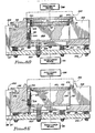
- FIGs. 1 to 8 depict apparatus for transporting a wafer to and from a pressure or polishing head.
- like reference characters herein and in European Patent Application No. 88302496.0 to Gill, Jr. also refer to corresponding elements. Consequently, the apparatus in Figs. 1 to 8 can be used to transport a wafer to and from a layer 120 in the pressure head of Fig. 2B of European Patent Application No. 88302496.0. Further, as illustrated in Fig. 1 of European Patent Application No.
- elongate carrier means 13 is provided to move the pressure head between a first operative position over the wafer transport apparatus of Figs. 1 to 8 herein and a second operative position over a polishing surface.
- the pressure head maintains the wafer against the polishing surface to polish the wafer.
- Fig. 1 illustrates a transport head assembly including a base 200, alignment cup 201, support piston 202, legs 203 to 205, and pins 206 to 208.
- Apertures 210 open at and extend downwardly from circular rim surface 211.
- Apertures 210 are generally formed at equal intervals around rim surface 211. Although only four apertures 210 are visible in Fig. 1, there actually six apertures 210 formed in rim surface 211.
- Three of the pins 206 to 208 and springs 209 are omitted from Fig. 1 for the sake of clarity.
- Each aperture 210 is, however, intended to be provided with a spring 209 and pin 206 to 208.
- Each pin 206 to 208 is identical in shape and dimension.
- Indents 212 to 214 each receive the upper arm 216 of a leg 203 to 205.
- the bottom arm 217 of each leg 203 to 205 is attached to base 200 with bolts 218.
- Legs 203 to 205 press alignment cup 201 against springs 219.
- the lower end of each spring 219 rests in a detent 220 formed in base 200.
- the upper end of each spring 219 rests in a similar detent (not visible) formed in cup 201.
- Support piston 202 is slidably received by cylindrical aperture 221 formed in cup 201.
- Springs 222 provide support for piston 202.
- the lower ends of springs 222 are received by detents 223.
- the upper ends of springs 222 are received by similar detents 224 formed in the bottom of piston 202.
- the upper tip 225 of each pin 206 to 208 is tapered in a truncated conical shape.
- Piston 202 includes cylindrical outer surfaces 226 which slidably contact surface 221. Arcuate lips or support surfaces 227 and 228 are above planer floor portions 229 and 230.
- the wafer storage cassette 232 shown in Fig. 6 includes a plurality of opposed, spaced apart pairs 223A, 223B and 234A, 234B of support ledges. Each ledge pair supports selected peripheral edge portions of a wafer 10.
- Wafer 10 includes spaced apart top 10A and bottom 10B surfaces. Surfaces 10A and 10B each terminate at edge 10C.
- the wafer dolly 236 is utilized to transport wafers from cassette 232 to the transport head assembly of Fig. 1.
- Dolly 236 includes rectangular base 237.
- Pin 238 is fixedly attached to base 237 and maintains roller 239 in position adjacent base 237.
- Elongate pin 240 is fixedly attached to base 237.
- Spring 241 is positioned around pin 240. Ends 242A and 242B of spring 241 bear against pin 243 fixedly attached to base 237. Spring 241 functions to bias dolly 236 so that roller 239 will travel along a track 244 (Fig. 3) in the manner described below.
- Tongue 245 of dolly 236 is connected to neck 246.
- Neck 246 is attached to base 237.
- Upper planer surface 248 of tongue 245 is bounded at either end by arcuate outwardly sloping or diverging surfaces 247 and 249. Surfaces 247 and 249 contact the lower linear circular portion 10D of edge 10C and prevent the bottom 10B of wafer 10 from contacting upper surface 248 of dolly 236.
- Fig. 4 The operation of the wafer dolly 236 of Fig. 4 is explained with reference to Fig. 3.
- the tongue 245, neck 246 and base 237 of dolly 236 are shown in ghost outline for the sake of clarity.
- roller 239 of dolly 236 moves along edge of track 244 of plate 262.
- Track 244 is, except for a jog 244A at the center of the track, linear. Jog 244A enables the orientation of tongue 245 to be altered by 180 degrees.
- the lower portion of pin 240 is pivotally connected to plate 250.
- Motive power means (not shown) are provided for moving plate 250 in directions 251 and 252 along cylindrical rod 253. Cylindrical aperture 254 in plate 250 slidably moves along rod 253.
- tongue 245 is in the orientation indicated by dashed lines 245.
- tongue 245, base 237, and neck 246 pivot 90° in the direction indicated by arrow 256. Consequently, base 237 assumes the orientation indicated by dashed lines 237A.
- dashed lines 259 generally indicate the position of a wafer cassette 232 and of means for raising and lowering cassette 232.
- dashed lines 260 generally indicate the location of the transport head assembly.
- Fig. 5 Operation of the wafer dolly 236 is further illustrated in Fig. 5.
- plate 250 moves in the direction of arrow 252 (Fig. 3) such that the base of dolly 236 arrives at the position indicated by dashed lines 237A
- the dolly 236 is in the position indicated in the right hand portion of Fig. 5 with tongue 245 extending into cassette 232 beneath a wafer 10.
- Means 260 is operated to lower cassette 232 while tongue 245 remains in fixed position.
- Lowering cassette 232 causes portions of the peripheral edge portion 10D to contact arcuate outwardly sloped surfaces 247 and 249 to lift wafer 10 off of ledge pair 233B (not visible in Fig. 5) and 233A.
- plate 250 is moved in the direction of arrow 251 to move roller 239 along edge 44 through jog 44A and to a point where base 237 is in the position indicated by dashed lines 237B in Fig. 3.
- dolly 236 is in the position indicated by the left hand portion of Fig. 5 with tongue 245 above the transport head assembly 264.
- assembly 264 is operated in the manner described in Figs. 8A to 8E to remove the wafer 10 from tongue 245 and position wafer 10 adjacent the pressure head.
- Fig. 8A the transport head assembly 264 and tongue 245 are in the position illustrated in the left hand portion of Fig. 5.
- Fig. 8B means 261 has been activated to upwardly displace base 200 and assembly 264 in the direction of arrow 270 while dolly 236 and tongue 245 remain stationary.
- portions of edge 10C of wafer 10 extend outwardly away from and free of contact with or support by tongue 245.
- transport assembly 264 is displaced in the direction of arrow 270 in Fig. 8B, selected points of these free portions contact the tapered upper ends 225 of the six spaced apart pins extending upwardly from surface 211. Tapered ends 225 guide wafer 10 downwardly intermediate the pins onto support surface 227.
- portions of walls 221, 226 and 263 move upwardly past tongue 245. Both the distance between parallel opposed walls 226 and 263 and the area circumscribed by wall 221 are sufficient to permit tongue 245 to fit therein when transport head assembly 264 rises in the direction of arrow 270.
- tongue 245 is shown separated from wafer 10 even though wafer 10 has not completely settled onto support surface 227. This is done for the sake of clarity. Normally wafer 10 will not be lifted and separated from stationary tongue 245 until wafer 10 is contacting support surface 227 and tongue 245 is beneath surface 227.
- the transport head assembly 264 rises when means 261 applies an upward force (acting in the direction of arrow 270) against base 200.
- a pneumatic cylinder, hydraulic cylinder or any other mechanical, electrical, manual etc. prior art means may be utilized to raise, and lower, base 200 and transport head assembly 264.
- Dolly 226 can remain in fixed position or can be removed from assembly 264 in the direction of arrow 252 (Fig. 3). In Figs. 8C to 8E, dolly 236 is assumed to have been removed from assembly 264.
- the positioning means 266 can comprise the counterbalanced apparatus of Fig. 1 of European Patent Application 88302496.0 or can comprise any other appropriate prior art positioning apparatus.
- Fig. 8E illustrates the position of piston 202 and springs 219, 222 after means 261 have been utilized to upwardly displace base 200 to cause piston 202 to move upwardly and press wafer 10 against layer 120. Once wafer 10 is pressed against layer 120.
- means 266 can be utilized to lift pressure head 265 up away from the transport head assembly and means 261 can be utilized to lower the transport head assembly back to the position of Fig. 8A. Means 266 is then utilized to move pressure head 265 to a polishing station to polish wafer 10. After the wafer 10 is polished to within selected tolerances, pressure head 265 is positioned over the water track illustrated in Figs. 2 and 7.
- the water track of Figs. 2 and 7 includes an elongate rectangular housing 271 having a circular reservoir formed therein to receive a wafer ejected from pressure head 265.
- the wafer 10 is separated from layer 120 by discontinuing the suction through apertures 90 and by directing water flow outwardly through apertures 90.
- the circular reservoir in housing 271 has a floor 274 and upwardly extending outwardly sloped circular walls 273 and 275.
- Vertically oriented cylindrical wall 293 interconnects walls 273 and 275.
- An elongate channel having a floor 76 is in fluid communication with the circular reservoir.
- Floors 274 and 276 are co-planar.
- the elongate channel includes a pair of elongate, opposed spaced apart sloped side wafer-guide surfaces 277 and 278 extending upwardly and outwardly away from floor 276. Each sloped wafer-guide surface 278, 279 terminates at a vertical side wall 280 and 279, respectively.
- a liquid or a mixture of a liquid and gas flows into the circular reservoir and elongate channel in the direction of arrows 281 through orifice 282. Since orifice 282 injects fluid 281 to the side of the center of a wafer in the reservoir, the flow 281 of fluid imparts a rotational force on the wafer, causing it to rotate as it travels from the reservoir down the elongate channel.
- Gas can be included in the fluid flowing from orifice 282, or can be bubbled through apertures formed in floors 274 and 276.
- the admixture of gas to fluid flowing through the reservoir and channel facilitates the travel of a wafer 10 down the water track because the air bubbles function like ball bearings intermediate wafer 10 and floors 274 and 276.
- the lower linear circular portion 10D of edge 10C contacts sloped wall 273 while the wafer is in the circular reservoir and contacts sloped, parallel opposed walls 277 and 278 while the wafer travels down the elongate channel. Accordingly, wall 273 is sized and walls 277, 278 are spaced apart such that the bottom 10B of wafer 10 does not contact floors 174, 176 while moving down the water track.
- the level of water in the track is ordinarily sufficient to keep a wafer 10 in the track covered, or at least coated, with water.
- sloped ceiling 286 of member 287 gradually constricts the size of the channel through which water in the track can flow, tending to increase the velocity of water moving through the channel and facilitating movement of the wafer out of the dispensing end 285 into a cassette 232 positioned adjacent end 275.
- a stream of water directed through orifice 288 in the direction of arrow 289 flows against a wafer 10 moving through the channel toward dispensing end 285.
- the water imparts a downward force against the wafer 10 and also imparts a force in the direction of travel of wafer 10 which assists movement of the wafer 10 along the channel and out of end 185.
- the downward force produced by fluid flowing through orifice 288 is important because it prevents wafer 10 from tipping or tilting after it leaves end 285 and before the wafer 10 has moved completely into its storage slot 233A, 233B in cassette 232.
- Water or other fluid flowing out of the dispensing end 285 of the water track is collected in a reservoir 290. Water from the reservoir 290 can be recycled by pump means 291 back to orifices 282, 283, 284. After a wafer I0 travels down the water track and out of dispensing end 285 into a storage slot 233A, 233B in cassette 232, means 260 lowers (or raises) cassette 232 to position another storage slot to receive a wafer 10 from the water track. When the cassette is filled, as would be the cassette in Fig. 6 after is receives a wafer 10 in slot 233A, 233B, the cassette is removed and an empty cassette installed in the reservoir.
Landscapes
- Engineering & Computer Science (AREA)
- Mechanical Engineering (AREA)
- Mechanical Treatment Of Semiconductor (AREA)
- Finish Polishing, Edge Sharpening, And Grinding By Specific Grinding Devices (AREA)
- Container, Conveyance, Adherence, Positioning, Of Wafer (AREA)
- Constituent Portions Of Griding Lathes, Driving, Sensing And Control (AREA)
Abstract
Description
- This invention relates to polishing apparatus.
- More particularly, the invention relates to apparatus for polishing a side of a thin, flat wafer of a semiconductor material, the apparatus including a polishing head which receives the wafer at a wafer load station, which carries the wafer to a wetted polishing surface under pressure, and which rotates and oscillates the wafer over the polishing surface.
- In a further respect, the invention relates to apparatus of the type described which includes apparatus for transporting a wafer to the load station for pickup by the polishing head while preventing dust particles and other impurities from contacting the wafer during its transport to the load station.
- Apparatus for polishing thin, flat semiconductor wafers is well known in the art. See, for example, U. S. Patent Nos. 3,841,031 to Walsh and 4,193,226 to Gill, Jr. et al. and the published European Patent Application No. 88302496.0 to Gill, Jr. Such apparatus includes a polishing head which receives a wafer at a wafer load station and carries the wafer to a wetted polishing station. The polishing head presses the wafer downwardly against the wetted polishing surface. The polishing head can rotate and oscillate the wafer over the polishing surface. A particular problem encountered in transporting the wafer to the load station for pickup by the polishing head is preventing contaminants from contacting the wafer.
- Accordingly, it would be highly desirable to provide improved semiconductor polishing apparatus of the general type described which would permit the ready transportation of a wafer to a wafer load station for pickup by the polishing head and which would prevent contaminants from contacting the wafer during its transport to the load station.
- Therefore, it is a principal object of the invention to provide improved apparatus for polishing a surface of a flat semiconductor wafer.
- These and other, further and more specific objects and advantages of the invention will be apparent to those skilled in the art from the following detailed description thereof, taken in conjunction with the drawings, in which:
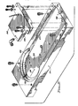
- Fig. 1 is an exploded assembly view of a wafer transport head assembly utilized to remove a wafer from a dolly and transport the wafer to the polishing head;
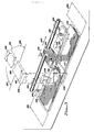
- Fig. 2 is an exploded assembly view of a wafer water track assembly utilized to carry a polished wafer from the polishing head to a storage cassette;
- Fig. 3 is an assembly view of a wafer dolly and track utilized to transfer a wafer from a wafer cassette to the wafer transport head assembly;
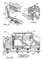
- Fig. 4. is a perspective view of the wafer transport dolly;
- Fig. 5 is an elevation view illustrating use of the wafer dolly to transport a wafer from a wafer cassette to the wafer transport head assembly;
- Fig. 6 is a perspective view of a wafer cassette;
- Fig. 7 is a section view illustrating operation of the wafer water track assembly to transport a wafer from the polishing head to a wafer cassette; and,
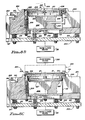
- Figs. 8A to 8E illustrate operation of the wafer transport head assembly to remove a wafer from the wafer dolly and position the wafer adjacent the polishing head.
- Briefly, in accordance with our invention, we provide apparatus for transporting a wafer into position against the pressure head of apparatus for polishing the wafer. The transport apparatus includes a dolly for positioning a wafer over a transport head assembly. The transport head assembly removes the wafer from the dolly and positions the wafer against the pressure head. When the transport head assembly removes the wafer from the dolly and positions the wafer against the pressure head, the transport head assembly only contacts the wafer at selected points at the periphery of the wafer.
- Turning now to the drawings, which depict the presently preferred embodiments of the invention for the purpose of illustrating the practice thereof and not by way of limitation of the scope of the invention, and in which like reference characters refer to corresponding elements throughout the several views, Figs. 1 to 8 depict apparatus for transporting a wafer to and from a pressure or polishing head. In order to facilitate the understanding of the invention, like reference characters herein and in European Patent Application No. 88302496.0 to Gill, Jr. also refer to corresponding elements. Consequently, the apparatus in Figs. 1 to 8 can be used to transport a wafer to and from a
layer 120 in the pressure head of Fig. 2B of European Patent Application No. 88302496.0. Further, as illustrated in Fig. 1 of European Patent Application No. 88301496.0, and as is well known in the art, elongate carrier means 13 is provided to move the pressure head between a first operative position over the wafer transport apparatus of Figs. 1 to 8 herein and a second operative position over a polishing surface. The pressure head maintains the wafer against the polishing surface to polish the wafer. - Fig. 1 illustrates a transport head assembly including a
base 200,alignment cup 201,support piston 202,legs 203 to 205, andpins 206 to 208.Apertures 210 open at and extend downwardly fromcircular rim surface 211.Apertures 210 are generally formed at equal intervals aroundrim surface 211. Although only fourapertures 210 are visible in Fig. 1, there actually sixapertures 210 formed inrim surface 211. Three of thepins 206 to 208 andsprings 209 are omitted from Fig. 1 for the sake of clarity. Eachaperture 210 is, however, intended to be provided with aspring 209 andpin 206 to 208. Eachpin 206 to 208 is identical in shape and dimension. Indents 212 to 214 each receive theupper arm 216 of aleg 203 to 205. Thebottom arm 217 of eachleg 203 to 205 is attached tobase 200 withbolts 218. Legs 203 to 205press alignment cup 201 againstsprings 219. The lower end of eachspring 219 rests in a detent 220 formed inbase 200. The upper end of eachspring 219 rests in a similar detent (not visible) formed incup 201.Support piston 202 is slidably received bycylindrical aperture 221 formed incup 201. Springs 222 provide support forpiston 202. The lower ends ofsprings 222 are received bydetents 223. The upper ends ofsprings 222 are received bysimilar detents 224 formed in the bottom ofpiston 202. Theupper tip 225 of eachpin 206 to 208 is tapered in a truncated conical shape. - Piston 202 includes cylindrical
outer surfaces 226 which slidably contactsurface 221. Arcuate lips orsupport surfaces planer floor portions 229 and 230. - The
wafer storage cassette 232 shown in Fig. 6 includes a plurality of opposed, spaced apartpairs 223A, 223B and 234A, 234B of support ledges. Each ledge pair supports selected peripheral edge portions of awafer 10. Wafer 10 includes spaced apart top 10A and bottom 10B surfaces. Surfaces 10A and 10B each terminate at edge 10C. - The
wafer dolly 236 is utilized to transport wafers fromcassette 232 to the transport head assembly of Fig. 1. Dolly 236 includesrectangular base 237.Pin 238 is fixedly attached tobase 237 and maintainsroller 239 in positionadjacent base 237. Elongatepin 240 is fixedly attached tobase 237. Spring 241 is positioned aroundpin 240. Ends 242A and 242B of spring 241 bear againstpin 243 fixedly attached tobase 237. Spring 241 functions to bias dolly 236 so thatroller 239 will travel along a track 244 (Fig. 3) in the manner described below.Tongue 245 ofdolly 236 is connected toneck 246. Neck 246 is attached tobase 237.Upper planer surface 248 oftongue 245 is bounded at either end by arcuate outwardly sloping or divergingsurfaces Surfaces wafer 10 from contactingupper surface 248 ofdolly 236. - The operation of the
wafer dolly 236 of Fig. 4 is explained with reference to Fig. 3. In Fig. 3, thetongue 245,neck 246 andbase 237 ofdolly 236 are shown in ghost outline for the sake of clarity. During operation,roller 239 ofdolly 236 moves along edge oftrack 244 ofplate 262.Track 244 is, except for a jog 244A at the center of the track, linear. Jog 244A enables the orientation oftongue 245 to be altered by 180 degrees. The lower portion ofpin 240 is pivotally connected toplate 250. Motive power means (not shown) are provided for movingplate 250 indirections cylindrical rod 253.Cylindrical aperture 254 inplate 250 slidably moves alongrod 253. Whenplate 250 is at the midpoint illustrated in Fig. 3,tongue 245 is in the orientation indicated by dashedlines 245. Whenplate 250 is moved in the direction ofarrow 252,tongue 245,base 237, andneck 246 pivot 90° in the direction indicated byarrow 256. Consequently,base 237 assumes the orientation indicated by dashedlines 237A. Conversely, ifplate 250 moves from the center position illustrated in Fig. 3 in the direction ofarrow 251, thetongue 245,neck 246, andbase 237 are rotated 90° in the direction ofarrow 257 andbase 237 assumes the orientation illustrated by dashed lines 237B. In Fig. 3, dashed lines 259 generally indicate the position of awafer cassette 232 and of means for raising and loweringcassette 232. Dashedlines 260 generally indicate the location of the transport head assembly. - Operation of the
wafer dolly 236 is further illustrated in Fig. 5. Whenplate 250 moves in the direction of arrow 252 (Fig. 3) such that the base ofdolly 236 arrives at the position indicated by dashedlines 237A, thedolly 236 is in the position indicated in the right hand portion of Fig. 5 withtongue 245 extending intocassette 232 beneath awafer 10.Means 260 is operated tolower cassette 232 whiletongue 245 remains in fixed position. Loweringcassette 232 causes portions of the peripheral edge portion 10D to contact arcuate outwardlysloped surfaces wafer 10 off of ledge pair 233B (not visible in Fig. 5) and 233A. Afterwafer 10 is so positioned onsurfaces plate 250 is moved in the direction ofarrow 251 to moveroller 239 along edge 44 through jog 44A and to a point wherebase 237 is in the position indicated by dashed lines 237B in Fig. 3. When the base is in the position indicated by dashed lines 237B,dolly 236 is in the position indicated by the left hand portion of Fig. 5 withtongue 245 above thetransport head assembly 264. Oncetongue 245 is positioned overtransport head assembly 264,assembly 264 is operated in the manner described in Figs. 8A to 8E to remove thewafer 10 fromtongue 245 andposition wafer 10 adjacent the pressure head. - In Fig. 8A, the
transport head assembly 264 andtongue 245 are in the position illustrated in the left hand portion of Fig. 5. - In Fig. 8B, means 261 has been activated to upwardly displace base 200 and
assembly 264 in the direction ofarrow 270 whiledolly 236 andtongue 245 remain stationary. As shown in Fig. 4, portions of edge 10C ofwafer 10 extend outwardly away from and free of contact with or support bytongue 245. Whentransport assembly 264 is displaced in the direction ofarrow 270 in Fig. 8B, selected points of these free portions contact the tapered upper ends 225 of the six spaced apart pins extending upwardly fromsurface 211. Tapered ends 225guide wafer 10 downwardly intermediate the pins ontosupport surface 227. Whiletransport head assembly 264 rises in Fig. 8B, portions ofwalls past tongue 245. Both the distance between parallelopposed walls wall 221 are sufficient to permittongue 245 to fit therein whentransport head assembly 264 rises in the direction ofarrow 270. - In Fig. 8B,
tongue 245 is shown separated fromwafer 10 even thoughwafer 10 has not completely settled ontosupport surface 227. This is done for the sake of clarity. Normallywafer 10 will not be lifted and separated fromstationary tongue 245 untilwafer 10 is contactingsupport surface 227 andtongue 245 is beneathsurface 227. - The
transport head assembly 264 rises when means 261 applies an upward force (acting in the direction of arrow 270) againstbase 200. A pneumatic cylinder, hydraulic cylinder or any other mechanical, electrical, manual etc. prior art means may be utilized to raise, and lower,base 200 andtransport head assembly 264. - After
wafer 10 is resting on circularplaner support surface 227, thepressure head 265 is lowered to a positionadjacent alignment cup 201.Dolly 226 can remain in fixed position or can be removed fromassembly 264 in the direction of arrow 252 (Fig. 3). In Figs. 8C to 8E,dolly 236 is assumed to have been removed fromassembly 264. - After
wafer 10 has settled ontosupport surface 227, the upward movement oftransport head assembly 264 is halted andpressure head 265 is positionedadjacent alignment cup 201 in the manner illustrated in Fig. 8C.Means 266 are used to positionpressure head 265 overalignment cup 201. The positioning means 266 can comprise the counterbalanced apparatus of Fig. 1 of European Patent Application 88302496.0 or can comprise any other appropriate prior art positioning apparatus. - When
pressure head 265 is positionedadjacent alignment cup 201 as illustrated in Fig. 8C, water is squirted through apertures (see apertures 90 in Fig. 2B of European Patent Application 88302496.0) formed in polishinghead 265 towet wafer 10. The flow of water through the apertures is then discontinued and a suction is applied to the apertures. Whilepressure head 265 is maintained in a fixed position, means 261 is utilized to resume the movement ofbase 200 andtransport head assembly 264 in the direction ofarrow 270. Astransport head assembly 264 continues to rise, the bottomcircular planer surface 272 oflip 72A contacts the six pins (includingpins 206 to 208) inapertures 210.Surface 272 downwardly forces the six pins intoapertures 210, compressing springs 209. The upward movement ofalignment cup 201 halts when the lowercircular planer surface 272 oflip 72A is contacted bycircular surface 211 in the manner illustrated in Fig. 8D. Aftersurface 211 contacts surface 272, means 261 is utilized to continue to upwardly displace base 200, compressingsprings springs 219 are being compressed,pressure head 265 is maintained in fixed position, which causesalignment cup 201 to also remain in fixed position. Consequently, whilebase 200 continues to move upwardly and whilealignment cup 201 remains stationary whilesprings 219 are further compressed, the continued compression ofsprings 222 causespiston 202 to be upwardly displaced in the direction ofarrow 270 to presswafer 10 againstlayer 120. Oncewafer 10 is positioned bypiston 202 immediately adjacent or contactinglayer 120, the suction through apertures 90 maintains the wafer againstlayer 120. Fig. 8E illustrates the position ofpiston 202 and springs 219, 222 aftermeans 261 have been utilized to upwardly displace base 200 to causepiston 202 to move upwardly andpress wafer 10 againstlayer 120. Oncewafer 10 is pressed againstlayer 120. means 266 can be utilized to liftpressure head 265 up away from the transport head assembly and means 261 can be utilized to lower the transport head assembly back to the position of Fig. 8A.Means 266 is then utilized to movepressure head 265 to a polishing station to polishwafer 10. After thewafer 10 is polished to within selected tolerances,pressure head 265 is positioned over the water track illustrated in Figs. 2 and 7. - The water track of Figs. 2 and 7 includes an elongate
rectangular housing 271 having a circular reservoir formed therein to receive a wafer ejected frompressure head 265. Thewafer 10 is separated fromlayer 120 by discontinuing the suction through apertures 90 and by directing water flow outwardly through apertures 90. The circular reservoir inhousing 271 has afloor 274 and upwardly extending outwardly slopedcircular walls cylindrical wall 293interconnects walls Floors guide surfaces floor 276. Each sloped wafer-guide surface vertical side wall arrows 281 throughorifice 282. Sinceorifice 282 injects fluid 281 to the side of the center of a wafer in the reservoir, theflow 281 of fluid imparts a rotational force on the wafer, causing it to rotate as it travels from the reservoir down the elongate channel. Gas can be included in the fluid flowing fromorifice 282, or can be bubbled through apertures formed infloors wafer 10 down the water track because the air bubbles function like ball bearingsintermediate wafer 10 andfloors wall 273 while the wafer is in the circular reservoir and contacts sloped, parallelopposed walls wall 273 is sized andwalls wafer 10 does not contact floors 174, 176 while moving down the water track. The level of water in the track is ordinarily sufficient to keep awafer 10 in the track covered, or at least coated, with water. - When a wafer moving along the water track approaches the dispensing
end 285 of the elongate channel, slopedceiling 286 ofmember 287 gradually constricts the size of the channel through which water in the track can flow, tending to increase the velocity of water moving through the channel and facilitating movement of the wafer out of the dispensingend 285 into acassette 232 positionedadjacent end 275. A stream of water directed throughorifice 288 in the direction ofarrow 289 flows against awafer 10 moving through the channel toward dispensingend 285. The water imparts a downward force against thewafer 10 and also imparts a force in the direction of travel ofwafer 10 which assists movement of thewafer 10 along the channel and out of end 185. The downward force produced by fluid flowing throughorifice 288 is important because it preventswafer 10 from tipping or tilting after it leavesend 285 and before thewafer 10 has moved completely into itsstorage slot 233A, 233B incassette 232. - Water or other fluid flowing out of the dispensing
end 285 of the water track is collected in areservoir 290. Water from thereservoir 290 can be recycled by pump means 291 back toorifices end 285 into astorage slot 233A, 233B incassette 232, means 260 lowers (or raises)cassette 232 to position another storage slot to receive awafer 10 from the water track. When the cassette is filled, as would be the cassette in Fig. 6 after is receives awafer 10 inslot 233A, 233B, the cassette is removed and an empty cassette installed in the reservoir. - Having described my invention in such terms as to enable those skilled in the art to understand and practise it, and having identified the presently preferred embodiments thereof, I Claim:
Claims (3)
a peripheral edge circumscribing said wafer, and
spaced apart top and bottom surfaces each terminating at said edge,
said polishing apparatus including
at least one station having a polishing surface,
a frame, and
elongate carrier means mounted on said frame to move said pressure head between at least two operative positions,
a first operative position with said head positioned over said transport apparatus, and
a second operative position with said head positioned over said station,
said pressure head including a lower portion for maintaining the wafer in contact therewith and against said polishing surface when said pressure head is positioned over said station,
said transport apparatus including
(i) a base,
(ii) an alignment cup having a support surface shaped and dimensioned to receive and support said selected peripheral edge portions of said wafer to support said wafer in a selected orientation, and
a wall structure defining a central opening formed in said alignment cup intermediate and extending downwardly from said support surface and shaped and dimensioned to receive said tongue, and
(iii) a plurality of spaced apart upstanding pins for contacting said selected peripheral areas of said wafer to guide said wafer when said wafer slides intermediate said pins downwardly toward said support surface, said pins circumscribing said central opening an said support surface;
said central opening, support surface and pins being shaped and dimensioned such that when said tongue is in said selected operative position over said transport head assembly and said displacement means upwardly displaces said transport head assembly toward said tongue, said wafer slides intermediate said pins onto said support surface while said wall structure and support surface move upwardly past said tongue; and,
(iv) means for upwardly displacing said support area to position said wafer adjacent said lower portion of said pressure head when said pressure head is in said first operative position.
a peripheral edge circumscribing said wafer, and
spaced apart top and bottom surfaces each terminating at said edge,
said polishing apparatus including
at least one station having a polishing surface,
a frame, and
elongate carrier means mounted on said frame to move said pressure head between at least two operative positions,
a first operative position with said head positioned over said transport apparatus, and
a second operative position with said head positioned over said station,
said pressure head including a lower portion for maintaining the wafer in contact therewith and against said polishing surface when said pressure head is positioned over said station,
said fluid housing apparatus including
(i) a floor, and
(ii) sloped side surfaced extending upwardly away from said floor to receive and contact at least selected portions of said peripheral edge of said wafer to prevent said bottom surface from contacting said floor of said reservoir;
(i) a floor,
(ii) elongate, opposed, spaced apart sloped side surfaces extending upwardly away from said floor of said channel to receive and contact portions of said peripheral edge of said wafer to prevent said bottom surface from contacting said floor of said channel when said wafer moves along said channel, and
(iii) a wafer-dispensing end;
Applications Claiming Priority (2)
| Application Number | Priority Date | Filing Date | Title |
|---|---|---|---|
| US208685 | 1988-06-20 | ||
| US07/208,685 US4944119A (en) | 1988-06-20 | 1988-06-20 | Apparatus for transporting wafer to and from polishing head |
Related Child Applications (2)
| Application Number | Title | Priority Date | Filing Date |
|---|---|---|---|
| EP91113965A Division EP0464864A3 (en) | 1988-06-20 | 1989-06-13 | Apparatus for transporting a wafer |
| EP91113965.7 Division-Into | 1989-06-13 |
Publications (3)
| Publication Number | Publication Date |
|---|---|
| EP0347718A2 true EP0347718A2 (en) | 1989-12-27 |
| EP0347718A3 EP0347718A3 (en) | 1991-01-02 |
| EP0347718B1 EP0347718B1 (en) | 1995-03-22 |
Family
ID=22775586
Family Applications (2)
| Application Number | Title | Priority Date | Filing Date |
|---|---|---|---|
| EP91113965A Withdrawn EP0464864A3 (en) | 1988-06-20 | 1989-06-13 | Apparatus for transporting a wafer |
| EP89110665A Expired - Lifetime EP0347718B1 (en) | 1988-06-20 | 1989-06-13 | Apparatus for transporting wafer to and from polishing head |
Family Applications Before (1)
| Application Number | Title | Priority Date | Filing Date |
|---|---|---|---|
| EP91113965A Withdrawn EP0464864A3 (en) | 1988-06-20 | 1989-06-13 | Apparatus for transporting a wafer |
Country Status (4)
| Country | Link |
|---|---|
| US (1) | US4944119A (en) |
| EP (2) | EP0464864A3 (en) |
| JP (1) | JP2683279B2 (en) |
| DE (1) | DE68921793T2 (en) |
Cited By (4)
| Publication number | Priority date | Publication date | Assignee | Title |
|---|---|---|---|---|
| EP1061558A2 (en) * | 1999-06-14 | 2000-12-20 | Applied Materials, Inc. | Edge contact loadcup |
| US7044832B2 (en) | 2003-11-17 | 2006-05-16 | Applied Materials | Load cup for chemical mechanical polishing |
| US7101253B2 (en) | 2002-08-27 | 2006-09-05 | Applied Materials Inc. | Load cup for chemical mechanical polishing |
| EP1707314A1 (en) * | 2005-04-01 | 2006-10-04 | Fujikoshi Machinery Corporation | Polishing apparatus |
Families Citing this family (42)
| Publication number | Priority date | Publication date | Assignee | Title |
|---|---|---|---|---|
| US5095661A (en) * | 1988-06-20 | 1992-03-17 | Westech Systems, Inc. | Apparatus for transporting wafer to and from polishing head |
| US5018938A (en) * | 1990-05-18 | 1991-05-28 | At&T Bell Laboratories | Method and apparatus for separating chips |
| US5193316A (en) * | 1991-10-29 | 1993-03-16 | Texas Instruments Incorporated | Semiconductor wafer polishing using a hydrostatic medium |
| US5329732A (en) * | 1992-06-15 | 1994-07-19 | Speedfam Corporation | Wafer polishing method and apparatus |
| USRE38878E1 (en) * | 1992-09-24 | 2005-11-15 | Ebara Corporation | Polishing apparatus |
| DE69325756T2 (en) * | 1992-09-24 | 2000-03-02 | Ebara Corp | Polisher |
| US5733175A (en) | 1994-04-25 | 1998-03-31 | Leach; Michael A. | Polishing a workpiece using equal velocity at all points overlapping a polisher |
| US5607341A (en) | 1994-08-08 | 1997-03-04 | Leach; Michael A. | Method and structure for polishing a wafer during manufacture of integrated circuits |
| US6024630A (en) | 1995-06-09 | 2000-02-15 | Applied Materials, Inc. | Fluid-pressure regulated wafer polishing head |
| US5681215A (en) * | 1995-10-27 | 1997-10-28 | Applied Materials, Inc. | Carrier head design for a chemical mechanical polishing apparatus |
| KR100487590B1 (en) | 1995-08-21 | 2005-08-04 | 가부시키가이샤 에바라 세이사꾸쇼 | Polishing device |
| US5738574A (en) * | 1995-10-27 | 1998-04-14 | Applied Materials, Inc. | Continuous processing system for chemical mechanical polishing |
| US5804507A (en) * | 1995-10-27 | 1998-09-08 | Applied Materials, Inc. | Radially oscillating carousel processing system for chemical mechanical polishing |
| US7097544B1 (en) * | 1995-10-27 | 2006-08-29 | Applied Materials Inc. | Chemical mechanical polishing system having multiple polishing stations and providing relative linear polishing motion |
| US5762544A (en) * | 1995-10-27 | 1998-06-09 | Applied Materials, Inc. | Carrier head design for a chemical mechanical polishing apparatus |
| US5762543A (en) * | 1995-11-30 | 1998-06-09 | Speedfam Corporation | Polishing apparatus with improved product unloading |
| JP3580936B2 (en) * | 1996-02-26 | 2004-10-27 | 株式会社荏原製作所 | Polisher pusher and polishing device |
| US6050884A (en) * | 1996-02-28 | 2000-04-18 | Ebara Corporation | Polishing apparatus |
| US6425812B1 (en) | 1997-04-08 | 2002-07-30 | Lam Research Corporation | Polishing head for chemical mechanical polishing using linear planarization technology |
| US6244946B1 (en) | 1997-04-08 | 2001-06-12 | Lam Research Corporation | Polishing head with removable subcarrier |
| US5893795A (en) * | 1997-07-11 | 1999-04-13 | Applied Materials, Inc. | Apparatus for moving a cassette |
| US5865670A (en) * | 1997-09-30 | 1999-02-02 | Memc Electronic Materials, Inc. | Wafer demount apparatus |
| EP0911114B1 (en) | 1997-10-20 | 2007-08-01 | Ebara Corporation | Polishing apparatus |
| US6884721B2 (en) * | 1997-12-25 | 2005-04-26 | Shin-Etsu Handotai Co., Ltd. | Silicon wafer storage water and silicon wafer storage method |
| US5954888A (en) * | 1998-02-09 | 1999-09-21 | Speedfam Corporation | Post-CMP wet-HF cleaning station |
| US6010392A (en) * | 1998-02-17 | 2000-01-04 | International Business Machines Corporation | Die thinning apparatus |
| US5944588A (en) * | 1998-06-25 | 1999-08-31 | International Business Machines Corporation | Chemical mechanical polisher |
| US6159083A (en) * | 1998-07-15 | 2000-12-12 | Aplex, Inc. | Polishing head for a chemical mechanical polishing apparatus |
| US6074285A (en) * | 1998-08-06 | 2000-06-13 | National Science Council | Reciprocating friction drive-type ultra precision machine |
| US7425250B2 (en) * | 1998-12-01 | 2008-09-16 | Novellus Systems, Inc. | Electrochemical mechanical processing apparatus |
| US6464571B2 (en) * | 1998-12-01 | 2002-10-15 | Nutool, Inc. | Polishing apparatus and method with belt drive system adapted to extend the lifetime of a refreshing polishing belt provided therein |
| US6409585B1 (en) | 1998-12-21 | 2002-06-25 | Ebara Corporation | Polishing apparatus and holder for holding an article to be polished |
| US6066030A (en) * | 1999-03-04 | 2000-05-23 | International Business Machines Corporation | Electroetch and chemical mechanical polishing equipment |
| US6666756B1 (en) | 2000-03-31 | 2003-12-23 | Lam Research Corporation | Wafer carrier head assembly |
| US6358126B1 (en) | 2000-05-23 | 2002-03-19 | Ebara Corporation | Polishing apparatus |
| US6398631B1 (en) | 2001-02-02 | 2002-06-04 | Memc Electronic Materials, Inc. | Method and apparatus to place wafers into and out of machine |
| US7648622B2 (en) * | 2004-02-27 | 2010-01-19 | Novellus Systems, Inc. | System and method for electrochemical mechanical polishing |
| KR102591914B1 (en) * | 2016-11-25 | 2023-10-23 | 주식회사 케이씨텍 | Apparatus of loading substrate in chemical mechanical polishing system |
| CN107671713A (en) * | 2017-11-16 | 2018-02-09 | 无锡海特精密模具有限公司 | A kind of lapping device |
| CN108527117A (en) * | 2018-04-08 | 2018-09-14 | 乐康 | A kind of novel automatic buffing equipment |
| CN108527116A (en) * | 2018-04-08 | 2018-09-14 | 乐康 | A kind of automatic buffing equipment |
| US11705354B2 (en) | 2020-07-10 | 2023-07-18 | Applied Materials, Inc. | Substrate handling systems |
Citations (3)
| Publication number | Priority date | Publication date | Assignee | Title |
|---|---|---|---|---|
| US3841031A (en) * | 1970-10-21 | 1974-10-15 | Monsanto Co | Process for polishing thin elements |
| US4193226A (en) * | 1977-09-21 | 1980-03-18 | Kayex Corporation | Polishing apparatus |
| EP0284343A2 (en) * | 1987-03-23 | 1988-09-28 | Westech Systems, Inc. | Polishing apparatus |
Family Cites Families (1)
| Publication number | Priority date | Publication date | Assignee | Title |
|---|---|---|---|---|
| DE3514741A1 (en) * | 1985-04-24 | 1986-10-30 | Supfina Maschinenfabrik Hentzen Kg, 5630 Remscheid | DEVICE FOR FINISHING LEVEL SURFACES OF DISK-SHAPED WORKPIECES WITH UNPROCESSED SUPPORT PAGE AND LOW WALL THICKNESS |
-
1988
- 1988-06-20 US US07/208,685 patent/US4944119A/en not_active Expired - Fee Related
-
1989
- 1989-06-13 DE DE68921793T patent/DE68921793T2/en not_active Expired - Fee Related
- 1989-06-13 EP EP91113965A patent/EP0464864A3/en not_active Withdrawn
- 1989-06-13 EP EP89110665A patent/EP0347718B1/en not_active Expired - Lifetime
- 1989-06-20 JP JP15813289A patent/JP2683279B2/en not_active Expired - Lifetime
Patent Citations (3)
| Publication number | Priority date | Publication date | Assignee | Title |
|---|---|---|---|---|
| US3841031A (en) * | 1970-10-21 | 1974-10-15 | Monsanto Co | Process for polishing thin elements |
| US4193226A (en) * | 1977-09-21 | 1980-03-18 | Kayex Corporation | Polishing apparatus |
| EP0284343A2 (en) * | 1987-03-23 | 1988-09-28 | Westech Systems, Inc. | Polishing apparatus |
Cited By (7)
| Publication number | Priority date | Publication date | Assignee | Title |
|---|---|---|---|---|
| EP1061558A2 (en) * | 1999-06-14 | 2000-12-20 | Applied Materials, Inc. | Edge contact loadcup |
| EP1061558A3 (en) * | 1999-06-14 | 2001-08-16 | Applied Materials, Inc. | Edge contact loadcup |
| US6716086B1 (en) | 1999-06-14 | 2004-04-06 | Applied Materials Inc. | Edge contact loadcup |
| US7101253B2 (en) | 2002-08-27 | 2006-09-05 | Applied Materials Inc. | Load cup for chemical mechanical polishing |
| US7044832B2 (en) | 2003-11-17 | 2006-05-16 | Applied Materials | Load cup for chemical mechanical polishing |
| EP1707314A1 (en) * | 2005-04-01 | 2006-10-04 | Fujikoshi Machinery Corporation | Polishing apparatus |
| US7235001B2 (en) | 2005-04-01 | 2007-06-26 | Fujikoshi Machinery Corp. | Polishing apparatus |
Also Published As
| Publication number | Publication date |
|---|---|
| EP0347718B1 (en) | 1995-03-22 |
| DE68921793T2 (en) | 1995-07-13 |
| JP2683279B2 (en) | 1997-11-26 |
| EP0464864A2 (en) | 1992-01-08 |
| EP0464864A3 (en) | 1994-12-21 |
| JPH0248170A (en) | 1990-02-16 |
| EP0347718A3 (en) | 1991-01-02 |
| US4944119A (en) | 1990-07-31 |
| DE68921793D1 (en) | 1995-04-27 |
Similar Documents
| Publication | Publication Date | Title |
|---|---|---|
| EP0347718B1 (en) | Apparatus for transporting wafer to and from polishing head | |
| US5095661A (en) | Apparatus for transporting wafer to and from polishing head | |
| US5562524A (en) | Polishing apparatus | |
| EP0577762B1 (en) | Cleaning brush for semiconductor wafer | |
| US5649854A (en) | Polishing apparatus with indexing wafer processing stations | |
| US6390901B1 (en) | Polishing apparatus | |
| US5226758A (en) | Method and an apparatus for handling wafers | |
| KR970067676A (en) | Polishing device | |
| KR20110010391A (en) | Substrate polishing apparatus and method of polishing substrate using the same | |
| JPH1080856A (en) | Flattening device and using method thereof | |
| US20010039175A1 (en) | Polishing pad surface on hollow posts | |
| US6805616B2 (en) | Wafer planarization apparatus and planarization method thereof | |
| JP2002079461A (en) | Polishing device | |
| US6685543B2 (en) | Compensating chemical mechanical wafer polishing apparatus and method | |
| CA2213847A1 (en) | Maintenance strut for dock leveler | |
| US6447381B1 (en) | Polishing apparatus | |
| WO2003037567A1 (en) | Polishing apparatus | |
| US6306022B1 (en) | Chemical-mechanical polishing device | |
| US20030143937A1 (en) | Contamination prevention system and method | |
| CN218658362U (en) | Wooden panel burnishing machine | |
| KR20110018715A (en) | Substrate polishing apparatus and method of polishing substrate using the same | |
| CN111604791A (en) | Regenerated wafer semiconductor processing device | |
| CN211310732U (en) | Lifting device for building facade transformation | |
| KR950010440Y1 (en) | Wafer transper device | |
| JPH11204470A (en) | Inclined work dipping method and device |
Legal Events
| Date | Code | Title | Description |
|---|---|---|---|
| PUAI | Public reference made under article 153(3) epc to a published international application that has entered the european phase |
Free format text: ORIGINAL CODE: 0009012 |
|
| AK | Designated contracting states |
Kind code of ref document: A2 Designated state(s): CH DE FR GB IT LI |
|
| PUAL | Search report despatched |
Free format text: ORIGINAL CODE: 0009013 |
|
| AK | Designated contracting states |
Kind code of ref document: A3 Designated state(s): CH DE FR GB IT LI |
|
| 17P | Request for examination filed |
Effective date: 19910628 |
|
| 17Q | First examination report despatched |
Effective date: 19930422 |
|
| GRAA | (expected) grant |
Free format text: ORIGINAL CODE: 0009210 |
|
| ITF | It: translation for a ep patent filed |
Owner name: BARZANO' E ZANARDO ROMA S.P.A. |
|
| AK | Designated contracting states |
Kind code of ref document: B1 Designated state(s): CH DE FR GB IT LI |
|
| XX | Miscellaneous (additional remarks) |
Free format text: TEILANMELDUNG 91113965.7 EINGEREICHT AM 13/06/89. |
|
| REF | Corresponds to: |
Ref document number: 68921793 Country of ref document: DE Date of ref document: 19950427 |
|
| ET | Fr: translation filed | ||
| PLBE | No opposition filed within time limit |
Free format text: ORIGINAL CODE: 0009261 |
|
| STAA | Information on the status of an ep patent application or granted ep patent |
Free format text: STATUS: NO OPPOSITION FILED WITHIN TIME LIMIT |
|
| 26N | No opposition filed | ||
| PGFP | Annual fee paid to national office [announced via postgrant information from national office to epo] |
Ref country code: CH Payment date: 19960529 Year of fee payment: 8 |
|
| PG25 | Lapsed in a contracting state [announced via postgrant information from national office to epo] |
Ref country code: LI Free format text: LAPSE BECAUSE OF NON-PAYMENT OF DUE FEES Effective date: 19970630 Ref country code: CH Free format text: LAPSE BECAUSE OF NON-PAYMENT OF DUE FEES Effective date: 19970630 |
|
| REG | Reference to a national code |
Ref country code: CH Ref legal event code: PL |
|
| PGFP | Annual fee paid to national office [announced via postgrant information from national office to epo] |
Ref country code: FR Payment date: 20000517 Year of fee payment: 12 |
|
| PGFP | Annual fee paid to national office [announced via postgrant information from national office to epo] |
Ref country code: DE Payment date: 20000518 Year of fee payment: 12 |
|
| PGFP | Annual fee paid to national office [announced via postgrant information from national office to epo] |
Ref country code: GB Payment date: 20000519 Year of fee payment: 12 |
|
| PG25 | Lapsed in a contracting state [announced via postgrant information from national office to epo] |
Ref country code: GB Free format text: LAPSE BECAUSE OF NON-PAYMENT OF DUE FEES Effective date: 20010613 |
|
| GBPC | Gb: european patent ceased through non-payment of renewal fee |
Effective date: 20010613 |
|
| PG25 | Lapsed in a contracting state [announced via postgrant information from national office to epo] |
Ref country code: FR Free format text: LAPSE BECAUSE OF NON-PAYMENT OF DUE FEES Effective date: 20020228 |
|
| PG25 | Lapsed in a contracting state [announced via postgrant information from national office to epo] |
Ref country code: DE Free format text: LAPSE BECAUSE OF NON-PAYMENT OF DUE FEES Effective date: 20020403 |
|
| PG25 | Lapsed in a contracting state [announced via postgrant information from national office to epo] |
Ref country code: IT Free format text: LAPSE BECAUSE OF NON-PAYMENT OF DUE FEES;WARNING: LAPSES OF ITALIAN PATENTS WITH EFFECTIVE DATE BEFORE 2007 MAY HAVE OCCURRED AT ANY TIME BEFORE 2007. THE CORRECT EFFECTIVE DATE MAY BE DIFFERENT FROM THE ONE RECORDED. Effective date: 20050613 |