EP0354153A2 - Vertical bipolar transistor - Google Patents
Vertical bipolar transistor Download PDFInfo
- Publication number
- EP0354153A2 EP0354153A2 EP89480105A EP89480105A EP0354153A2 EP 0354153 A2 EP0354153 A2 EP 0354153A2 EP 89480105 A EP89480105 A EP 89480105A EP 89480105 A EP89480105 A EP 89480105A EP 0354153 A2 EP0354153 A2 EP 0354153A2
- Authority
- EP
- European Patent Office
- Prior art keywords
- layer
- base
- contact
- collector
- emitter
- Prior art date
- Legal status (The legal status is an assumption and is not a legal conclusion. Google has not performed a legal analysis and makes no representation as to the accuracy of the status listed.)
- Granted
Links
- 239000000463 material Substances 0.000 claims abstract description 33
- 239000004065 semiconductor Substances 0.000 claims abstract description 32
- 238000000034 method Methods 0.000 claims description 46
- 125000006850 spacer group Chemical group 0.000 claims description 41
- 230000008569 process Effects 0.000 claims description 27
- 239000012212 insulator Substances 0.000 claims description 24
- 239000002019 doping agent Substances 0.000 claims description 23
- 239000011810 insulating material Substances 0.000 claims description 7
- 238000010438 heat treatment Methods 0.000 claims 1
- 239000010410 layer Substances 0.000 description 162
- VYPSYNLAJGMNEJ-UHFFFAOYSA-N Silicium dioxide Chemical compound O=[Si]=O VYPSYNLAJGMNEJ-UHFFFAOYSA-N 0.000 description 20
- 238000002955 isolation Methods 0.000 description 13
- 229910021420 polycrystalline silicon Inorganic materials 0.000 description 12
- 229920005591 polysilicon Polymers 0.000 description 12
- 238000010586 diagram Methods 0.000 description 11
- 229910052681 coesite Inorganic materials 0.000 description 10
- 229910052906 cristobalite Inorganic materials 0.000 description 10
- 239000007943 implant Substances 0.000 description 10
- 239000000377 silicon dioxide Substances 0.000 description 10
- 235000012239 silicon dioxide Nutrition 0.000 description 10
- 229910052682 stishovite Inorganic materials 0.000 description 10
- 239000000758 substrate Substances 0.000 description 10
- 229910052905 tridymite Inorganic materials 0.000 description 10
- 230000015572 biosynthetic process Effects 0.000 description 9
- 238000005755 formation reaction Methods 0.000 description 9
- 238000005530 etching Methods 0.000 description 8
- 238000005468 ion implantation Methods 0.000 description 8
- 238000000151 deposition Methods 0.000 description 7
- 230000008021 deposition Effects 0.000 description 5
- 150000002500 ions Chemical class 0.000 description 5
- -1 phosphorus ions Chemical class 0.000 description 5
- 229910052710 silicon Inorganic materials 0.000 description 5
- 239000010703 silicon Substances 0.000 description 5
- 229910052581 Si3N4 Inorganic materials 0.000 description 4
- XUIMIQQOPSSXEZ-UHFFFAOYSA-N Silicon Chemical compound [Si] XUIMIQQOPSSXEZ-UHFFFAOYSA-N 0.000 description 4
- 229910052796 boron Inorganic materials 0.000 description 4
- 239000007789 gas Substances 0.000 description 4
- 239000000203 mixture Substances 0.000 description 4
- 229910052698 phosphorus Inorganic materials 0.000 description 4
- 239000011574 phosphorus Substances 0.000 description 4
- 229910021332 silicide Inorganic materials 0.000 description 4
- FVBUAEGBCNSCDD-UHFFFAOYSA-N silicide(4-) Chemical compound [Si-4] FVBUAEGBCNSCDD-UHFFFAOYSA-N 0.000 description 4
- ZOXJGFHDIHLPTG-UHFFFAOYSA-N Boron Chemical compound [B] ZOXJGFHDIHLPTG-UHFFFAOYSA-N 0.000 description 3
- 230000002411 adverse Effects 0.000 description 3
- 239000005388 borosilicate glass Substances 0.000 description 3
- 239000011248 coating agent Substances 0.000 description 3
- 238000000576 coating method Methods 0.000 description 3
- 239000011368 organic material Substances 0.000 description 3
- 230000003071 parasitic effect Effects 0.000 description 3
- 238000001020 plasma etching Methods 0.000 description 3
- 238000004519 manufacturing process Methods 0.000 description 2
- 239000002184 metal Substances 0.000 description 2
- 229920002120 photoresistant polymer Polymers 0.000 description 2
- CYRMSUTZVYGINF-UHFFFAOYSA-N trichlorofluoromethane Chemical compound FC(Cl)(Cl)Cl CYRMSUTZVYGINF-UHFFFAOYSA-N 0.000 description 2
- 229910001218 Gallium arsenide Inorganic materials 0.000 description 1
- NBIIXXVUZAFLBC-UHFFFAOYSA-N Phosphoric acid Chemical compound OP(O)(O)=O NBIIXXVUZAFLBC-UHFFFAOYSA-N 0.000 description 1
- OAICVXFJPJFONN-UHFFFAOYSA-N Phosphorus Chemical compound [P] OAICVXFJPJFONN-UHFFFAOYSA-N 0.000 description 1
- BOTDANWDWHJENH-UHFFFAOYSA-N Tetraethyl orthosilicate Chemical compound CCO[Si](OCC)(OCC)OCC BOTDANWDWHJENH-UHFFFAOYSA-N 0.000 description 1
- 238000004380 ashing Methods 0.000 description 1
- QVGXLLKOCUKJST-UHFFFAOYSA-N atomic oxygen Chemical compound [O] QVGXLLKOCUKJST-UHFFFAOYSA-N 0.000 description 1
- 238000009826 distribution Methods 0.000 description 1
- 238000005516 engineering process Methods 0.000 description 1
- 231100001261 hazardous Toxicity 0.000 description 1
- 230000002401 inhibitory effect Effects 0.000 description 1
- 239000012774 insulation material Substances 0.000 description 1
- 238000001459 lithography Methods 0.000 description 1
- 238000004518 low pressure chemical vapour deposition Methods 0.000 description 1
- 229910052760 oxygen Inorganic materials 0.000 description 1
- 239000001301 oxygen Substances 0.000 description 1
- 235000011007 phosphoric acid Nutrition 0.000 description 1
- 230000035945 sensitivity Effects 0.000 description 1
- 150000003376 silicon Chemical class 0.000 description 1
- 238000007619 statistical method Methods 0.000 description 1
Images

Classifications
-
- H—ELECTRICITY
- H01—ELECTRIC ELEMENTS
- H01L—SEMICONDUCTOR DEVICES NOT COVERED BY CLASS H10
- H01L29/00—Semiconductor devices adapted for rectifying, amplifying, oscillating or switching, or capacitors or resistors with at least one potential-jump barrier or surface barrier, e.g. PN junction depletion layer or carrier concentration layer; Details of semiconductor bodies or of electrodes thereof ; Multistep manufacturing processes therefor
- H01L29/02—Semiconductor bodies ; Multistep manufacturing processes therefor
-
- H—ELECTRICITY
- H01—ELECTRIC ELEMENTS
- H01L—SEMICONDUCTOR DEVICES NOT COVERED BY CLASS H10
- H01L29/00—Semiconductor devices adapted for rectifying, amplifying, oscillating or switching, or capacitors or resistors with at least one potential-jump barrier or surface barrier, e.g. PN junction depletion layer or carrier concentration layer; Details of semiconductor bodies or of electrodes thereof ; Multistep manufacturing processes therefor
- H01L29/66—Types of semiconductor device ; Multistep manufacturing processes therefor
- H01L29/66007—Multistep manufacturing processes
- H01L29/66075—Multistep manufacturing processes of devices having semiconductor bodies comprising group 14 or group 13/15 materials
- H01L29/66227—Multistep manufacturing processes of devices having semiconductor bodies comprising group 14 or group 13/15 materials the devices being controllable only by the electric current supplied or the electric potential applied, to an electrode which does not carry the current to be rectified, amplified or switched, e.g. three-terminal devices
- H01L29/66234—Bipolar junction transistors [BJT]
- H01L29/66272—Silicon vertical transistors
-
- H—ELECTRICITY
- H01—ELECTRIC ELEMENTS
- H01L—SEMICONDUCTOR DEVICES NOT COVERED BY CLASS H10
- H01L29/00—Semiconductor devices adapted for rectifying, amplifying, oscillating or switching, or capacitors or resistors with at least one potential-jump barrier or surface barrier, e.g. PN junction depletion layer or carrier concentration layer; Details of semiconductor bodies or of electrodes thereof ; Multistep manufacturing processes therefor
- H01L29/02—Semiconductor bodies ; Multistep manufacturing processes therefor
- H01L29/06—Semiconductor bodies ; Multistep manufacturing processes therefor characterised by their shape; characterised by the shapes, relative sizes, or dispositions of the semiconductor regions ; characterised by the concentration or distribution of impurities within semiconductor regions
- H01L29/08—Semiconductor bodies ; Multistep manufacturing processes therefor characterised by their shape; characterised by the shapes, relative sizes, or dispositions of the semiconductor regions ; characterised by the concentration or distribution of impurities within semiconductor regions with semiconductor regions connected to an electrode carrying current to be rectified, amplified or switched and such electrode being part of a semiconductor device which comprises three or more electrodes
- H01L29/0821—Collector regions of bipolar transistors
-
- H—ELECTRICITY
- H01—ELECTRIC ELEMENTS
- H01L—SEMICONDUCTOR DEVICES NOT COVERED BY CLASS H10
- H01L29/00—Semiconductor devices adapted for rectifying, amplifying, oscillating or switching, or capacitors or resistors with at least one potential-jump barrier or surface barrier, e.g. PN junction depletion layer or carrier concentration layer; Details of semiconductor bodies or of electrodes thereof ; Multistep manufacturing processes therefor
- H01L29/02—Semiconductor bodies ; Multistep manufacturing processes therefor
- H01L29/06—Semiconductor bodies ; Multistep manufacturing processes therefor characterised by their shape; characterised by the shapes, relative sizes, or dispositions of the semiconductor regions ; characterised by the concentration or distribution of impurities within semiconductor regions
- H01L29/10—Semiconductor bodies ; Multistep manufacturing processes therefor characterised by their shape; characterised by the shapes, relative sizes, or dispositions of the semiconductor regions ; characterised by the concentration or distribution of impurities within semiconductor regions with semiconductor regions connected to an electrode not carrying current to be rectified, amplified or switched and such electrode being part of a semiconductor device which comprises three or more electrodes
- H01L29/1004—Base region of bipolar transistors
-
- H—ELECTRICITY
- H01—ELECTRIC ELEMENTS
- H01L—SEMICONDUCTOR DEVICES NOT COVERED BY CLASS H10
- H01L29/00—Semiconductor devices adapted for rectifying, amplifying, oscillating or switching, or capacitors or resistors with at least one potential-jump barrier or surface barrier, e.g. PN junction depletion layer or carrier concentration layer; Details of semiconductor bodies or of electrodes thereof ; Multistep manufacturing processes therefor
- H01L29/66—Types of semiconductor device ; Multistep manufacturing processes therefor
- H01L29/68—Types of semiconductor device ; Multistep manufacturing processes therefor controllable by only the electric current supplied, or only the electric potential applied, to an electrode which does not carry the current to be rectified, amplified or switched
- H01L29/70—Bipolar devices
- H01L29/72—Transistor-type devices, i.e. able to continuously respond to applied control signals
- H01L29/73—Bipolar junction transistors
- H01L29/732—Vertical transistors
-
- Y—GENERAL TAGGING OF NEW TECHNOLOGICAL DEVELOPMENTS; GENERAL TAGGING OF CROSS-SECTIONAL TECHNOLOGIES SPANNING OVER SEVERAL SECTIONS OF THE IPC; TECHNICAL SUBJECTS COVERED BY FORMER USPC CROSS-REFERENCE ART COLLECTIONS [XRACs] AND DIGESTS
- Y10—TECHNICAL SUBJECTS COVERED BY FORMER USPC
- Y10S—TECHNICAL SUBJECTS COVERED BY FORMER USPC CROSS-REFERENCE ART COLLECTIONS [XRACs] AND DIGESTS
- Y10S148/00—Metal treatment
- Y10S148/009—Bi-MOS
-
- Y—GENERAL TAGGING OF NEW TECHNOLOGICAL DEVELOPMENTS; GENERAL TAGGING OF CROSS-SECTIONAL TECHNOLOGIES SPANNING OVER SEVERAL SECTIONS OF THE IPC; TECHNICAL SUBJECTS COVERED BY FORMER USPC CROSS-REFERENCE ART COLLECTIONS [XRACs] AND DIGESTS
- Y10—TECHNICAL SUBJECTS COVERED BY FORMER USPC
- Y10S—TECHNICAL SUBJECTS COVERED BY FORMER USPC CROSS-REFERENCE ART COLLECTIONS [XRACs] AND DIGESTS
- Y10S148/00—Metal treatment
- Y10S148/011—Bipolar transistors
Definitions
- the present invention relates generally to bipolar transistors, and more particularly to an advanced vertical bipolar transistor structure and process.
- a basic goal in bipolar circuit design is to reduce the circuit power consumption while, at the same time, increasing the speed of operation.
- One way to reduce power consumption is to utilize BIFET (bipolar and FET) circuits.
- BIFET bipolar and FET
- any bipolar process be compatible with FET processing so that BIFET (bipolar and FET) chip configurations can be implemented.
- these design goals must be implemented with a transistor fabrication process that is economical.
- the invention as claimed is intended to provide a bipolar transistor which offers increased speed of operation.
- An advantage offered by the present invention is that the need for a subcollector reach-thru contact is eliminated.
- a further advantage of the present invention is the overall width of the transistor is reduced by eliminating the need for the standard base contact that is normally disposed between the emitter and collector contacts.
- An additional advantage of the present invention is that a very narrow emitter is utilized, effectively resulting in a reduction of the problems associated with intrinsic base resistance and a minimization of emitter-base capacitance.
- the process that may be used to implement the transistor design of the present invention is relatively simple and is compatible with FET processing.
- the present invention is a bipolar transistor, comprising: a collector layer; a base layer disposed over the collector layer; an emitter layer disposed over the base layer; a first sidewall insulating layer disposed adjacent to and in contact with one side of the emitter layer, the base layer, and at least a portion of the collector layer; a second sidewall insulating layer disposed adjacent to and in contact with another side of the emitter layer and at least a portion of the base layer; a base contact extension layer formed from heavily doped semiconductor material of the same conductivity type as the base layer, said base contact extension layer being in contact with and extending laterally from another side of the base layer; a base contact interconnect disposed on a surface of the base contact extension layer; a collector contact extension layer formed from doped semiconductor material with the same conductivity type as the collector layer, with the collector contact extension layer being in contact with the collector layer and extending laterally from or below the one side thereof; and a collector contact interconnect disposed on a surface of the
- the base contact extension layer is in lateral contact with the base layer, and the collector contact extension layer is in contact with the bottom surface of the collector layer.
- top surface of the collector contact extension layer be below the top surface of the base contact extension layer.
- bottom surface of the base contact extension layer be above the top surface of the collector contact extension layer.
- the emitter layer have a width of less than one micron.
- the present invention further includes a preferred method for fabricating the present bipolar transistor.
- This method comprises the steps of: obtaining a structure comprising a collector layer, a base layer disposed over the collector layer, an emitter layer disposed over the base layer, a step in a layer of insulating material disposed over a first portion of the top surface of the emitter layer, but not over a second portion thereof, and a subcollector disposed at least below the collector layer in the region below the second portion of the top surface of the emitter layer; forming a sidewall spacer of insulating material against the approximately vertical edge of the step in the insulating layer to thereby cover a third portion of the top surface of the emitter layer, which third portion is less than the second portion; removing the emitter layer and at least a portion of the base layer in a first volume adjacent to the sidewall spacer; removing the insulating layer step; removing the emitter layer and a portion of the base layer in a second volume below the removed step to expose the base layer and provide
- the present invention is illustrated, for convenience, in the context of an NPN transistor configuration. It is understood by one skilled in the art that the present invention is not limited to this particular configuration, but may take a variety of other configurations including PNP transistor configurations. Additionally, the present invention is not restricted to the particular dimensions and proportions shown in the drawings. The present invention may be implemented in a number of different semiconductor materials including Si and GaAs.
- the bipolar transistor configuration 10 of the present invention comprises a collector layer 12, a base layer 14 disposed over the collector layer 12, and an emitter layer 16 disposed over the base layer 14.
- the transistor configuration further includes a sidewall insulator layer 18 disposed adjacent to and in contact with the one side of the emitter layer 16, the base layer 14, and at least a nominal portion of the collector layer 12.
- the configuration further includes a second sidewall insulating layer 20 disposed adjacent to and in contact with another side of the emitter layer 16 and at least a nominal portion of the base layer 14. Note that in the embodiment shown in Fig. 8, this other side of the emitter layer is conveniently the opposite side from the one side of the emitter layer where the first sidewall insulating layer 18 is disposed.
- the transistor configuration further includes a base contact extension layer 22 formed from heavily doped semiconductor material of the same conductivity type as the base layer 14, in contact with and extending laterally from another side of the base layer 14.
- a base contact interconnect 24 is disposed on the top surface 62 of the base contact extension layer 22, separated from the emitter layer by only one or more insulating layers.
- the configuration further includes a collector contact extension layer 26 formed from heavily doped semiconductor material with the same conductivity type as the collector layer 12, with the collector contact extension layer 26 being in contact with the collector layer and extending laterally from or below the one side thereof. It can be seen that this collector contact extension layer 26 in the embodiment shown in Fig. 8 actually contacts the bottom surface of the collector layer 12 and extends laterally to the left of the transistor configuration.
- a collector contact interconnect 29 is disposed on the collector contact extension layer 26 on the contact surface 64, separated from the emitter layer 16 by only one or more insulating layers.
- the collector contact extension layer 26 comprises a first portion 28, which is a subcollector layer, disposed directly below and in contact with the collector layer 12 and having a first dopant concentration, and a second portion 30 with a dopant concentration which is greater than the first dopant concentration and which is disposed directly below the surface 64 of the collector contact extension layer in the volume which extends to one side of the collector layer 12.
- the embodiment shown in Fig. 8 utilizes a collector layer 12 which is doped to an N- concentration, a base layer 14 which is doped to a P concentration, emitter layer 16 which is doped to an N+ concentration, a base contact extension layer 22 which is doped to a P+ concentration, and a collector contact extension layer 26 with a first portion 28 thereof (the subcollector layer) doped to an N+ concentration and a second portion 30 thereof which is doped to an N++ concentration.
- the present bipolar transistor configuration shown in Fig. 8 may be formed on a P+ substrate 32 with a P- epitaxial layer 34 grown thereon.
- An isolation scheme using some form of insulator portions 36 and 38 is shown in the Figure to provide isolation of the bipolar transistor 10 from other chip components.
- the base insulator portions 36 and 38 may simply be formed by volumes of SiO2.
- the above-described bipolar transistor configuration significantly reduces the width of the overall transistor by eliminating the inside base contact normally situated between the emitter and collector contacts. This reduced transistor width significantly increases the number of active devices which can be integrated onto a chip.
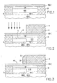
- FIG. 1 A preferred process for fabricating the transistor configuration of Fig. 8 will now be described with reference to Figs. 1-7.
- the process begins with a P+ substrate 32 with a P- epitaxial layer 32 grown thereover.
- the steps required in order to obtain a P- epitaxial layer growth are well known in the art and reference is made to VLSI Technology by S.M. SZE, Chap. 2, Wiley & Sons.
- this isolation scheme may comprise a fully recessed oxide type of isolation, a more conventional semi-ROX isolation, some type of trench isolation, or a variety of other different isolation configurations utilizing available insulation materials.
- a fully recessed oxide isolation scheme is shown in Fig. 1.
- the recessed oxide layers are represented in Fig. 1 by the areas 36 and 38.
- the volume 40 which will eventually include the collector region 12 (not shown in Fig. 1) is formed on on the P- epi layer 34.
- This region 40 is formed by doping the region with an appropriate dopant to a desired concentration.
- the region 40 is doped with an N-type dopant such as phosphorus to a concentration of 1E17 per cubic centimeter.
- a variety of methods of doping may be utilized to obtain the region 40 including ion implantation.
- the depth of the implant is based on design considerations and may typically be on the order of 6000 Angstroms.
- a region 14 which will become the base layer must be formed thereover.
- a P type ion implant may be utilized to form a P doped region 14 to a depth of about 2000 Angstroms.
- the next region to be formed is to be used to implement the emitter layer 16.
- This layer 16 may be formed by using either an additional N+ doping step, or by depositing an additional N+ doped layer thereover.
- an N+ doped layer of polysilicon is deposited over the wafer to form the emitter layer 16.
- the thickness for this emitter layer 16 may be on the order of 1500 Angstroms.
- a narrow-width emitter is advantageous because it significantly reduces the area component of capacitance between the emitter and the base without an overly severe increase of the resistance of the configuration.
- most of the current flows through the edge regions of the emitter and the base, with the center region thereof contributing only a nominal amount of current to the device operation.
- the reduction of the emitter width does not affect the current flow while significantly reducing the capacitance of the device.
- the narrow emitter configuration uses the fact that a typical emitter-base diode junction is heavily turned on only in the region close to the base contacts, to provide a design which reduces the device capacitance.
- the sidewall image transfer technique may be implemented by first forming a step 42 of insulating material, such as an organic material, over a first portion 44 of the top surface of emitter layer 16, but not over a second portion 46 thereof.
- the step 42 may be formed by means of standard lithography techniques.
- the step thickness will typically be on the order of 2.0 microns.
- a subcollector region 28 may be formed in the device in the region below the second portion 46 of the top surface of the emitter layer 16.
- This subcollector formation may be accomplished, by way of example, by means of a relatively high-energy ion implantation to form the subcollector layer 28.
- a relatively high-energy ion implantation to form the subcollector layer 28.
- an ion implantation with phosphorus ions with energies of on the order of 700KeV with may be utilized.
- the subcollector region could have been formed by means of some form of deposition or doping step at an earlier point in the process.
- the present invention is not limited to the particular method or the timing, at which the subcollector layer is formed in the device.
- the step 42 is on the order of 2.0 microns in thickness, none of the phosphorus ions penetrate into the silicon area beneath the step 42.
- the ion implantation energy is also low enough to maintain an N doped layer 12 between the subcollector layer 28 and the base layer 14.
- the appropriate dosage may be calculated for different transistor configurations by means of standard LSS statistical analysis using Gaussian distribution information.
- the next step in forming the present bipolar transistor configuration is to form a sidewall spacer 48 of insulating material against the sidewall of the step 42 to thereby cover a third portion 50 of the top surface of the emitter layer 16, which third portion 50 is less in area than the second portion 46.
- this sidewall spacer formation may be accomplished coating the configuration of Fig. 2 with a layer of some form of insulating material such as SiO2 or Si3N4 to a thickness which may be on the order of 5000 Angstroms. This coating may be applied by means, for example, of a plasma deposition.
- the maximum temperature of this deposition for the insulating layer should be limited. In this regard, it is noted that excellent conformality of SiO2 or Si3N4 is achieved at temperatures of less than 300_C. It has been found that such temperatures do not adversely affect the organic material of the step 42.
- a directional dry etch (RIE) of the plasma deposited insulating layer is then used to remove the horizontal portions of this insulating layer while leaving the spacer 48 disposed against the edge of the step material 42.
- the horizontal width of the spacer 48 depends primarily on the thickness of the deposition of the insulating layer, on the system's conformality, and on the directionality of the etch medium utilized. In this configuration, the preferred etch should be selective to polysilicon. By way of example, a CF4 + H2 mixture may be utilized as the etching gas.
- the resulting spacer 48 will have a width of on the order of 5000 Angstroms.
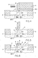
- the next step in forming the transistor configuration of the present invention is illustrated in Fig. 4 and comprises removing the emitter layer 16 and at least a nominal portion of the base layer 14 in a first volume directly adjacent to the sidewall spacer 48.
- This removal step may be accomplished conveniently by a selective etch of the polysilicon layer 16.
- a typical selective etching medium that may be utilized is Freon 11 + N2 + O2 or Freon 11 + AIR. Utilizing this etching medium, the spacer will only be minimally etched and will remain in tact. Note that the standard overetch of the polysilicon layer 16 into the P base layer 14 will not adversely affect the device configuration.
- This increase in concentration may be accomplished conveniently by an ion implantation (represented by the arrows 52 in Fig. 4) into that region adjacent to the spacer 48.
- an ion implantation of phosphorus ions at an energy of on the order of 200KeV may be utilized in order to increase the doping concentration in the area 30 adjacent to the sidewall spacer to a concentration of N++.
- this raised concentration in the region 30 will be in the range of 1E20 per cubic centimeter.
- step 42 it is desirable to remove the step 42.
- a variety of different procedures may be utilized to remove the step 42 depending on the step material.
- the step may be removed simply by ashing in an oxygen plasma. The resulting configuration is shown in Fig. 5.
- the emitter layer removal may be accomplished simply by an etch step formulated to remove the particular material used for the emitter.
- the polysilicon layer 16 below the step may be reactive ion etched using a gas mixture of SF6 + Cl2 or Fr11 O2 + N2.
- the silicon surface on the other side of the sidewall spacer 48 continues to be exposed. Accordingly, the reactive ion etching gas operates to etch this silicon down to the implanted N++ region 30.
- the next step in the process is to remove the sidewall spacer 48. It is preferred that a selective etch formulated to only select the sidewall spacer material be utilized.
- an HF etch may be utilized for SiO2, or a hot H3PO4 etch may be utilized for Si3N4.
- an HF etch mixture was utilized to remove an SiO2 sidewall spacer 48. It should be noted that plasma-generated SiO2 etches more quickly than thermally grown SiO2 or LPCVD SiO2 deposited and densified at higher temperatures. Accordingly, the removal of the plasma-deposited spacer 48 does not thin the isolation regions 36 and 38 to any hazardous extent. Note that if Si3N4 had been used, the suggested H3NO4 etch does not harm SiO2 at all, and the temperature for this etch can be lowered to avoid etching the N+ polysilicon if there is any sensitivity in this area.
- the thin emitter length there are a variety of different methods which may be utilized to define the emitter length.
- a photoresist mask may be applied on the emitter and a selective reactive ion etch of the polysilicon utilized to remove sections of the polysilicon 16 where it is desired to cut the polysilicon line.
- This step is required because of the inherent nature of sidewall image transfer.
- the sidewall image transfer process typically results in the formation of a sidewall in a closed shape around a particular step. Accordingly, all of the submicron width sidewall lines are formed in closed shapes.
- a photoresist mask must thus be used in order to remove those portions of the closed shape which are not desirable for the device configuration.
- the resulting emitter line length may be on the order of 1.0 micron or less.
- a first insulator sidewall 18 is formed in the first volume adja cent to and in contact with one side of the emitter layer 16, the base layer 14, and at least a nominal portion of the collector layer 12 and touching the collector contact surface 64.
- a second insulator sidewall 20 is formed in the second volume adjacent to and in contact with another side of the emitter layer 16, and at least a nominal portion of the base layer 14, and touching the base contact surface 62.
- these insulator sidewalls 18 and 20 may be formed simply by coating the configuration with an approximately 2000 Angstrom thick deposition oxide (plasma SiO2 or TEOS).
- plasma SiO2 or TEOS approximately 2000 Angstrom thick deposition oxide
- a directional etch using, for example, a reactive ion etching gas mixture of CF4 + H2 may be utilized to form the spacers on the sides of the emitter 16 used to provide the isolation for the vertical edge of the device. Note that the asymmetry in the contact surface height on either side of the emitter does not adversely affect the spacer formation.
- a shallow P+ type implant is then used to raise the P type doping concentration in the base contact extension layer 72.
- the energy of the ion implant is chosen so that it does not penetrate the N+ polysilicon emitter layer 16 and the ion dosage is designed so that it doesn't compensate either the N+ emitter polySi or the N++ doping of the region 30 in the collector contact extension layer 26, but will effectively raise the doping level of the extrinsic base for contact purposes.
- an implant energy of 40KeV of BF2 ions at a dosage of 8E14 per square centimeter may be utilized.
- the result of this ion implantation step is a P+ layer 74, shown in Fig. 7.
- a rapid thermal anneal may then be performed to activate the P+ dopant (cause the dopant atoms to introduce holes) without any considerable junction movement to thereby form the base contact extension layer 22.
- a silicide is generally formed over the collector, emitter, and base contact surfaces.
- Ti or some other silicide-forming metal may be deposited and reacted with the exposed silicon on the contact surfaces to provide self-aligned silicide over the collector, emitter, and base contact surfaces. The unreacted metal is then removed selectively, leaving the silicide.
- Well-known processes may be used to form the contact interconnects to these self-aligned silicide contact layers.
- the resulting device has a contact to the collector layer 12 by means of the collector contact extension layer 26 (28 and 30).
- a contact to the base layer 14 is obtained by means of the base contact extension layer 22, and contact to the emitter 16 is obtained by direct contact to the polysilicon line forming the emitter when the line is brought out onto an isolation region.
- a top view of this contact structure is shown in Fig. 9.
- the emitter polysilicon line 16 is shown in the center of the Figure.
- the N++ surface 64 for the collector contact extension layer 26 is shown to the left of the submicron emitter 16.
- the top surface 62 for the P+ region of the base contact extension layer 22 is shown to the right of the submicron emitter line 16.
- the contact hole for the collector is designated 80
- the contact hole for the emitter is designated 82
- the contact hole for the base is designated 84.
- the emitter layer 16 there can be leakage from the emitter layer 16 to the collector layer 12 by means of a parasitic vertical FET device formed on the edge of the base layer 14.
- This parasitic FET device may be formed if the sidewall adjacent to the base becomes inverted.
- this inversion may be caused by the low doping level of the base layer 14 and the increased surface state level present on the edge of the base layer 14. Both of these factors tend to reduce the threshold voltage for charge leakage thereacross.
- the base sidewall surface can invert causing a low current path from the emitter 16 to the collector 12.
- the sidewall spacers 18 and 20 shown in Fig. 8 could be doped spacers in order to inhibit inversion adjacent to the vertical base edge.
- the sidewall spacers 18 and 20 may be formed of borosilicate glass.
- a low temperature of on the order of 800_C may be used to drive in the boron from the spacer to the silicon vertical edge of the base 14. This drive-in of the boron to the base vertical edge effectively raises the base doping at the edge which is in contact with the oxide spacer, thereby inhibiting inversion thereof.
- the amount of boron used in the borosilicate glass would not be sufficient to cause compensation at the vertical sidewall edge for either the collector 12 or the emitter 16.
- a preferred borosilicate glass concentration is 4%.
- a P+ type implant 90 is formed on the volume directly below the surface 60.
- This P+ type implant may be implemented by boron ions at a concentration of 1E14 per cubic centimeter.
- This P+ implant is then followed by the formation of an additional spacer 92 in order to widen the already existing spacer 48.
- the formation of this additional spacer 92 may be accomplished by depositing a desired thickness of a spacer material, for example, 1000 Angstroms, and then directionally etching that deposited layer to leave only the vertical spacer 92.
- the P+ doped region 90 will be eliminated, except for the P+ doped region 94 disposed directly below the additional spacer 92.
- This additional P+ doped region 94 disposed adjacent to the vertical edge of the base layer 14 will inhibit the inversion of the vertical wall of this base layer.
- the additional spacer 92 is removed with the previously existing spacer 48.
- the present inventive structure and process yields a device configuration which significantly enhances the number of transistors which may be formed on a given substrate.
- the present configuration avoids the use of the standard symmetric base contact on either side of the emitter, and also avoids the use of the standard reach-thru contact to the subcollector.
- the base contact extension layer is at a higher level than the collector contact extension layer.
- the structure resulting from the present invention has high performance.
- the described process advantageously uses sidewall image transfer to form very narrow emitters of on the order of 0.4 microns or less. These narrow emitters lead to the high performance characteristic. Additionally, these narrow emitters reduce the base resistance and minimize parasitic capacitance due to the reduced area of the base so that the performance is increased to on the order of 40 gigahertz or greater.
- the processing for the device configuration is relatively simple compared to other advanced bipolar structures. For example, there is no reach-thru structure. Additionally, no high temperature drive-in steps are required for the subcollector in the present configuration. Finally, in the embodiment of the invention wherein the subcollector is implanted, no epitaxial growth is required after the subcollector is formed. This fabrication methodology is compatible with FET type processes.
Abstract
Description
- The present invention relates generally to bipolar transistors, and more particularly to an advanced vertical bipolar transistor structure and process.
- A basic goal in bipolar circuit design is to reduce the circuit power consumption while, at the same time, increasing the speed of operation. One way to reduce power consumption is to utilize BIFET (bipolar and FET) circuits. To this end, it is highly desirable that any bipolar process be compatible with FET processing so that BIFET (bipolar and FET) chip configurations can be implemented. However, these design goals must be implemented with a transistor fabrication process that is economical.
- The invention as claimed is intended to provide a bipolar transistor which offers increased speed of operation. An advantage offered by the present invention is that the need for a subcollector reach-thru contact is eliminated. A further advantage of the present invention is the overall width of the transistor is reduced by eliminating the need for the standard base contact that is normally disposed between the emitter and collector contacts. An additional advantage of the present invention is that a very narrow emitter is utilized, effectively resulting in a reduction of the problems associated with intrinsic base resistance and a minimization of emitter-base capacitance. Moreover, the process that may be used to implement the transistor design of the present invention is relatively simple and is compatible with FET processing.
- Briefly, the present invention is a bipolar transistor, comprising:
a collector layer;
a base layer disposed over the collector layer;
an emitter layer disposed over the base layer;
a first sidewall insulating layer disposed adjacent to and in contact with one side of the emitter layer, the base layer, and at least a portion of the collector layer;
a second sidewall insulating layer disposed adjacent to and in contact with another side of the emitter layer and at least a portion of the base layer;
a base contact extension layer formed from heavily doped semiconductor material of the same conductivity type as the base layer, said base contact extension layer being in contact with and extending laterally from another side of the base layer;
a base contact interconnect disposed on a surface of the base contact extension layer;
a collector contact extension layer formed from doped semiconductor material with the same conductivity type as the collector layer, with the collector contact extension layer being in contact with the collector layer and extending laterally from or below the one side thereof; and
a collector contact interconnect disposed on a surface of the collector contact extension layer and separated from the emitter layer by only one or more insulating layers. - In a preferred embodiment, the base contact extension layer is in lateral contact with the base layer, and the collector contact extension layer is in contact with the bottom surface of the collector layer.
- Additionally, it is preferred that the top surface of the collector contact extension layer be below the top surface of the base contact extension layer. Finally, it is preferred that the bottom surface of the base contact extension layer be above the top surface of the collector contact extension layer.
- In a further embodiment of the present invention, it is preferred that the emitter layer have a width of less than one micron.
- The present invention further includes a preferred method for fabricating the present bipolar transistor. This method comprises the steps of:
obtaining a structure comprising a collector layer, a base layer disposed over the collector layer, an emitter layer disposed over the base layer, a step in a layer of insulating material disposed over a first portion of the top surface of the emitter layer, but not over a second portion thereof, and a subcollector disposed at least below the collector layer in the region below the second portion of the top surface of the emitter layer;
forming a sidewall spacer of insulating material against the approximately vertical edge of the step in the insulating layer to thereby cover a third portion of the top surface of the emitter layer, which third portion is less than the second portion;
removing the emitter layer and at least a portion of the base layer in a first volume adjacent to the sidewall spacer;
removing the insulating layer step;
removing the emitter layer and a portion of the base layer in a second volume below the removed step to expose the base layer and provide a base contact surface, and also removing additional material in the first volume in order to expose a collector contact surface which is lower relative to the base contact surface;
removing the sidewall spacer;
forming simultaneously a first insulator sidewall in the first volume adjacent to and in contact with one side of the emitter layer, base layer and at least a portion of said collector layer and touching the collector contact surface, and a second insulator sidewall in the second volume adjacent to and in contact with another side of the emitter layer and at least a portion of the base layer, and touching the base contact surface; and
forming a collector contact interconnect on the top surface of the exposed collector contact surface and a base contact interconnect to the top surface of the exposed base contact surface. - Fig. 1 is a schematic diagram of a semiconductor substrate during an initial part of the inventive process.
- Fig. 2 is a schematic diagram of the semiconductor substrate after a step has been disposed thereover.
- Fig. 3 is a schematic diagram of the substrate after a spacer has been disposed adjacent to the step.
- Fig. 4 is a schematic diagram of the semiconductor substrate after etching and ion implantation steps have been performed.
- Fig. 5 is a schematic diagram of the semiconductor substrate after removal of the step and after a second etching procedure has been performed.
- Fig. 6 is a schematic diagram of the semiconductor substrate after the formation of sidewall insulator layers.
- Fig. 7 is a schematic diagram of the semiconductor substrate after the formation of a P+ region adjacent to the base layer.
- Fig. 8 is a schematic diagram of the transistor resulting from the present inventive process.
- Fig. 9 is a schematic top-view of the transistor formed in accordance with the present process.
- Fig. 10A is a schematic diagram of the device configuration after the performance of one step in a process to prevent low E-C punch-through.
- Fig. 10B is a schematic diagram of the device configuration after the performance of a second step in a process to prevent low E-C punch-through in the transistor.
- Fig. 10C is a schematic diagram of the device configuration after the performance of a third step in a process to prevent low E-C punch-through in the transistor.
- The present invention is illustrated, for convenience, in the context of an NPN transistor configuration. It is understood by one skilled in the art that the present invention is not limited to this particular configuration, but may take a variety of other configurations including PNP transistor configurations. Additionally, the present invention is not restricted to the particular dimensions and proportions shown in the drawings. The present invention may be implemented in a number of different semiconductor materials including Si and GaAs.
- Referring now to Fig. 8, there is shown the
bipolar transistor configuration 10 of the present invention. This transistor comprises acollector layer 12, abase layer 14 disposed over thecollector layer 12, and anemitter layer 16 disposed over thebase layer 14. The transistor configuration further includes asidewall insulator layer 18 disposed adjacent to and in contact with the one side of theemitter layer 16, thebase layer 14, and at least a nominal portion of thecollector layer 12. The configuration further includes a secondsidewall insulating layer 20 disposed adjacent to and in contact with another side of theemitter layer 16 and at least a nominal portion of thebase layer 14. Note that in the embodiment shown in Fig. 8, this other side of the emitter layer is conveniently the opposite side from the one side of the emitter layer where the firstsidewall insulating layer 18 is disposed. The transistor configuration further includes a basecontact extension layer 22 formed from heavily doped semiconductor material of the same conductivity type as thebase layer 14, in contact with and extending laterally from another side of thebase layer 14. Abase contact interconnect 24 is disposed on thetop surface 62 of the basecontact extension layer 22, separated from the emitter layer by only one or more insulating layers. The configuration further includes a collectorcontact extension layer 26 formed from heavily doped semiconductor material with the same conductivity type as thecollector layer 12, with the collectorcontact extension layer 26 being in contact with the collector layer and extending laterally from or below the one side thereof. It can be seen that this collectorcontact extension layer 26 in the embodiment shown in Fig. 8 actually contacts the bottom surface of thecollector layer 12 and extends laterally to the left of the transistor configuration. Finally, acollector contact interconnect 29 is disposed on the collectorcontact extension layer 26 on thecontact surface 64, separated from theemitter layer 16 by only one or more insulating layers. - It should be noted that in a preferred embodiment, the collector
contact extension layer 26 comprises afirst portion 28, which is a subcollector layer, disposed directly below and in contact with thecollector layer 12 and having a first dopant concentration, and asecond portion 30 with a dopant concentration which is greater than the first dopant concentration and which is disposed directly below thesurface 64 of the collector contact extension layer in the volume which extends to one side of thecollector layer 12. - By way of illustration, and not by way of limitation, the embodiment shown in Fig. 8 utilizes a
collector layer 12 which is doped to an N- concentration, abase layer 14 which is doped to a P concentration,emitter layer 16 which is doped to an N+ concentration, a basecontact extension layer 22 which is doped to a P+ concentration, and a collectorcontact extension layer 26 with afirst portion 28 thereof (the subcollector layer) doped to an N+ concentration and asecond portion 30 thereof which is doped to an N++ concentration. - By way of example, the present bipolar transistor configuration shown in Fig. 8 may be formed on a
P+ substrate 32 with a P-epitaxial layer 34 grown thereon. An isolation scheme using some form ofinsulator portions bipolar transistor 10 from other chip components. In the embodiment of Fig. 8, thebase insulator portions - The above-described bipolar transistor configuration significantly reduces the width of the overall transistor by eliminating the inside base contact normally situated between the emitter and collector contacts. This reduced transistor width significantly increases the number of active devices which can be integrated onto a chip.
- A preferred process for fabricating the transistor configuration of Fig. 8 will now be described with reference to Figs. 1-7. Referring first to Fig. 1, the process begins with a
P+ substrate 32 with a P-epitaxial layer 32 grown thereover. The steps required in order to obtain a P- epitaxial layer growth are well known in the art and reference is made to VLSI Technology by S.M. SZE, Chap. 2, Wiley & Sons. - Some form of isolation scheme may be conveniently executed at this point in the process. By way of example, this isolation scheme may comprise a fully recessed oxide type of isolation, a more conventional semi-ROX isolation, some type of trench isolation, or a variety of other different isolation configurations utilizing available insulation materials. For simplicity of explanation of the present invention, a fully recessed oxide isolation scheme is shown in Fig. 1. The recessed oxide layers are represented in Fig. 1 by the
areas - After the formation of the isolation scheme volumes, the
volume 40 which will eventually include the collector region 12 (not shown in Fig. 1) is formed on on the P-epi layer 34. Thisregion 40 is formed by doping the region with an appropriate dopant to a desired concentration. For the present example embodiment of an NPN transistor, theregion 40 is doped with an N-type dopant such as phosphorus to a concentration of 1E17 per cubic centimeter. A variety of methods of doping may be utilized to obtain theregion 40 including ion implantation. The depth of the implant is based on design considerations and may typically be on the order of 6000 Angstroms. - After the N-
region 40 is formed, aregion 14 which will become the base layer must be formed thereover. By way of example, a P type ion implant may be utilized to form a P dopedregion 14 to a depth of about 2000 Angstroms. - The next region to be formed is to be used to implement the
emitter layer 16. Thislayer 16 may be formed by using either an additional N+ doping step, or by depositing an additional N+ doped layer thereover. In the present embodiment, an N+ doped layer of polysilicon is deposited over the wafer to form theemitter layer 16. The thickness for thisemitter layer 16 may be on the order of 1500 Angstroms. - In a preferred embodiment, it is desirable to have a very narrow-width emitter. A narrow-width emitter is advantageous because it significantly reduces the area component of capacitance between the emitter and the base without an overly severe increase of the resistance of the configuration. In this regard, most of the current flows through the edge regions of the emitter and the base, with the center region thereof contributing only a nominal amount of current to the device operation. Thus, the reduction of the emitter width does not affect the current flow while significantly reducing the capacitance of the device. In essence, the narrow emitter configuration uses the fact that a typical emitter-base diode junction is heavily turned on only in the region close to the base contacts, to provide a design which reduces the device capacitance.
- In order to obtain this narrow-
width emitter layer 16, a variety of different techniques may be utilized. In a preferred embodiment, a technique called sidewall image transfer may be used. This technique is described in detail in U.S. Patent No. 4,648,937. - Referring now to Fig. 2, the sidewall image transfer technique may be implemented by first forming a
step 42 of insulating material, such as an organic material, over afirst portion 44 of the top surface ofemitter layer 16, but not over asecond portion 46 thereof. Thestep 42 may be formed by means of standard lithography techniques. The step thickness will typically be on the order of 2.0 microns. - At this point in the process, a
subcollector region 28 may be formed in the device in the region below thesecond portion 46 of the top surface of theemitter layer 16. This subcollector formation may be accomplished, by way of example, by means of a relatively high-energy ion implantation to form thesubcollector layer 28. By way of example, an ion implantation with phosphorus ions with energies of on the order of 700KeV with may be utilized. It should be noted that the subcollector region could have been formed by means of some form of deposition or doping step at an earlier point in the process. The present invention is not limited to the particular method or the timing, at which the subcollector layer is formed in the device. Note that because thestep 42 is on the order of 2.0 microns in thickness, none of the phosphorus ions penetrate into the silicon area beneath thestep 42. The ion implantation energy is also low enough to maintain an N dopedlayer 12 between thesubcollector layer 28 and thebase layer 14. Note that the appropriate dosage may be calculated for different transistor configurations by means of standard LSS statistical analysis using Gaussian distribution information. - Referring now to Fig. 3, the next step in forming the present bipolar transistor configuration is to form a
sidewall spacer 48 of insulating material against the sidewall of thestep 42 to thereby cover athird portion 50 of the top surface of theemitter layer 16, whichthird portion 50 is less in area than thesecond portion 46. By way of example, this sidewall spacer formation may be accomplished coating the configuration of Fig. 2 with a layer of some form of insulating material such as SiO₂ or Si₃N₄ to a thickness which may be on the order of 5000 Angstroms. This coating may be applied by means, for example, of a plasma deposition. If an organic material is utilized to form thestep 42, then it should be noted that the maximum temperature of this deposition for the insulating layer should be limited. In this regard, it is noted that excellent conformality of SiO₂ or Si₃N₄ is achieved at temperatures of less than 300_C. It has been found that such temperatures do not adversely affect the organic material of thestep 42. - A directional dry etch (RIE) of the plasma deposited insulating layer is then used to remove the horizontal portions of this insulating layer while leaving the
spacer 48 disposed against the edge of thestep material 42. The horizontal width of thespacer 48 depends primarily on the thickness of the deposition of the insulating layer, on the system's conformality, and on the directionality of the etch medium utilized. In this configuration, the preferred etch should be selective to polysilicon. By way of example, a CF₄ + H₂ mixture may be utilized as the etching gas. The resultingspacer 48 will have a width of on the order of 5000 Angstroms. - The next step in forming the transistor configuration of the present invention is illustrated in Fig. 4 and comprises removing the
emitter layer 16 and at least a nominal portion of thebase layer 14 in a first volume directly adjacent to thesidewall spacer 48. This removal step may be accomplished conveniently by a selective etch of thepolysilicon layer 16. A typical selective etching medium that may be utilized is Freon 11 + N₂ + O₂ or Freon 11 + AIR. Utilizing this etching medium, the spacer will only be minimally etched and will remain in tact. Note that the standard overetch of thepolysilicon layer 16 into theP base layer 14 will not adversely affect the device configuration. - It is desirable to raise the concentration of the
subcollector region 28 where it extends out from under thespacer region 48. The purpose of this increase in concen tration is to lower the contact resistance to this area. This increase in concentration may be accomplished conveniently by an ion implantation (represented by thearrows 52 in Fig. 4) into that region adjacent to thespacer 48. By way of example, an ion implantation of phosphorus ions at an energy of on the order of 200KeV may be utilized in order to increase the doping concentration in thearea 30 adjacent to the sidewall spacer to a concentration of N++. Typically, this raised concentration in theregion 30 will be in the range of 1E20 per cubic centimeter. - At this point in the process it is desirable to remove the
step 42. A variety of different procedures may be utilized to remove thestep 42 depending on the step material. By way of example, for an organic step material, the step may be removed simply by ashing in an oxygen plasma. The resulting configuration is shown in Fig. 5. - After the removal of the
step 42, it is now desirable to remove the emitter layer and a portion of the base layer in a second volume below the removedstep 42 in order to expose thebase layer 14 and provide abase contact surface 62. This emitter layer removal may be accomplished simply by an etch step formulated to remove the particular material used for the emitter. In the present example, thepolysilicon layer 16 below the step may be reactive ion etched using a gas mixture of SF₆ + Cl₂ or Fr₁₁ O₂ + N₂. During this etching step, in a preferred process embodiment, the silicon surface on the other side of thesidewall spacer 48 continues to be exposed. Accordingly, the reactive ion etching gas operates to etch this silicon down to the implantedN++ region 30. The resulting configuration at this point in the process is shown in Fig. 5. It can be seen that thetop surface 64 of theN++ region 30 is now exposed. Additionally, it can be seen that theP region 14 on the other side of thespacer 48 is exposed at thesurface 62. - Referring now to Fig. 6, the next step in the process is to remove the
sidewall spacer 48. It is preferred that a selective etch formulated to only select the sidewall spacer material be utilized. In the present example embodiment, an HF etch may be utilized for SiO₂, or a hot H₃PO₄ etch may be utilized for Si₃N₄. In the present example, an HF etch mixture was utilized to remove anSiO₂ sidewall spacer 48. It should be noted that plasma-generated SiO₂ etches more quickly than thermally grown SiO₂ or LPCVD SiO₂ deposited and densified at higher temperatures. Accordingly, the removal of the plasma-depositedspacer 48 does not thin theisolation regions - At this point in the process, it is convenient to define the thin emitter length. There are a variety of different methods which may be utilized to define the emitter length. By way of example, a photoresist mask may be applied on the emitter and a selective reactive ion etch of the polysilicon utilized to remove sections of the
polysilicon 16 where it is desired to cut the polysilicon line. This step is required because of the inherent nature of sidewall image transfer. In this regard, the sidewall image transfer process typically results in the formation of a sidewall in a closed shape around a particular step. Accordingly, all of the submicron width sidewall lines are formed in closed shapes. A photoresist mask must thus be used in order to remove those portions of the closed shape which are not desirable for the device configuration. The resulting emitter line length may be on the order of 1.0 micron or less. - At this point in the process it is desirable to form, preferably simultaneously, a set of insulator sidewalls to insulate the sides of the emitter, base, and collector which are exposed. Referring now to Fig. 6, a
first insulator sidewall 18 is formed in the first volume adja cent to and in contact with one side of theemitter layer 16, thebase layer 14, and at least a nominal portion of thecollector layer 12 and touching thecollector contact surface 64. Simultaneously, asecond insulator sidewall 20 is formed in the second volume adjacent to and in contact with another side of theemitter layer 16, and at least a nominal portion of thebase layer 14, and touching thebase contact surface 62. In a preferred embodiment, these insulator sidewalls 18 and 20 may be formed simply by coating the configuration with an approximately 2000 Angstrom thick deposition oxide (plasma SiO₂ or TEOS). A directional etch using, for example, a reactive ion etching gas mixture of CF₄ + H₂ may be utilized to form the spacers on the sides of theemitter 16 used to provide the isolation for the vertical edge of the device. Note that the asymmetry in the contact surface height on either side of the emitter does not adversely affect the spacer formation. - A shallow P+ type implant is then used to raise the P type doping concentration in the base contact extension layer 72. The energy of the ion implant is chosen so that it does not penetrate the N+
polysilicon emitter layer 16 and the ion dosage is designed so that it doesn't compensate either the N+ emitter polySi or the N++ doping of theregion 30 in the collectorcontact extension layer 26, but will effectively raise the doping level of the extrinsic base for contact purposes. By way of example, as an implant energy of 40KeV of BF2 ions at a dosage of 8E14 per square centimeter may be utilized. The result of this ion implantation step is aP+ layer 74, shown in Fig. 7. A rapid thermal anneal may then be performed to activate the P+ dopant (cause the dopant atoms to introduce holes) without any considerable junction movement to thereby form the basecontact extension layer 22. - In order to form appropriate device contact interconnects, a silicide is generally formed over the collector, emitter, and base contact surfaces. By way of example, Ti or some other silicide-forming metal may be deposited and reacted with the exposed silicon on the contact surfaces to provide self-aligned silicide over the collector, emitter, and base contact surfaces. The unreacted metal is then removed selectively, leaving the silicide. Well-known processes may be used to form the contact interconnects to these self-aligned silicide contact layers.
- The resulting device has a contact to the
collector layer 12 by means of the collector contact extension layer 26 (28 and 30). A contact to thebase layer 14 is obtained by means of the basecontact extension layer 22, and contact to theemitter 16 is obtained by direct contact to the polysilicon line forming the emitter when the line is brought out onto an isolation region. A top view of this contact structure is shown in Fig. 9. Theemitter polysilicon line 16 is shown in the center of the Figure. TheN++ surface 64 for the collectorcontact extension layer 26 is shown to the left of thesubmicron emitter 16. Likewise, thetop surface 62 for the P+ region of the basecontact extension layer 22 is shown to the right of thesubmicron emitter line 16. The contact hole for the collector is designated 80, the contact hole for the emitter is designated 82, and the contact hole for the base is designated 84. - It is noted that in some instances it is possible that there can be leakage from the
emitter layer 16 to thecollector layer 12 by means of a parasitic vertical FET device formed on the edge of thebase layer 14. This parasitic FET device may be formed if the sidewall adjacent to the base becomes inverted. In particular, this inversion may be caused by the low doping level of thebase layer 14 and the increased surface state level present on the edge of thebase layer 14. Both of these factors tend to reduce the threshold voltage for charge leakage thereacross. Thus, the base sidewall surface can invert causing a low current path from theemitter 16 to thecollector 12. Alternatively, there may be E-C punch- through. In order to avoid this inversion and leakage or punch-through problem, thesidewall spacers sidewall spacers spacers base 14. This drive-in of the boron to the base vertical edge effectively raises the base doping at the edge which is in contact with the oxide spacer, thereby inhibiting inversion thereof. However, the amount of boron used in the borosilicate glass would not be sufficient to cause compensation at the vertical sidewall edge for either thecollector 12 or theemitter 16. A preferred borosilicate glass concentration is 4%. - Another method which could be utilized before the N++ implant step shown in Fig. 4 has been performed, is illustrated in Fig. 10A. In Fig. 10A a
P+ type implant 90 is formed on the volume directly below thesurface 60. This P+ type implant may be implemented by boron ions at a concentration of 1E14 per cubic centimeter. This P+ implant is then followed by the formation of anadditional spacer 92 in order to widen the already existingspacer 48. The formation of thisadditional spacer 92 may be accomplished by depositing a desired thickness of a spacer material, for example, 1000 Angstroms, and then directionally etching that deposited layer to leave only thevertical spacer 92. When the subsequent N++ implant step is performed in Fig. 4 in order to form the highly dopedregion 30, and thepolySi emitter layer 16 is etched above thebase region 62 in Fig. 5, the P+ dopedregion 90 will be eliminated, except for the P+ dopedregion 94 disposed directly below theadditional spacer 92. This additional P+ dopedregion 94 disposed adjacent to the vertical edge of thebase layer 14 will inhibit the inversion of the vertical wall of this base layer. Theadditional spacer 92 is removed with the previously existingspacer 48. - The present inventive structure and process yields a device configuration which significantly enhances the number of transistors which may be formed on a given substrate. In particular, the present configuration avoids the use of the standard symmetric base contact on either side of the emitter, and also avoids the use of the standard reach-thru contact to the subcollector. In one embodiment of this configuration, the base contact extension layer is at a higher level than the collector contact extension layer.
- The structure resulting from the present invention has high performance. The described process advantageously uses sidewall image transfer to form very narrow emitters of on the order of 0.4 microns or less. These narrow emitters lead to the high performance characteristic. Additionally, these narrow emitters reduce the base resistance and minimize parasitic capacitance due to the reduced area of the base so that the performance is increased to on the order of 40 gigahertz or greater.
- An additional point with respect to the present invention is that the processing for the device configuration is relatively simple compared to other advanced bipolar structures. For example, there is no reach-thru structure. Additionally, no high temperature drive-in steps are required for the subcollector in the present configuration. Finally, in the embodiment of the invention wherein the subcollector is implanted, no epitaxial growth is required after the subcollector is formed. This fabrication methodology is compatible with FET type processes.
- While the present invention has been particularly shown and described with reference to preferred embodiments therefor, it will be understood by those skilled in the art that the foregoing and other changes in form and detail will be made therein without departing from the scope and spirit of the present invention.
Claims (21)
a subcollector layer of semiconductor material;
a collector layer of semiconductor material doped with a dopant having first conductivity type, said collector layer being disposed over said subcollector layer;
a base layer of semiconductor material doped with a dopant having a second conductivity type, said base layer being disposed over said collector layer;
an emitter layer of semiconductor material disposed over said base layer;
a first layer of semiconductor material that is doped with a dopant having said second conductivity type and with a doping concentration greater than said base doping concentration, said first layer being disposed in contact with and laterally adjacent to one side of said base layer, but with a top surface thereof that is below the bottom surface of said emitter layer, but above the top surface of said collector layer;
a first sidewall insulator layer disposed laterally adjacent to and in contact with said emitter and on the same side thereof as said first layer of semiconductor material;
a base contact interconnect disposed on said top surface of said first layer and separated from said emitter layer by only one or more insulating layers;
a second layer of semiconductor material that is heavily doped with a dopant having said first conductivity type (e.g. at least N+ or P+ doping), said second layer being disposed in contact with and laterally adjacent to said subcollector layer and on another side of said emitter than said first layer of semiconductor material, but with a top surface there of that is below the top surface of said collector layer; and
a second sidewall insulator layer disposed laterally adjacent to and in contact with said emitter layer, said base layer, and at least a nominal portion of said collector layer, and on said another side of said emitter layer than said first layer; and
a collector contact interconnect disposed on said top surface of said second layer and separated from said emitter layer by only one or more insulating layers.
a collector layer of doped semiconductor material;
a base layer of doped semiconductor material disposed over said collector layer;
an emitter layer of doped semiconductor material disposed over said base layer;
a first sidewall insulating layer disposed adjacent to and in contact with one side of said emitter layer, said base layer, and at least a nominal portion of said collector layer;
a second sidewall insulating layer disposed adjacent to and in contact with another side of said emitter layer and at least a nominal portion of said base layer;
a base contact extension layer formed from doped semiconductor material of the same conductivity type as said base layer in contact with and extending laterally from said another side of said base layer;
a base contact interconnect disposed on a surface of said base contact extension layer and separated from said emitter layer by only one or more insulator layers;
a collector contact extension layer formed from heavily doped semiconductor material with the same conductivity type as said collector layer, said collector contact extension layer being in contact with said collector layer with a volume thereof extending laterally to said one side thereof; and
a collector contact interconnect disposed on a surface of said collector contact extension layer and disposed adjacent to and separated from said emitter layer by only one or more insulator layers.
obtaining a structure comprising a collector layer of doped semiconductor material, a base layer of doped semiconductor material disposed over said collector layer, an emitter layer of doped semiconductor material disposed over said base layer, a step of insulating material disposed over a first portion of the top surface of said emitter layer, but not over a second portion thereof, and a subcollector disposed below said collector layer in the region below said second portion of said top surface of said emitter layer;
forming a sidewall spacer of insulating material against the sidewall of said step to thereby cover a third portion of the top surface of said emitter layer, which third portion is less than said second portion;
removing said emitter layer and at least a nominal portion of said base layer in a first volume adjacent to said sidewall spacer;
removing said step;
removing said emitter layer and at least a nominal portion of said base layer in a second volume below said removed step to expose said base layer and to provide a base contact surface, and also removing additional material in said first volume in order to expose a collector contact surface in said collector layer or said subcollector which is lower relative to said base contact surface;
removing said sidewall spacer;
forming simultaneously a first insulator sidewall in said first volume adjacent to and in contact with one side of said emitter layer, base layer and at least a nominal portion of said collector layer and touching said collector contact surface, and a second insulator sidewall in said second volume adjacent to and in contact with another side of said emitter layer and at least a nominal portion of said base layer, and touching said base contact surface; and
forming a collector contact interconnect on the top surface of said exposed collector contact surface and forming a base contact interconnect on the top surface of said exposed base contact surface, with said collector and base contact interconnects being separated from said emitter layer by only one or more insulator layers.
heating, at some point in the process, to drive-in said dopant to the edge of said base layer adjacent to said insulator sidewalls, to prevent base edge inversion.
prior to the step of forming a very highly doped region in said first volume,
adding dopant of the same conductivity type as said base layer to the material disposed below said first volume; and
forming a third insulator sidewall laterally adjacent to and in contact with said sidewall spacer in said first volume so that a portion of said material in said first volume with said added dopant is disposed below said third insulator sidewall.
Applications Claiming Priority (2)
| Application Number | Priority Date | Filing Date | Title |
|---|---|---|---|
| US07/226,738 US4957875A (en) | 1988-08-01 | 1988-08-01 | Vertical bipolar transistor |
| US226738 | 1994-04-12 |
Publications (3)
| Publication Number | Publication Date |
|---|---|
| EP0354153A2 true EP0354153A2 (en) | 1990-02-07 |
| EP0354153A3 EP0354153A3 (en) | 1990-04-04 |
| EP0354153B1 EP0354153B1 (en) | 1993-04-21 |
Family
ID=22850197
Family Applications (1)
| Application Number | Title | Priority Date | Filing Date |
|---|---|---|---|
| EP89480105A Expired - Lifetime EP0354153B1 (en) | 1988-08-01 | 1989-06-29 | Vertical bipolar transistor |
Country Status (9)
| Country | Link |
|---|---|
| US (1) | US4957875A (en) |
| EP (1) | EP0354153B1 (en) |
| JP (2) | JPH0713974B2 (en) |
| KR (1) | KR920010595B1 (en) |
| CN (1) | CN1027413C (en) |
| BR (1) | BR8903812A (en) |
| CA (1) | CA1290079C (en) |
| DE (1) | DE68906095T2 (en) |
| MY (1) | MY104983A (en) |
Cited By (3)
| Publication number | Priority date | Publication date | Assignee | Title |
|---|---|---|---|---|
| EP0468271A1 (en) * | 1990-07-23 | 1992-01-29 | National Semiconductor Corporation | Bipolar transistor and method of manufacture |
| EP0476380A1 (en) * | 1990-09-17 | 1992-03-25 | Texas Instruments Incorporated | Self-aligned bipolar transistor structure and fabrication process |
| WO2003050881A2 (en) * | 2001-12-10 | 2003-06-19 | Intel Corporation | Super self-aligned collector device for mono-and hetero bipolar junction transistors, and method of making same |
Families Citing this family (9)
| Publication number | Priority date | Publication date | Assignee | Title |
|---|---|---|---|---|
| US4897703A (en) * | 1988-01-29 | 1990-01-30 | Texas Instruments Incorporated | Recessed contact bipolar transistor and method |
| US5034337A (en) * | 1989-02-10 | 1991-07-23 | Texas Instruments Incorporated | Method of making an integrated circuit that combines multi-epitaxial power transistors with logic/analog devices |
| JP3343968B2 (en) * | 1992-12-14 | 2002-11-11 | ソニー株式会社 | Bipolar semiconductor device and method of manufacturing the same |
| US5371453A (en) * | 1993-01-28 | 1994-12-06 | Motorola, Inc. | Battery charger system with common charge and data exchange port |
| US5541433A (en) * | 1995-03-08 | 1996-07-30 | Integrated Device Technology, Inc. | High speed poly-emitter bipolar transistor |
| US7372091B2 (en) * | 2004-01-27 | 2008-05-13 | Micron Technology, Inc. | Selective epitaxy vertical integrated circuit components |
| US7504685B2 (en) | 2005-06-28 | 2009-03-17 | Micron Technology, Inc. | Oxide epitaxial isolation |
| US8105911B2 (en) * | 2008-09-30 | 2012-01-31 | Northrop Grumman Systems Corporation | Bipolar junction transistor guard ring structures and method of fabricating thereof |
| SE537101C2 (en) * | 2010-03-30 | 2015-01-07 | Fairchild Semiconductor | Semiconductor Component and Method for Designing a Structure in a Target Substrate for Manufacturing a Semiconductor Component |
Citations (2)
| Publication number | Priority date | Publication date | Assignee | Title |
|---|---|---|---|---|
| US4563807A (en) * | 1983-04-06 | 1986-01-14 | Matsushita Electric Industrial Co., Ltd. | Method for making semiconductor device utilizing molecular beam epitaxy to form the emitter layers |
| JPS6185864A (en) * | 1984-10-04 | 1986-05-01 | Nec Corp | Bipolar type transistor |
Family Cites Families (19)
| Publication number | Priority date | Publication date | Assignee | Title |
|---|---|---|---|---|
| US4195307A (en) * | 1977-07-25 | 1980-03-25 | International Business Machines Corporation | Fabricating integrated circuits incorporating high-performance bipolar transistors |
| JPS55163873A (en) * | 1979-06-07 | 1980-12-20 | Nec Corp | Manufacture of semiconductor device |
| US4299024A (en) * | 1980-02-25 | 1981-11-10 | Harris Corporation | Fabrication of complementary bipolar transistors and CMOS devices with poly gates |
| US4312680A (en) * | 1980-03-31 | 1982-01-26 | Rca Corporation | Method of manufacturing submicron channel transistors |
| US4445268A (en) * | 1981-02-14 | 1984-05-01 | Mitsubishi Denki Kabushiki Kaisha | Method of manufacturing a semiconductor integrated circuit BI-MOS device |
| US4475527A (en) * | 1982-06-11 | 1984-10-09 | The United States Of America As Represented By The Administrator Of The National Aeronautics And Space Administration | Ingot slicing machine and method |
| US4507847A (en) * | 1982-06-22 | 1985-04-02 | Ncr Corporation | Method of making CMOS by twin-tub process integrated with a vertical bipolar transistor |
| JPS58225663A (en) * | 1982-06-23 | 1983-12-27 | Toshiba Corp | Manufacture of semiconductor device |
| US4728616A (en) * | 1982-09-17 | 1988-03-01 | Cornell Research Foundation, Inc. | Ballistic heterojunction bipolar transistor |
| US4521952A (en) * | 1982-12-02 | 1985-06-11 | International Business Machines Corporation | Method of making integrated circuits using metal silicide contacts |
| US4637125A (en) * | 1983-09-22 | 1987-01-20 | Kabushiki Kaisha Toshiba | Method for making a semiconductor integrated device including bipolar transistor and CMOS transistor |
| DE3583472D1 (en) * | 1984-08-28 | 1991-08-22 | Toshiba Kawasaki Kk | METHOD FOR PRODUCING A SEMICONDUCTOR ARRANGEMENT WITH A GATE ELECTRODE. |
| US4706378A (en) * | 1985-01-30 | 1987-11-17 | Texas Instruments Incorporated | Method of making vertical bipolar transistor having base above buried nitride dielectric formed by deep implantation |
| US4648173A (en) * | 1985-05-28 | 1987-03-10 | International Business Machines Corporation | Fabrication of stud-defined integrated circuit structure |
| JPS61283120A (en) * | 1985-06-10 | 1986-12-13 | Nec Corp | Ohmic electrode |
| JPH0611058B2 (en) * | 1986-09-10 | 1994-02-09 | 日本電気株式会社 | Method for manufacturing heterojunction bipolar transistor |
| JPH0611059B2 (en) * | 1986-10-08 | 1994-02-09 | 日本電気株式会社 | Heterojunction bipolar transistor and manufacturing method thereof |
| JPS63102257A (en) * | 1986-10-20 | 1988-05-07 | Fujitsu Ltd | Manufacture of heterojunction bipolar semiconductor device |
| US4738624A (en) * | 1987-04-13 | 1988-04-19 | International Business Machines Corporation | Bipolar transistor structure with self-aligned device and isolation and fabrication process therefor |
-
1988
- 1988-08-01 US US07/226,738 patent/US4957875A/en not_active Expired - Fee Related
-
1989
- 1989-06-02 CA CA000601597A patent/CA1290079C/en not_active Expired - Fee Related
- 1989-06-14 JP JP1149774A patent/JPH0713974B2/en not_active Expired - Lifetime
- 1989-06-29 EP EP89480105A patent/EP0354153B1/en not_active Expired - Lifetime
- 1989-06-29 DE DE89480105T patent/DE68906095T2/en not_active Expired - Fee Related
- 1989-07-31 CN CN89106258A patent/CN1027413C/en not_active Expired - Fee Related
- 1989-07-31 BR BR898903812A patent/BR8903812A/en not_active Application Discontinuation
- 1989-07-31 KR KR1019890010839A patent/KR920010595B1/en not_active IP Right Cessation
- 1989-07-31 MY MYPI89001036A patent/MY104983A/en unknown
-
1994
- 1994-08-08 JP JP6185642A patent/JP2597466B2/en not_active Expired - Lifetime
Patent Citations (2)
| Publication number | Priority date | Publication date | Assignee | Title |
|---|---|---|---|---|
| US4563807A (en) * | 1983-04-06 | 1986-01-14 | Matsushita Electric Industrial Co., Ltd. | Method for making semiconductor device utilizing molecular beam epitaxy to form the emitter layers |
| JPS6185864A (en) * | 1984-10-04 | 1986-05-01 | Nec Corp | Bipolar type transistor |
Non-Patent Citations (3)
| Title |
|---|
| IBM TECHNICAL DISCLOSURE BULLETIN, vol. 24, no. 10, March 1982, pages 5123-5126, New York, US; C.G. JAMBOTKAR: "Bipolar transistor structure" * |
| IEEE ELECTRON DEVICE LETTERS, vol. EDL-8, no. 5, May 1987, pages 246-248, IEEE, NY, US; N. HAYAMA et al.: "Submicrometer fully self-aligned AlGaAs/GaAs heterojunction bipolar transistor" * |
| PATENT ABSTRACTS OF JAPAN, vol. 10, no. 259 (E-434)[2315], 4th September 1986; & JP-A-61 085 864 (NEC CORP.) 01-05-1986 * |
Cited By (8)
| Publication number | Priority date | Publication date | Assignee | Title |
|---|---|---|---|---|
| EP0468271A1 (en) * | 1990-07-23 | 1992-01-29 | National Semiconductor Corporation | Bipolar transistor and method of manufacture |
| US5399509A (en) * | 1990-07-23 | 1995-03-21 | National Semiconductor Corporation | Method of manufacturing a bipolar transistor |
| EP0476380A1 (en) * | 1990-09-17 | 1992-03-25 | Texas Instruments Incorporated | Self-aligned bipolar transistor structure and fabrication process |
| WO2003050881A2 (en) * | 2001-12-10 | 2003-06-19 | Intel Corporation | Super self-aligned collector device for mono-and hetero bipolar junction transistors, and method of making same |
| WO2003050881A3 (en) * | 2001-12-10 | 2003-11-20 | Intel Corp | Super self-aligned collector device for mono-and hetero bipolar junction transistors, and method of making same |
| US6703685B2 (en) | 2001-12-10 | 2004-03-09 | Intel Corporation | Super self-aligned collector device for mono-and hetero bipolar junction transistors |
| US7015085B2 (en) | 2001-12-10 | 2006-03-21 | Intel Corporation | Super self-aligned collector device for mono-and hetero bipolar junction transistors and method of making same |
| US7414298B2 (en) | 2001-12-10 | 2008-08-19 | Intel Corporation | Super self-aligned collector device for mono-and hetero bipolar junction transistors, and method of making same |
Also Published As
| Publication number | Publication date |
|---|---|
| JP2597466B2 (en) | 1997-04-09 |
| JPH0254934A (en) | 1990-02-23 |
| EP0354153B1 (en) | 1993-04-21 |
| MY104983A (en) | 1994-07-30 |
| KR920010595B1 (en) | 1992-12-10 |
| JPH0713974B2 (en) | 1995-02-15 |
| US4957875A (en) | 1990-09-18 |
| CA1290079C (en) | 1991-10-01 |
| EP0354153A3 (en) | 1990-04-04 |
| JPH07169775A (en) | 1995-07-04 |
| DE68906095D1 (en) | 1993-05-27 |
| BR8903812A (en) | 1990-03-20 |
| DE68906095T2 (en) | 1993-10-28 |
| KR900004025A (en) | 1990-03-27 |
| CN1040116A (en) | 1990-02-28 |
| CN1027413C (en) | 1995-01-11 |
Similar Documents
| Publication | Publication Date | Title |
|---|---|---|
| US4381953A (en) | Polysilicon-base self-aligned bipolar transistor process | |
| EP0395358B1 (en) | Manufacturing method of a bipolar transistor | |
| US7911024B2 (en) | Ultra-thin SOI vertical bipolar transistors with an inversion collector on thin-buried oxide (BOX) for low substrate-bias operation and methods thereof | |
| EP0039411B1 (en) | Process for fabricating an integrated pnp and npn transistor structure | |
| US5171702A (en) | Method for forming a thick base oxide in a BiCMOS process | |
| EP0205008B1 (en) | Integrated semiconductor structure and fabrication method | |
| EP0137906A1 (en) | Method for fabricating vertical NPN and lateral PNP transistors in the same semiconductor body | |
| US4706378A (en) | Method of making vertical bipolar transistor having base above buried nitride dielectric formed by deep implantation | |
| JPS6148784B2 (en) | ||
| US6927428B2 (en) | Lateral heterojunction bipolar transistor | |
| EP0137905A1 (en) | Method for making lateral bipolar transistors | |
| US4764799A (en) | Stud-defined integrated circuit structure | |
| US6570242B1 (en) | Bipolar transistor with high breakdown voltage collector | |
| EP0354153A2 (en) | Vertical bipolar transistor | |
| EP0236687B1 (en) | Self-aligned p contact diffusion | |
| EP0233202B1 (en) | Fabricating a semiconductor device with buried oxide | |
| EP0147249B1 (en) | Method of manufacturing transistor structures having junctions bound by insulating layers, and resulting structures | |
| US6130136A (en) | Bipolar transistor with L-shaped base-emitter spacer | |
| US6649482B1 (en) | Bipolar transistor with a silicon germanium base and an ultra small self-aligned polysilicon emitter and method of forming the transistor | |
| US4982257A (en) | Vertical bipolar transistor with collector and base extensions | |
| EP0036499B1 (en) | A polysilicon-base self-aligned bipolar transistor process | |
| KR100434659B1 (en) | Collector-up rf power transistor | |
| JP2515055B2 (en) | Semiconductor device | |
| US6610143B2 (en) | Method of manufacturing a semiconductor component | |
| EP0251927B1 (en) | Bipolar transistor with polysilicon stringer base contact |
Legal Events
| Date | Code | Title | Description |
|---|---|---|---|
| PUAI | Public reference made under article 153(3) epc to a published international application that has entered the european phase |
Free format text: ORIGINAL CODE: 0009012 |
|
| AK | Designated contracting states |
Kind code of ref document: A2 Designated state(s): CH DE ES FR GB IT LI NL SE |
|
| PUAL | Search report despatched |
Free format text: ORIGINAL CODE: 0009013 |
|
| AK | Designated contracting states |
Kind code of ref document: A3 Designated state(s): CH DE ES FR GB IT LI NL SE |
|
| 17P | Request for examination filed |
Effective date: 19900621 |
|
| 17Q | First examination report despatched |
Effective date: 19911227 |
|
| GRAA | (expected) grant |
Free format text: ORIGINAL CODE: 0009210 |
|
| AK | Designated contracting states |
Kind code of ref document: B1 Designated state(s): CH DE ES FR GB IT LI NL SE |
|
| PG25 | Lapsed in a contracting state [announced via postgrant information from national office to epo] |
Ref country code: IT Free format text: LAPSE BECAUSE OF FAILURE TO SUBMIT A TRANSLATION OF THE DESCRIPTION OR TO PAY THE FEE WITHIN THE PRE;WARNING: LAPSES OF ITALIAN PATENTS WITH EFFECTIVE DATE BEFORE 2007 MAY HAVE OCCURRED AT ANY TIME BEFORE 2007. THE CORRECT EFFECTIVE DATE MAY BE DIFFERENT FROM THE ONE RECORDED.SCRIBED TIME-LIMIT Effective date: 19930421 Ref country code: NL Effective date: 19930421 Ref country code: ES Free format text: THE PATENT HAS BEEN ANNULLED BY A DECISION OF A NATIONAL AUTHORITY Effective date: 19930421 |
|
| REF | Corresponds to: |
Ref document number: 68906095 Country of ref document: DE Date of ref document: 19930527 |
|
| ET | Fr: translation filed | ||
| PGFP | Annual fee paid to national office [announced via postgrant information from national office to epo] |
Ref country code: CH Payment date: 19930913 Year of fee payment: 5 |
|
| NLV1 | Nl: lapsed or annulled due to failure to fulfill the requirements of art. 29p and 29m of the patents act | ||
| PLBE | No opposition filed within time limit |
Free format text: ORIGINAL CODE: 0009261 |
|
| STAA | Information on the status of an ep patent application or granted ep patent |
Free format text: STATUS: NO OPPOSITION FILED WITHIN TIME LIMIT |
|
| 26N | No opposition filed | ||
| PG25 | Lapsed in a contracting state [announced via postgrant information from national office to epo] |
Ref country code: CH Effective date: 19940630 Ref country code: LI Effective date: 19940630 |
|
| EAL | Se: european patent in force in sweden |
Ref document number: 89480105.9 |
|
| REG | Reference to a national code |
Ref country code: CH Ref legal event code: PL |
|
| PGFP | Annual fee paid to national office [announced via postgrant information from national office to epo] |
Ref country code: GB Payment date: 19950522 Year of fee payment: 7 |
|
| PGFP | Annual fee paid to national office [announced via postgrant information from national office to epo] |
Ref country code: FR Payment date: 19950606 Year of fee payment: 7 |
|
| PGFP | Annual fee paid to national office [announced via postgrant information from national office to epo] |
Ref country code: DE Payment date: 19950616 Year of fee payment: 7 |
|
| PGFP | Annual fee paid to national office [announced via postgrant information from national office to epo] |
Ref country code: SE Payment date: 19960611 Year of fee payment: 8 |
|
| PG25 | Lapsed in a contracting state [announced via postgrant information from national office to epo] |
Ref country code: GB Effective date: 19960629 |
|
| GBPC | Gb: european patent ceased through non-payment of renewal fee |
Effective date: 19960629 |
|
| PG25 | Lapsed in a contracting state [announced via postgrant information from national office to epo] |
Ref country code: FR Effective date: 19970228 |
|
| PG25 | Lapsed in a contracting state [announced via postgrant information from national office to epo] |
Ref country code: DE Effective date: 19970301 |
|
| REG | Reference to a national code |
Ref country code: FR Ref legal event code: ST |
|
| PG25 | Lapsed in a contracting state [announced via postgrant information from national office to epo] |
Ref country code: SE Effective date: 19970630 |
|
| EUG | Se: european patent has lapsed |
Ref document number: 89480105.9 |