EP0355073A1 - Synchronisation method and synchronisation recovery circuits for time-shared communications - Google Patents
Synchronisation method and synchronisation recovery circuits for time-shared communications Download PDFInfo
- Publication number
- EP0355073A1 EP0355073A1 EP89402274A EP89402274A EP0355073A1 EP 0355073 A1 EP0355073 A1 EP 0355073A1 EP 89402274 A EP89402274 A EP 89402274A EP 89402274 A EP89402274 A EP 89402274A EP 0355073 A1 EP0355073 A1 EP 0355073A1
- Authority
- EP
- European Patent Office
- Prior art keywords
- signal
- synchronization
- time intervals
- synchronisation
- communication signal
- Prior art date
- Legal status (The legal status is an assumption and is not a legal conclusion. Google has not performed a legal analysis and makes no representation as to the accuracy of the status listed.)
- Granted
Links
- 230000006854 communication Effects 0.000 title claims abstract description 28
- 238000004891 communication Methods 0.000 title claims abstract description 28
- 238000011084 recovery Methods 0.000 title claims abstract description 17
- 238000000034 method Methods 0.000 title claims abstract description 9
- 238000001514 detection method Methods 0.000 claims abstract description 7
- 230000002457 bidirectional effect Effects 0.000 claims abstract description 4
- 230000011664 signaling Effects 0.000 claims description 4
- 230000000295 complement effect Effects 0.000 claims description 3
- 239000011800 void material Substances 0.000 abstract 1
- 230000005540 biological transmission Effects 0.000 description 12
- 239000013307 optical fiber Substances 0.000 description 4
- 230000033764 rhythmic process Effects 0.000 description 3
- 238000009434 installation Methods 0.000 description 2
- 230000007175 bidirectional communication Effects 0.000 description 1
- 238000013479 data entry Methods 0.000 description 1
- 230000003111 delayed effect Effects 0.000 description 1
- 238000010586 diagram Methods 0.000 description 1
- 239000000835 fiber Substances 0.000 description 1
- 238000011068 loading method Methods 0.000 description 1
- 230000000630 rising effect Effects 0.000 description 1
- 230000000007 visual effect Effects 0.000 description 1
Images
Classifications
-
- H—ELECTRICITY
- H04—ELECTRIC COMMUNICATION TECHNIQUE
- H04L—TRANSMISSION OF DIGITAL INFORMATION, e.g. TELEGRAPHIC COMMUNICATION
- H04L7/00—Arrangements for synchronising receiver with transmitter
- H04L7/04—Speed or phase control by synchronisation signals
- H04L7/041—Speed or phase control by synchronisation signals using special codes as synchronising signal
Definitions
- the present invention relates generally to the synchronization of digital signals in communication links. More particularly, the invention relates to the synchronization of digital packet signals and packet frames in alternation communication links, in particular by optical fibers.
- synchronization recovery also called frame alignment recovery in ISDN type telecommunications networks, must be carried out extremely quickly, generally in less than 10 milliseconds.
- Known frame alignment recovery devices are generally designed for bidirectional communications of the duplex type.
- the frame alignment is declared acquired, upon establishment of a communication, after several successive receptions of a particular pattern of frame alignment, which results in a relatively long recovery time for the frame alignment.
- Such devices are therefore unsuitable for rapid recovery of the frame alignment in a half-time communication.
- the present invention aims to provide a synchronization method and synchronization recovery devices intended for alternation communications and taking advantage of a particular waveform of the alternation communication signals in order to introduce into said signals long synchronization words from which synchronization recovery is obtained very quickly and with good reliability.
- the method according to the invention for synchronizing a communication signal in a bidirectional link to the half-board, said signal comprising first time intervals occupied by useful information and second time intervals empty with useful information and at a first determined logical state is characterized in that in one end of the link for transmitting said signal in the link, a predetermined digital synchronization pattern is included at the start of each of the first time intervals, and in that in another end of the link for receiving said signal from the link, said pattern is considered to be associated with the second time intervals, with which it constitutes synchronization words which are detected in the communication signal in order to recover the synchronization of the signal.
- a synchronization recovery device included in said other end receiving the signal, is characterized in that it comprises first means for detecting in the communication signal, sequences of bits in the first logic state ("0") of duration at least equal to the duration of the second time intervals, second means for detecting the synchronization pattern in the signal communication, and means for establishing a synchronization pulse when said synchronization pattern is detected immediately after one of said bit sequences.
- the synchronization recovery device also comprises means connected to the means for establishing to signal an anomaly in synchronization after a predetermined number of successive detection faults of the synchronization word.
- the synchronization word because of its great length is practically inimitable and the synchronization is recovered with good reliability after a single detection of the synchronization word.
- a synchronization recovery device In a transmission-reception end device in a half-school link, a synchronization recovery device according to the invention is located downstream of a duplexing device having a bidirectional port connected to the transmission medium of the link. , such as optical fiber, for transmitting and receiving alternately digital signals such as for example digital packets or frames, an input receiving a digital signal leaving the port to be transmitted in the transmission medium, and an output delivering a digital signal entering through the port and coming from the transmission medium.
- a duplexing device having a bidirectional port connected to the transmission medium of the link.
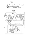
- the time intervals IT o each contain an incoming frame from the transmission medium.
- the transmission-reception end equipment in which the synchronization recovery device is included is in a phase of transmission of an outgoing frame.
- the incoming digital signal PE has consecutively throughout the duration of the intervals IT 1 a constant value, for example a zero value to which a logic state "0" corresponds.
- the time intervals IT 1 are hereinafter called empty time intervals.
- the empty time intervals IT 1 are used for synchronization.
- An empty interval IT 1 is associated with a determined pattern MF placed at the start of the frame of data bits succeeding the interval IT 1 , to constitute a synchronization word or frame alignment word MVT.
- the pattern MF comprises a first bit in state "1", that is to say a state complementary to state "0" corresponding to the empty intervals IT 1 .
- the MF pattern is for example made up of the binary combination "1110".
- the synchronization recovery device essentially comprises a shift register 1, a word comparator 2, a binary counter 3 and a frame alignment loss signaling circuit 4.
- Four parallel data outputs Q1 to Q4 of register 1 are respectively connected to the first four inputs of comparator 2.
- Comparator 2 outputs an EG signal in the "1" state when the 'MF pattern is detected in the PE signal.
- the binary counter 3 is a modulo L 1 -1536 counter.
- the counter 3 has the function of detecting the empty time intervals ITi in the signal PE. To this end, the counter 3 receives the rhythm signal Hb at a clock input CL and a reset signal RAZ at an initialization input R.
- An overflow indication signal DE in the state "1 " is supplied by counter 3 when a sequence of at least Li-1536 consecutive bits is detected in the PE signal.
- the reset signal PAZ is produced by an AND logic gate with two inputs 300 receiving the signal PE leaving register 1 and a complementary rhythm signal Hb.
- the signal Hb is produced by a logic inverter 301 from the rate signal Hb.
- Another two-input AND logic gate 302 is provided in the device in order to produce a frame alignment signal VT from the signals EG and DE.
- the loadings and offsets of the bits of the signal PE in the register 1 are controlled by states "1" of the rate signal Hb occurring during first half-periods of the signal Hb having a duration equal to 1 / (2.Fb).
- the reset of counter 3 is controlled by bits in state "1" of the signal PE contained in the time intervals IT 0 and this for second half-periods of the rate signal Hb corresponding to states "0" of said Hb signal.
- a "D" state is applied to a data entry D of the first flip-flop 400.
- the data inputs D of flip-flops 401 and 402 are connected respectively to data outputs Q of flip-flops 400 and 401.
- Reset inputs R of flip-flops 400 to 402 receive the pulses in state "1" of the signal of VT frame locking.
- a light-emitting diode 403 supplied by the PVT signal through a resistor 404 is provided in circuit 4 in order to produce a visual alarm in the event of loss of frame alignment.
Abstract
Description
La présente invention concerne de manière générale la synchronisation de signaux numériques dans des liaisons de communication. Plus particulièrement l'invention concerne la synchronisation de signaux numériques de paquets et de trames de paquets dans des liaisons de communication à l'alternat notamment par fibres optiques.The present invention relates generally to the synchronization of digital signals in communication links. More particularly, the invention relates to the synchronization of digital packet signals and packet frames in alternation communication links, in particular by optical fibers.
La transmission à l'alternat de signaux de communication est une solution intéressante pour des réseaux de télécommunications par fibres optiques. Cette solution autorise en effet l'utilisation d'une même fibre optique pour deux sens de transmission et pour plusieurs communications d'abonné et permet ainsi de rentabiliser au mieux la capacité très importante de la fibre.The transmission to the alternation of communication signals is an interesting solution for telecommunications networks by optical fibers. This solution in fact authorizes the use of the same optical fiber for two directions of transmission and for several subscriber communications and thus makes it possible to make the most of the very large capacity of the fiber.
Dans une communication à l'alternat, par exemple entre un central téléphonique et une installation d'abonné, la liaison entre le central et l'installation d'abonné n'est pas permanente et il est nécessaire de récupérer la synchronisation au début de chaque période de communication. Afin d'obtenir un bon confort d'écoute pour la communication, la récupération de la synchronisation appelée également récupération de verrouillage de trame dans les réseaux de télécommunications de type RNIS, doit être réalisée de manière extrêmement rapide, généralement en moins de 10 millisecondes.In an alternation communication, for example between a telephone exchange and a subscriber installation, the connection between the exchange and the subscriber installation is not permanent and it is necessary to recover synchronization at the start of each communication period. In order to obtain good listening comfort for communication, synchronization recovery, also called frame alignment recovery in ISDN type telecommunications networks, must be carried out extremely quickly, generally in less than 10 milliseconds.
Les dispositifs connus de récupération de verrouillage de trame sont généralement conçus pour des communications bidirectionnelles de type duplex. Dans ces dispositifs, le verrouillage de trame est déclaré acquis, à l'établissement d'une communication, après plusieurs réceptions successives d'un motif particulier de verrouillage de trame ce qui entraîne un temps de récupération du verrouillage de trame relativement important. De tels dispositifs sont donc inadaptés pour une récupération rapide du verrouillage de trame dans une communication à l'alternat.Known frame alignment recovery devices are generally designed for bidirectional communications of the duplex type. In these devices, the frame alignment is declared acquired, upon establishment of a communication, after several successive receptions of a particular pattern of frame alignment, which results in a relatively long recovery time for the frame alignment. Such devices are therefore unsuitable for rapid recovery of the frame alignment in a half-time communication.
La présente invention vise à fournir un procédé de synchronisation et des dispositifs de récupération de synchronisation destinés aux communications à l'alternat et tirant avantage d'une forme d'onde particulière des signaux de communication à l'alternat afin d'introduire dans lesdits signaux des mots de synchronisation de grande longueur à partir desquels une récupération de la synchronisation est obtenue très rapidement et avec une bonne fiabilité.The present invention aims to provide a synchronization method and synchronization recovery devices intended for alternation communications and taking advantage of a particular waveform of the alternation communication signals in order to introduce into said signals long synchronization words from which synchronization recovery is obtained very quickly and with good reliability.
A cette fin, le procédé selon l'invention pour synchroniser un signal de communication dans une liaison bidirectionnelle à l'alternat, ledit signal comprenant des premiers intervalles temporels occupés par des informations utiles et des seconds intervalles temporels vides d'informations utiles et à un premier état logique déterminé, est caractérisé en ce que
dans une extrémité de la liaison pour transmettre ledit signal dans la liaison, un motif numérique de synchronisation prédéterminé est inclus au début de chacun des premiers intervalles temporels, et en ce que dans une autre extrémité de la liaison pour recevoir ledit signal de la liaison, ledit motif est considéré comme associé aux seconds intervalles temporels, avec lesquels il constitue des mots de synchronisation qui sont détectés dans le signal de communication afin de récupérer la synchronisation du signal.To this end, the method according to the invention for synchronizing a communication signal in a bidirectional link to the half-board, said signal comprising first time intervals occupied by useful information and second time intervals empty with useful information and at a first determined logical state, is characterized in that
in one end of the link for transmitting said signal in the link, a predetermined digital synchronization pattern is included at the start of each of the first time intervals, and in that in another end of the link for receiving said signal from the link, said pattern is considered to be associated with the second time intervals, with which it constitutes synchronization words which are detected in the communication signal in order to recover the synchronization of the signal.
Un dispositif de récupération de synchronisation selon l'invention, inclus dans ladite autre extrémité recevant le signal, est caractérisé en ce qu'il comprend
des premiers moyens pour détecter dans le signal de communication, des séquences de bits au premier état logique ("0") de durée au moins égale à la durée des seconds intervalles temporels, des seconds moyens pour détecter le motif de synchronisation dans le signal de communication, et des moyens pour établir une impulsion de synchronisation lorsque ledit motif de synchronisation est détecté immédiatement après l'une desdites séquences de bits.A synchronization recovery device according to the invention, included in said other end receiving the signal, is characterized in that it comprises
first means for detecting in the communication signal, sequences of bits in the first logic state ("0") of duration at least equal to the duration of the second time intervals, second means for detecting the synchronization pattern in the signal communication, and means for establishing a synchronization pulse when said synchronization pattern is detected immediately after one of said bit sequences.
Selon une caractéristique de l'invention, le dispositif de récupération de synchronisation comprend également des moyens reliés aux moyens pour établir pour signaler une anomalie dans la synchronisation après un nombre prédéterminé de défauts de détection successifs du mot de synchronisation.According to a characteristic of the invention, the synchronization recovery device also comprises means connected to the means for establishing to signal an anomaly in synchronization after a predetermined number of successive detection faults of the synchronization word.
Selon l'invention le mot de synchronisation du fait de sa grande longueur est pratiquement inimitable et la synchronisation est récupérée avec une bonne fiabilité après une seule détection du mot de synchronisation.According to the invention, the synchronization word because of its great length is practically inimitable and the synchronization is recovered with good reliability after a single detection of the synchronization word.
D'autres avantages et caractéristiques de l'invention apparaîtront plus clairement à la lecture de la description suivante du procédé de synchronisation et de plusieurs réalisations préférées d'un dispositif de récupération de synchronisation selon l'invention en référence aux dessins annexés correspondants dans lesquels :
- - la Fig. 1 montre une forme d'onde d'un signal numérique de communication à l'alternat ; et
- - la Fig. 2 montre le schéma de principe d'un dispositif de récupération de synchronisation selon l'invention.
- - Fig. 1 shows a waveform of a digital alternation communication signal; and
- - Fig. 2 shows the block diagram of a synchronization recovery device according to the invention.
Dans un équipement d'extrémité de transmission-réception dans une liaison à l'alternat, un dispositif de récupération de synchronisation selon l'invention est situé en aval d'un dispositif de duplexage ayant un port bidirectionnel relié au support de transmission de la liaison, tel que fibre optique, pour transmettre et recevoir en alternat des signaux numériques tels par exemple que des paquets ou des trames numériques, une entrée recevant un signal numérique sortant par le port pour être transmis dans le support de transmission, et une sortie délivrant un signal numérique entrant par le port et en provenance du support de transmission.In a transmission-reception end device in a half-school link, a synchronization recovery device according to the invention is located downstream of a duplexing device having a bidirectional port connected to the transmission medium of the link. , such as optical fiber, for transmitting and receiving alternately digital signals such as for example digital packets or frames, an input receiving a digital signal leaving the port to be transmitted in the transmission medium, and an output delivering a digital signal entering through the port and coming from the transmission medium.
Il est considéré une transmission à l'alternat ayant par exemple une période de répétition TR=500 ils et une fréquence de transmission de bits Fb = 5,120 MHZ pour transmettre des trames numériques de longueur L= 1024 bits.It is considered a half-day transmission having for example a repetition period TR = 500 they and a bit transmission frequency Fb = 5.120 MHZ for transmitting digital frames of length L = 1024 bits.
En référence à la Fig. 1, le signal numérique entrant PE présente des premiers et seconds intervalles temporels alternés IT0 et IT1 respectivement de longueurs L= 1024 bits et Li = 1536 bits. La période de répétition TR correspond donc à une longueur de L+ L1 = 2560 = 5,120 x 500 bits. Les intervalles temporels ITo contiennent chacun une trame entrante en provenance du support de transmission. Pendant les intervalles temporels IT1, l'équipement d'extrémité de transmission-réception dans lequel est inclus le dispositif de récupération de synchronisation, est dans une phase de transmission d'une trame sortante. Le signal numérique entrant PE a consécutivement pendant toute la durée des intervalles IT1 une valeur constante, par exemple une valeur nulle à laquelle correspond un état logique "0". Les intervalles temporels IT1 sont appelés par la suite intervalles temporels vides. Les intervalles vides IT1 ont une longueur Li = 1536 bits supérieure à la longueur L= 1024 bits des intervalles temporels ITo du fait d'une durée de garde qui est prévue entre la fin de la transmission d'une trame sortante et la commutation du sens de communication pour la réception d'une trame entrante. Selon le procédé de l'invention, les intervalles temporels vides IT1 sont utilisés pour la synchronisation. Un intervalle vide IT1 est associé à un motif déterminé MF placé au début de la trame de bits de données succédant à l'intervalle IT1, pour constituer un mot de synchronisation ou mot de verrouillage de trame MVT. Le motif MF comprend un premier bit à l'état "1", soit à un état complémentaire à l'état "0" correspondant aux intervalles vides IT1. Le motif MF a une longueur relativement très faible par exemple égale à n=4 bits. Le motif MF est par exemple constitué de la combinaison binaire "1110".Au mot de verrouillage de trame MVT correspond donc la combinaison binaire "00....01110" comprenant une séquence de Li=1536 bits à l'état "0" suivie du motif MF="1110".With reference to FIG. 1, the incoming digital signal PE has first and second alternating time intervals IT 0 and IT 1, respectively of length L = 1024 bits and Li = 1536 bits. The repetition period TR therefore corresponds to a length of L + L 1 = 2560 = 5.120 x 500 bits. The time intervals IT o each contain an incoming frame from the transmission medium. During the time intervals IT 1 , the transmission-reception end equipment in which the synchronization recovery device is included, is in a phase of transmission of an outgoing frame. The incoming digital signal PE has consecutively throughout the duration of the intervals IT 1 a constant value, for example a zero value to which a logic state "0" corresponds. The time intervals IT 1 are hereinafter called empty time intervals. The empty intervals IT 1 have a length Li = 1536 bits greater than the length L = 1024 bits of the time intervals ITo due to a guard time which is provided between the end of the transmission of an outgoing frame and the switching of the communication direction for receiving an incoming frame. According to the method of the invention, the empty time intervals IT 1 are used for synchronization. An empty interval IT 1 is associated with a determined pattern MF placed at the start of the frame of data bits succeeding the interval IT 1 , to constitute a synchronization word or frame alignment word MVT. The pattern MF comprises a first bit in state "1", that is to say a state complementary to state "0" corresponding to the empty intervals IT 1 . The MF pattern has a relatively very short length, for example equal to n = 4 bits. The MF pattern is for example made up of the binary combination "1110". To the frame locking word MVT therefore corresponds the binary combination "00 .... 01110" comprising a sequence of Li = 1536 bits in the state "0" followed by the pattern MF = "1110".
En référence à la Fig. 2, le dispositif de récupération de synchronisation selon l'invention comprend essentiellement un registre à décalage 1, un comparateur de mots 2, un compteur binaire 3 et un circuit de signalisation de perte de verrouillage de trame 4. Le registre à décalage 1 comprend n=4 étages. Il reçoit le signal de paquet entrant PE à une entrée de données D et un signal de rythme de transmission de bits Hb de fréquence Fb = 5,120 Mhz à une entrée d'horloge CL. Quatre sorties parallèles de données Q1 à Q4 du registre 1 sont respectivement reliées à quatre premières entrées du comparateur 2. Une sortie série de données QS du registre 1 délivre le signal de paquet PE retardé de n=4 éléments binaires.With reference to FIG. 2, the synchronization recovery device according to the invention essentially comprises a
Le comparateur 2 a pour fonction de détecter dans le signal PE le motif MF="1110" lorsque celui-ci est chargé dans le registre à décalage 1. Quatre secondes entrées du comparateur 2 reçoivent respectivement les n=4 bits du motif MF qui sont mémorisés par exemple dans une mémoire morte câblée. Le comparateur 2 délivre en sortie un signal EG à l'état "1" lorsque le' motif MF est détecté dans le signal PE.The function of
Le compteur binaire 3 est un compteur modulo L1-1536. Le compteur 3 a pour fonction de déteccer les intervalles temporels vides ITi dans le signal PE. A cette fin, le compteur 3 reçoit le signal de rythme Hb à une entrée d'horloge CL et un signal de remise à zéro RAZ à une entrée d'initialisation R. Un signal d'indication de débordement DE à l'état "1" est fourni par le compteur 3 lorsqu'une séquence d'au moins Li-1536 bits consécutifs est détectée dans le signal PE.The
Le signal de remise à zéro PAZ est produit par une porte logique ET à deux entrées 300 recevant le signal PE sortant du registre 1 et un signal de rythme complémentaire Hb. Le signal Hb est produit par un inverseur logique 301 à partir du signal de rythme Hb.The reset signal PAZ is produced by an AND logic gate with two
Une autre porte logique ET à deux entrées 302 est prévue dans le dispositif afin de produire un signal de verrouillage de trame VT à partir des signaux EG et DE.Another two-input AND
Les chargements et décalages des bits du signal PE dans le registre 1 sont commandés par des états "1" du signal de rythme Hb intervenant pendant des premières demi-périodes du signal Hb ayant une durée égale à 1/(2.Fb). La remise à zéro du compteur 3 est commandée par des bits à l'état "1" du signal PE contenus dans les intervalles temporels IT0 et cela pendant des secondes demi-périodes du signal de rythme Hb correspondant à des états "0" dudit signal Hb.The loadings and offsets of the bits of the signal PE in the
Après la transmission par la sortie série QS du registre 1 du dernier bit des Li = 1536 bits à l'état "0" contenus dans un intervalle temporel vide IT1, le signal RAZ est resté à l'état inactif "0" pendant au moins une durée égale à IT1. Le compteur 3 a alors compté au moins Li = 1536 impulsions du signal de rythme Hb et est en débordement. Le signal DE est donc à l'état "1". Lorsque le premier bit à l'état "1" du motif MF= "1110" est fourni par la sortie série QS du registre 1, en réponse à un front montant du signal Hb, tous les bits du motif MF sont chargés dans le registre et le signal EG délivré par le comparateur 2 vient à l'état "1". Le signal de verrouillage de trame VT=DE.EG commute également à l'état "1". A l'issue d'une durée égale à 1/(2.Fb) après le transfert du premier bit du motif MF par la sortie série QS du registre 1 et la commutation du signal EG à l'état "1 ", le signal Hb vient à l'état "1 " et ouvre la porte 300. Le signal de remise à zéro RAZ commute consécutivement à l'état "1" et remet le compteur 3 à zéro. Le signal DE vient à l'état "0", la porte 302 se ferme, et le signal de verrouillage de trame VT revient à l'état "0". Une détection du mot de verrouillage de trame MVT dans le signal numérique entrant est donc signalée par une impulsion à l'état "1" de durée égale à 1/(2.Fb) apparaissant dans le signal VT.After the transmission via the QS serial output of
Le circuit de signalisation de perte de verrouillage de trame 4 a pour fonction de signaler une perte de verrouillage de trame après par exemple m=3 défauts de détection consécutifs du mot de verrouillage de trame MVT. Le circuit 4 comprend essentiellement m = 3 bascules analogues 400 à 402 connectées en cascade.The frame lock
Les m=3 bascules sont de préférence de type D. A une entrée de données D de la première bascule 400 est appliqué un état "1". Les entrées de données D des bascules 401 et 402 sont reliées respectivement à des sorties de données Q des bascules 400 et 401. Des entrées de remise à zéro R des bascules 400 à 402 reçoivent les impulsions à l'état "1" du signal de verrouillage de trame VT. Un signal de rythme de trame Ht de période Tt=TR=500 µs est appliqué à des entrées d'horloge CL des bascules 400 à 402.The m = 3 flip-flops are preferably of type D. A "D" state is applied to a data entry D of the first flip-
L'état "1" appliqué à l'entrée de données D de la bascule 400 ne traverse les m = 3 bascules 400 à 402 pour être délivré par la sortie de données Q de la bascule 402 et produire un signal de perte de verrouillage de trame PVT à l'état "1" qu'après au moins m=3 impulsions successives à l'état "1" manquantes dans le signal de verrouillage de trame VT, c'est-à-dire après au moins m=3 défauts de détection du mot de verrouillage de trame MVT. Une diode électroluminescente 403 alimentée par le signal PVT à travers une résistance 404 est prévue dans le circuit 4 afin de produire une alarme visuelle en cas de perte du verrouillage de trame.The state "1" applied to the data input D of the flip-
Claims (4)
Applications Claiming Priority (2)
| Application Number | Priority Date | Filing Date | Title |
|---|---|---|---|
| FR8811038 | 1988-08-19 | ||
| FR8811038A FR2635624B1 (en) | 1988-08-19 | 1988-08-19 | SYNCHRONIZATION METHOD AND SYNCHRONIZATION RECOVERY DEVICES FOR INTERNSHIP COMMUNICATIONS |
Publications (2)
| Publication Number | Publication Date |
|---|---|
| EP0355073A1 true EP0355073A1 (en) | 1990-02-21 |
| EP0355073B1 EP0355073B1 (en) | 1993-10-06 |
Family
ID=9369420
Family Applications (1)
| Application Number | Title | Priority Date | Filing Date |
|---|---|---|---|
| EP89402274A Expired - Lifetime EP0355073B1 (en) | 1988-08-19 | 1989-08-11 | Synchronisation method and synchronisation recovery circuits for time-shared communications |
Country Status (6)
| Country | Link |
|---|---|
| US (1) | US5046074A (en) |
| EP (1) | EP0355073B1 (en) |
| JP (1) | JP2995756B2 (en) |
| CA (1) | CA1338478C (en) |
| DE (1) | DE68909717T2 (en) |
| FR (1) | FR2635624B1 (en) |
Cited By (3)
| Publication number | Priority date | Publication date | Assignee | Title |
|---|---|---|---|---|
| EP0549154A2 (en) * | 1991-12-24 | 1993-06-30 | Advanced Micro Devices, Inc. | Repetitive pattern detection |
| EP0642242A2 (en) * | 1993-09-08 | 1995-03-08 | Alcatel Mobile Communication France | Data transmission frame with reduced ambiguity and a transmitter and receiver for such a frame |
| GB2293731A (en) * | 1993-09-07 | 1996-04-03 | Sagem | Detecting loss of synchronisation in a digital communication system |
Families Citing this family (7)
| Publication number | Priority date | Publication date | Assignee | Title |
|---|---|---|---|---|
| EP0447731B1 (en) * | 1990-03-13 | 1995-08-30 | International Business Machines Corporation | A synchronization circuit for a synchronous switching system |
| JPH04262630A (en) * | 1991-02-15 | 1992-09-18 | Fujitsu Ltd | Satellite communication system |
| FR2674393A1 (en) * | 1991-03-21 | 1992-09-25 | Bourgart Fabrice | SYNCHRONIZATION OF TERMINAL STATIONS IN AN ALTERNATE AND MULTIDEBIT NETWORK. |
| US5757869A (en) * | 1995-07-28 | 1998-05-26 | Adtran, Inc. | Apparatus and method for detecting frame synchronization pattern/word in bit-stuffed digital data frame |
| US6091785A (en) | 1997-09-25 | 2000-07-18 | Trimble Navigation Limited | Receiver having a memory based search for fast acquisition of a spread spectrum signal |
| DE10105794A1 (en) * | 2001-02-07 | 2002-08-08 | Philips Corp Intellectual Pty | Communication system, method and signal for time-coded data transmission |
| US10637535B1 (en) * | 2018-12-10 | 2020-04-28 | At&T Intellectual Property I, L.P. | Methods and apparatus to receive electromagnetic wave transmissions |
Citations (2)
| Publication number | Priority date | Publication date | Assignee | Title |
|---|---|---|---|---|
| US3959587A (en) * | 1972-07-07 | 1976-05-25 | Compagnie Industrielle Des Telecommunications Cit-Alcatel | Device for synchronizing a receiver of numerical data |
| US4002834A (en) * | 1974-12-09 | 1977-01-11 | The United States Of America As Represented By The Secretary Of The Navy | PCM synchronization and multiplexing system |
Family Cites Families (5)
| Publication number | Priority date | Publication date | Assignee | Title |
|---|---|---|---|---|
| US4611336A (en) * | 1984-02-21 | 1986-09-09 | Calculagraph Company | Frame synchronization for distributed framing pattern in electronic communication systems |
| US4679188A (en) * | 1984-09-26 | 1987-07-07 | Fujitsu Limited | Digital transmission system |
| CA1274928A (en) * | 1986-05-28 | 1990-10-02 | Hirotoshi Shirasu | Method and system for bidirectionally transmitting data |
| US4803703A (en) * | 1987-04-30 | 1989-02-07 | Motorola, Inc. | Apparatus and method for fine synchronization of a communication receiver |
| US4872186A (en) * | 1987-11-17 | 1989-10-03 | Honeywell Inc. | Apparatus and method for identification of message initiation in a process control network |
-
1988
- 1988-08-19 FR FR8811038A patent/FR2635624B1/en not_active Expired - Fee Related
-
1989
- 1989-08-11 EP EP89402274A patent/EP0355073B1/en not_active Expired - Lifetime
- 1989-08-11 DE DE89402274T patent/DE68909717T2/en not_active Expired - Fee Related
- 1989-08-16 US US07/394,322 patent/US5046074A/en not_active Expired - Lifetime
- 1989-08-17 CA CA000608614A patent/CA1338478C/en not_active Expired - Fee Related
- 1989-08-18 JP JP21157689A patent/JP2995756B2/en not_active Expired - Fee Related
Patent Citations (2)
| Publication number | Priority date | Publication date | Assignee | Title |
|---|---|---|---|---|
| US3959587A (en) * | 1972-07-07 | 1976-05-25 | Compagnie Industrielle Des Telecommunications Cit-Alcatel | Device for synchronizing a receiver of numerical data |
| US4002834A (en) * | 1974-12-09 | 1977-01-11 | The United States Of America As Represented By The Secretary Of The Navy | PCM synchronization and multiplexing system |
Cited By (7)
| Publication number | Priority date | Publication date | Assignee | Title |
|---|---|---|---|---|
| EP0549154A2 (en) * | 1991-12-24 | 1993-06-30 | Advanced Micro Devices, Inc. | Repetitive pattern detection |
| EP0549154A3 (en) * | 1991-12-24 | 1993-12-08 | Advanced Micro Devices Inc | Repetitive pattern detection |
| GB2293731A (en) * | 1993-09-07 | 1996-04-03 | Sagem | Detecting loss of synchronisation in a digital communication system |
| GB2293731B (en) * | 1993-09-07 | 1999-05-05 | Sagem | Method for the detection of a loss of synchronisation in a digital communication system and terminal for carrying out the method |
| EP0642242A2 (en) * | 1993-09-08 | 1995-03-08 | Alcatel Mobile Communication France | Data transmission frame with reduced ambiguity and a transmitter and receiver for such a frame |
| FR2709896A1 (en) * | 1993-09-08 | 1995-03-17 | Alcatel Mobile Comm France | Low ambiguity data transmission frame, transmitter and receiver adapted to such a frame. |
| EP0642242A3 (en) * | 1993-09-08 | 1995-05-10 | Alcatel Mobile Comm France | Data transmission frame with reduced ambiguity and a transmitter and receiver for such a frame. |
Also Published As
| Publication number | Publication date |
|---|---|
| EP0355073B1 (en) | 1993-10-06 |
| JPH02105649A (en) | 1990-04-18 |
| JP2995756B2 (en) | 1999-12-27 |
| FR2635624B1 (en) | 1994-05-13 |
| DE68909717T2 (en) | 1994-02-10 |
| FR2635624A1 (en) | 1990-02-23 |
| CA1338478C (en) | 1996-07-23 |
| DE68909717D1 (en) | 1993-11-11 |
| US5046074A (en) | 1991-09-03 |
Similar Documents
| Publication | Publication Date | Title |
|---|---|---|
| EP0113307B1 (en) | Alignment circuit for fixed-length digital information blocks | |
| EP0419337B1 (en) | Digital signal encoding method, encoder and decoder for carrying out the method, regeneration method and regenerator therefore | |
| EP0355073B1 (en) | Synchronisation method and synchronisation recovery circuits for time-shared communications | |
| FR2544570A1 (en) | APPARATUS FOR RECEIVING RAFALE SIGNALS | |
| FR2580130A1 (en) | ||
| EP0161177A1 (en) | Process and device for the recovery of a frame lock word with distributed bits within a digital signal | |
| EP0411529B1 (en) | Synchronous digital transmitter | |
| FR2687876A1 (en) | ERROR DETECTION ASSEMBLY FOR DIGITAL TRANSMISSION LINE AND MONITORING METHOD. | |
| EP0112429B1 (en) | System for the transmission of data by repetitive sequences | |
| EP0064923B1 (en) | System for the phase synchronization of digital data streams, and its application to the commutation of said data streams | |
| EP0112426B1 (en) | Synchronizing system for a multiplexed loop communication network | |
| EP0082054A1 (en) | Method of synchronising transceiver sets of a frequency-hopping network, and set for carrying out this method | |
| EP0396461B1 (en) | Device for synchronising a pseudo-binary signal with a phase-hopped regenerated clock signal | |
| CA1236552A (en) | Telesignalling method and device for a digital transmission link | |
| EP0161162A1 (en) | Automatic exchange with a video switching matrix | |
| EP0343083B1 (en) | Loss of synchronisation detection device, and its use in a digital transmission network | |
| EP0417681B1 (en) | Dual mode synchronisation device, in particular for the recovery of the frame-clock phase in a half-duplex transmission system | |
| FR2574202A1 (en) | METHOD AND DEVICE FOR TELESIGNALIZATION BY MESSAGE SUBSTITUTION TO DATA ACHIEVED BY A DIGITAL TRANSMISSION LINK | |
| EP0018618A1 (en) | Multiplex synchronisation device in a TDM exchange | |
| EP0394895B1 (en) | Communication adapter for remote control terminal | |
| FR2529415A1 (en) | Insertion unit for fibre=optic transmission system - converts HDB3 code signals into line code for error detection in regeneration unit at receiver side | |
| FR2661058A1 (en) | SIGNALING ASSEMBLY AND METHOD FOR MONITORING TELECOMMUNICATIONS REPEATERS. | |
| EP0540397B1 (en) | Method and circuit for counting clock-slips | |
| EP0660561B1 (en) | Circuit for recognition of a sequence of words in a modem | |
| CA2019774C (en) | Device for detecting in a binary signal a pointer consisting of a continuous sequence of binary elements having the same value |
Legal Events
| Date | Code | Title | Description |
|---|---|---|---|
| PUAI | Public reference made under article 153(3) epc to a published international application that has entered the european phase |
Free format text: ORIGINAL CODE: 0009012 |
|
| AK | Designated contracting states |
Kind code of ref document: A1 Designated state(s): DE GB IT NL SE |
|
| 17P | Request for examination filed |
Effective date: 19900118 |
|
| 17Q | First examination report despatched |
Effective date: 19920212 |
|
| RAP1 | Party data changed (applicant data changed or rights of an application transferred) |
Owner name: FRANCE TELECOM |
|
| GRAA | (expected) grant |
Free format text: ORIGINAL CODE: 0009210 |
|
| ITF | It: translation for a ep patent filed |
Owner name: ING. PIOVESANA PAOLO |
|
| AK | Designated contracting states |
Kind code of ref document: B1 Designated state(s): DE GB IT NL SE |
|
| REF | Corresponds to: |
Ref document number: 68909717 Country of ref document: DE Date of ref document: 19931111 |
|
| GBT | Gb: translation of ep patent filed (gb section 77(6)(a)/1977) |
Effective date: 19940112 |
|
| PLBE | No opposition filed within time limit |
Free format text: ORIGINAL CODE: 0009261 |
|
| STAA | Information on the status of an ep patent application or granted ep patent |
Free format text: STATUS: NO OPPOSITION FILED WITHIN TIME LIMIT |
|
| 26N | No opposition filed | ||
| EAL | Se: european patent in force in sweden |
Ref document number: 89402274.8 |
|
| REG | Reference to a national code |
Ref country code: GB Ref legal event code: IF02 |
|
| PGFP | Annual fee paid to national office [announced via postgrant information from national office to epo] |
Ref country code: GB Payment date: 20030725 Year of fee payment: 15 |
|
| PGFP | Annual fee paid to national office [announced via postgrant information from national office to epo] |
Ref country code: SE Payment date: 20030728 Year of fee payment: 15 Ref country code: NL Payment date: 20030728 Year of fee payment: 15 |
|
| PGFP | Annual fee paid to national office [announced via postgrant information from national office to epo] |
Ref country code: DE Payment date: 20030808 Year of fee payment: 15 |
|
| PG25 | Lapsed in a contracting state [announced via postgrant information from national office to epo] |
Ref country code: GB Free format text: LAPSE BECAUSE OF NON-PAYMENT OF DUE FEES Effective date: 20040811 |
|
| PG25 | Lapsed in a contracting state [announced via postgrant information from national office to epo] |
Ref country code: SE Free format text: LAPSE BECAUSE OF NON-PAYMENT OF DUE FEES Effective date: 20040812 |
|
| PG25 | Lapsed in a contracting state [announced via postgrant information from national office to epo] |
Ref country code: NL Free format text: LAPSE BECAUSE OF NON-PAYMENT OF DUE FEES Effective date: 20050301 Ref country code: DE Free format text: LAPSE BECAUSE OF NON-PAYMENT OF DUE FEES Effective date: 20050301 |
|
| EUG | Se: european patent has lapsed | ||
| GBPC | Gb: european patent ceased through non-payment of renewal fee |
Effective date: 20040811 |
|
| NLV4 | Nl: lapsed or anulled due to non-payment of the annual fee |
Effective date: 20050301 |
|
| PG25 | Lapsed in a contracting state [announced via postgrant information from national office to epo] |
Ref country code: IT Free format text: LAPSE BECAUSE OF NON-PAYMENT OF DUE FEES;WARNING: LAPSES OF ITALIAN PATENTS WITH EFFECTIVE DATE BEFORE 2007 MAY HAVE OCCURRED AT ANY TIME BEFORE 2007. THE CORRECT EFFECTIVE DATE MAY BE DIFFERENT FROM THE ONE RECORDED. Effective date: 20050811 |