EP0357064A2 - Metal bump type semiconductor device and method for manufacturing the same - Google Patents
Metal bump type semiconductor device and method for manufacturing the same Download PDFInfo
- Publication number
- EP0357064A2 EP0357064A2 EP19890116100 EP89116100A EP0357064A2 EP 0357064 A2 EP0357064 A2 EP 0357064A2 EP 19890116100 EP19890116100 EP 19890116100 EP 89116100 A EP89116100 A EP 89116100A EP 0357064 A2 EP0357064 A2 EP 0357064A2
- Authority
- EP
- European Patent Office
- Prior art keywords
- bump
- solder
- lead
- composition
- tin
- Prior art date
- Legal status (The legal status is an assumption and is not a legal conclusion. Google has not performed a legal analysis and makes no representation as to the accuracy of the status listed.)
- Granted
Links
Images
Classifications
-
- H—ELECTRICITY
- H01—ELECTRIC ELEMENTS
- H01L—SEMICONDUCTOR DEVICES NOT COVERED BY CLASS H10
- H01L23/00—Details of semiconductor or other solid state devices
- H01L23/52—Arrangements for conducting electric current within the device in operation from one component to another, i.e. interconnections, e.g. wires, lead frames
- H01L23/522—Arrangements for conducting electric current within the device in operation from one component to another, i.e. interconnections, e.g. wires, lead frames including external interconnections consisting of a multilayer structure of conductive and insulating layers inseparably formed on the semiconductor body
- H01L23/532—Arrangements for conducting electric current within the device in operation from one component to another, i.e. interconnections, e.g. wires, lead frames including external interconnections consisting of a multilayer structure of conductive and insulating layers inseparably formed on the semiconductor body characterised by the materials
- H01L23/53204—Conductive materials
- H01L23/53209—Conductive materials based on metals, e.g. alloys, metal silicides
-
- H—ELECTRICITY
- H01—ELECTRIC ELEMENTS
- H01L—SEMICONDUCTOR DEVICES NOT COVERED BY CLASS H10
- H01L23/00—Details of semiconductor or other solid state devices
- H01L23/48—Arrangements for conducting electric current to or from the solid state body in operation, e.g. leads, terminal arrangements ; Selection of materials therefor
-
- H—ELECTRICITY
- H01—ELECTRIC ELEMENTS
- H01L—SEMICONDUCTOR DEVICES NOT COVERED BY CLASS H10
- H01L24/00—Arrangements for connecting or disconnecting semiconductor or solid-state bodies; Methods or apparatus related thereto
- H01L24/01—Means for bonding being attached to, or being formed on, the surface to be connected, e.g. chip-to-package, die-attach, "first-level" interconnects; Manufacturing methods related thereto
- H01L24/10—Bump connectors ; Manufacturing methods related thereto
-
- H—ELECTRICITY
- H01—ELECTRIC ELEMENTS
- H01L—SEMICONDUCTOR DEVICES NOT COVERED BY CLASS H10
- H01L24/00—Arrangements for connecting or disconnecting semiconductor or solid-state bodies; Methods or apparatus related thereto
- H01L24/01—Means for bonding being attached to, or being formed on, the surface to be connected, e.g. chip-to-package, die-attach, "first-level" interconnects; Manufacturing methods related thereto
- H01L24/02—Bonding areas ; Manufacturing methods related thereto
-
- H—ELECTRICITY
- H01—ELECTRIC ELEMENTS
- H01L—SEMICONDUCTOR DEVICES NOT COVERED BY CLASS H10
- H01L24/00—Arrangements for connecting or disconnecting semiconductor or solid-state bodies; Methods or apparatus related thereto
- H01L24/01—Means for bonding being attached to, or being formed on, the surface to be connected, e.g. chip-to-package, die-attach, "first-level" interconnects; Manufacturing methods related thereto
- H01L24/10—Bump connectors ; Manufacturing methods related thereto
- H01L24/12—Structure, shape, material or disposition of the bump connectors prior to the connecting process
- H01L24/13—Structure, shape, material or disposition of the bump connectors prior to the connecting process of an individual bump connector
-
- H—ELECTRICITY
- H01—ELECTRIC ELEMENTS
- H01L—SEMICONDUCTOR DEVICES NOT COVERED BY CLASS H10
- H01L2224/00—Indexing scheme for arrangements for connecting or disconnecting semiconductor or solid-state bodies and methods related thereto as covered by H01L24/00
- H01L2224/01—Means for bonding being attached to, or being formed on, the surface to be connected, e.g. chip-to-package, die-attach, "first-level" interconnects; Manufacturing methods related thereto
- H01L2224/02—Bonding areas; Manufacturing methods related thereto
- H01L2224/04—Structure, shape, material or disposition of the bonding areas prior to the connecting process
- H01L2224/0401—Bonding areas specifically adapted for bump connectors, e.g. under bump metallisation [UBM]
-
- H—ELECTRICITY
- H01—ELECTRIC ELEMENTS
- H01L—SEMICONDUCTOR DEVICES NOT COVERED BY CLASS H10
- H01L2224/00—Indexing scheme for arrangements for connecting or disconnecting semiconductor or solid-state bodies and methods related thereto as covered by H01L24/00
- H01L2224/01—Means for bonding being attached to, or being formed on, the surface to be connected, e.g. chip-to-package, die-attach, "first-level" interconnects; Manufacturing methods related thereto
- H01L2224/02—Bonding areas; Manufacturing methods related thereto
- H01L2224/04—Structure, shape, material or disposition of the bonding areas prior to the connecting process
- H01L2224/05—Structure, shape, material or disposition of the bonding areas prior to the connecting process of an individual bonding area
- H01L2224/0554—External layer
- H01L2224/05541—Structure
- H01L2224/05548—Bonding area integrally formed with a redistribution layer on the semiconductor or solid-state body
-
- H—ELECTRICITY
- H01—ELECTRIC ELEMENTS
- H01L—SEMICONDUCTOR DEVICES NOT COVERED BY CLASS H10
- H01L2224/00—Indexing scheme for arrangements for connecting or disconnecting semiconductor or solid-state bodies and methods related thereto as covered by H01L24/00
- H01L2224/01—Means for bonding being attached to, or being formed on, the surface to be connected, e.g. chip-to-package, die-attach, "first-level" interconnects; Manufacturing methods related thereto
- H01L2224/02—Bonding areas; Manufacturing methods related thereto
- H01L2224/04—Structure, shape, material or disposition of the bonding areas prior to the connecting process
- H01L2224/05—Structure, shape, material or disposition of the bonding areas prior to the connecting process of an individual bonding area
- H01L2224/0554—External layer
- H01L2224/0556—Disposition
- H01L2224/05567—Disposition the external layer being at least partially embedded in the surface
-
- H—ELECTRICITY
- H01—ELECTRIC ELEMENTS
- H01L—SEMICONDUCTOR DEVICES NOT COVERED BY CLASS H10
- H01L2224/00—Indexing scheme for arrangements for connecting or disconnecting semiconductor or solid-state bodies and methods related thereto as covered by H01L24/00
- H01L2224/01—Means for bonding being attached to, or being formed on, the surface to be connected, e.g. chip-to-package, die-attach, "first-level" interconnects; Manufacturing methods related thereto
- H01L2224/02—Bonding areas; Manufacturing methods related thereto
- H01L2224/04—Structure, shape, material or disposition of the bonding areas prior to the connecting process
- H01L2224/05—Structure, shape, material or disposition of the bonding areas prior to the connecting process of an individual bonding area
- H01L2224/0554—External layer
- H01L2224/05599—Material
- H01L2224/056—Material with a principal constituent of the material being a metal or a metalloid, e.g. boron [B], silicon [Si], germanium [Ge], arsenic [As], antimony [Sb], tellurium [Te] and polonium [Po], and alloys thereof
- H01L2224/05617—Material with a principal constituent of the material being a metal or a metalloid, e.g. boron [B], silicon [Si], germanium [Ge], arsenic [As], antimony [Sb], tellurium [Te] and polonium [Po], and alloys thereof the principal constituent melting at a temperature of greater than or equal to 400°C and less than 950°C
- H01L2224/05624—Aluminium [Al] as principal constituent
-
- H—ELECTRICITY
- H01—ELECTRIC ELEMENTS
- H01L—SEMICONDUCTOR DEVICES NOT COVERED BY CLASS H10
- H01L2224/00—Indexing scheme for arrangements for connecting or disconnecting semiconductor or solid-state bodies and methods related thereto as covered by H01L24/00
- H01L2224/01—Means for bonding being attached to, or being formed on, the surface to be connected, e.g. chip-to-package, die-attach, "first-level" interconnects; Manufacturing methods related thereto
- H01L2224/10—Bump connectors; Manufacturing methods related thereto
- H01L2224/12—Structure, shape, material or disposition of the bump connectors prior to the connecting process
- H01L2224/13—Structure, shape, material or disposition of the bump connectors prior to the connecting process of an individual bump connector
- H01L2224/13001—Core members of the bump connector
- H01L2224/13005—Structure
- H01L2224/13007—Bump connector smaller than the underlying bonding area, e.g. than the under bump metallisation [UBM]
-
- H—ELECTRICITY
- H01—ELECTRIC ELEMENTS
- H01L—SEMICONDUCTOR DEVICES NOT COVERED BY CLASS H10
- H01L2224/00—Indexing scheme for arrangements for connecting or disconnecting semiconductor or solid-state bodies and methods related thereto as covered by H01L24/00
- H01L2224/01—Means for bonding being attached to, or being formed on, the surface to be connected, e.g. chip-to-package, die-attach, "first-level" interconnects; Manufacturing methods related thereto
- H01L2224/10—Bump connectors; Manufacturing methods related thereto
- H01L2224/12—Structure, shape, material or disposition of the bump connectors prior to the connecting process
- H01L2224/13—Structure, shape, material or disposition of the bump connectors prior to the connecting process of an individual bump connector
- H01L2224/13001—Core members of the bump connector
- H01L2224/1302—Disposition
- H01L2224/13022—Disposition the bump connector being at least partially embedded in the surface
-
- H—ELECTRICITY
- H01—ELECTRIC ELEMENTS
- H01L—SEMICONDUCTOR DEVICES NOT COVERED BY CLASS H10
- H01L2224/00—Indexing scheme for arrangements for connecting or disconnecting semiconductor or solid-state bodies and methods related thereto as covered by H01L24/00
- H01L2224/01—Means for bonding being attached to, or being formed on, the surface to be connected, e.g. chip-to-package, die-attach, "first-level" interconnects; Manufacturing methods related thereto
- H01L2224/10—Bump connectors; Manufacturing methods related thereto
- H01L2224/12—Structure, shape, material or disposition of the bump connectors prior to the connecting process
- H01L2224/13—Structure, shape, material or disposition of the bump connectors prior to the connecting process of an individual bump connector
- H01L2224/13001—Core members of the bump connector
- H01L2224/13099—Material
-
- H—ELECTRICITY
- H01—ELECTRIC ELEMENTS
- H01L—SEMICONDUCTOR DEVICES NOT COVERED BY CLASS H10
- H01L2224/00—Indexing scheme for arrangements for connecting or disconnecting semiconductor or solid-state bodies and methods related thereto as covered by H01L24/00
- H01L2224/01—Means for bonding being attached to, or being formed on, the surface to be connected, e.g. chip-to-package, die-attach, "first-level" interconnects; Manufacturing methods related thereto
- H01L2224/42—Wire connectors; Manufacturing methods related thereto
- H01L2224/44—Structure, shape, material or disposition of the wire connectors prior to the connecting process
- H01L2224/45—Structure, shape, material or disposition of the wire connectors prior to the connecting process of an individual wire connector
- H01L2224/45001—Core members of the connector
- H01L2224/45099—Material
- H01L2224/451—Material with a principal constituent of the material being a metal or a metalloid, e.g. boron (B), silicon (Si), germanium (Ge), arsenic (As), antimony (Sb), tellurium (Te) and polonium (Po), and alloys thereof
- H01L2224/45117—Material with a principal constituent of the material being a metal or a metalloid, e.g. boron (B), silicon (Si), germanium (Ge), arsenic (As), antimony (Sb), tellurium (Te) and polonium (Po), and alloys thereof the principal constituent melting at a temperature of greater than or equal to 400°C and less than 950°C
- H01L2224/45124—Aluminium (Al) as principal constituent
-
- H—ELECTRICITY
- H01—ELECTRIC ELEMENTS
- H01L—SEMICONDUCTOR DEVICES NOT COVERED BY CLASS H10
- H01L24/00—Arrangements for connecting or disconnecting semiconductor or solid-state bodies; Methods or apparatus related thereto
- H01L24/01—Means for bonding being attached to, or being formed on, the surface to be connected, e.g. chip-to-package, die-attach, "first-level" interconnects; Manufacturing methods related thereto
- H01L24/02—Bonding areas ; Manufacturing methods related thereto
- H01L24/03—Manufacturing methods
-
- H—ELECTRICITY
- H01—ELECTRIC ELEMENTS
- H01L—SEMICONDUCTOR DEVICES NOT COVERED BY CLASS H10
- H01L24/00—Arrangements for connecting or disconnecting semiconductor or solid-state bodies; Methods or apparatus related thereto
- H01L24/01—Means for bonding being attached to, or being formed on, the surface to be connected, e.g. chip-to-package, die-attach, "first-level" interconnects; Manufacturing methods related thereto
- H01L24/02—Bonding areas ; Manufacturing methods related thereto
- H01L24/04—Structure, shape, material or disposition of the bonding areas prior to the connecting process
- H01L24/05—Structure, shape, material or disposition of the bonding areas prior to the connecting process of an individual bonding area
-
- H—ELECTRICITY
- H01—ELECTRIC ELEMENTS
- H01L—SEMICONDUCTOR DEVICES NOT COVERED BY CLASS H10
- H01L24/00—Arrangements for connecting or disconnecting semiconductor or solid-state bodies; Methods or apparatus related thereto
- H01L24/01—Means for bonding being attached to, or being formed on, the surface to be connected, e.g. chip-to-package, die-attach, "first-level" interconnects; Manufacturing methods related thereto
- H01L24/10—Bump connectors ; Manufacturing methods related thereto
- H01L24/11—Manufacturing methods
-
- H—ELECTRICITY
- H01—ELECTRIC ELEMENTS
- H01L—SEMICONDUCTOR DEVICES NOT COVERED BY CLASS H10
- H01L2924/00—Indexing scheme for arrangements or methods for connecting or disconnecting semiconductor or solid-state bodies as covered by H01L24/00
- H01L2924/0001—Technical content checked by a classifier
- H01L2924/00014—Technical content checked by a classifier the subject-matter covered by the group, the symbol of which is combined with the symbol of this group, being disclosed without further technical details
-
- H—ELECTRICITY
- H01—ELECTRIC ELEMENTS
- H01L—SEMICONDUCTOR DEVICES NOT COVERED BY CLASS H10
- H01L2924/00—Indexing scheme for arrangements or methods for connecting or disconnecting semiconductor or solid-state bodies as covered by H01L24/00
- H01L2924/01—Chemical elements
- H01L2924/01006—Carbon [C]
-
- H—ELECTRICITY
- H01—ELECTRIC ELEMENTS
- H01L—SEMICONDUCTOR DEVICES NOT COVERED BY CLASS H10
- H01L2924/00—Indexing scheme for arrangements or methods for connecting or disconnecting semiconductor or solid-state bodies as covered by H01L24/00
- H01L2924/01—Chemical elements
- H01L2924/01013—Aluminum [Al]
-
- H—ELECTRICITY
- H01—ELECTRIC ELEMENTS
- H01L—SEMICONDUCTOR DEVICES NOT COVERED BY CLASS H10
- H01L2924/00—Indexing scheme for arrangements or methods for connecting or disconnecting semiconductor or solid-state bodies as covered by H01L24/00
- H01L2924/01—Chemical elements
- H01L2924/01018—Argon [Ar]
-
- H—ELECTRICITY
- H01—ELECTRIC ELEMENTS
- H01L—SEMICONDUCTOR DEVICES NOT COVERED BY CLASS H10
- H01L2924/00—Indexing scheme for arrangements or methods for connecting or disconnecting semiconductor or solid-state bodies as covered by H01L24/00
- H01L2924/01—Chemical elements
- H01L2924/0102—Calcium [Ca]
-
- H—ELECTRICITY
- H01—ELECTRIC ELEMENTS
- H01L—SEMICONDUCTOR DEVICES NOT COVERED BY CLASS H10
- H01L2924/00—Indexing scheme for arrangements or methods for connecting or disconnecting semiconductor or solid-state bodies as covered by H01L24/00
- H01L2924/01—Chemical elements
- H01L2924/01022—Titanium [Ti]
-
- H—ELECTRICITY
- H01—ELECTRIC ELEMENTS
- H01L—SEMICONDUCTOR DEVICES NOT COVERED BY CLASS H10
- H01L2924/00—Indexing scheme for arrangements or methods for connecting or disconnecting semiconductor or solid-state bodies as covered by H01L24/00
- H01L2924/01—Chemical elements
- H01L2924/01024—Chromium [Cr]
-
- H—ELECTRICITY
- H01—ELECTRIC ELEMENTS
- H01L—SEMICONDUCTOR DEVICES NOT COVERED BY CLASS H10
- H01L2924/00—Indexing scheme for arrangements or methods for connecting or disconnecting semiconductor or solid-state bodies as covered by H01L24/00
- H01L2924/01—Chemical elements
- H01L2924/01029—Copper [Cu]
-
- H—ELECTRICITY
- H01—ELECTRIC ELEMENTS
- H01L—SEMICONDUCTOR DEVICES NOT COVERED BY CLASS H10
- H01L2924/00—Indexing scheme for arrangements or methods for connecting or disconnecting semiconductor or solid-state bodies as covered by H01L24/00
- H01L2924/01—Chemical elements
- H01L2924/0103—Zinc [Zn]
-
- H—ELECTRICITY
- H01—ELECTRIC ELEMENTS
- H01L—SEMICONDUCTOR DEVICES NOT COVERED BY CLASS H10
- H01L2924/00—Indexing scheme for arrangements or methods for connecting or disconnecting semiconductor or solid-state bodies as covered by H01L24/00
- H01L2924/01—Chemical elements
- H01L2924/01033—Arsenic [As]
-
- H—ELECTRICITY
- H01—ELECTRIC ELEMENTS
- H01L—SEMICONDUCTOR DEVICES NOT COVERED BY CLASS H10
- H01L2924/00—Indexing scheme for arrangements or methods for connecting or disconnecting semiconductor or solid-state bodies as covered by H01L24/00
- H01L2924/01—Chemical elements
- H01L2924/01042—Molybdenum [Mo]
-
- H—ELECTRICITY
- H01—ELECTRIC ELEMENTS
- H01L—SEMICONDUCTOR DEVICES NOT COVERED BY CLASS H10
- H01L2924/00—Indexing scheme for arrangements or methods for connecting or disconnecting semiconductor or solid-state bodies as covered by H01L24/00
- H01L2924/01—Chemical elements
- H01L2924/01047—Silver [Ag]
-
- H—ELECTRICITY
- H01—ELECTRIC ELEMENTS
- H01L—SEMICONDUCTOR DEVICES NOT COVERED BY CLASS H10
- H01L2924/00—Indexing scheme for arrangements or methods for connecting or disconnecting semiconductor or solid-state bodies as covered by H01L24/00
- H01L2924/01—Chemical elements
- H01L2924/01074—Tungsten [W]
-
- H—ELECTRICITY
- H01—ELECTRIC ELEMENTS
- H01L—SEMICONDUCTOR DEVICES NOT COVERED BY CLASS H10
- H01L2924/00—Indexing scheme for arrangements or methods for connecting or disconnecting semiconductor or solid-state bodies as covered by H01L24/00
- H01L2924/01—Chemical elements
- H01L2924/01075—Rhenium [Re]
-
- H—ELECTRICITY
- H01—ELECTRIC ELEMENTS
- H01L—SEMICONDUCTOR DEVICES NOT COVERED BY CLASS H10
- H01L2924/00—Indexing scheme for arrangements or methods for connecting or disconnecting semiconductor or solid-state bodies as covered by H01L24/00
- H01L2924/01—Chemical elements
- H01L2924/01078—Platinum [Pt]
-
- H—ELECTRICITY
- H01—ELECTRIC ELEMENTS
- H01L—SEMICONDUCTOR DEVICES NOT COVERED BY CLASS H10
- H01L2924/00—Indexing scheme for arrangements or methods for connecting or disconnecting semiconductor or solid-state bodies as covered by H01L24/00
- H01L2924/01—Chemical elements
- H01L2924/01079—Gold [Au]
-
- H—ELECTRICITY
- H01—ELECTRIC ELEMENTS
- H01L—SEMICONDUCTOR DEVICES NOT COVERED BY CLASS H10
- H01L2924/00—Indexing scheme for arrangements or methods for connecting or disconnecting semiconductor or solid-state bodies as covered by H01L24/00
- H01L2924/01—Chemical elements
- H01L2924/01082—Lead [Pb]
-
- H—ELECTRICITY
- H01—ELECTRIC ELEMENTS
- H01L—SEMICONDUCTOR DEVICES NOT COVERED BY CLASS H10
- H01L2924/00—Indexing scheme for arrangements or methods for connecting or disconnecting semiconductor or solid-state bodies as covered by H01L24/00
- H01L2924/013—Alloys
- H01L2924/0132—Binary Alloys
- H01L2924/01322—Eutectic Alloys, i.e. obtained by a liquid transforming into two solid phases
-
- H—ELECTRICITY
- H01—ELECTRIC ELEMENTS
- H01L—SEMICONDUCTOR DEVICES NOT COVERED BY CLASS H10
- H01L2924/00—Indexing scheme for arrangements or methods for connecting or disconnecting semiconductor or solid-state bodies as covered by H01L24/00
- H01L2924/013—Alloys
- H01L2924/014—Solder alloys
-
- H—ELECTRICITY
- H01—ELECTRIC ELEMENTS
- H01L—SEMICONDUCTOR DEVICES NOT COVERED BY CLASS H10
- H01L2924/00—Indexing scheme for arrangements or methods for connecting or disconnecting semiconductor or solid-state bodies as covered by H01L24/00
- H01L2924/10—Details of semiconductor or other solid state devices to be connected
- H01L2924/102—Material of the semiconductor or solid state bodies
- H01L2924/1025—Semiconducting materials
- H01L2924/10251—Elemental semiconductors, i.e. Group IV
- H01L2924/10253—Silicon [Si]
-
- H—ELECTRICITY
- H01—ELECTRIC ELEMENTS
- H01L—SEMICONDUCTOR DEVICES NOT COVERED BY CLASS H10
- H01L2924/00—Indexing scheme for arrangements or methods for connecting or disconnecting semiconductor or solid-state bodies as covered by H01L24/00
- H01L2924/10—Details of semiconductor or other solid state devices to be connected
- H01L2924/11—Device type
- H01L2924/13—Discrete devices, e.g. 3 terminal devices
- H01L2924/1301—Thyristor
-
- H—ELECTRICITY
- H01—ELECTRIC ELEMENTS
- H01L—SEMICONDUCTOR DEVICES NOT COVERED BY CLASS H10
- H01L2924/00—Indexing scheme for arrangements or methods for connecting or disconnecting semiconductor or solid-state bodies as covered by H01L24/00
- H01L2924/10—Details of semiconductor or other solid state devices to be connected
- H01L2924/11—Device type
- H01L2924/13—Discrete devices, e.g. 3 terminal devices
- H01L2924/1304—Transistor
- H01L2924/1305—Bipolar Junction Transistor [BJT]
-
- H—ELECTRICITY
- H01—ELECTRIC ELEMENTS
- H01L—SEMICONDUCTOR DEVICES NOT COVERED BY CLASS H10
- H01L2924/00—Indexing scheme for arrangements or methods for connecting or disconnecting semiconductor or solid-state bodies as covered by H01L24/00
- H01L2924/15—Details of package parts other than the semiconductor or other solid state devices to be connected
- H01L2924/151—Die mounting substrate
- H01L2924/156—Material
- H01L2924/15786—Material with a principal constituent of the material being a non metallic, non metalloid inorganic material
- H01L2924/15787—Ceramics, e.g. crystalline carbides, nitrides or oxides
-
- Y—GENERAL TAGGING OF NEW TECHNOLOGICAL DEVELOPMENTS; GENERAL TAGGING OF CROSS-SECTIONAL TECHNOLOGIES SPANNING OVER SEVERAL SECTIONS OF THE IPC; TECHNICAL SUBJECTS COVERED BY FORMER USPC CROSS-REFERENCE ART COLLECTIONS [XRACs] AND DIGESTS
- Y10—TECHNICAL SUBJECTS COVERED BY FORMER USPC
- Y10S—TECHNICAL SUBJECTS COVERED BY FORMER USPC CROSS-REFERENCE ART COLLECTIONS [XRACs] AND DIGESTS
- Y10S438/00—Semiconductor device manufacturing: process
- Y10S438/928—Front and rear surface processing
Abstract
Description
- This invention relates to a semiconductor device having a metal bump formed therein and a method for manufacturing the same, and more particularly to a metal bump type semiconductor device having a metal bump formed directly on an electrode wiring pattern of Aℓ or Aℓ alloy without using a backing metal layer and a method for manufacturing the same.
- Various wireless bonding techniques for the semiconductor device such as a tape automated bonding (TAB) method, flip-chip method and controlled collapse bonding (CCB) method are known. With these methods, a metal bump formed of Au, solder or the like is generally formed on the electrode of the semiconductor chip and a metal connector or inner lead wire is connected to the metal bump to lead out the electrode of the semiconductor element formed on the chip to the exterior. Pb-Sn (solder) which is inexpensive is frequently used as material of the metal bump.
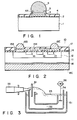
- Fig. 1 shows portion of the prior art semiconductor device including a bump of Pb-Sn. That is,
insulation film 2 of SiO₂, for example is formed on silicon substrate 1 andelectrode wiring pattern 3 of Aℓ or Aℓ alloy (which is simply referred to as an Aℓ electrode) is formed oninsulation film 2.Passivation insulation film 4 formed of SiN film or the like is formed oninsulation film 2 andAℓ electrode 3 to cover the same.Opening 4A is formed in that portion ofpassivation insulation film 4 which lies onAℓ electrode 3 so as to expose part of the surface ofAℓ electrode 3. Backingmetal layer 5 formed of Cr, Ni, Mo, Cu, Au, Ag or the like is formed on the exposed surface ofAℓ electrode 3. Solder bump 6 is formed onbacking metal layer 5 by plating or vapor deposition. - As described above, in the conventional semiconductor device having solder bump 6 formed on
Aℓ electrode 3 and a method for manufacturing the same, it is necessary to disposebacking metal layer 5 betweenAℓ electrode 3 and solder bump 6 in order to improve the bonding property betweenAℓ electrode 3 and solder bump 6. Further, it is necessary to form a mask so as not to plate or vapor deposit solder on portion other than the electrode portion when solder bump 6 is formed. As a result, the manufacturing process becomes complicated. - In order to solve the above problem, a method of forming a solder bump directly on the Aℓ electrode without using a backing metal plate has been proposed and disclosed in Japanese Patent Disclosure No. 62-104143 made by the same applicant as that of this application. The method disclosed in the above Japanese Patent Disclosure is to form a solder bump by applying ultrasonic waves to molten solder so as to break a natural oxide film formed on the surface of the electrode of Aℓ or Aℓ alloy, for example. This method has received much attention as a wireless bonding method for the semiconductor device.
- The principle of the method disclosed in the above Patent Disclosure is as follows: That is, when ultrasonic waves are applied to the molten solder with the molten solder kept in contact with the electrode portion of Aℓ, Aℓ alloy or the like, vaporized metal bubbles occur in the molten solder in the rarefaction or suction phase of the ultrasonic waves and the bubbles will be crushed and disappear in the next compression phase. When the compressed bubbles are destroyed, a strong shock is given to the surface of the Aℓ electrode so that the natural oxide film formed on the Aℓ electrode can be broken and at the same time solder is bonded to the newly created and exposed surface of the Aℓ electrode. In this way, a solder bump is formed directly on the Aℓ electrode without using a backing metal layer.
- As a specific method, a wafer is dipped into molten solder in a solder bath and an ultrasonic transducer is inserted into the molten solder to apply ultrasonic waves to the molten solder. Alternatively, ultrasonic waves can be applied to the molten solder by vibrating the solder bath in an ultrasonic mode. Further, ultrasonic waves can be applied to the molten solder while the molten solder is set in contact with the Aℓ electrode by using a soldering iron which can be vibrated in an ultrasonic mode. All the above-described methods are hereinafter referred to as an ultrasonic soldering method. It is generally understood that a solder bump can be formed directly on Aℓ or Aℓ alloy by the ultrasonic soldering method by using solder containing Sn as solder composition.
- The above method is simple, but has the following basic problem because Sn-series solder is used and is not yet generally used in the field of a semiconductor industry, for example. The first problem is related to formation of an Aℓ-Sn alloy layer and the second problem is related to absorption phenomenon of the base metal of Aℓ or Aℓ alloy caused by the presence of molten solder. The problems are explained in detail.
- First, the first problem is explained. For example, in a case where a Pb-Sn eutectic alloy is used as the Sn-series solder and a solder bump is formed directly on an Aℓ electrode, an Aℓ-Sn alloy layer is formed between the Aℓ electrode and the solder bump. A potential difference occurs between the Aℓ-Sn alloy layer and the Aℓ electrode to form a parasitic battery cell (or eutectic battery cell), thereby corroding the Aℓ electrode. The Aℓ-Sn alloy layer further grows when held at high temperatures (higher than 100°C), further corroding the Aℓ electrode and significantly degrading the bonding property of the junction between the solder and Aℓ. In particular, when the solder bump is melted so as to be connected to a metal connector or inner lead for electrode lead-out, for example, after the solder bump is formed, the above alloy layer grows larger irrespective of the Pb-Sn composition ratio of the solder, significantly degrading the bonding property of the junction between the solder and Aℓ.
- Next, the second problem is explained. When the molten solder is set in contact with Aℓ, a so-called absorption phenomenon in which Aℓ is melted or absorbed into the solder occurs and proceeds at a relatively high speed irrespective of the Pb-Sn composition ratio. Since the processing time for forming the solder bump by the ultrasonic soldering method can be made shorter than several seconds, influence by the absorption action of Aℓ can be suppressed as small as negligible. However, when the solder is melted again to connect the bump to an inner lead or the like in the later step and if it is held at high temperatures for more than several tens of seconds, the absorption action of Aℓ may proceed significantly. As a result, portion of Aℓ except the electrode portion on which the bump is formed is eaten by or absorbed into the solder, making it extremely difficult to selectively and precisely form the bump. Further, a top passivation film formed of SiN, for example, for chip protection is generally formed on the top layer of the semiconductor chip. If the SiN film is formed on the Aℓ electrode, the solder bump can be formed with the SiN film used as a block film. At this time, if the absorption action proceeds and the solder penetrates into portion of the Aℓ electrode under the SiN film, the SiN film may crack and cannot have a protection function as a passivation film.
- As described above, in the conventional technique in which the solder bump is formed on the electrode wiring pattern containing Aℓ as a main part through the backing metal layer, the manufacturing process becomes complicated and the productivity is lowered. It is possible to form the solder bump directly on the Aℓ electrode by use of the ultrasonic soldering method using Sn-series solder. However, in this case, an Aℓ-Sn alloy layer is formed and the absorption phenomenon of Aℓ will occur. In particular, if the structure is placed under a high temperature condition in the step of connecting a metal connector or inner lead after the bump is formed, the Aℓ-Sn alloy layer further grows and the absorption action further proceeds. As a result, the reliability of the semiconductor device is degraded.
- In order to solve the above problems, the inventors made various experiments by ultrasonic soldering methods using solder containing Ag in addition to Pb-Sn. The presence of Ag caused
Ag ₃ Aℓ (Ag ₂ Aℓ) to be formed and prevented formation of an Aℓ-Sn alloy layer. However, it was confirmed that the Ag-Aℓ alloy layer was weak, and like the Aℓ-Sn alloy layer, the weak Ag-Sn alloy layer will grow when the solder bump is melted again, thus making it impossible to attain a sufficiently high bonding strength. That is, the above problems could not be solved. - Accordingly, a first object of this invention is to provide a metal bump type semiconductor device having a high reliability.
- A second object of this invention is to provide a metal bump type semiconductor device which can be formed at high productivity.
- The first object of this invention is attained by a metal bump type semiconductor device comprising a semiconductor substrate; at least one semiconductor element formed in the semiconductor substrate; an electrode wiring pattern containing aluminum as the main component and formed on the main surface of the semiconductor substrate so as to be connected to the semiconductor element; and a metal bump formed on the electrode wiring pattern and containing zinc of 1 to 10 % in mass percentage in addition to at least one element selected from a group consisting of tin, lead and aluminum.
- With the above construction, since zinc is contained in the metal bump as the composition, an Aℓ-Zn alloy layer can be formed on the interface between the metal bump and the electrode wiring pattern containing aluminum as the main component, thus providing a sufficiently high bonding strength. Further, even if the bump is melted again or set in the high temperature condition after the bump is formed, formation of unwanted Aℓ-Sn alloy layer can be suppressed, thereby reducing influence by the absorption phenomenon of Aℓ. As a result, the bonding strength between the Aℓ electrode and the metal bump will not be degraded and can be kept sufficiently high. In this way, a metal bump type semiconductor device having a high reliability can be attained.
- The second object of this invention can be attained by a manufacturing method for metal bump type semiconductor devices comprising the steps of forming an active region for at least one semiconductor element in the main surface area of a semiconductor substrate; forming an electrode wiring pattern which is connected to the active region and contains aluminum as the main component on the semiconductor substrate; covering the electrode wiring pattern with an insulation film; selectively removing the insulation film to expose part of the electrode wiring pattern; and forming a metal bump on the exposed part of the electrode wiring pattern by dipping the semiconductor substrate into molten metal containing zinc of 1 to 10 % in mass percentage in addition to at least one element selected from a group consisting of tin, lead and aluminum while ultrasonic waves are being applied to the molten metal.
- According to the above manufacturing method, ultrasonic vibration is applied to the molten metal to destroy or strip off natural oxide films on the Aℓ electrode which is set in contact with the molten metal, thus exposing a newly formed surface of Aℓ. An Aℓ-Zn layer is formed on the newly formed surface and the molten metal is adhered to the layer thereby making it possible to form the metal bump directly on the Aℓ electrode. Therefore it is not necessary to form a backing metal layer and no mask is necessary because a plating or vapor deposition method is not used. As a result, a highly productive manufacturing method for metal bump type semiconductor devices can be provided.
- This invention can be more fully understood from the following detailed description when taken in conjunction with the accompanying drawings, in which:
- Fig. 1 is a cross sectional view of portion including a solder bump of the conventional semiconductor device;
- Fig. 2 is a cross sectional view of a chip of a metal bump type semiconductor device according to a first embodiment of this invention;
- Fig. 3 is a view showing the construction of an ultrasonic solder bump forming device used in a manufacturing method for the metal bump type semiconductor device of this invention;
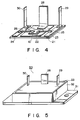
- Fig. 4 is a perspective view showing the arrangement of the assembly of a semiconductor chip and metal connector shown in Fig. 2;
- Fig. 5 is a perspective view of a semiconductor device obtained by sealing the assembly of Fig. 4 in a package; and
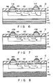
- Figs. 6 to 8 are cross sectional views of chips of metal bump type semiconductor devices according to second to fourth embodiments of this invention.
- Fig. 2 is a cross sectional view of
chip 10 of a solder bump type power bipolar transistor according to a first embodiment of this invention. First,base region 12 andemitter region 13 are formed by a well known method in the main surface area ofsilicon substrate 11 to be used as a collector region. In this embodiment, a high power transistor whose chip size is as large as 10 mm × 10 mm is used as an example, andemitter region 13 is formed with a plurality of divided sections so as to make current flowing in the chip of large area constant.Thermal oxide film 14 is formed on the entire surface ofsubstrate 11 and holes for electrode lead-out ofbase region 12 andemitter region 13 are formed in those portions ofthermal oxide film 14 which lie onbase region 12 andemitter region 13 by a photo-etching process. Next, a layer containing aluminum as the main component (which means an Aℓ layer or Aℓ alloy layer formed by adding Si or Cu of less than several % into Aℓ, for example, and is hereinafter referred to as an Aℓ layer) is formed onthermal oxide film 14 by vapor deposition and then the Aℓ layer is patterned to form baseelectrode wiring pattern 15B and emitterelectrode wiring pattern 15E. After this, insulation film (SiN film) 17 is formed on the entire surface of the resultant semiconductor structure and as a result Aℓ electrode wiring patterns (referred to as Aℓ electrodes) 15B and 15E andthermal oxide film 14 are covered withinsulation film 17. Then, portion ofinsulation film 17 corresponding to Aℓ electrode lead-out areas is selectively removed by photo-etching to expose parts ofAℓ electrodes Ni layer 16 used for the collector electrode lead-out is formed in ohmic contact with and on the other surface (rear surface in Fig. 2) ofsilicon substrate 11. - Solder bumps 18B and 18E are formed directly on the exposed portions of
Aℓ electrodes silicon wafer 61 formed by the above manufacturing method by using an ultrasonic solder bump forming device shown in Fig. 3.Molten solder 53 is received insolder bath 51 of the ultrasonic solder bump forming device.Solder bath 51 is provided withreflux path 52 andmolten solder 53 is moved throughreflux path 52 and raised higher than the liquid level byagitator 54 driven bymotor 56 and is then returned to the main portion.Silicon wafer 61 is supported by a holding member (not shown) and dipped into the pushed-up portion ofmolten solder 53. Further,ultrasonic transducer 55 is inserted into the pushed-up portion ofmolten solder 53 nearsilicon wafer 61 to apply ultrasonic waves tomolten solder 53. - In this embodiment,
molten solder 53 containing Zn of 5 %, Sn of 5 % and Pb of 90 % in mass percentage (hereinafter the composition percentage is simply expressed in % but it should be understood that it expresses the mass percentage) is used. When solder bumps 18B and 18E are formed, ultrasonic waves of frequency of 20 KHz and output power of 80 W were applied byultrasonic transducer 55 andsilicon wafer 61 was kept dipped inmolten solder 53 for 1 second. In the solder bump forming operation, nitrogen gas was supplied around the solder bump forming device at a flow rate of 10 litter/minute to prevent oxidation of Aℓ which is the constituent element ofAℓ electrodes solder bath 51. If the oxide is attached to the surface of solder bumps 18B and 18E whensilicon wafer 61 is pulled out ofsolder bath 51, the attached oxide may become an obstacle to the soldering process effected in the later stage. - After the ultrasonic soldering process is effected, solder bumps 18B and 18E of the height of approx. 80 µm are formed on
Aℓ electrodes solder layer 18C is formed onNi layer 16 on the opposite side ofsubstrate 11. In a case where it is preferable not to formsolder layer 18C onNi layer 16, a mask of polyimide or the like may be previously formed onNi layer 16 before the silicon wafer is dipped intosolder bath 51. - Semiconductor (solder bump type power bipolar transistor) chip as shown in Fig. 2 can be obtained by dicing
silicon wafer 61 havingsolder bumps solder layer 18C is formed onNi layer 16 on the opposite side ofsubstrate 11, it is preferable to effect the blade dicing process after it is attached to an adhesive tape since the surface ofsolder layer 18C is rough. - Next, a process of assembling
semiconductor chip 10 and an electrode lead-out metal member onceramic substrate 21 is explained with reference to Fig. 4. As shown in Fig. 4, a unit having three metal (Cu)plates ceramic substrate 21 is prepared. Then,Ni layer 16 on the collector side ofsemiconductor chip 10 is soldered tometal plate 22 by use ofsolder layer 18C or additional solder. Next,solder bump 18E and solder bump on the emitter side and base side ofsemiconductor chip 10 are soldered tometal plates connectors lead metal plates metal plates ceramic substrate 21 is soldered to heat radiation metal plate 31 (Fig. 5). A sequence of soldering operations described above may be simultaneously effected in a reflow furnace (heat treatment furnace). After this, as shown in Fig. 5,resin casing 32 is mounted,resin 33 is filled inresin casing 32 with the other ends of outerlead metal plates type semiconductor device 50 as shown in Fig. 5 can be obtained. - In
semiconductor device 50 of this invention, ultrasonic waves are applied to the molten solder to form the solder bump directly on the Aℓ electrode. The manufacturing process can be simplified in comparison with the conventional method wherein a solder bump is formed via a backing metal plate. Further, a problem of the conventional manufacturing method that an Aℓ-Sn layer is formed and an eutectic battery is resultantly formed when forming a solder bump directly on the Aℓ electrode by applying ultrasonic waves to Sn-series molten solder can be solved by adding Zn of 5 % in mass percentage into the solder bump. Also, a problem that the Aℓ-Sn alloy layer grows to degrade the bonding property and the absorption action of Aℓ further proceeds because of the heat treatment effected for melting the solder bump for connection with a metal connector after the solder bump has been formed can be markedly suppressed by adding Zn into the solder bump. This may be because an Aℓ-Zn alloy layer is formed on the interface between the Aℓ electrode and the solder bump and functions to suppress the interaction between the Aℓ electrode and the molten solder. Further, in this invention in which the Aℓ-Zn alloy layer is formed, the junction area can be made sufficiently strong in comparison with the case wherein an Sn-series solder containing Ag is used in order to prevent formation of the Aℓ-Sn alloy layer and in this case a weak Aℓ-Ag alloy layer is formed on the interface. As a result, a semiconductor device with high reliability and high productivity can be obtained. - The semiconductor device of the above embodiment is a so-called high power transistor module which is generally used as a switching element for current of several tens of amperes. Conventionally, this type of high power transistor has a number of Aℓ metal fine wires (≦ 500 µmφ) bonded between the emitter Aℓ electrode and the electrode lead-out metal plate by the ultrasonic wire bonding method and has a current capacity of several tens of amperes. However, when an accident happens, a large current of several hundreds of amperes may flow, thereby destroying the ultrasonic bonding portion between the Aℓ fine wires and the Aℓ electrode of the semiconductor chip to separate them from each other. In general, the above transistor is used in a common-emitter connection with several hundreds of volts applied between the emitter and the collector. Therefore, if the Aℓ fine wire of the emitter is peeled or separated from the bonding portion, an arc occurs therebetween to fuse the Aℓ fine wire. Further, another arc may occur between the fused Aℓ metal fine wire and the Aℓ electrode of the chip to extremely raise the temperature in the casing, leading to an accident of blowing up the casing.
- A problem of the high power transistor module manufactured by the conventional metal fine wire bonding method can be solved in the high power transistor module according to one embodiment of this invention. That is, the bonding portion between the metal connector and the Aℓ electrode of the semiconductor chip can be mechanically strengthened by bonding the metal connector and the Aℓ electrode of the semiconductor chip to each other by means of a solder bump (electrode-formation by solder). Therefore, a large current flowing in the above accident will not cause the metal connector to be separated from the bonding portion, preventing the occurrence of an arc. The Aℓ electrode may generally provide a good ohmic contact property when connected with a silicon substrate and can be precisely etched so as to be easily formed in a fine electrode wiring pattern. In the semiconductor device of this invention, highly reliable electrode-formation by solder can be easily attained by forming the Aℓ electrode having the above-described excellent properties by use of the conventional semiconductor chip manufacturing process as it is without effecting complicated succeeding steps of forming a backing metal layer by plating or vapor depositing and difficult selective etching.
- Now, the composition of solder which is important in this invention is explained.
- In the above embodiment, a solder of the composition containing Zn of 5 %, Sn of 5 % and Pb of 90 % is used, but the composition is not limited to this. According to the experiments made by the inventors of this invention, it is confirmed that a solder bump can be formed on the Aℓ electrode if the composition of the solder bump contains Sn of 5 to 95 %, Zn of 1 to 10 % and Pb (the entire remaining portion) and the bonding strength of the junction between the Aℓ electrode and the solder bump can be kept sufficiently high even after the solder bump is melted again. The above confirmation was obtained by effecting a tension test in a direction perpendicular to the junction plane between the Aℓ electrode and the solder bump after the solder bump was melted again and the metal connector was connected thereto. In this case, the "sufficiently high bonding strength" means that a shell crack has occurred in the substrate surface of the chip without causing the peeling in the interface of the alloy layers of the solder or the shear in the solder.
- Further, according to the experiments made by the inventors of this invention, it is confirmed that the bonding strength of the junction between
Aℓ electrodes - Next, the second embodiment of this invention is explained with reference to Fig. 6. Portions in Fig. 6 which correspond to those of Fig. 2 are denoted by the same reference numerals and the explanation therefor is omitted. As shown in Fig. 6, a solder bump is formed with a laminated structure of first and second solder bumps. In this embodiment, the same manufacturing process as in the first embodiment is effected until
Aℓ electrodes Aℓ electrodes solder layer 41C is formed on the rear surface ofchip 10 on the collector electrode side. In this embodiment, first solder bumps 18B and 18E are formed to be 30 µm high on the exposed surfaces ofAℓ electrodes - With this construction, since second solder bumps 41B and 41E can be formed at temperatures lower than the melting point of first solder bumps 18B and 18E, first solder bumps 18B and 18E can be kept in the solid phase during the formation of second solder bumps 41B and 41E and prevented from being melted again. Therefore, the absorption action of Aℓ into first solder bumps 18B and 18E will not proceed. As a result, second solder bumps 41B and 41E can be formed to be as high (thick) as 150 µm, simplifying the step of mounting the metal connector.
- The succeeding manufacturing steps are effected in the same manner as in the first embodiment. Also, the metal connector is connected to second solder bumps 41B and 41E at temperatures lower than the melting point of first solder bumps 18B and 18E. Therefore in the step of mounting the metal connector, first solder bumps 18B and 18E can be kept in the solid phase and prevented from being melted again. As a result, the absorption action of
Aℓ electrodes - Next, the third embodiment of this invention is explained. In this embodiment, a Pb-Sn solder containing Ag (or Cu) is used to form second solder bumps 41B and 41E used in the second embodiment.
- As described in the first embodiment, in a case where
semiconductor chip 10 has an area as large as 10 mm × 10 mm, a stress caused by the difference in thermal expansion betweencollector Ni layer 16 on the rear surface of the chip and metal plate 22 (Fig. 4) for supporting the chip with the solder held therebetween is applied to the solder. The stress may be repeatedly applied to the solder to make it fragile. For this reason, when a chip with a large area is soldered on and supported by a metal plate, much care should be taken to the composition of the solder. In general, it is known in the art that the withstanding ability for the weakening of the solder can be enhanced by using a Pb-Sn solder containing Ag or Cu. - The third embodiment is made with care taken to the improvement of the withstanding ability. That is, in forming first solder bumps 18B and 18E in the second embodiment,
Ni layer 16 to be used as a collector electrode is coated with resin such as polyimide to prevent solder from being attached to first solder bumps 18B and 18E in the step of forming first solder bumps 18B and 18E. Then, after the mask resin is removed, second solder bumps 41B and 41E are formed and at the sametime solder layer 43C having the same solder composition as that of second solder bumps 41B and 41E and containing Ag of 1.5 %, Sn of 5 % and Pb of 93.5 % is formed onNi layer 16 on the collector electrode side. - Next, the fourth embodiment in which the solder composition of first solder bumps 18B and 18E is Aℓ-Zn is explained with reference to Fig. 8.
- In the fourth embodiment, a solder containing Zn of 1 to 10 % and Aℓ as the entire remaining portion (99 to 90 %) is used to form first solder bumps 18B and 18E. Since the melting point of the solder is 380 °C which is slightly higher than others, first solder bumps 18B and 18E can be formed directly on
Aℓ electrodes solder bath 51 is set at 400 °C. According to the experiments, it was found that the height of the solder bump which could be uniformly controlled was approx. 10 µm. In this case, in order to prevent an Aℓ-Zn solder from being attached to the collector electrode, first solder bumps 18B and 18E were formed beforeNi layer 16 was formed, that is, when the silicon surface was still exposed. After this,Ni layer 16 is formed on the rear surface of the chip on the collector electrode side by sputtering and then second solder bumps 41B and 41E are formed. In this case, a solder of the composition containing Ag of 1.5 %, Sn of 5 % and Pb as the entire remaining portion is used to form second solder bumps 41B and 41E. As a result, solder bumps of laminated solder layers of the respective solder composition containing Aℓ-Zn and Pb-Sn-Ag are formed on base andemitter Aℓ electrodes Ag solder layer 45C is formed oncollector Ni layer 16. The succeeding steps are effected in the same manner as in the first embodiment to form the semiconductor device. - In the solder bump type semiconductor device according to the above embodiments of this invention, the composition of the first solder bump contains Zn so that the bonding portion between the Aℓ electrode and the first solder bump can be formed with high reliability. It was confirmed by the experiments made by the inventors of this invention that the bonding strength of the junction between the Aℓ electrode and the bump could be sufficiently high even after it was left for 1000 hours at a temperature of 125 °C.
- In the first to fourth embodiments, the semiconductor device is formed as the power bipolar transistor, but is not limited to it. That is, the Aℓ electrode on the main surface of the semiconductor substrate is formed by a well known method, and the semiconductor device can be a diode, thyristor, GTO, IC or the like if it has the Aℓ electrode thus formed. Further, it is also possible to form a Ti film under the Aℓ electrode, or add Si or Cu into the Aℓ electrode.
- In the above embodiments, the solder composition of the first solder bump contains Zn-Sn-Pb and Zn-Aℓ. However, this invention can be applied to a case wherein the solder composition of the first solder bump contains Zn and an element selected from a group consisting of Sn, Pb and Aℓ, for example, Zn-Sn.
- Reference signs in the claims are intended for better understanding and shall not limit the scope.
Claims (13)
Applications Claiming Priority (2)
| Application Number | Priority Date | Filing Date | Title |
|---|---|---|---|
| JP219726/88 | 1988-09-02 | ||
| JP63219726A JPH0267731A (en) | 1988-09-02 | 1988-09-02 | Solder bump type semiconductor device and manufacture thereof |
Publications (3)
| Publication Number | Publication Date |
|---|---|
| EP0357064A2 true EP0357064A2 (en) | 1990-03-07 |
| EP0357064A3 EP0357064A3 (en) | 1990-09-26 |
| EP0357064B1 EP0357064B1 (en) | 1993-03-10 |
Family
ID=16740009
Family Applications (1)
| Application Number | Title | Priority Date | Filing Date |
|---|---|---|---|
| EP19890116100 Expired - Lifetime EP0357064B1 (en) | 1988-09-02 | 1989-08-31 | Metal bump type semiconductor device and method for manufacturing the same |
Country Status (5)
| Country | Link |
|---|---|
| US (1) | US5143865A (en) |
| EP (1) | EP0357064B1 (en) |
| JP (1) | JPH0267731A (en) |
| KR (1) | KR0143086B1 (en) |
| DE (1) | DE68905267T2 (en) |
Cited By (4)
| Publication number | Priority date | Publication date | Assignee | Title |
|---|---|---|---|---|
| DE4316175A1 (en) * | 1993-05-14 | 1994-11-17 | Daimler Benz Ag | Soldered connection and soldering method |
| EP0763853A1 (en) * | 1995-09-18 | 1997-03-19 | Texas Instruments Incorporated | Improvements in or relating to integrated circuits |
| WO1998040912A1 (en) * | 1997-03-10 | 1998-09-17 | Fraunhofer-Gesellschaft zur Förderung der angewandten Forschung e.V. | Chip arrangement and method for the production of the same |
| EP0899786A2 (en) * | 1997-08-25 | 1999-03-03 | Showa Denko K K | Silicon semiconductor device with an electrode structure and circuit board having the device mounted thereon |
Families Citing this family (36)
| Publication number | Priority date | Publication date | Assignee | Title |
|---|---|---|---|---|
| US5360988A (en) * | 1991-06-27 | 1994-11-01 | Hitachi, Ltd. | Semiconductor integrated circuit device and methods for production thereof |
| US5444300A (en) * | 1991-08-09 | 1995-08-22 | Sharp Kabushiki Kaisha | Semiconductor apparatus with heat sink |
| US5824569A (en) * | 1992-07-15 | 1998-10-20 | Micron Technology, Inc. | Semiconductor device having ball-bonded pads |
| US5496775A (en) * | 1992-07-15 | 1996-03-05 | Micron Semiconductor, Inc. | Semiconductor device having ball-bonded pads |
| US5766972A (en) * | 1994-06-02 | 1998-06-16 | Mitsubishi Denki Kabushiki Kaisha | Method of making resin encapsulated semiconductor device with bump electrodes |
| JP3348528B2 (en) * | 1994-07-20 | 2002-11-20 | 富士通株式会社 | Method for manufacturing semiconductor device, method for manufacturing semiconductor device and electronic circuit device, and electronic circuit device |
| JPH08191104A (en) | 1995-01-11 | 1996-07-23 | Hitachi Ltd | Semiconductor integrated circuit device and manufacturing method thereof |
| US5668058A (en) * | 1995-12-28 | 1997-09-16 | Nec Corporation | Method of producing a flip chip |
| KR100186333B1 (en) * | 1996-06-20 | 1999-03-20 | 문정환 | Chip-sized semiconductor package and its manufacturing method |
| US6881611B1 (en) | 1996-07-12 | 2005-04-19 | Fujitsu Limited | Method and mold for manufacturing semiconductor device, semiconductor device and method for mounting the device |
| CN1110846C (en) * | 1996-07-12 | 2003-06-04 | 富士通株式会社 | Method and mold for manufacturing semiconductor device, semiconductor device, and method for mounting the device |
| JP3409598B2 (en) * | 1996-08-29 | 2003-05-26 | ソニー株式会社 | Method for manufacturing semiconductor device |
| US6127735A (en) * | 1996-09-25 | 2000-10-03 | International Business Machines Corporation | Interconnect for low temperature chip attachment |
| JP3796016B2 (en) * | 1997-03-28 | 2006-07-12 | 三洋電機株式会社 | Semiconductor device |
| US6082610A (en) | 1997-06-23 | 2000-07-04 | Ford Motor Company | Method of forming interconnections on electronic modules |
| US20070102827A1 (en) * | 1997-12-08 | 2007-05-10 | 3M Innovative Properties Company | Solvent Assisted Burnishing of Pre-Underfilled Solder-Bumped Wafers for Flipchip Bonding |
| US6260264B1 (en) * | 1997-12-08 | 2001-07-17 | 3M Innovative Properties Company | Methods for making z-axis electrical connections |
| US6423623B1 (en) * | 1998-06-09 | 2002-07-23 | Fairchild Semiconductor Corporation | Low Resistance package for semiconductor devices |
| US6251765B1 (en) * | 1998-07-10 | 2001-06-26 | Ball Semiconductor, Inc. | Manufacturing metal dip solder bumps for semiconductor devices |
| JP3420703B2 (en) * | 1998-07-16 | 2003-06-30 | 株式会社東芝 | Method for manufacturing semiconductor device |
| JP2000216184A (en) * | 1999-01-25 | 2000-08-04 | Sanyo Electric Co Ltd | Semiconductor device and manufacture thereof |
| US6717245B1 (en) * | 2000-06-02 | 2004-04-06 | Micron Technology, Inc. | Chip scale packages performed by wafer level processing |
| US7214566B1 (en) * | 2000-06-16 | 2007-05-08 | Micron Technology, Inc. | Semiconductor device package and method |
| US20020071293A1 (en) * | 2000-07-13 | 2002-06-13 | Eden Richard C. | Power semiconductor switching devices, power converters, integrated circuit assemblies, integrated circuitry, power current switching methods, methods of forming a power semiconductor switching device, power conversion methods, power semiconductor switching device packaging methods, and methods a of forming power transistor |
| US6902098B2 (en) * | 2001-04-23 | 2005-06-07 | Shipley Company, L.L.C. | Solder pads and method of making a solder pad |
| JP4143478B2 (en) * | 2002-10-02 | 2008-09-03 | アルプス電気株式会社 | Solder connection structure and solder connection method for electronic parts |
| US7868472B2 (en) * | 2004-04-08 | 2011-01-11 | Avago Technologies General Ip (Singapore) Pte. Ltd. | Thermal dissipation in integrated circuit systems |
| US7109583B2 (en) * | 2004-05-06 | 2006-09-19 | Endwave Corporation | Mounting with auxiliary bumps |
| US20060038302A1 (en) * | 2004-08-19 | 2006-02-23 | Kejun Zeng | Thermal fatigue resistant tin-lead-silver solder |
| US7768075B2 (en) | 2006-04-06 | 2010-08-03 | Fairchild Semiconductor Corporation | Semiconductor die packages using thin dies and metal substrates |
| JP4708399B2 (en) * | 2007-06-21 | 2011-06-22 | 新光電気工業株式会社 | Electronic device manufacturing method and electronic device |
| WO2009083849A2 (en) * | 2007-12-20 | 2009-07-09 | Koninklijke Philips Electronics, N.V. | Direct conversion detector |
| US8169081B1 (en) | 2007-12-27 | 2012-05-01 | Volterra Semiconductor Corporation | Conductive routings in integrated circuits using under bump metallization |
| US20090194856A1 (en) * | 2008-02-06 | 2009-08-06 | Gomez Jocel P | Molded package assembly |
| KR101055485B1 (en) * | 2008-10-02 | 2011-08-08 | 삼성전기주식회사 | Semiconductor package with bumpball |
| US20150001706A1 (en) * | 2013-06-27 | 2015-01-01 | Kabirkumar Mirpuri | Systems and methods for avoiding protrusions in injection molded solder |
Citations (1)
| Publication number | Priority date | Publication date | Assignee | Title |
|---|---|---|---|---|
| EP0264648A1 (en) * | 1986-09-25 | 1988-04-27 | Kabushiki Kaisha Toshiba | Method of producing a film carrier |
Family Cites Families (19)
| Publication number | Priority date | Publication date | Assignee | Title |
|---|---|---|---|---|
| JPS5344176A (en) * | 1976-10-04 | 1978-04-20 | Hitachi Cable Ltd | Clad solder for semiconductor device |
| JPS5389368A (en) * | 1977-01-17 | 1978-08-05 | Seiko Epson Corp | Production of semiconductor integrated circuit |
| JPS5426675A (en) * | 1977-07-29 | 1979-02-28 | Matsushita Electric Ind Co Ltd | Manufacture for semiconductor device |
| NL7810942A (en) * | 1978-11-03 | 1980-05-07 | Philips Nv | SUPPORTED MICROSTRIP LINE FOR PROPAGING AN ODD WAVE MODE. |
| JPS55163830A (en) * | 1979-06-07 | 1980-12-20 | Marukon Denshi Kk | Condenser |
| JPS592142B2 (en) * | 1980-01-18 | 1984-01-17 | 松下電子工業株式会社 | direct view storage tube |
| US4351180A (en) * | 1980-06-30 | 1982-09-28 | The National Machinery Company | Workpiece turning transfer |
| JPS5778173A (en) * | 1980-11-04 | 1982-05-15 | Hitachi Ltd | Semiconductor device and manufacture thereof |
| JPS5851511A (en) * | 1981-09-22 | 1983-03-26 | Mitsubishi Electric Corp | Forming method for electrode of semiconductor device |
| JPS5942197A (en) * | 1982-08-31 | 1984-03-08 | Matsushita Electric Works Ltd | Solder |
| JPS5977244U (en) * | 1982-11-15 | 1984-05-25 | 日本電気株式会社 | semiconductor equipment |
| JPS5990941A (en) * | 1982-11-17 | 1984-05-25 | Nec Home Electronics Ltd | Bump plating method |
| JPS59178778A (en) * | 1983-03-30 | 1984-10-11 | Toshiba Corp | Solar battery and manufacture thereof |
| JPS59181627A (en) * | 1983-03-31 | 1984-10-16 | Toshiba Corp | Manufacture of semiconductor device |
| JPS592142U (en) * | 1983-04-20 | 1984-01-09 | セイコーエプソン株式会社 | semiconductor integrated circuit |
| JPS6159548A (en) * | 1984-08-30 | 1986-03-27 | Fujitsu Ltd | Logic simulation processor |
| JPS62104143A (en) * | 1985-10-31 | 1987-05-14 | Toshiba Corp | Formation of solder bump |
| IT1191977B (en) * | 1986-06-30 | 1988-03-31 | Selenia Ind Elettroniche | TECHNIQUE TO ALIGN WITH CONVENTIONAL PHOTOLITHOGRAPHY A STRUCTURE ON THE BACK OF A SAMPLE WITH HIGH RECORDING PRECISION |
| JPH01220460A (en) * | 1988-02-29 | 1989-09-04 | Omron Tateisi Electron Co | Bump forming solder for semiconductor device |
-
1988
- 1988-09-02 JP JP63219726A patent/JPH0267731A/en active Granted
-
1989
- 1989-08-31 EP EP19890116100 patent/EP0357064B1/en not_active Expired - Lifetime
- 1989-08-31 DE DE1989605267 patent/DE68905267T2/en not_active Expired - Fee Related
- 1989-09-02 KR KR1019890012709A patent/KR0143086B1/en not_active IP Right Cessation
-
1991
- 1991-07-17 US US07/731,392 patent/US5143865A/en not_active Expired - Lifetime
Patent Citations (1)
| Publication number | Priority date | Publication date | Assignee | Title |
|---|---|---|---|---|
| EP0264648A1 (en) * | 1986-09-25 | 1988-04-27 | Kabushiki Kaisha Toshiba | Method of producing a film carrier |
Non-Patent Citations (1)
| Title |
|---|
| ELECTRONICS AND COMMUNICATIONS IN JAPAN, part 2, vol. 71, no. 10, 1988, pages 32-38, originally published on November 1987 in Denshi Joho Tsushin Gakkai Ronbunshi, vol. 70-C, no. 11, pages 1466-1472, Scripta Technica, Inc.; M. INABA et al.: "Direct formation of solder bump on Al pad using ultrasonic soldering" * |
Cited By (6)
| Publication number | Priority date | Publication date | Assignee | Title |
|---|---|---|---|---|
| DE4316175A1 (en) * | 1993-05-14 | 1994-11-17 | Daimler Benz Ag | Soldered connection and soldering method |
| EP0763853A1 (en) * | 1995-09-18 | 1997-03-19 | Texas Instruments Incorporated | Improvements in or relating to integrated circuits |
| WO1998040912A1 (en) * | 1997-03-10 | 1998-09-17 | Fraunhofer-Gesellschaft zur Förderung der angewandten Forschung e.V. | Chip arrangement and method for the production of the same |
| EP0899786A2 (en) * | 1997-08-25 | 1999-03-03 | Showa Denko K K | Silicon semiconductor device with an electrode structure and circuit board having the device mounted thereon |
| EP0899786A3 (en) * | 1997-08-25 | 2000-01-19 | Showa Denko K K | Silicon semiconductor device with an electrode structure and circuit board having the device mounted thereon |
| US6221692B1 (en) | 1997-08-25 | 2001-04-24 | Showa Denko, K.K. | Method of fabricating solder-bearing silicon semiconductor device and circuit board mounted therewith |
Also Published As
| Publication number | Publication date |
|---|---|
| DE68905267D1 (en) | 1993-04-15 |
| US5143865A (en) | 1992-09-01 |
| JPH0267731A (en) | 1990-03-07 |
| DE68905267T2 (en) | 1993-09-09 |
| EP0357064B1 (en) | 1993-03-10 |
| JPH054809B2 (en) | 1993-01-20 |
| EP0357064A3 (en) | 1990-09-26 |
| KR900005585A (en) | 1990-04-14 |
| KR0143086B1 (en) | 1998-07-01 |
Similar Documents
| Publication | Publication Date | Title |
|---|---|---|
| EP0357064A2 (en) | Metal bump type semiconductor device and method for manufacturing the same | |
| US8022551B2 (en) | Solder composition for electronic devices | |
| EP0435009A2 (en) | Semiconductor package connecting method, semiconductor package connecting wires and semiconductor devices | |
| US6440835B1 (en) | Method of connecting a conductive trace to a semiconductor chip | |
| US6378758B1 (en) | Conductive leads with non-wettable surfaces | |
| US20040150083A1 (en) | Method for manufacturing digital micro-mirror device (DMD) | |
| JP2003264366A (en) | Electronic apparatus | |
| US6350632B1 (en) | Semiconductor chip assembly with ball bond connection joint | |
| JPH0378230A (en) | Bump electrode for integrated circuit device | |
| JP3868766B2 (en) | Semiconductor device | |
| JP3356649B2 (en) | Semiconductor device and manufacturing method thereof | |
| US6511865B1 (en) | Method for forming a ball bond connection joint on a conductive trace and conductive pad in a semiconductor chip assembly | |
| JPS62281435A (en) | Semiconductor device | |
| JPS60134444A (en) | Formation for bump electrode | |
| JP3210456B2 (en) | Method of forming ball on metal wire | |
| JP3006957B2 (en) | Semiconductor device package | |
| JPS6143438A (en) | Semiconductor device | |
| JP3454097B2 (en) | Electronic component and method of manufacturing electronic component | |
| JP2911005B2 (en) | Processing method of bump electrode | |
| JPH0732170B2 (en) | Semiconductor device | |
| JPS62104143A (en) | Formation of solder bump | |
| JPH0727905B2 (en) | Method of forming solder bumps | |
| JPS63142643A (en) | Semiconductor device | |
| JPH0727904B2 (en) | Method of forming solder bumps | |
| JPS63318744A (en) | Semiconductor device |
Legal Events
| Date | Code | Title | Description |
|---|---|---|---|
| PUAI | Public reference made under article 153(3) epc to a published international application that has entered the european phase |
Free format text: ORIGINAL CODE: 0009012 |
|
| 17P | Request for examination filed |
Effective date: 19890831 |
|
| AK | Designated contracting states |
Kind code of ref document: A2 Designated state(s): DE FR GB |
|
| PUAL | Search report despatched |
Free format text: ORIGINAL CODE: 0009013 |
|
| AK | Designated contracting states |
Kind code of ref document: A3 Designated state(s): DE FR GB |
|
| 17Q | First examination report despatched |
Effective date: 19920429 |
|
| GRAA | (expected) grant |
Free format text: ORIGINAL CODE: 0009210 |
|
| AK | Designated contracting states |
Kind code of ref document: B1 Designated state(s): DE FR GB |
|
| REF | Corresponds to: |
Ref document number: 68905267 Country of ref document: DE Date of ref document: 19930415 |
|
| ET | Fr: translation filed | ||
| PLBE | No opposition filed within time limit |
Free format text: ORIGINAL CODE: 0009261 |
|
| STAA | Information on the status of an ep patent application or granted ep patent |
Free format text: STATUS: NO OPPOSITION FILED WITHIN TIME LIMIT |
|
| 26N | No opposition filed | ||
| REG | Reference to a national code |
Ref country code: GB Ref legal event code: 746 Effective date: 19981023 |
|
| REG | Reference to a national code |
Ref country code: FR Ref legal event code: D6 |
|
| REG | Reference to a national code |
Ref country code: GB Ref legal event code: IF02 |
|
| PGFP | Annual fee paid to national office [announced via postgrant information from national office to epo] |
Ref country code: FR Payment date: 20020808 Year of fee payment: 14 |
|
| PGFP | Annual fee paid to national office [announced via postgrant information from national office to epo] |
Ref country code: GB Payment date: 20020828 Year of fee payment: 14 |
|
| PGFP | Annual fee paid to national office [announced via postgrant information from national office to epo] |
Ref country code: DE Payment date: 20020904 Year of fee payment: 14 |
|
| PG25 | Lapsed in a contracting state [announced via postgrant information from national office to epo] |
Ref country code: GB Free format text: LAPSE BECAUSE OF NON-PAYMENT OF DUE FEES Effective date: 20030831 |
|
| PG25 | Lapsed in a contracting state [announced via postgrant information from national office to epo] |
Ref country code: DE Free format text: LAPSE BECAUSE OF NON-PAYMENT OF DUE FEES Effective date: 20040302 |
|
| GBPC | Gb: european patent ceased through non-payment of renewal fee | ||
| PG25 | Lapsed in a contracting state [announced via postgrant information from national office to epo] |
Ref country code: FR Free format text: LAPSE BECAUSE OF NON-PAYMENT OF DUE FEES Effective date: 20040430 |
|
| REG | Reference to a national code |
Ref country code: FR Ref legal event code: ST |