EP0357410A2 - Semiconductor integrated circuit device - Google Patents
Semiconductor integrated circuit device Download PDFInfo
- Publication number
- EP0357410A2 EP0357410A2 EP89308798A EP89308798A EP0357410A2 EP 0357410 A2 EP0357410 A2 EP 0357410A2 EP 89308798 A EP89308798 A EP 89308798A EP 89308798 A EP89308798 A EP 89308798A EP 0357410 A2 EP0357410 A2 EP 0357410A2
- Authority
- EP
- European Patent Office
- Prior art keywords
- circuit device
- transistors
- conduction type
- integrated circuit
- source
- Prior art date
- Legal status (The legal status is an assumption and is not a legal conclusion. Google has not performed a legal analysis and makes no representation as to the accuracy of the status listed.)
- Granted
Links
Images


Classifications
-
- G—PHYSICS
- G11—INFORMATION STORAGE
- G11C—STATIC STORES
- G11C11/00—Digital stores characterised by the use of particular electric or magnetic storage elements; Storage elements therefor
- G11C11/21—Digital stores characterised by the use of particular electric or magnetic storage elements; Storage elements therefor using electric elements
- G11C11/34—Digital stores characterised by the use of particular electric or magnetic storage elements; Storage elements therefor using electric elements using semiconductor devices
-
- H—ELECTRICITY
- H01—ELECTRIC ELEMENTS
- H01L—SEMICONDUCTOR DEVICES NOT COVERED BY CLASS H10
- H01L27/00—Devices consisting of a plurality of semiconductor or other solid-state components formed in or on a common substrate
- H01L27/02—Devices consisting of a plurality of semiconductor or other solid-state components formed in or on a common substrate including semiconductor components specially adapted for rectifying, oscillating, amplifying or switching and having at least one potential-jump barrier or surface barrier; including integrated passive circuit elements with at least one potential-jump barrier or surface barrier
- H01L27/04—Devices consisting of a plurality of semiconductor or other solid-state components formed in or on a common substrate including semiconductor components specially adapted for rectifying, oscillating, amplifying or switching and having at least one potential-jump barrier or surface barrier; including integrated passive circuit elements with at least one potential-jump barrier or surface barrier the substrate being a semiconductor body
- H01L27/08—Devices consisting of a plurality of semiconductor or other solid-state components formed in or on a common substrate including semiconductor components specially adapted for rectifying, oscillating, amplifying or switching and having at least one potential-jump barrier or surface barrier; including integrated passive circuit elements with at least one potential-jump barrier or surface barrier the substrate being a semiconductor body including only semiconductor components of a single kind
- H01L27/085—Devices consisting of a plurality of semiconductor or other solid-state components formed in or on a common substrate including semiconductor components specially adapted for rectifying, oscillating, amplifying or switching and having at least one potential-jump barrier or surface barrier; including integrated passive circuit elements with at least one potential-jump barrier or surface barrier the substrate being a semiconductor body including only semiconductor components of a single kind including field-effect components only
- H01L27/088—Devices consisting of a plurality of semiconductor or other solid-state components formed in or on a common substrate including semiconductor components specially adapted for rectifying, oscillating, amplifying or switching and having at least one potential-jump barrier or surface barrier; including integrated passive circuit elements with at least one potential-jump barrier or surface barrier the substrate being a semiconductor body including only semiconductor components of a single kind including field-effect components only the components being field-effect transistors with insulated gate
- H01L27/092—Devices consisting of a plurality of semiconductor or other solid-state components formed in or on a common substrate including semiconductor components specially adapted for rectifying, oscillating, amplifying or switching and having at least one potential-jump barrier or surface barrier; including integrated passive circuit elements with at least one potential-jump barrier or surface barrier the substrate being a semiconductor body including only semiconductor components of a single kind including field-effect components only the components being field-effect transistors with insulated gate complementary MIS field-effect transistors
- H01L27/0925—Devices consisting of a plurality of semiconductor or other solid-state components formed in or on a common substrate including semiconductor components specially adapted for rectifying, oscillating, amplifying or switching and having at least one potential-jump barrier or surface barrier; including integrated passive circuit elements with at least one potential-jump barrier or surface barrier the substrate being a semiconductor body including only semiconductor components of a single kind including field-effect components only the components being field-effect transistors with insulated gate complementary MIS field-effect transistors comprising an N-well only in the substrate
-
- H—ELECTRICITY
- H01—ELECTRIC ELEMENTS
- H01L—SEMICONDUCTOR DEVICES NOT COVERED BY CLASS H10
- H01L27/00—Devices consisting of a plurality of semiconductor or other solid-state components formed in or on a common substrate
- H01L27/02—Devices consisting of a plurality of semiconductor or other solid-state components formed in or on a common substrate including semiconductor components specially adapted for rectifying, oscillating, amplifying or switching and having at least one potential-jump barrier or surface barrier; including integrated passive circuit elements with at least one potential-jump barrier or surface barrier
- H01L27/04—Devices consisting of a plurality of semiconductor or other solid-state components formed in or on a common substrate including semiconductor components specially adapted for rectifying, oscillating, amplifying or switching and having at least one potential-jump barrier or surface barrier; including integrated passive circuit elements with at least one potential-jump barrier or surface barrier the substrate being a semiconductor body
-
- H—ELECTRICITY
- H10—SEMICONDUCTOR DEVICES; ELECTRIC SOLID-STATE DEVICES NOT OTHERWISE PROVIDED FOR
- H10B—ELECTRONIC MEMORY DEVICES
- H10B20/00—Read-only memory [ROM] devices
Definitions
- the present invention relates to a semiconductor integrated circuit device, for example to a semiconductor delay circuit device having a plurality of inverter circuits which are cascade-connected.
- a semiconductor delay circuit device is used for an optical disc system, for example, a laser disc system or a compact disc system.
- the semiconductor delay circuit device is used for delaying a detected signal of the optical disc system to maintain synchronization even if the center position of the optical disc is shifted. Namely, since the center position of an optical disc cannot be formed perfectly at the exact center of the disc in a production step, a semiconductor delay circuit device should be provided in the optical disc system for synchronization.
- the semiconductor delay circuit device is, for example, constituted by a plurality of inverter circuits which are cascade-connected, and an input signal of the semiconductor delay circuit device is delayed in accordance with a value of a power supply voltage applied to the plurality of inverter circuits in the semiconductor delay circuit device.
- inverter circuits are arranged adjacent to one another.
- the same conduction type (P-channel type or N-channel type) transistors of the plurality of inverter circuits in the semiconductor delay circuit device are then arranged such that their source regions are integrally formed with each other to constitute a common source region.
- a substrate contact diffusion region which is an N+ layer or P+ layer that is an opposite conduction type relative to the common source region and has a higher impurity density than a substrate, is arranged for the common source region separately from the common source region.
- the common source region and substrate contact diffusion region are connected to power sources through aluminum wirings.
- an operation current of the transistor flows to an aluminum wiring through the common source region, that is, the operation current of the transistor does not flow only through a source region, which is the common source region, of the specific transistor, but also flows through a source region, which is also the common source region, of a transistor neighboring the specific transistor. Then, due to contact resistance between the common source region and the aluminum wiring, etc., source potentials of the specific and neighboring transistors which have the common source region may be influenced by each other.
- An embodiment of the present invention may provide a semiconductor integrated circuit device having an effect where operation current flowing to one transistor never influences a source potential of another transistor adjacent to and facing the first transistor. Further, an embodiment of the present invention may provide a semiconductor integrated circuit device having a miniaturized pattern and a reduced layout area made as small as possible. Additionally, an embodiment of the present invention may provide a semiconductor integrated circuit device having an output waveform duty ratio equal to that of a first input waveform.
- a semiconductor integrated circuit device comprising a pair of transistors of the same conduction type having source regions receiving a common power supply voltage, the source regions being arranged adjacent to each other and facing each other; and a substrate contact diffusion region whose conduction type is opposite to that of the source regions, the substrate contact diffusion region extending between the source regions. Therefore, the source regions do not influence each other.
- the semiconductor integrated circuit device may comprise a plurality of pairs of the same conduction type transistors.
- a substrate contact diffusion region may extend to respective source regions of the pairs of transistors in adjacent stages and protruding to approach channel forming regions of the transistors having the respective source regions.
- an embodiment of the present invention may provide a semiconductor integrated circuit device comprising a first power supply line, a second power supply line, and a plurality of inverter circuits.
- the inverter circuits are cascade-connected and each of the inverter circuits is connected to the first and second power supply lines.
- Each of the inverter circuits is constituted by a first conduction type transistor and a second conduction type transistor.
- a pair of transistors of the same conduction type has source regions that are arranged adjacent to each other and facing each other.
- the conduction type of the substrate contact diffusion region is opposite to that of the source regions and which has higher impurity density than the substrate.
- the substrate contact diffusion region may have a higher impurity density than the substrate.
- the first conduction type transistor may be a P-channel type transistor and the second conduction type transistor may be an N-channel type transistor, and the first power supply line may be used for applying a high potential power supply to a source region of each P-channel type transistor of the inverter circuits and the second power supply line may be used for applying a low potential power supply to a source region of each N-channel type transistor of the inverter circuits.
- the substrate contact diffusion region between the source regions of the pair of transistors may include a contact portion for connecting aluminum wiring.
- the distance of the substrate contact diffusion region between the source regions of the pair of transistors may be less than the minimum width of diffusion.
- the distance of the substrate contact diffusion region between the source regions of the pair of transistors may be less than 4 microns.
- the plurality of inverter circuits may be arranged in plural rows, sequentially turned an even number of times and cascade-connected, the number of stages of the inverter circuits in each row may be odd. the number of stages of the inverter circuits in the last row may be even.
- An ON resistance value of the first conduction type transistor may differ from that of the second conduction type transistor.
- an embodiment of the present invention may provide a semiconductor integrated circuit device comprising a first power supply line, a second power supply line, and a plurality of inverter circuits.
- the inverter circuits are cascade-connected and each of the inverter circuits is connected to the first and second power supply lines, and each of the inverter circuits is constituted by a first conduction type transistor and a second conduction type transistor.
- Source and drain regions of the first and second conduction type transistors are arranged so that extensions of lines connecting the respective source and drain regions of the first and second conduction type transistors intersect each other, and a conductive layer having gate electrodes is disposed orthogonal to the source and drain regions.
- a plan shape of a wiring contact provided for each of the source and drain regions of the first and second conduction type transistors may be hexagonal.
- the wiring for connecting the drain regions of the first and second conduction type transistors with each other may be curved opposite to a curve of the conductive layer having the gate electrodes of the first and second conduction type transactors.
- the wiring for connecting the drain regions of the first and second conduction type transistors with each other may be connected to a conductive layer having respective gate electrodes of an inverter circuit of the next stage.
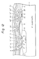
- Figure 1 is a plan view showing a layout of a single inverter portion of a semiconductor delay circuit device in a prior proposal.
- the semiconductor delay circuit device is used for an optical disc system, and is used for delaying a detected signal of the optical disc system to maintain synchronization, even if a center position of the optical disc is shifted. Namely, since the center position of the optical disc cannot be formed perfectly at the exact center of the disc in a production step, a semiconductor delay circuit device should be provided in the optical disc system for synchronization.
- the semiconductor delay circuit device is, for example, constituted by a plurality of inverter circuits which are cascade-connected, and an input signal of the semiconductor delay circuit device is delayed in accordance with a value of a power supply voltage applied to the plurality of inverter circuits in the semiconductor delay circuit device.
- an N-channel transistor Qn′ and a P-channel transistor Qp′ constitute the inverter circuit.
- Figure 2 is a sectional view showing the single inverter portion of the semiconductor delay circuit device shown in Fig. 1.
- the N-channel transistor Qn′ comprises an N+ diffusion layer acting as a source diffusion region 21′ and a drain diffusion region 22′. Adjacent to the source diffusion region 21′, there is a P+ diffusion layer acting as a substrate contact diffusion region 31′.
- the numeral 4′ is a polysilicon layer acting as a common gate electrode with respect to the N-channel transistor Qn′ and P-channel transistor Qp′ (which is not shown in Fig. 2).
- the numeral 41′ is an aluminum wire for input signals connected to the polysilicon layer 4′.
- the numeral 5′ is an aluminum wire connected to the source diffusion region 21′ and substrate contact diffusion region 31′ at respective contact portions 51′ and 52′.
- the aluminum wire 5′ is, for example, connected to a low potential power source Vss.
- the numeral 6′ is an aluminum wire connecting the drain diffusion region 22′ of the N-channel transistor Qn′ to a drain diffusion region (P+ layer) 23′ of the P-channel transistor Qp′ at respective contact portions 61′ and 62′. Through the aluminum wire 6′, output signals of the inverter circuit are picked up.
- FIG. 1 is an equivalent circuit view showing the single inverter portion of the semiconductor delay circuit device shown in Fig. 1.
- Figure 1 shows only the layout of the portion constituting the single inverter in the semiconductor delay circuit device. Recently such a layout pattern of a semiconductor delay circuit device tends to be increasingly miniaturized.
- an inverter for example the one mentioned above, is arranged adjacent to another inverter.
- the same conduction type (P-channel type or N-channel type) transistors are then arranged such that their source regions are integrally formed with each other to constitute a common source region.
- a substrate contact diffusion layer (region) which is an N+ layer or P+ layer that is of an opposite conduction type relative to the common source region and has a higher impurity density than a substrate, is arranged for the common source region, and separately from the common source region.
- the common source region and substrate contact diffusion region are connected to a predetermined power source via aluminum wiring.
- Embodiments of the present invention may solve such a problem. Even if source regions of a pair of the same conduction type transistors are arranged adjacent to each other and facing each other, the source regions are separated by a substrate contact diffusion region that is of an opposite conduction type relative to the source regions and has a higher impurity density than the substrate. As a result, the effect of an operation current flowing to one transistor never influences a source of the other transistor.
- the lines that connect the respective source and drain regions of the P-channel and N-channel transistors run in parallel with each other.
- the polysilicon layer having the gate electrodes of the respective transistors and the aluminum wiring for connecting the drain regions of the respective transistors are constituted by combining linear portions. Accordingly, a pattern forming a single inverter circuit, or in other words, an area needed for the layout of the inverter circuit, may have many useless portions making the overall pattern larger.
- Embodiments of the invention may also solve the above problem, so that the pattern of an inverter circuit can be miniaturized and improved to reduce the layout area to be as small as possible, or to increase the number of inverter circuits to be arranged in a unit area as much as possible.
- Figure 4 is a block view showing an optical disc system for an example of using the semiconductor delay circuit device.
- a semiconductor delay circuit device is used for an optical disc system, and is used for delaying a detected signal of the optical disc system to maintain synchronization, even if a center position of an optical disc is shifted.
- an optical disc system is basically constituted by a pickup 401, a semiconductor delay circuit device (phase controller) 402, an FM-detection portion 403, a synchronizing signal select portion 404, and a phase difference detector 405.
- Data for example, a video signal data or an audio signal data
- An output signal of the semiconductor delay circuit device 402 is supplied to the FM-detection portion 403, and an output signal of the optical disc system, for example, a video signal or an audio signal, is output from the FM-detection portion 403.
- a synchronizing signal is selected by the synchronizing signal select portion 404 via the FM-detection portion 403, and the output signal of the synchronizing signal select portion 404 is supplied to the phase difference detector 405.
- the phase difference detector 405 is also supplied with a reference signal, and the phase difference detector 405 outputs a voltage control signal to the semiconductor delay circuit device 402 by comparing the synchronizing signal from the synchronizing signal select portion 404 and the reference signal.
- the output signal of the pickup 401 is a frequency modulated signal including a phase fluctuation of ⁇ 27 ⁇ sec., and this phase fluctuation is caused by, for example, an eccentricity of a center position in the optical disc 400.
- the center position of the optical disc 400 cannot be formed perfectly at the exact center of the disc in a production step, so the semiconductor delay circuit device 402 is used for delaying the output signal from the pickup 401 to maintain a synchronization in accordance with the voltage control signal output from the phase difference detector 405.
- the semiconductor delay circuit device 402 is, for example, constituted by a plurality of inverter circuits which are cascade-connected, and the output signal of the pickup 401 is delayed for synchronizing by the synchronizing signal from the synchronizing signal select portion 404 and the reference signal in accordance with a value of a power supply voltage, which is the voltage control signal, applied to the plurality of inverter circuits in the semiconductor delay circuit device. Consequently, the output signal of the optical disc system, which is the output signal of the FM-detection portion 403, is maintained in a stable state with no phase fluctuation.
- a delay value of the semiconductor delay circuit device 402 is determined to be a value larger than the phase fluctuation range (for example, ⁇ 27 ⁇ sec.) of the frequency modulated signal picked up by the pickup 401.
- the delay value of the semiconductor delay circuit device 402 is determined to be 60 ⁇ sec.
- Figure 5 is a circuit view showing the semiconductor delay circuit device shown in Fig. 4.
- the semiconductor delay circuit device 402 is constituted by a plurality of inverter circuits I1 , I2 , I3 , ... , I n-1 , I n , I n+1 , ...
- the semiconductor delay circuit device 402 is constituted by a plurality of rows R1 , R2 , R3 , ... with each of the rows including a few hundred inverters, and the semiconductor delay circuit device 402 is constituted by 24000 stages of inverter circuits which are cascade-connected.
- Figures 6 to 8 show a layout of a semiconductor delay circuit device according to an embodiment of the present invention.
- multistage inverter circuits which comprise P-channel transistors and N-channel transistors, are cascade-connected. Namely, wiring (aluminum wiring) for connecting respective drain regions of a predetermined inverter circuit is connected to a conductive layer, for example, a polysilicon layer, having respective gate electrodes of an inverter circuit of the next stage.
- a conductive layer for example, a polysilicon layer
- Figure 6 shows a layout pattern including source and drain diffusion regions of the P-channel transistors and N-channel transistors that constitute inverter circuits, polysilicon layers having gate electrodes of the respective transistors, and substrate (power source) contact diffusion layers (regions) that are arranged between respective source regions of the P-channel transistors constituting adjacent inverters and between respective source regions of the N-channel transistors constituting adjacent inverters.
- numerals 21 and 22 are source and drain regions (both P+ diffusion layers) of the P-channel transistor constituting a predetermined inverter, respectively.
- Numerals 23 and 24 are source and drain regions (both N+ diffusion layers) of the N-channel transistor constituting the inverter, respectively.
- Numeral 51 is a polysilicon layer. Both edge portions 51′ and 52 ⁇ of the polysilicon layer function as gate electrodes of the P-channel transistor and N-channel transistor.
- Numeral 52 is a polysilicon layer having gate electrodes of respective transistors constituting an inverter of the next stage. The polysilicon layer 52 is connected to aluminum wiring which is indicated as a first layer aluminum wiring 62 in Figs.
- Numerals 62′, 62 ⁇ and 62′′′ are aluminum contacts, for example, refer to Fig. 11, for connecting the aluminum wiring 62 to the drain regions 22 and 24 and polysilicon layer 52.
- Numerals 31 and 32 are substrate contact diffusion regions (N+ diffusion layers) arranged between the respective source regions of P-channel transistors that constitute adjacent inverters.
- the substrate contact diffusion region 31 is arranged to interpose between the source regions 21 and 21′ of the P-channel transistors that face each other in the length direction, i.e., the P-channel transistors that constitute inverters of adjacent columns.
- the width of the region 31, i.e., a facing distance of the source regions 21 and 21′, may be narrower than, for example, the minimum channel length of one of the transistors constituting the inverter (in this example, the channel length of the P-channel transistor).
- Numerals 22′ and 53 ⁇ are a drain region and a gate electrode, respectively, of the P-channel transistor constituting the inverter of the adjacent column .
- the substrate contact diffusion region 32 is arranged to interpose between the source regions of the P-channel transistors constituting inverters of consecutive stages. Each edge portion of the region 32 protrudes to approach a channel forming region, which is a portion just under a gate electrode 51′, of a transistor having the corresponding source region, for example, the P-channel transistor having the source region 21.
- Numerals 61′, 61 ⁇ and 32′ are aluminum contacts for connecting the source regions 21 and 21′ and substrate diffusion regions 31 and 32 with aluminum wiring, for example, indicated as a first layer aluminum wiring 61 in Figs. 7, 8 and 11.
- numerals 41 and 42 are substrate contact diffusion regions (P+ diffusion layers) arranged between the source regions of N-channel transistors constituting adjacent inverters.
- the region 41 is arranged to interpose between the source regions 23 and 23′ of the N-channel transistors facing each other in the length direction, i.e., the N-channel transistors constituting inverters of adjacent columns.
- the width of the region 41 i.e., a facing distance between the source regions 23 and 23′, can also be narrower than the minimum channel length of one of the respective transistors constituting the inverter (in this embodiment, the channel length of the P-channel transistor).
- Numerals 24′ and 54 ⁇ are a drain region and a gate electrode, respectively, of the N-channel transistor constituting each of the inverters of the adjacent columns.
- the region 42 is arranged to interpose between the source regions of the N-channel transistors constituting inverters of adjacent stages. Each edge portion of the region 42 protrudes to approach a channel forming region, which is a portion just under a gate electrode 51 ⁇ , of the transistor having the corresponding source region, for example, the N-channel transistor having the source region 23.
- Numerals 63′, 63 ⁇ and 42′ are aluminum contacts for connecting the source regions 23 and 23′ and substrate contact diffusion regions 41 and 42 with aluminum wiring, for example, a first layer aluminum wiring 63 in Figs. 7, 8 and 11.
- Figure 7 shows, in addition to the layout pattern shown in Fig. 6, a layout pattern of the first layer aluminum wiring.
- the aluminum wiring 62 for connecting the drain regions of respective transistors constituting a predetermined inverter with a polysilicon layer has gate electrodes of an inverter of the next stage
- the aluminum wiring 61 for connecting the respective source regions of P-channel transistors constituting respective inverters with the substrate contact diffusion regions (N+ layers) is disposed between the source regions
- the aluminum wiring 63 for connecting the source regions of N-channel transistors of respective inverters with the substrate contact diffusion regions (P+ layers) is disposed between the source regions.
- Figure 8 shows, in addition to the respective layout patterns shown in Fig.
- FIG. 7 a layout pattern of an aluminum contact 71′ for connecting the first layer aluminum wiring 61 with a second layer aluminum wiring 71, for example, refer to Figs. 9 and 11, and an aluminum contact 72′ for connecting the first aluminum wiring 63 with an aluminum wiring 72, for example, refer to Figs. 9 and 11.
- Figure 9 shows a layout pattern of the first layer aluminum wirings 61, 62 and 63, and the second layer aluminum wirings 71 and 72.
- Figure 10 shows an equivalent circuit of a single inverter portion of the layout pattern shown in Fig. 8.
- a reference mark Qp indicates a P-channel transistor and Qn an N-channel transistor.
- Figures 11 and 12 are sectional views showing the semiconductor delay circuit device, taken along a line A-A and a line B-B of Fig. 8, respectively.
- numeral 11 is a P ⁇ -type semiconductor substrate, 12 an N ⁇ -type well, 8 a field oxide film, and 9 an interlayer insulation film.
- Figure 13 is a sectional view showing a part of the semiconductor delay circuit device according to a prior proposal
- Figure 14 is a sectional view showing a part of the semiconductor delay circuit device embodying the present invention.
- two P-channel transistors Qp1 and Qp2 whose source regions are commonly formed as a common source region 21a of the proposed semiconductor delay circuit device, influence each other by way of the common source region 21a.
- the current flowing to the drain region 22′ of the transistors Qp1 does not only flow from the aluminum wiring 61 passing through an aluminum contact 61 ⁇ and the common source region 21a (which is shown by a reference i01′ in Fig. 13), but also flows from the aluminum wiring 61 passing through an aluminum contact 61′ and the common source region 21a (which is shown by a reference i02′ in Fig. 13).
- the current flowing to the drain region 22 of the transistors Qp2 does not only flow from the aluminum wiring 61 passing through the aluminum contact 61′ and the common source region 21a (which is shown by a reference i01 in Fig. 13), but also flows from the aluminum wiring 61 passing through the aluminum contact 61 ⁇ and the common source region 21a (which is shown by a reference i02 in Fig. 13).
- the above pair of transistors of the same conduction type are arranged adjacent to each other and facing each other, and the semiconductor delay circuit device comprises a plurality of pairs of the same conduction type transistors. Therefore, an input signal of the semiconductor delay circuit, for example, an output signal of a pickup in an optical disc system, is distorted.
- source regions 21′ and 21 of two P-channel transistors Qp1 and Qp2 are formed separately by a substrate contact diffusion region 31.
- a conduction type of the substrate contact diffusion region 31 is opposite to that of the source regions 21 and 21′ of the two P-channel transistors Qp1 and Qp2.
- the substrate contact diffusion region 31 is an N-channel type (N+ diffusion layer) and each of the source regions 21 and 21′ of the two P-channel transistors Qp1 and Qp2 is a P-channel type (P+ diffusion layer) opposite to the substrate contact diffusion region 31. Therefore, the P-channel transistors Qp1 and Qp2 are not influenced by each other.
- the current flowing to the drain region 22′ of the transistors Qp1 only flows from the aluminum wiring 61 passing through an aluminum contact 61 ⁇ and the source region 21′ (which is shown by a reference i01′ in Fig. 14), and the current never flows from the aluminum wiring 61 passing through an aluminum contact 61′, the source region 21, 21′ and the substrate contact diffusion region 31 (which is shown by a reference i02′ in Fig. 14), since the current i02′ is blocked by the substrate contact diffusion region 31.
- the current flowing to the drain region 22 of the transistors Qp2 only flows from the aluminum wiring 61 passing through an aluminum contact 61′ and the source region 21 (which is shown by a reference i01 in Fig. 14), and the current never flows from the aluminum wiring 61 passing through an aluminum contact 61 ⁇ and the source region 21′, 21 and the substrate contact diffusion region 31 (which is shown by a reference i02 in Fig. 14), since the current i02 is blocked by the substrate contact diffusion region 31.
- the semiconductor delay circuit device of the present embodiment has the effect that operation current flowing to one transistor never influences a source potential of the other transistor adjacent to and facing the first transistor.
- Figure 15 shows an equivalent circuit of the semiconductor delay circuit device employing the present invention, in which numerals I1 to I7 indicate inverters and "C" an IC chip.
- Figure 16 shows the details of a connection portion between inverter columns shown in Fig. 15. The connection portion between inverters of adjacent columns is indicated with a numeral 64. Other reference marks are common to those shown in the other figures.
- the source and drain regions 21, 22 and 23, 24 of the P-channel transistor and N-channel transistor constituting a single inverter circuit are arranged with an inclination such that a line connecting the source and drain regions 21 and 22 and a line connecting the regions 23 and 24 intersect each other. For example, they are inclined by 45° in a predetermined direction from a horizontal line of Fig. 6. Both faces of the conductive layer (polysilicon layer) 51 having the gate electrodes of these transistors are curved such that the gate electrodes 51′ and 52 ⁇ are orthogonal to a line connecting the source and drain regions 21 and 22 and a line connecting the regions 23 and 24.
- the aluminum wiring 62 for connecting the drain regions 22 and 24 of the respective transistors is curved opposite to the curve of the polysilicon layer 51.
- a layout pattern of the respective component elements of single CMOS inverter circuit is constituted as mentioned above. Due to this, an area needed for the layout is fully reduced in both longitudinal and lateral directions. As a result, the number of inverters to be arranged in a limited chip area can drastically be increased.
- the aluminum contacts for instance, 61 and 63′, for the aluminum wiring 61 and 63 for the respective source regions and the aluminum contacts, for instance, 62′, 62 ⁇ and 62′′′, for the aluminum wiring 62 provided for the respective drain regions and polysilicon layers may each be formed with a hexagonal shape.
- the hexagonal contact can reduce the distance between adjacent aluminum contacts.
- a design criterion related to the distance between the contacts is mainly determined according to a distance between protruding portions thereof.
- the substrate contact diffusion region 32 (N+ layer) disposed between the source regions of P-channel transistors and the substrate contact diffusion region 42 (P+ layer) disposed between the source regions of N-channel transistors forming the inverters of adjacent stages are projectingly formed as mentioned above to approach the channel forming regions of the transistors having corresponding source regions. For example, they are projectingly formed to approach the channel forming regions, which are portions just under the gate electrodes 51′, of the P-channel transistors having the source regions 21, and the channel forming regions, which are portions just under the gate electrodes 51 ⁇ , of the N-channel transistors having the source regions 23.
- the substrate contacts 32 and 42 are N+ or P+ layers of the same conduction type as that of the corresponding substrate (or well), and have a high impurity density and low resistance. By positioning the substrate contacts 32 and 42 in the vicinities of the channel forming regions of respective transistor as near as possible, potential variations in the substrate around the channel forming regions can be surely suppressed when the corresponding transistors are turned on.
- the diffusion regions 32 and 42 can surely control the potential variations in the substrate which corresponds to a potential of a back gate around the transistors that have been turned on so that the characteristics, for example, threshold voltages, of transistors constituting inverters of the next stage can be surely prevented from being affected. Arranging the diffusion regions 32 and 42 of the above-mentioned shapes does not hinder the miniaturization of the layout.
- each inverter As the layout pattern of each inverter is miniaturized as mentioned above, transistors constituting respective inverters are closer to each other. Therefore, when a column of transistors sequentially connected in multiple stages (in the longitudinal direction of the figures) as mentioned above returns at a predetermined position to form an adjacent transistor column , respective source regions 21 and 21′ of P-channel transistors facing each other in the length direction (lateral direction) come remarkably close to each other, and source regions 23 and 23′ of N-channel transistors also come remarkably close to each other. In these cases, the source regions 21 and 21′, or 23 and 23′ may in theory be solidly formed with no problem.
- an operation current of one operating transistor for example, the transistor having the source region 21
- the characteristics such as threshold voltage of the adjacent column transistor having the source region 21′ may be affected.
- the source regions of transistors in the adjacent columns are arranged to face each other in the length direction as mentioned above, the N+ diffusion layer 31 and P+ diffusion layer 41 each of narrow width to separate all the source regions of adjacent transistors, are arranged between the source regions 21 and 21′ of respective P-channel transistors and between the source regions 23 and 23′ of respective N-channel transistors. Then, a current to each transistor flows to power source wiring (aluminum wiring) only via a source contact of the transistor itself so that an operation current flowing to one transistor may not influence the other transistor (i.e., its characteristics).
- the source regions are separated by the substrate contact diffusion region comprising the N+ layer or P+ layer of opposite conduction type relative to the source regions and of higher impurity density than a substrate.
- the present invention provides the contact diffusion region.
- the width of the contact diffusion region i.e., a distance between the facing source regions, may be made narrower than the minimum length of a channel formed in the P-channel transistor or in the N-channel transistor, as mentioned above.
- the distance between the source regions that are separated as mentioned above be less than 4 microns, and the distance between the source regions be less than the minimum width of diffusion.
- Figure 17 is a plan view showing a layout of a semiconductor delay circuit device of a prior proposal
- Fig. 18 is a plan view showing a layout of a semiconductor delay circuit device according to a second embodiment of the present invention.
- the semiconductor delay circuit device of Fig. 18 corresponds to the proposed semiconductor delay circuit device of Fig. 17.
- the semiconductor delay circuit device of Fig. 17 has a common source region 121a
- the semiconductor delay circuit device of the present embodiment (Fig. 18) has a separated source region 121 and 121′ for each transistor.
- the semiconductor delay circuit device of the present embodiment has a substrate contact diffusion region 131 which is provided between the source regions 121 and 121′, and a conduction type of the substrate contact diffusion region 131 is opposite to that of the source regions 121 and 121′ of the transistors.
- the semiconductor delay circuit device of the present embodiment is similar to the embodiment shown in Figs. 6 to 12, and the semiconductor delay circuit device comprises a plurality of inverter circuits which comprise P-channel transistors and N-channel transistors and are cascade-connected in plural columms.
- numerals 121 and 123 are source regions of P-channel and N-channel transistors constituting a single inverter circuit, 122 and 124 drain regions of the P-channel and N-channel transistors, and 131 a substrate contact diffusion region (N+ layer) disposed between the source regions 121 of the P-channel transistor and a source region 121′ of a P-channel transistor that is in the next column and adjacent to the source region 121 to face the source region 121.
- the substrate contact diffusion region 131 corresponds to the substrate contact diffusion region 31 of the first embodiment mentioned in the above.
- Numeral 132 is a substrate contact diffusion region (N+ layer) disposed between source regions of P-channel transistors that constitute inverters of adjacent stages, and corresponds to the substrate contact diffusion region 32 of the first embodiment. Similar to the diffusion region 32, the substrate contact diffusion region 132 protrudes to approach channel forming regions, for example, portions just under a gate electrode 151′, of the P-channel transistors.
- numeral 141 is a substrate contact diffusion region (P+ layer) disposed between the source region 123 of the N-channel transistor and a source region of an N-channel transistor that is positioned adjacent to the source region 123 and face the source region 123.
- the substrate contact diffusion region 141 corresponds to the substrate contact diffusion region 41 of the first embodiment.
- numeral 142 is a substrate contact diffusion region (P+ layer) disposed between source regions of N-channel transistors that constitute inverters of adjacent stages, and corresponds to the substrate contact diffusion region 42 of the embodiment shown in Figs. 6 to 12. Similar to the diffusion region 42, the substrate contact diffusion region 142 protrudes to approach channel forming regions, for example, a portion just under a gate electrode 151 ⁇ , of the N-channel transistors.
- Numeral 151 is a polysilicon layer both ends of which have gate electrodes 151′ and 151 ⁇ .
- a numeral 152 is a similar polysilicon layer disposed for an inverter of the next stage.
- Figure 19 shows layout patterns of aluminum wirings 161, 162 and 163, which correspond to the aluminum wirings 61, 62 and 63 of the embodiment shown in Figs. 6 to 12 respectively, disposed on the layout pattern shown in Fig. 18.
- numeral 161 is a power source connecting aluminum wiring disposed on the source side of P-channel transistors
- 162 is aluminum wiring for connecting the drain regions 122 and 124 of the P-channel and N-channel transistors constituting an inverter with the polysilicon layer disposed for an inverter of the next stage
- 163 is a power source connecting aluminum wiring disposed on the source side of N-channel transistors.
- Numerals 161′, 161 ⁇ and 132′ are contacts for connecting the source regions 121 and 121′ of P-channel transistors and the substrate contact diffusion regions 131 and 132 with the aluminum wiring 161.
- Numerals 162′, 162 ⁇ and 162′′′ are contacts for connecting the drain region 122 of P-channel transistor, the drain region 124 of N-channel transistor and the polysilicon layer 152 respectively to the aluminum wiring 162.
- Numerals 163′ and 142′ are contacts for connecting the source region 123 of N-channel transistor and the substrate contact diffusion regions 141 and 142 respectively to the aluminum wiring 163 (a source region of N-channel transistor in the next column adjacent to the source region 123 to face the source region 123 being naturally connected to the aluminum wiring 163).
- the substrate contact diffusion regions 131, 141 and 132, 142 provide the same effect as the regions 31, 41 and 32, 42 of the embodiment shown in Figs. 6 to 12.
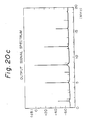
- Figure 21a is a view showing a spectrum of an input waveform of a semiconductor delay circuit device
- Fig. 20b is a view showing a spectrum of an output wave-form of a previously-proposed type delay circuit device
- Fig. 20c is a view showing a spectrum of an output wave-form of a semiconductor delay circuit device embodying the present invention.
- the input signal is a frequency modulated wave
- a carrier of the input signal is at 8.5 MHz
- a modulation signal of the input signal is at 3.58 MHz.
- the proposed semiconductor delay circuit device has a common source region such as shown in Figs. 13, 17, and the like
- the semiconductor delay circuit device of the present embodiment has a substrate contact diffusion region and separated source regions such as shown in Figs. 14, 18, and the like.
- an input signal of a semiconductor delay circuit device has some peaks at about 1.3 MHz, 4.9 MHz, 8.5 MHz, 12.1 MHz, and 15.7 MHz.
- an output signal which is delayed and output from the previously-proposed type delay circuit device has a plurality of peaks. These peaks of the output signal from the proposed semiconductor delay circuit device include the peaks of the input signal, but other peaks are also included in the output signal. Conversely, as shown in Fig. 20c, an output signal which is delayed and output from the semiconductor delay circuit device of the present embodiment is near-identical to the input signal shown in Fig. 20a. Namely, comparing the spectrum of Fig. 20c with that of Fig.
- the output signal of the present semiconductor delay circuit device includes few extraneous peaks, since the semiconductor delay circuit device of the present embodiment has a substrate contact diffusion region which is provided between the source regions of a pair of the same conduction type transistors and has the effect that operation current flowing to one transistor never influences a source potential of the other transistor of the pair transistors which are arranged adjacent to each other and facing each other.
- each row is 4, e.g., the first row, comprises the inverters I1′ to I4′.
- Each (for example I1′) of the inverters is constituted as a CMOS inverter circuit comprising a P-channel transistor Qp and an N-channel transistor Qn as shown in Fig. 22.
- Figure 23 shows changing states of an output signal waveform in each of the multiple stage inverter circuits shown in Fig. 21 when an input signal indicated with 1 (a high level portion and a low level portion having the same width, i.e., its duty ratio being 50%) is input into the first stage inverter I′,.
- ⁇ current gain
- ⁇ of the P-channel transistor inverse proportion to ON resistance of the transistor
- ⁇ of the P-channel transistor is inevitably smaller than ⁇ of the N-channel transistor due to the difference of mobility of carriers of the transistors.
- an output waveform 2 of the inverter I′ is explained.
- a fall of the same is delayed by a predetermined time t behind a rise of the waveform 1 and it abruptly falls at that time. Since ⁇ of the P-channel transistor is low, the waveform 2 gently rises at a time delayed by the predetermined time t after a fall of the waveform 1 so that its rising waveform may be obtuse (gradual).
- an output waveform 3 of the inverter I2 is explained.
- the waveforms gently rises at a time delayed by the predetermined time t after the fall of the waveform 2, and abruptly falls at a time delayed by the predetermined time t behind an intermediate level point of a rise portion of the waveform 2. Accordingly, a duty ratio of the output waveform 3 of the inverter I2 in the second stage (even stage) again becomes the original duty ratio.
- an output waveform 4 of the inverter I3′ is explained. It abruptly falls at a time delayed by the predetermined time t behind an intermediate level point of the rise portion of the waveform 3, and it obtusely rises at a time delayed by the predetermined time t after the fall of the waveform 3.
- an output waveform 5 of the inverter I4′ is explained. Since an output wiring of the inverter I4′ is turned and connected to an input of the inverter I5′ of the next row (second row), the length and area thereof may be extended. Therefore, its wiring capacity increases causing a large load so that its rising waveform becomes extremely obtuse and large (its rise time being delayed by t after the fall of the waveform 4). Its falling waveform also becomes slightly obtuse.
- the waveform 5 compared to the first input waveform 1, the waveform 5 largely influences a reduction of duty ratio of a high level side, particularly the rising portion of the waveform 1 (i.e., the first cycle of the waveform 1) becomes drastically obtuse.
- an output waveform 6 of the inverter I5′ falls at a time delayed by t behind an intermediate level point of the rising portion of the waveform 5, and obtusely rises at a time delayed by t behind an intermediate level point of the falling portion of the waveform 5.
- An output waveform 7 of last stage inverter I8′ of the second row rises quite obtusely similar to the waveform 5 and falls slightly obtusely for the same reason mentioned above, because an output of the inverter I8′ is turned and connected to an input of the inverter I9′.
- the rising portion of the first input waveform 1 (the first cycle of the waveform 1) becomes quite obtuse, and the waveform 7 is affected in a manner similar to that in the waveform 5 so that its duty ratio on the high level side may further decrease.
- output waveforms 8 and 9 of inverters I9′ and I10′ in the third row will be as shown in the figure.
- the duty ratio gradually changes from the first duty ratio (50%).
- each row contains an even number of inverters, and an output of one row is turned and connected to the next row.
- An output waveform of the last stage inverter of each row (I4′ or I8′ in the above example) becomes quite obtuse (affected greatly) always on the same side with respect to the signal waveform 1 input into the first stage inverter I1′ (i.e., always on the rising side of the above example). Accordingly, as the number of turning rows increases, the duty ratio of an output waveform gradually changes from the duty ratio of the first input waveform 1 (causing secondary harmonic distortion). Finally, a problem is caused that a waveform on the high level or low level side almost disappears.
- ⁇ of a P-channel transistor is smaller than ⁇ of an N-channel transistor in each inverter. If ⁇ of the P-channel transistor is larger than ⁇ of the N-channel transistor, for example, a layout pattern of the P-channel transistor is larger than a layout pattern of the N-channel transistor, an output waveform of the last stage inverter of each row is greatly affected always on the same side (on the falling side in this case with respect to the signal waveform 1 input into the first stage inverter I1′, thus causing the same problem as above.
- Figure 24 shows a semiconductor delay circuit device having multistage inverter circuits on a chip C according to an embodiment of the present invention.
- the multistage inverter circuits are sequentially turned (two times) to form three rows, and are cascade-connected.
- the number of inverter circuits in each row is made odd (three in this case).
- each inverter is constituted as a CMOS inverter circuit comprising a P-channel transistor and an N-channel transistor.
- Figure 25 shows waveforms of respective portions of the multistage inverter circuits shown in Fig. 24. Similar to the case of Fig. 23, 1 indicates an input signal waveform with a duty ratio of 50% input in a first stage inverter I1. In each inverter, it is supposed that ⁇ of the P-channel transistor is smaller than ⁇ of the N-channel transistor.
- an output waveform 2 of the inverter 11 and an output waveform 3 will be the same as those of Fig. 23. Since the output wiring of an inverter I3 in the last stage of the first row is turned and connected to the input of an inverter I4 of the next row (second row), an output waveform 4 of the inverter I3 rises quite obtusely and falls slightly obtusely for the same reasons explained with reference to Fig. 23. In this case, its rising point is delayed by a time t behind a falling point of the waveform 3, and its falling point is delayed by t behind an intermediate level point of a rising portion of the waveform 3.
- the waveform 4 causes a variation in the duty ratio (a reduction of the duty ratio on the high level side) because the falling portion of the waveform 1 (i.e., the second cycle of the waveform 1) becomes quite obtuse.
- output wave forms 5 and 6 of inverters I4 and I5 in the second row are sequentially delayed by the predetermined time t to become those shown in Fig 25. Since the output of an inverter I6 in the last stage of the second row is turned and connected to the input of an inverter I7 of the next row (third row), an output waveform 7 of the inverter I6 rises quite obtusely and falls slightly obtusely for the same reasons mentioned above.
- the rising portion of the waveform 1 (i.e., the first cycle of the waveform 1) becomes greatly obtuse in the waveform 7) to compensate a variation in the duty ratio in the waveform 4.
- an output waveform of the last stage inverter in each row with respect to the first input waveform 1 becomes such that portions corresponding to the falling and rising portions of the waveform 1 are alternately affected with the same influence.
- a duty ratio of an output waveform of the last stage inverter (for example I6) in an even row whose output side is connected to a turned wiring is always equal to the duty ratio of the first input waveform 1 (50% in this case).
- ⁇ of the P-channel transistor was smaller than ⁇ of the N-channel transistor in each inverter.
- ⁇ of the P-channel transistor is larger than ⁇ of the N-channel transistor, the same effect as mentioned above will be provided.
- Figure 26 shows a layout pattern of wiring to a next stage inverter in the multistage inverter circuits shown in Fig. 24.
- V-shape wiring (indicated with a numeral 211) shown in the right row is aluminum wiring for connecting two adjacent inverters in the above-mentioned first row, for example, with each other (i.e., connecting an output of the previous stage inverter with an input of the next stage inverter).
- Numeral 212 is aluminum wiring having a turning portion for connecting, for example, an output of the last stage inverter of the first row with an input of the first stage inverter of the second row.
- Numeral 213 is aluminum wiring for connecting, for example, two adjacent inverters in the second row with each other.
- the wiring length and layout area of the aluminum wiring 212 having the turning portion (corresponding to turning wiring for connecting the inverters I3 and I4 or I6 and I7 of the adjacent rows) become larger than those of the aluminum wirings 211 and 213 for connecting inverters of the same row, as shown in Fig. 26.
- numerals 221 and 222 are polysilicon layers having gate electrodes of P-channel and N-channel transistors constituting each inverter; 231 is aluminum wiring for power source connection disposed on the source region side of P-channel transistor of each inverter; 232 is aluminum wiring for power source connection disposed on the source region side of N-channel transistor of each inverter; 241 and 251 are contacts for connecting source regions of P-channel transistors of respective inverters with the aluminum wiring 231; 242 and 252 are contacts for connecting drain regions of P-channel transistors of respective inverters with the aluminum wiring 211, 212 or 213; 243 and 253 are contacts for connecting drain regions of N-channel transistors of respective inverters with the aluminum wiring 211, 212 or 213;254 is a contact for connecting the source region of N-channel transistor of each inverter with the aluminum wiring 232; 261, 262 and 263 are contacts for connecting the aluminum wiring 211, 212 or 213 (i.e., the output side of an invert
- a duty ratio of an output waveform of the last stage inverter may be substantially equal to a duty ratio of a signal waveform input in the first stage inverter.
Abstract
Description
- The present invention relates to a semiconductor integrated circuit device, for example to a semiconductor delay circuit device having a plurality of inverter circuits which are cascade-connected.
- A semiconductor delay circuit device is used for an optical disc system, for example, a laser disc system or a compact disc system. The semiconductor delay circuit device is used for delaying a detected signal of the optical disc system to maintain synchronization even if the center position of the optical disc is shifted. Namely, since the center position of an optical disc cannot be formed perfectly at the exact center of the disc in a production step, a semiconductor delay circuit device should be provided in the optical disc system for synchronization. Note, the semiconductor delay circuit device is, for example, constituted by a plurality of inverter circuits which are cascade-connected, and an input signal of the semiconductor delay circuit device is delayed in accordance with a value of a power supply voltage applied to the plurality of inverter circuits in the semiconductor delay circuit device.
- Recently, the layout pattern of proposed semiconductor delay circuit devices tends to be increasingly miniaturized by a requirement of large scale integration, and thus, inverter circuits are arranged adjacent to one another. The same conduction type (P-channel type or N-channel type) transistors of the plurality of inverter circuits in the semiconductor delay circuit device are then arranged such that their source regions are integrally formed with each other to constitute a common source region. In this case, a substrate contact diffusion region, which is an N⁺ layer or P⁺ layer that is an opposite conduction type relative to the common source region and has a higher impurity density than a substrate, is arranged for the common source region separately from the common source region. The common source region and substrate contact diffusion region are connected to power sources through aluminum wirings.
- However, when a specific transistor is operating with the above arrangement, an operation current of the transistor flows to an aluminum wiring through the common source region, that is, the operation current of the transistor does not flow only through a source region, which is the common source region, of the specific transistor, but also flows through a source region, which is also the common source region, of a transistor neighboring the specific transistor. Then, due to contact resistance between the common source region and the aluminum wiring, etc., source potentials of the specific and neighboring transistors which have the common source region may be influenced by each other.
- Further, in the layout pattern of the proposed semiconductor delay circuit device, lines that connect the respective source and drain regions of the P-channel type and N-channel type transistors run in parallel with each other, and a polysilicon layer constituting a gate electrode and an aluminum wiring for connecting the drain region of the respective transistor are constituted by combining linear portions. Therefore, a pattern forming a single inverter circuit may have many useless portions making the overall pattern larger. Additionally, in the layout pattern of the proposed semiconductor delay circuit device, as the number of turning rows increases, the duty ratio of an output waveform gradually changes from the duty ratio of a first input waveform. These problems in the proposed semiconductor delay circuit device will be described later in detail with reference to the accompanying drawings.
- An embodiment of the present invention may provide a semiconductor integrated circuit device having an effect where operation current flowing to one transistor never influences a source potential of another transistor adjacent to and facing the first transistor. Further, an embodiment of the present invention may provide a semiconductor integrated circuit device having a miniaturized pattern and a reduced layout area made as small as possible. Additionally, an embodiment of the present invention may provide a semiconductor integrated circuit device having an output waveform duty ratio equal to that of a first input waveform.
- According to the present invention, there is provided a semiconductor integrated circuit device comprising a pair of transistors of the same conduction type having source regions receiving a common power supply voltage, the source regions being arranged adjacent to each other and facing each other; and a substrate contact diffusion region whose conduction type is opposite to that of the source regions, the substrate contact diffusion region extending between the source regions. Therefore, the source regions do not influence each other.
- The semiconductor integrated circuit device may comprise a plurality of pairs of the same conduction type transistors. A substrate contact diffusion region may extend to respective source regions of the pairs of transistors in adjacent stages and protruding to approach channel forming regions of the transistors having the respective source regions.
- Further, an embodiment of the present invention may provide a semiconductor integrated circuit device comprising a first power supply line, a second power supply line, and a plurality of inverter circuits. The inverter circuits are cascade-connected and each of the inverter circuits is connected to the first and second power supply lines. Each of the inverter circuits is constituted by a first conduction type transistor and a second conduction type transistor. A pair of transistors of the same conduction type has source regions that are arranged adjacent to each other and facing each other. The conduction type of the substrate contact diffusion region is opposite to that of the source regions and which has higher impurity density than the substrate.
- The substrate contact diffusion region may have a higher impurity density than the substrate. The first conduction type transistor may be a P-channel type transistor and the second conduction type transistor may be an N-channel type transistor, and the first power supply line may be used for applying a high potential power supply to a source region of each P-channel type transistor of the inverter circuits and the second power supply line may be used for applying a low potential power supply to a source region of each N-channel type transistor of the inverter circuits.
- The substrate contact diffusion region between the source regions of the pair of transistors may include a contact portion for connecting aluminum wiring. The distance of the substrate contact diffusion region between the source regions of the pair of transistors may be less than the minimum width of diffusion. The distance of the substrate contact diffusion region between the source regions of the pair of transistors may be less than 4 microns.
- The plurality of inverter circuits may be arranged in plural rows, sequentially turned an even number of times and cascade-connected, the number of stages of the inverter circuits in each row may be odd. the number of stages of the inverter circuits in the last row may be even. An ON resistance value of the first conduction type transistor may differ from that of the second conduction type transistor.
- Additionally, an embodiment of the present invention may provide a semiconductor integrated circuit device comprising a first power supply line, a second power supply line, and a plurality of inverter circuits. The inverter circuits are cascade-connected and each of the inverter circuits is connected to the first and second power supply lines, and each of the inverter circuits is constituted by a first conduction type transistor and a second conduction type transistor.
- Source and drain regions of the first and second conduction type transistors are arranged so that extensions of lines connecting the respective source and drain regions of the first and second conduction type transistors intersect each other, and a conductive layer having gate electrodes is disposed orthogonal to the source and drain regions.
- A plan shape of a wiring contact provided for each of the source and drain regions of the first and second conduction type transistors may be hexagonal. The wiring for connecting the drain regions of the first and second conduction type transistors with each other may be curved opposite to a curve of the conductive layer having the gate electrodes of the first and second conduction type transactors. The wiring for connecting the drain regions of the first and second conduction type transistors with each other may be connected to a conductive layer having respective gate electrodes of an inverter circuit of the next stage.
- Reference is made, by way of example, to the accompanying drawings in which:-
- Figure 1 is a plan view showing a layout of a single inverter portion of a proposed semiconductor delay circuit device;
- Fig. 2 is a sectional view showing the single inverter portion of the semiconductor delay circuit device shown in Fig. 1;
- Fig 3 is an equivalent circuit view showing the single inverter portion of the semiconductor delay circuit device shown Fig. 1;
- Fig. 4 is a block diagram showing an optical disc system as an example of using the semiconductor delay circuit device;
- Fig. 5 is a circuit view showing the semiconductor delay circuit device shown in Fig. 4;
- Fig. 6 is a plan view showing a layout of a semiconductor delay circuit device according to a first embodiment of the present invention;
- Fig. 7 is a plan view showing a layout of the semiconductor delay circuit device of Fig. 6 with a first aluminum wiring layer emphasized;
- Fig. 8 is a plan view showing a layout of the semiconductor delay circuit device of Fig. 6 with contacts between the first and second a aluminum wiring layers emphasized;
- Fig. 9 is a plan view showing a layout of the semiconductor delay circuit device of Fig. 6 with the first and second aluminum wiring layers emphasized;
- Fig. 10 is an equivalent circuit view showing one inverter portion of the semiconductor delay circuit device shown in Fig. 8;
- Fig. 11 is a sectional view showing the semiconductor delay circuit device taken along a line A-A of Fig. 8;
- Fig. 12 is a sectional view showing the semiconductor delay circuit device taken along a line B-B of Fig. 8;
- Fig. 13 is a sectional view showing a part of the semiconductor delay circuit device according to a prior proposal;
- Fig. 14 is a sectional view showing a part of the semiconductor delay circuit device embodying the present invention;
- Fig. 15 a circuit view showing the semiconductor delay circuit device embodying the present invention;
- Fig. 16 is view showing the details of a connection portion between inverter columns shown in Fig. 15;
- Fig. 17 is a plan view showing a layout of a semiconductor delay circuit device according to a prior proposal;
- Fig. 18 is a plan view showing a layout of a semiconductor delay circuit device according to a second embodiment of the present invention;
- Fig. 19 is a plan view showing a layout of the semiconductor delay circuit device of Fig. 18 with aluminum wiring layers emphasized;
- Fig. 20a is a graph showing a spectrum of an input waveform of a semiconductor delay circuit device;
- Fig. 20b is a graph showing a spectrum of an output waveform of a semiconductor delay circuit device according to a prior proposal;
- Fig. 20c is a graph showing a spectrum of an output waveform of a semiconductor delay circuit device embodying the present invention;
- Fig. 21 is a view showing an arrangement of a multistage inverter circuit in a semiconductor delay circuit device according to a prior proposal;
- Fig. 22 is a circuit view showing the arrangement of each inverter circuit of Fig. 21;
- Fig. 23 is a diagram for explaining input and output waveforms of respective points of the multistage inverter circuit of Fig. 21;
- Fig. 24 is a view showing an arrangement of a multistage inverter circuit in a semiconductor delay circuit device as a variation of the embodiments according to the present invention;
- Fig. 25 is a diagram for explaining input and output waveforms of respective points of the multistage inverter circuit of Fig. 24; and
- Fig. 26 is a plan view showing an arrangement of a part of the multistage inverter circuit shown in Fig. 24.
- For a better understanding of the preferred embodiments of the present invention, the problems of the related art will be explained first.
- Figure 1 is a plan view showing a layout of a single inverter portion of a semiconductor delay circuit device in a prior proposal. The semiconductor delay circuit device is used for an optical disc system, and is used for delaying a detected signal of the optical disc system to maintain synchronization, even if a center position of the optical disc is shifted. Namely, since the center position of the optical disc cannot be formed perfectly at the exact center of the disc in a production step, a semiconductor delay circuit device should be provided in the optical disc system for synchronization. Note, the semiconductor delay circuit device is, for example, constituted by a plurality of inverter circuits which are cascade-connected, and an input signal of the semiconductor delay circuit device is delayed in accordance with a value of a power supply voltage applied to the plurality of inverter circuits in the semiconductor delay circuit device.
- As shown in Fig. 1, an N-channel transistor Qn′ and a P-channel transistor Qp′ constitute the inverter circuit. Figure 2 is a sectional view showing the single inverter portion of the semiconductor delay circuit device shown in Fig. 1. In a P⁻-
type semiconductor substrate 11′, the N-channel transistor Qn′ comprises an N⁺ diffusion layer acting as asource diffusion region 21′ and adrain diffusion region 22′. Adjacent to thesource diffusion region 21′, there is a P⁺ diffusion layer acting as a substratecontact diffusion region 31′. Thenumeral 4′, is a polysilicon layer acting as a common gate electrode with respect to the N-channel transistor Qn′ and P-channel transistor Qp′ (which is not shown in Fig. 2). The numeral 41′ is an aluminum wire for input signals connected to thepolysilicon layer 4′. Thenumeral 5′ is an aluminum wire connected to thesource diffusion region 21′ and substratecontact diffusion region 31′ atrespective contact portions 51′ and 52′. Thealuminum wire 5′ is, for example, connected to a low potential power source Vss. Thenumeral 6′ is an aluminum wire connecting thedrain diffusion region 22′ of the N-channel transistor Qn′ to a drain diffusion region (P⁺ layer) 23′ of the P-channel transistor Qp′ atrespective contact portions 61′ and 62′. Through thealuminum wire 6′, output signals of the inverter circuit are picked up. On the other hand, a source diffusion region (P⁺ layer) 24′ and a substrate contact diffusion region (N⁺ layer) 32′ adjacent to theregion 24′ of the P-channel transistor Qp′ are connected to analuminum wire 7′ viarespective contact portions 71′ and 72′. Thealuminum wire 7′ is, for example, connected to a high potential power source Vcc. Thenumeral 8′ indicates an insulation film such as a silicon oxide film. Figure 3 is an equivalent circuit view showing the single inverter portion of the semiconductor delay circuit device shown in Fig. 1. - Figure 1 shows only the layout of the portion constituting the single inverter in the semiconductor delay circuit device. Recently such a layout pattern of a semiconductor delay circuit device tends to be increasingly miniaturized. As a result, an inverter, for example the one mentioned above, is arranged adjacent to another inverter. The same conduction type (P-channel type or N-channel type) transistors are then arranged such that their source regions are integrally formed with each other to constitute a common source region. In this case, a substrate contact diffusion layer (region), which is an N⁺ layer or P⁺ layer that is of an opposite conduction type relative to the common source region and has a higher impurity density than a substrate, is arranged for the common source region, and separately from the common source region. The common source region and substrate contact diffusion region are connected to a predetermined power source via aluminum wiring.
- However, when a transistor is operating with the above-mentioned arrangement, an operation current of the transistor flows to aluminum wiring via the above-mentioned common source region. Then, due to contact resistance between the common source region and the aluminum wiring, etc., a source potential of the other transistor having the common source region varies so that characteristics, for example, a threshold voltage, of the other transistor may be influenced.
- Embodiments of the present invention may solve such a problem. Even if source regions of a pair of the same conduction type transistors are arranged adjacent to each other and facing each other, the source regions are separated by a substrate contact diffusion region that is of an opposite conduction type relative to the source regions and has a higher impurity density than the substrate. As a result, the effect of an operation current flowing to one transistor never influences a source of the other transistor.
- Further, according to the above-mentioned layout, the lines that connect the respective source and drain regions of the P-channel and N-channel transistors run in parallel with each other. The polysilicon layer having the gate electrodes of the respective transistors and the aluminum wiring for connecting the drain regions of the respective transistors are constituted by combining linear portions. Accordingly, a pattern forming a single inverter circuit, or in other words, an area needed for the layout of the inverter circuit, may have many useless portions making the overall pattern larger.
- Therefore, when a particularly large number of inverter circuits, for example, connected in multiple stages, are provided, a problem is caused that they increase the general layout area that is the number of inverter circuits that can be arranged in a unit area is considerably limited.
- Embodiments of the invention may also solve the above problem, so that the pattern of an inverter circuit can be miniaturized and improved to reduce the layout area to be as small as possible, or to increase the number of inverter circuits to be arranged in a unit area as much as possible.
- Figure 4 is a block view showing an optical disc system for an example of using the semiconductor delay circuit device. As described above, a semiconductor delay circuit device is used for an optical disc system, and is used for delaying a detected signal of the optical disc system to maintain synchronization, even if a center position of an optical disc is shifted.
- As shown in Fig. 4, an optical disc system is basically constituted by a
pickup 401, a semiconductor delay circuit device (phase controller) 402, an FM-detection portion 403, a synchronizing signalselect portion 404, and aphase difference detector 405. Data (for example, a video signal data or an audio signal data) stored on anoptical disc 400 is picked up by thepickup 401, and an output signal of thepickup 401 is supplied to the semiconductordelay circuit device 402. An output signal of the semiconductordelay circuit device 402 is supplied to the FM-detection portion 403, and an output signal of the optical disc system, for example, a video signal or an audio signal, is output from the FM-detection portion 403. Note, a synchronizing signal is selected by the synchronizing signalselect portion 404 via the FM-detection portion 403, and the output signal of the synchronizing signalselect portion 404 is supplied to thephase difference detector 405. Thephase difference detector 405 is also supplied with a reference signal, and thephase difference detector 405 outputs a voltage control signal to the semiconductordelay circuit device 402 by comparing the synchronizing signal from the synchronizing signalselect portion 404 and the reference signal. - In the above description, the output signal of the
pickup 401 is a frequency modulated signal including a phase fluctuation of ±27 µsec., and this phase fluctuation is caused by, for example, an eccentricity of a center position in theoptical disc 400. Namely, the center position of theoptical disc 400 cannot be formed perfectly at the exact center of the disc in a production step, so the semiconductordelay circuit device 402 is used for delaying the output signal from thepickup 401 to maintain a synchronization in accordance with the voltage control signal output from thephase difference detector 405. Note, the semiconductordelay circuit device 402 is, for example, constituted by a plurality of inverter circuits which are cascade-connected, and the output signal of thepickup 401 is delayed for synchronizing by the synchronizing signal from the synchronizing signalselect portion 404 and the reference signal in accordance with a value of a power supply voltage, which is the voltage control signal, applied to the plurality of inverter circuits in the semiconductor delay circuit device. Consequently, the output signal of the optical disc system, which is the output signal of the FM-detection portion 403, is maintained in a stable state with no phase fluctuation. In the above description, a delay value of the semiconductordelay circuit device 402 is determined to be a value larger than the phase fluctuation range (for example, ±27 µsec.) of the frequency modulated signal picked up by thepickup 401. For example, the delay value of the semiconductordelay circuit device 402 is determined to be 60 µsec. - Figure 5 is a circuit view showing the semiconductor delay circuit device shown in Fig. 4. As shown in Fig. 5, the semiconductor
delay circuit device 402 is constituted by a plurality of inverter circuits I₁ , I₂ , I₃ , ... , In-1 , In , In+1 , ... For example, the semiconductordelay circuit device 402 is constituted by a plurality of rows R₁ , R₂ , R₃ , ... with each of the rows including a few hundred inverters, and the semiconductordelay circuit device 402 is constituted by 24000 stages of inverter circuits which are cascade-connected. - Next, preferred embodiments of the present invention will be described.
- Below, some embodiments of a semiconductor delay circuit device according to the present invention will be explained with reference to the drawings.
- Figures 6 to 8 show a layout of a semiconductor delay circuit device according to an embodiment of the present invention. In the semiconductor delay circuit device, multistage inverter circuits, which comprise P-channel transistors and N-channel transistors, are cascade-connected. Namely, wiring (aluminum wiring) for connecting respective drain regions of a predetermined inverter circuit is connected to a conductive layer, for example, a polysilicon layer, having respective gate electrodes of an inverter circuit of the next stage. In this way, many inverters are successively connected in multiple stages, for example, 24000 stages, and in multiple columms to form a delay circuit, etc.
- Figure 6 shows a layout pattern including source and drain diffusion regions of the P-channel transistors and N-channel transistors that constitute inverter circuits, polysilicon layers having gate electrodes of the respective transistors, and substrate (power source) contact diffusion layers (regions) that are arranged between respective source regions of the P-channel transistors constituting adjacent inverters and between respective source regions of the N-channel transistors constituting adjacent inverters.
- Namely, in Fig. 6,
numerals Numerals Numeral 51 is a polysilicon layer. Bothedge portions 51′ and 52˝ of the polysilicon layer function as gate electrodes of the P-channel transistor and N-channel transistor.Numeral 52 is a polysilicon layer having gate electrodes of respective transistors constituting an inverter of the next stage. Thepolysilicon layer 52 is connected to aluminum wiring which is indicated as a firstlayer aluminum wiring 62 in Figs. 7, 8 and 11, for connecting thedrain regions Numerals 62′, 62˝ and 62‴ are aluminum contacts, for example, refer to Fig. 11, for connecting thealuminum wiring 62 to thedrain regions polysilicon layer 52. -
Numerals contact diffusion region 31 is arranged to interpose between thesource regions region 31, i.e., a facing distance of thesource regions Numerals 22′ and 53˝ are a drain region and a gate electrode, respectively, of the P-channel transistor constituting the inverter of the adjacent column . On the other hand, the substratecontact diffusion region 32 is arranged to interpose between the source regions of the P-channel transistors constituting inverters of consecutive stages. Each edge portion of theregion 32 protrudes to approach a channel forming region, which is a portion just under agate electrode 51′, of a transistor having the corresponding source region, for example, the P-channel transistor having thesource region 21.Numerals 61′, 61˝ and 32′ are aluminum contacts for connecting thesource regions substrate diffusion regions layer aluminum wiring 61 in Figs. 7, 8 and 11. - Similarly,
numerals region 41 is arranged to interpose between thesource regions region 41, i.e., a facing distance between thesource regions Numerals 24′ and 54˝ are a drain region and a gate electrode, respectively, of the N-channel transistor constituting each of the inverters of the adjacent columns. On the other hand, theregion 42 is arranged to interpose between the source regions of the N-channel transistors constituting inverters of adjacent stages. Each edge portion of theregion 42 protrudes to approach a channel forming region, which is a portion just under agate electrode 51˝, of the transistor having the corresponding source region, for example, the N-channel transistor having thesource region 23.Numerals 63′, 63˝ and 42′ are aluminum contacts for connecting thesource regions contact diffusion regions layer aluminum wiring 63 in Figs. 7, 8 and 11. - Figure 7 shows, in addition to the layout pattern shown in Fig. 6, a layout pattern of the first layer aluminum wiring. As shown in Fig. 7, the
aluminum wiring 62 for connecting the drain regions of respective transistors constituting a predetermined inverter with a polysilicon layer has gate electrodes of an inverter of the next stage, thealuminum wiring 61 for connecting the respective source regions of P-channel transistors constituting respective inverters with the substrate contact diffusion regions (N⁺ layers) is disposed between the source regions, and thealuminum wiring 63 for connecting the source regions of N-channel transistors of respective inverters with the substrate contact diffusion regions (P⁺ layers) is disposed between the source regions. Figure 8 shows, in addition to the respective layout patterns shown in Fig. 7, a layout pattern of analuminum contact 71′ for connecting the firstlayer aluminum wiring 61 with a secondlayer aluminum wiring 71, for example, refer to Figs. 9 and 11, and analuminum contact 72′ for connecting thefirst aluminum wiring 63 with analuminum wiring 72, for example, refer to Figs. 9 and 11. Figure 9 shows a layout pattern of the firstlayer aluminum wirings layer aluminum wirings - Figure 10 shows an equivalent circuit of a single inverter portion of the layout pattern shown in Fig. 8. A reference mark Qp indicates a P-channel transistor and Qn an N-channel transistor. Figures 11 and 12 are sectional views showing the semiconductor delay circuit device, taken along a line A-A and a line B-B of Fig. 8, respectively. In Figs. 11 and 12, numeral 11 is a P⁻-type semiconductor substrate, 12 an N⁻-type well, 8 a field oxide film, and 9 an interlayer insulation film.
- Figure 13 is a sectional view showing a part of the semiconductor delay circuit device according to a prior proposal , and Figure 14 is a sectional view showing a part of the semiconductor delay circuit device embodying the present invention.
- As shown in Fig. 13, in the previously-proposed type delay circuit device, two P-channel transistors Qp₁ and Qp₂ , whose source regions are commonly formed as a
common source region 21a of the proposed semiconductor delay circuit device, influence each other by way of thecommon source region 21a. - Namely, when the P-channel transistor Qp₁ is operating and a current flows from
aluminum wiring 61 via thecommon source region 21a to adrain region 22′, the current flowing to thedrain region 22′ of the transistors Qp₁ does not only flow from thealuminum wiring 61 passing through analuminum contact 61˝ and thecommon source region 21a (which is shown by a reference i₀₁′ in Fig. 13), but also flows from thealuminum wiring 61 passing through analuminum contact 61′ and thecommon source region 21a (which is shown by a reference i₀₂′ in Fig. 13). - Similarly when the P-channel transistor Qp₂ is operating and a current flows from the
aluminum wiring 61 via thecommon source region 21a to adrain region 22, the current flowing to thedrain region 22 of the transistors Qp₂ does not only flow from thealuminum wiring 61 passing through thealuminum contact 61′ and thecommon source region 21a (which is shown by a reference i₀₁ in Fig. 13), but also flows from thealuminum wiring 61 passing through thealuminum contact 61˝ and thecommon source region 21a (which is shown by a reference i₀₂ in Fig. 13). Note, the above pair of transistors of the same conduction type are arranged adjacent to each other and facing each other, and the semiconductor delay circuit device comprises a plurality of pairs of the same conduction type transistors. Therefore, an input signal of the semiconductor delay circuit, for example, an output signal of a pickup in an optical disc system, is distorted. - Conversely, as shown in Fig. 14, in the semiconductor delay circuit device of the present embodiment,
source regions 21′ and 21 of two P-channel transistors Qp₁ and Qp₂ are formed separately by a substratecontact diffusion region 31. Note, a conduction type of the substratecontact diffusion region 31 is opposite to that of thesource regions contact diffusion region 31 is an N-channel type (N⁺ diffusion layer) and each of thesource regions contact diffusion region 31. Therefore, the P-channel transistors Qp₁ and Qp₂ are not influenced by each other. - Namely, when the P-channel transistor Qp₁ is operating and a current flows from
aluminum wiring 61 to adrain region 22′, the current flowing to thedrain region 22′ of the transistors Qp₁ only flows from thealuminum wiring 61 passing through analuminum contact 61˝ and thesource region 21′ (which is shown by a reference i₀₁′ in Fig. 14), and the current never flows from thealuminum wiring 61 passing through analuminum contact 61′, thesource region contact diffusion region 31. - Similarly, when the P-channel transistor Qp₂ is operating and a current flows from
aluminum wiring 61 to adrain region 22, the current flowing to thedrain region 22 of the transistors Qp₂ only flows from thealuminum wiring 61 passing through analuminum contact 61′ and the source region 21 (which is shown by a reference i₀₁ in Fig. 14), and the current never flows from thealuminum wiring 61 passing through analuminum contact 61˝ and thesource region 21′, 21 and the substrate contact diffusion region 31 (which is shown by a reference i₀₂ in Fig. 14), since the current i₀₂ is blocked by the substratecontact diffusion region 31. - As described above, the semiconductor delay circuit device of the present embodiment has the effect that operation current flowing to one transistor never influences a source potential of the other transistor adjacent to and facing the first transistor.
- Figure 15 shows an equivalent circuit of the semiconductor delay circuit device employing the present invention, in which numerals I₁ to I₇ indicate inverters and "C" an IC chip. Figure 16 shows the details of a connection portion between inverter columns shown in Fig. 15. The connection portion between inverters of adjacent columns is indicated with a numeral 64. Other reference marks are common to those shown in the other figures.
- As described in the above, according to the present embodiment, the source and drain
regions regions regions gate electrodes 51′ and 52˝ are orthogonal to a line connecting the source and drainregions regions aluminum wiring 62 for connecting thedrain regions polysilicon layer 51. Namely, according to the present embodiment, a layout pattern of the respective component elements of single CMOS inverter circuit is constituted as mentioned above. Due to this, an area needed for the layout is fully reduced in both longitudinal and lateral directions. As a result, the number of inverters to be arranged in a limited chip area can drastically be increased. - In addition to the layout pattern of the respective component elements mentioned above, the aluminum contacts, for instance, 61 and 63′, for the
aluminum wiring aluminum wiring 62 provided for the respective drain regions and polysilicon layers may each be formed with a hexagonal shape. Compared to an aluminum contact having the same contact area but a rectangular shape, the hexagonal contact can reduce the distance between adjacent aluminum contacts. Note, a design criterion related to the distance between the contacts is mainly determined according to a distance between protruding portions thereof. By combining the above-mentioned layout pattern with the hexagonal aluminum contacts, an overall layout area can effectively be miniaturized. - The reason why the substrate
contact diffusion regions - First, the substrate contact diffusion region 32 (N⁺ layer) disposed between the source regions of P-channel transistors and the substrate contact diffusion region 42 (P⁺ layer) disposed between the source regions of N-channel transistors forming the inverters of adjacent stages are projectingly formed as mentioned above to approach the channel forming regions of the transistors having corresponding source regions. For example, they are projectingly formed to approach the channel forming regions, which are portions just under the
gate electrodes 51′, of the P-channel transistors having thesource regions 21, and the channel forming regions, which are portions just under thegate electrodes 51˝, of the N-channel transistors having thesource regions 23. Thesubstrate contacts substrate contacts diffusion regions diffusion regions - As the layout pattern of each inverter is miniaturized as mentioned above, transistors constituting respective inverters are closer to each other. Therefore, when a column of transistors sequentially connected in multiple stages (in the longitudinal direction of the figures) as mentioned above returns at a predetermined position to form an adjacent transistor column ,
respective source regions source regions source regions source region 21, may flow to aluminum wiring via a common source region so that a source potential of thesource region 21′ of the other transistor may vary due to contact resistance, etc., between the source region and the aluminum wiring. As a result, the characteristics such as threshold voltage of the adjacent column transistor having thesource region 21′ may be affected. - However, according to the present embodiment, although the source regions of transistors in the adjacent columns are arranged to face each other in the length direction as mentioned above, the N⁺
diffusion layer 31 and P⁺diffusion layer 41 each of narrow width to separate all the source regions of adjacent transistors, are arranged between thesource regions source regions - Namely, even if adjacent source regions are closely positioned, the source regions are separated by the substrate contact diffusion region comprising the N⁺ layer or P⁺ layer of opposite conduction type relative to the source regions and of higher impurity density than a substrate. This is why the present invention provides the contact diffusion region. In this case, the width of the contact diffusion region, i.e., a distance between the facing source regions, may be made narrower than the minimum length of a channel formed in the P-channel transistor or in the N-channel transistor, as mentioned above.
- It is preferable that the distance between the source regions that are separated as mentioned above be less than 4 microns, and the distance between the source regions be less than the minimum width of diffusion.
- Figure 17 is a plan view showing a layout of a semiconductor delay circuit device of a prior proposal, and Fig. 18 is a plan view showing a layout of a semiconductor delay circuit device according to a second embodiment of the present invention. Note, the semiconductor delay circuit device of Fig. 18 corresponds to the proposed semiconductor delay circuit device of Fig. 17. Comparing the semiconductor delay circuit devices shown in Figs. 17 and 18, the semiconductor delay circuit device of Fig. 17 has a
common source region 121a, and the semiconductor delay circuit device of the present embodiment (Fig. 18) has a separatedsource region source regions source regions - The semiconductor delay circuit device of the present embodiment is similar to the embodiment shown in Figs. 6 to 12, and the semiconductor delay circuit device comprises a plurality of inverter circuits which comprise P-channel transistors and N-channel transistors and are cascade-connected in plural columms.
- In Fig. 18
numerals source regions 121 of the P-channel transistor and asource region 121′ of a P-channel transistor that is in the next column and adjacent to thesource region 121 to face thesource region 121. The substrate contact diffusion region 131 corresponds to the substratecontact diffusion region 31 of the first embodiment mentioned in the above.Numeral 132 is a substrate contact diffusion region (N⁺ layer) disposed between source regions of P-channel transistors that constitute inverters of adjacent stages, and corresponds to the substratecontact diffusion region 32 of the first embodiment. Similar to thediffusion region 32, the substratecontact diffusion region 132 protrudes to approach channel forming regions, for example, portions just under agate electrode 151′, of the P-channel transistors. - On the other hand, numeral 141 is a substrate contact diffusion region (P⁺ layer) disposed between the
source region 123 of the N-channel transistor and a source region of an N-channel transistor that is positioned adjacent to thesource region 123 and face thesource region 123. The substratecontact diffusion region 141 corresponds to the substratecontact diffusion region 41 of the first embodiment. Further, numeral 142 is a substrate contact diffusion region (P⁺ layer) disposed between source regions of N-channel transistors that constitute inverters of adjacent stages, and corresponds to the substratecontact diffusion region 42 of the embodiment shown in Figs. 6 to 12. Similar to thediffusion region 42, the substratecontact diffusion region 142 protrudes to approach channel forming regions, for example, a portion just under agate electrode 151˝, of the N-channel transistors. -
Numeral 151 is a polysilicon layer both ends of which havegate electrodes 151′ and 151˝. A numeral 152 is a similar polysilicon layer disposed for an inverter of the next stage. - Figure 19 shows layout patterns of
aluminum wirings aluminum wirings drain regions -
Numerals 161′, 161˝ and 132′ are contacts for connecting thesource regions contact diffusion regions 131 and 132 with thealuminum wiring 161.Numerals 162′, 162˝ and 162‴ are contacts for connecting thedrain region 122 of P-channel transistor, thedrain region 124 of N-channel transistor and thepolysilicon layer 152 respectively to thealuminum wiring 162.Numerals 163′ and 142′ are contacts for connecting thesource region 123 of N-channel transistor and the substratecontact diffusion regions source region 123 to face thesource region 123 being naturally connected to the aluminum wiring 163). - In this embodiment also, the substrate
contact diffusion regions regions - According to the present embodiment, even if source regions of same conduction type transistors are arranged adjacent to each other and facing each other, an effect of operation current flowing to one transistor never influences a source potential of the other transistor adjacent to and facing the first transistor. Therefore, characteristics, for example, a threshold voltage, of the other transistor can be surely prevented from varying.
- Figure 21a is a view showing a spectrum of an input waveform of a semiconductor delay circuit device, Fig. 20b is a view showing a spectrum of an output wave-form of a previously-proposed type delay circuit device, and Fig. 20c is a view showing a spectrum of an output wave-form of a semiconductor delay circuit device embodying the present invention.
- Note, the input signal is a frequency modulated wave, a carrier of the input signal is at 8.5 MHz, and a modulation signal of the input signal is at 3.58 MHz. Further, the proposed semiconductor delay circuit device has a common source region such as shown in Figs. 13, 17, and the like, and the semiconductor delay circuit device of the present embodiment has a substrate contact diffusion region and separated source regions such as shown in Figs. 14, 18, and the like.
- As shown in Fig. 20a, an input signal of a semiconductor delay circuit device has some peaks at about 1.3 MHz, 4.9 MHz, 8.5 MHz, 12.1 MHz, and 15.7 MHz.
- As shown in Fig. 20b, an output signal which is delayed and output from the previously-proposed type delay circuit device has a plurality of peaks. These peaks of the output signal from the proposed semiconductor delay circuit device include the peaks of the input signal, but other peaks are also included in the output signal. Conversely, as shown in Fig. 20c, an output signal which is delayed and output from the semiconductor delay circuit device of the present embodiment is near-identical to the input signal shown in Fig. 20a. Namely, comparing the spectrum of Fig. 20c with that of Fig. 20b, the output signal of the present semiconductor delay circuit device includes few extraneous peaks, since the semiconductor delay circuit device of the present embodiment has a substrate contact diffusion region which is provided between the source regions of a pair of the same conduction type transistors and has the effect that operation current flowing to one transistor never influences a source potential of the other transistor of the pair transistors which are arranged adjacent to each other and facing each other.
- Next, further embodiments of the present invention will be explained. For a better understanding of these preferred embodiments, the problems of the related art will be explained first.
- Generally, to form a semiconductor delay circuit device multiple stages (for instance, 24000 stages) of inverter circuits are arranged on a chip C. As shown in Fig. 21, multiple stages of inverters I₁′, I₂′, I₃′, ... are cascade-connected and sequentially turned to form plural rows. The number of inverter circuits in each row, i.e., the number of stages of each row, is made even. In Fig. 21, for the sake of simplicity, the number of inverter circuits in each row is 4, e.g., the first row, comprises the inverters I₁′ to I₄′. Each (for example I₁′) of the inverters is constituted as a CMOS inverter circuit comprising a P-channel transistor Qp and an N-channel transistor Qn as shown in Fig. 22.
- Figure 23 shows changing states of an output signal waveform in each of the multiple stage inverter circuits shown in Fig. 21 when an input signal indicated with ① (a high level portion and a low level portion having the same width, i.e., its duty ratio being 50%) is input into the first stage inverter I′,. Here β (current gain) of the P-channel transistor (inverse proportion to ON resistance of the transistor) of each inverter is supposed to be smaller than β of the N-channel transistor of the inverter. Generally, if the P-channel transistor and N-channel transistor have the same pattern, β of the P-channel transistor is inevitably smaller than β of the N-channel transistor due to the difference of mobility of carriers of the transistors.
- First, an
output waveform ② of the inverter I′, is explained. A fall of the same is delayed by a predetermined time t behind a rise of thewaveform ① and it abruptly falls at that time. Since β of the P-channel transistor is low, thewaveform ② gently rises at a time delayed by the predetermined time t after a fall of thewaveform ① so that its rising waveform may be obtuse (gradual). Next, anoutput waveform ③ of the inverter I₂ is explained. For the same reason, the waveforms gently rises at a time delayed by the predetermined time t after the fall of thewaveform ②, and abruptly falls at a time delayed by the predetermined time t behind an intermediate level point of a rise portion of thewaveform ②. Accordingly, a duty ratio of theoutput waveform ③ of the inverter I₂ in the second stage (even stage) again becomes the original duty ratio. Next, anoutput waveform ④ of the inverter I₃′ is explained. It abruptly falls at a time delayed by the predetermined time t behind an intermediate level point of the rise portion of thewaveform ③, and it obtusely rises at a time delayed by the predetermined time t after the fall of thewaveform ③. Further, anoutput waveform ⑤ of the inverter I₄′ is explained. Since an output wiring of the inverter I₄′ is turned and connected to an input of the inverter I₅′ of the next row (second row), the length and area thereof may be extended. Therefore, its wiring capacity increases causing a large load so that its rising waveform becomes extremely obtuse and large (its rise time being delayed by t after the fall of the waveform ④). Its falling waveform also becomes slightly obtuse. (Its falling point is delayed by t behind an intermediate level point of the rising portion of thewaveform ④.) In this way, compared to thefirst input waveform ①, thewaveform ⑤ largely influences a reduction of duty ratio of a high level side, particularly the rising portion of the waveform ① (i.e., the first cycle of the waveform ①) becomes drastically obtuse. Similarly, anoutput waveform ⑥ of the inverter I₅′ falls at a time delayed by t behind an intermediate level point of the rising portion of thewaveform ⑤, and obtusely rises at a time delayed by t behind an intermediate level point of the falling portion of thewaveform ⑤. Anoutput waveform ⑦ of last stage inverter I₈′ of the second row rises quite obtusely similar to thewaveform ⑤ and falls slightly obtusely for the same reason mentioned above, because an output of the inverter I₈′ is turned and connected to an input of the inverter I₉′. In this way, similar to thewaveform ⑤, the rising portion of the first input waveform ① (the first cycle of the waveform ①) becomes quite obtuse, and thewaveform ⑦ is affected in a manner similar to that in thewaveform ⑤ so that its duty ratio on the high level side may further decrease. In this way,output waveforms - As described above, according to the multistage inverter circuit already proposed, each row contains an even number of inverters, and an output of one row is turned and connected to the next row. An output waveform of the last stage inverter of each row (I₄′ or I₈′ in the above example) becomes quite obtuse (affected greatly) always on the same side with respect to the
signal waveform ① input into the first stage inverter I₁′ (i.e., always on the rising side of the above example). Accordingly, as the number of turning rows increases, the duty ratio of an output waveform gradually changes from the duty ratio of the first input waveform ① (causing secondary harmonic distortion). Finally, a problem is caused that a waveform on the high level or low level side almost disappears. The above explanation was given for the case that β of a P-channel transistor is smaller than β of an N-channel transistor in each inverter. If β of the P-channel transistor is larger than β of the N-channel transistor, for example, a layout pattern of the P-channel transistor is larger than a layout pattern of the N-channel transistor, an output waveform of the last stage inverter of each row is greatly affected always on the same side (on the falling side in this case with respect to thesignal waveform ① input into the first stage inverter I₁′, thus causing the same problem as above. - Below, an example of a semiconductor delay circuit device of a further embodiment will be explained with reference to Figs. 24 to 26.
- Figure 24 shows a semiconductor delay circuit device having multistage inverter circuits on a chip C according to an embodiment of the present invention. In Fig. 24, the multistage inverter circuits are sequentially turned (two times) to form three rows, and are cascade-connected. The number of inverter circuits in each row is made odd (three in this case). As shown in Fig. 22 each inverter is constituted as a CMOS inverter circuit comprising a P-channel transistor and an N-channel transistor.
- Figure 25 shows waveforms of respective portions of the multistage inverter circuits shown in Fig. 24. Similar to the case of Fig. 23, ① indicates an input signal waveform with a duty ratio of 50% input in a first stage inverter I₁. In each inverter, it is supposed that β of the P-channel transistor is smaller than β of the N-channel transistor.
- Due to this, an
output waveform ② of theinverter 1₁ and anoutput waveform ③ will be the same as those of Fig. 23. Since the output wiring of an inverter I₃ in the last stage of the first row is turned and connected to the input of an inverter I₄ of the next row (second row), anoutput waveform ④ of the inverter I₃ rises quite obtusely and falls slightly obtusely for the same reasons explained with reference to Fig. 23. In this case, its rising point is delayed by a time t behind a falling point of thewaveform ③, and its falling point is delayed by t behind an intermediate level point of a rising portion of thewaveform ③. In this way, with respect to thefirst input waveform ①, thewaveform ④ causes a variation in the duty ratio (a reduction of the duty ratio on the high level side) because the falling portion of the waveform ① (i.e., the second cycle of the waveform ①) becomes quite obtuse. Similarly, output wave forms ⑤ and ⑥ of inverters I₄ and I₅ in the second row are sequentially delayed by the predetermined time t to become those shown in Fig 25. Since the output of an inverter I₆ in the last stage of the second row is turned and connected to the input of an inverter I₇ of the next row (third row), anoutput waveform ⑦ of the inverter I₆ rises quite obtusely and falls slightly obtusely for the same reasons mentioned above. Contrary to thewaveform ④, with respect to thefirst input waveform ①, the rising portion of the waveform ① (i.e., the first cycle of the waveform ①) becomes greatly obtuse in the waveform ⑦) to compensate a variation in the duty ratio in thewaveform ④. In this way, by sequentially turning and connecting the inverters an even number of times, and by making the number of stages of inverters in each row (except the last row) odd, an output waveform of the last stage inverter in each row with respect to thefirst input waveform ① becomes such that portions corresponding to the falling and rising portions of thewaveform ① are alternately affected with the same influence. A duty ratio of an output waveform of the last stage inverter (for example I₆) in an even row whose output side is connected to a turned wiring is always equal to the duty ratio of the first input waveform ① (50% in this case). for example, the duty ratio of thewaveform ⑦ will be 50%, i.e., (t₁ = t₂), at each intermediate level point. Since an output waveform of each inverter in the last row (third row in this case) rises Slightly obtusely, a duty ratio of the output waveform of the odd inverter may slightly differ from the duty ratio of theinput waveform ①. However, at an output waveform of the next even stage inverter, its duty ratio returns to the original one. Unlike the type of circuit shown in Fig. 23, the duty ratio does not gradually change as the number of stages of inverters that are sequentially turned and connected in plural rows increases. - In the above embodiment, β of the P-channel transistor was smaller than β of the N-channel transistor in each inverter. However, even if β of the P-channel transistor is larger than β of the N-channel transistor, the same effect as mentioned above will be provided.
- Figure 26 shows a layout pattern of wiring to a next stage inverter in the multistage inverter circuits shown in Fig. 24. In Fig. 26, V-shape wiring (indicated with a numeral 211) shown in the right row is aluminum wiring for connecting two adjacent inverters in the above-mentioned first row, for example, with each other (i.e., connecting an output of the previous stage inverter with an input of the next stage inverter).
Numeral 212 is aluminum wiring having a turning portion for connecting, for example, an output of the last stage inverter of the first row with an input of the first stage inverter of the second row.Numeral 213 is aluminum wiring for connecting, for example, two adjacent inverters in the second row with each other. Namely, the wiring length and layout area of thealuminum wiring 212 having the turning portion (corresponding to turning wiring for connecting the inverters I₃ and I₄ or I₆ and I₇ of the adjacent rows) become larger than those of thealuminum wirings - In Fig. 26, numerals 221 and 222 are polysilicon layers having gate electrodes of P-channel and N-channel transistors constituting each inverter; 231 is aluminum wiring for power source connection disposed on the source region side of P-channel transistor of each inverter; 232 is aluminum wiring for power source connection disposed on the source region side of N-channel transistor of each inverter; 241 and 251 are contacts for connecting source regions of P-channel transistors of respective inverters with the aluminum wiring 231; 242 and 252 are contacts for connecting drain regions of P-channel transistors of respective inverters with the aluminum wiring 211, 212 or 213; 243 and 253 are contacts for connecting drain regions of N-channel transistors of respective inverters with the aluminum wiring 211, 212 or 213;254 is a contact for connecting the source region of N-channel transistor of each inverter with the aluminum wiring 232; 261, 262 and 263 are contacts for connecting the aluminum wiring 211, 212 or 213 (i.e., the output side of an inverter of previous stage) with an input side (polysilicon layer 221 or 222) of the next stage inverter; 271 is a contact for connecting a substrate contact diffusion region disposed on the source region side of P-channel transistor of each inverter with the aluminum wiring 231; and 272 is a contact for connecting a substrate contact diffusion region disposed on the source region side of the N-channel transistor of each inverter with the aluminum wiring 232.
- According to the present embodiment even if inverter circuits in each of which β of the P-channel transistor and N-channel transistor differ from each other are connected in plural rows and in plural stages, a duty ratio of an output waveform of the last stage inverter may be substantially equal to a duty ratio of a signal waveform input in the first stage inverter.
- Many widely different embodiments of the present invention may be constructed without departing from the scope of the present invention, and it should be understood that the present invention is not limited to the specific embodiments described in this specification, except as defined in the appended claims.
Claims (15)
a first power supply line (Vcc);
a second power supply line (Vss); and
a plurality of inverter circuits (I₁ , I₂ , I₃ , ...), being cascade-connected and each of said inverter circuits (I₁ , I₂, I₃, ...) being connected to said first and second power supply lines (Vcc, Vss), each of said inverter circuits (I₁ , I₂ , I₃ , ...) being constituted by a first conduction type transistor (Qp) and a second conduction type transistor (Qn), and said plural stage of pairs of said same conduction type transistors (Qp; Qn) being constituted by the first or second conduction type transistors (Qp; Qn) of said plurality of inverter circuits (I₁ , I₂ , I₃ , ...).
Applications Claiming Priority (6)
| Application Number | Priority Date | Filing Date | Title |
|---|---|---|---|
| JP216389/88 | 1988-09-01 | ||
| JP216388/88 | 1988-09-01 | ||
| JP216387/88 | 1988-09-01 | ||
| JP63216389A JPH0267004A (en) | 1988-09-01 | 1988-09-01 | Semiconductor integrated circuit device |
| JP63216388A JPH0266958A (en) | 1988-09-01 | 1988-09-01 | Semiconductor integrated circuit device |
| JP63216387A JP2677272B2 (en) | 1988-09-01 | 1988-09-01 | Semiconductor integrated circuit device |
Publications (3)
| Publication Number | Publication Date |
|---|---|
| EP0357410A2 true EP0357410A2 (en) | 1990-03-07 |
| EP0357410A3 EP0357410A3 (en) | 1991-01-09 |
| EP0357410B1 EP0357410B1 (en) | 1993-11-03 |
Family
ID=27329874
Family Applications (1)
| Application Number | Title | Priority Date | Filing Date |
|---|---|---|---|
| EP89308798A Expired - Lifetime EP0357410B1 (en) | 1988-09-01 | 1989-08-31 | Semiconductor integrated circuit device |
Country Status (4)
| Country | Link |
|---|---|
| US (1) | US5391904A (en) |
| EP (1) | EP0357410B1 (en) |
| KR (1) | KR930008521B1 (en) |
| DE (1) | DE68910445T2 (en) |
Cited By (2)
| Publication number | Priority date | Publication date | Assignee | Title |
|---|---|---|---|---|
| US5554881A (en) * | 1993-12-17 | 1996-09-10 | Nippondenso Co., Ltd. | Constitution of an electrode arrangement in a semiconductor element |
| US5635736A (en) * | 1994-09-16 | 1997-06-03 | Kabushiki Kaisha Toshiba | MOS gate type semiconductor device |
Families Citing this family (6)
| Publication number | Priority date | Publication date | Assignee | Title |
|---|---|---|---|---|
| US5874754A (en) * | 1993-07-01 | 1999-02-23 | Lsi Logic Corporation | Microelectronic cells with bent gates and compressed minimum spacings, and method of patterning interconnections for the gates |
| US5440154A (en) * | 1993-07-01 | 1995-08-08 | Lsi Logic Corporation | Non-rectangular MOS device configurations for gate array type integrated circuits |
| US5671397A (en) * | 1993-12-27 | 1997-09-23 | At&T Global Information Solutions Company | Sea-of-cells array of transistors |
| US6675361B1 (en) * | 1993-12-27 | 2004-01-06 | Hyundai Electronics America | Method of constructing an integrated circuit comprising an embedded macro |
| US7256758B2 (en) | 2003-06-02 | 2007-08-14 | Au Optronics Corporation | Apparatus and method of AC driving OLED |
| US8169081B1 (en) | 2007-12-27 | 2012-05-01 | Volterra Semiconductor Corporation | Conductive routings in integrated circuits using under bump metallization |
Citations (3)
| Publication number | Priority date | Publication date | Assignee | Title |
|---|---|---|---|---|
| JPS58116763A (en) * | 1982-12-24 | 1983-07-12 | Hitachi Ltd | Mos type rom |
| JPS59158546A (en) * | 1983-02-28 | 1984-09-08 | Mitsubishi Electric Corp | Complementary type metal oxide semiconductor integrated circuit device |
| US4695866A (en) * | 1983-09-28 | 1987-09-22 | Nec Corporation | Semiconductor integrated circuit device |
Family Cites Families (12)
| Publication number | Priority date | Publication date | Assignee | Title |
|---|---|---|---|---|
| JPS5432082A (en) * | 1977-08-17 | 1979-03-09 | Hitachi Ltd | Semiconductor device |
| JPS5552266A (en) * | 1978-10-11 | 1980-04-16 | Seiko Epson Corp | Semiconductor integrated circuit |
| JPS59165448A (en) * | 1983-03-11 | 1984-09-18 | Toshiba Corp | Complementary semiconductor integrated circuit device |
| JPS6042866A (en) * | 1983-08-19 | 1985-03-07 | Toshiba Corp | Semiconductor device and manufacture thereof |
| JPS6064473A (en) * | 1983-09-20 | 1985-04-13 | Seiko Epson Corp | Mos type transistor |
| JPS60123053A (en) * | 1983-12-07 | 1985-07-01 | Hitachi Micro Comput Eng Ltd | Semiconductor device |
| JPS60154553A (en) * | 1984-01-23 | 1985-08-14 | Nec Corp | Driving method for complementary mos integrated circuit |
| JPS61111576A (en) * | 1984-10-13 | 1986-05-29 | Fujitsu Ltd | Semiconductor device |
| US4742254A (en) * | 1985-10-07 | 1988-05-03 | Nippon Gakki Seizo Kabushiki Kaisha | CMOS integrated circuit for signal delay |
| JPS62247619A (en) * | 1986-04-21 | 1987-10-28 | Hitachi Ltd | Inverter delay circuit |
| JPH07120705B2 (en) * | 1987-11-17 | 1995-12-20 | 三菱電機株式会社 | Method for manufacturing semiconductor device having element isolation region |
| JPH07105447B2 (en) * | 1988-12-15 | 1995-11-13 | 株式会社東芝 | Transmission gate |
-
1989
- 1989-08-31 DE DE89308798T patent/DE68910445T2/en not_active Expired - Lifetime
- 1989-08-31 EP EP89308798A patent/EP0357410B1/en not_active Expired - Lifetime
- 1989-09-01 KR KR1019890012672A patent/KR930008521B1/en not_active IP Right Cessation
-
1993
- 1993-06-22 US US08/080,651 patent/US5391904A/en not_active Expired - Fee Related
Patent Citations (3)
| Publication number | Priority date | Publication date | Assignee | Title |
|---|---|---|---|---|
| JPS58116763A (en) * | 1982-12-24 | 1983-07-12 | Hitachi Ltd | Mos type rom |
| JPS59158546A (en) * | 1983-02-28 | 1984-09-08 | Mitsubishi Electric Corp | Complementary type metal oxide semiconductor integrated circuit device |
| US4695866A (en) * | 1983-09-28 | 1987-09-22 | Nec Corporation | Semiconductor integrated circuit device |
Non-Patent Citations (2)
| Title |
|---|
| PATENT ABSTRACTS OF JAPAN. vol. 7, no. 226 (E-202)(1371) 7 October 1983; & JP-A-58 116 673 (HITACHI SEISAKUSHO) 12-07-1983 * |
| PATENT ABSTRACTS OF JAPAN. vol. 9, no. 8 (E-289)(1731) 12 January 1985; & JP-A-59 158 546 (MITSUBISHI DENKI) 08-09-1984 * |
Cited By (2)
| Publication number | Priority date | Publication date | Assignee | Title |
|---|---|---|---|---|
| US5554881A (en) * | 1993-12-17 | 1996-09-10 | Nippondenso Co., Ltd. | Constitution of an electrode arrangement in a semiconductor element |
| US5635736A (en) * | 1994-09-16 | 1997-06-03 | Kabushiki Kaisha Toshiba | MOS gate type semiconductor device |
Also Published As
| Publication number | Publication date |
|---|---|
| KR900005448A (en) | 1990-04-14 |
| DE68910445T2 (en) | 1994-02-24 |
| EP0357410A3 (en) | 1991-01-09 |
| KR930008521B1 (en) | 1993-09-09 |
| US5391904A (en) | 1995-02-21 |
| EP0357410B1 (en) | 1993-11-03 |
| DE68910445D1 (en) | 1993-12-09 |
Similar Documents
| Publication | Publication Date | Title |
|---|---|---|
| US6703863B2 (en) | Level shift circuit | |
| US6172545B1 (en) | Delay circuit on a semiconductor device | |
| US7042266B2 (en) | Delay circuit and method | |
| EP0091265A1 (en) | Input circuit with plurality of channels | |
| KR100367312B1 (en) | Delay circuit | |
| EP0357410B1 (en) | Semiconductor integrated circuit device | |
| US6285208B1 (en) | Activation speed of signal wiring line in semiconductor integrated circuit | |
| US5302871A (en) | Delay circuit | |
| KR100342631B1 (en) | Delay circuit | |
| US5083181A (en) | Semiconductor integrated circuit device and wiring method thereof | |
| US20060208772A1 (en) | Semiconductor integrated circuit and noise-reduction method thereof | |
| JPH07321334A (en) | Thin film semiconductor integrated circuit | |
| US4742254A (en) | CMOS integrated circuit for signal delay | |
| JPH0758207A (en) | Data retaining timing adjusting circuit and semiconductor integrated circuit | |
| JP3652668B2 (en) | Semiconductor integrated circuit | |
| US6818932B2 (en) | Semiconductor device with improved soft error resistance | |
| US6097043A (en) | Semiconductor integrated circuit and supply method for supplying multiple supply voltages in a semiconductor integrated circuit | |
| JP2541244B2 (en) | Clock generator | |
| US6268757B1 (en) | Semiconductor device having capacitor that reduce fluctuation of power supply | |
| US11410987B2 (en) | Chip and method for manufacturing a chip | |
| JP2747306B2 (en) | Semiconductor device | |
| US6683336B1 (en) | Semiconductor integrated circuit, supply method for supplying multiple supply voltages in semiconductor integrated circuit, and record medium for storing program of supply method for supplying multiple supply voltages in semiconductor integrated circuit | |
| US6198673B1 (en) | Semiconductor integrated circuit having a unit cell including NMOS and PMOS transistors | |
| KR100528777B1 (en) | Electrostatic Discharge Circuit_ | |
| JP2010153516A (en) | Output circuit of i/o cell |
Legal Events
| Date | Code | Title | Description |
|---|---|---|---|
| PUAI | Public reference made under article 153(3) epc to a published international application that has entered the european phase |
Free format text: ORIGINAL CODE: 0009012 |
|
| AK | Designated contracting states |
Kind code of ref document: A2 Designated state(s): DE FR GB |
|
| PUAL | Search report despatched |
Free format text: ORIGINAL CODE: 0009013 |
|
| RHK1 | Main classification (correction) |
Ipc: H01L 27/112 |
|
| AK | Designated contracting states |
Kind code of ref document: A3 Designated state(s): DE FR GB |
|
| 17P | Request for examination filed |
Effective date: 19910222 |
|
| 17Q | First examination report despatched |
Effective date: 19921222 |
|
| GRAA | (expected) grant |
Free format text: ORIGINAL CODE: 0009210 |
|
| AK | Designated contracting states |
Kind code of ref document: B1 Designated state(s): DE FR GB |
|
| REF | Corresponds to: |
Ref document number: 68910445 Country of ref document: DE Date of ref document: 19931209 |
|
| ET | Fr: translation filed | ||
| PLBE | No opposition filed within time limit |
Free format text: ORIGINAL CODE: 0009261 |
|
| STAA | Information on the status of an ep patent application or granted ep patent |
Free format text: STATUS: NO OPPOSITION FILED WITHIN TIME LIMIT |
|
| 26N | No opposition filed | ||
| PGFP | Annual fee paid to national office [announced via postgrant information from national office to epo] |
Ref country code: FR Payment date: 20000811 Year of fee payment: 12 |
|
| PGFP | Annual fee paid to national office [announced via postgrant information from national office to epo] |
Ref country code: DE Payment date: 20000822 Year of fee payment: 12 |
|
| PGFP | Annual fee paid to national office [announced via postgrant information from national office to epo] |
Ref country code: GB Payment date: 20000830 Year of fee payment: 12 |
|
| PG25 | Lapsed in a contracting state [announced via postgrant information from national office to epo] |
Ref country code: GB Free format text: LAPSE BECAUSE OF NON-PAYMENT OF DUE FEES Effective date: 20010831 |
|
| GBPC | Gb: european patent ceased through non-payment of renewal fee |
Effective date: 20010831 |
|
| PG25 | Lapsed in a contracting state [announced via postgrant information from national office to epo] |
Ref country code: FR Free format text: LAPSE BECAUSE OF NON-PAYMENT OF DUE FEES Effective date: 20020430 |
|
| PG25 | Lapsed in a contracting state [announced via postgrant information from national office to epo] |
Ref country code: DE Free format text: LAPSE BECAUSE OF NON-PAYMENT OF DUE FEES Effective date: 20020501 |
|
| REG | Reference to a national code |
Ref country code: FR Ref legal event code: ST |